Development of a dark measuring device to conduct performance tests on Silicon Photomultipliers...
85
BACHELOR THESIS Development of a dark measuring device to conduct performance tests on Silicon Photomultipliers regarding their use for Cherenkov telescopes MAX-PLANCK-INSTITUTE FOR PHYSICS by Toni Engelhardt [email protected] Munich 2011
-
Upload
toni-engelhardt -
Category
Documents
-
view
64 -
download
1
description
This bachelor thesis describes the development and construction of a measuring setup to conduct tests on very sensitive low light level detectors. It was upgraded with a cooling mount and a LED pulser to obtain the right testing conditions for measurements on Silicon Photomultiplier (SiPM) candidates for Cherenkov telescopes.Within the first sections a brief introduction into γ-ray astronomy is given to outline the motivations for astronomers to support the development of this uprising technology.A detailed description of SiPMs and their properties is part of this thesis, as well as a complete characterization of a prototype sensor from MEPhI, to prove the proper functionality of the whole setup and the deployed techniques. The measurements include determination of the gain for different operation voltages and an evaluation of the results to identify the characteristic breakdown voltage level. Also the Photon Detection Efficiency (PDE) for different wavelengths and the optical crosstalk were measured.
Transcript of Development of a dark measuring device to conduct performance tests on Silicon Photomultipliers...

BACHELOR THESIS
Development of a dark measuring device to conduct performance tests on Silicon Photomultipliers regarding
their use for Cherenkov telescopes
MAX-PLANCK-INSTITUTE FOR PHYSICS
by Toni Engelhardt [email protected]
Munich 2011


Abstract
This bachelor thesis describes the development and construction of a measuring setup to conduct tests on very sensitive low light level detectors. It was upgraded with a cooling mount and a LED pulser to obtain the right testing conditions for measurements on Silicon Photomultiplier (SiPM) candidates for Cherenkov telescopes. Within the first sections a brief introduction into γ-ray astronomy is given to outline the motivations for astronomers to support the development of this uprising technology. A detailed description of SiPMs and their properties is part of this thesis, as well as a complete characterization of a prototype sensor from MEPhI, to prove the proper functionality of the whole setup and the deployed techniques. The measurements include determination of the gain for different operation voltages and an evaluation of the results to identify the characteristic breakdown voltage level. Also the Photon Detection Efficiency (PDE) for different wavelengths and the optical crosstalk were measured. Zusammenfassung
Diese Bachelorarbeit beschreibt die Entwicklung und den Aufbau eines Setups zum testen hochsensibler Lichtsensoren. Die Box wurde mit einer luftgekühlten Halterung und einem LED Pulser erweitert um geeignete Testbedingungen für Silicon Photomultiplier (SiPM) zu gewährleisten und ihren Nutzen für Tscherenkow Teleskope zu untersuchen. Zu Beginn steht eine kurze Einführung in die γ-Astronomie um aufzuzeigen aus welchen Gründen Astronomen Interesse an dieser neuen Technologie haben. Die Arbeit beinhaltet weiterhin eine detaillierte Beschreibung von SiPMs, deren Eigenschaften und eine vollständige Charakterisierung eines Prototyps von MEPhI um die einwandfreie Funktionalität des Aufbaus und der angewandten Verfahren zu verifizieren. Die Messungen umfassen die Bestimmung des Verstärkungsfaktors (Gain) für verschiedene Betriebsspannungen und die Berechnung der daraus resultierenden Durchbruchspannung, sowie die Betstimmung des optischen Crosstalks und der Photon Detection Efficiency (PDE) für verschiedene Wellenlängen.

ii
Table of Contents
1 Introduction .................................................................................................................................... 1 1.1 Modern Gamma-Ray Astronomy ........................................................................................ 1
1.1.1 Gamma-Ray Sources ...................................................................................................... 2 1.1.2 Ground-based VHE-ϒ observation ............................................................................. 4
1.2 CTA – Cherenkov Telescope Array .................................................................................... 5
2 Silicon Photomultiplier (SiPM) .................................................................................................... 6 2.1 Avalanche Photo Diodes (APD) .......................................................................................... 7
2.1.1 Breakdown Voltage ......................................................................................................... 7 2.1.2 Quenching ........................................................................................................................ 8
2.2 SiPM design and operation ................................................................................................... 8 2.3 Photon Detection Efficiency (PDE) ................................................................................... 9 2.4 Crosstalk ................................................................................................................................ 10 2.5 Afterpulsing .......................................................................................................................... 11 2.6 Thermal Noise ..................................................................................................................... 12 2.7 Perkin-Elmer Housing ........................................................................................................ 12
3 Development and construction of a dark box to characterize single photon counter ..... 13 3.1 Design & Features ............................................................................................................... 13 3.2 Electromagnetic Shielding .................................................................................................. 16
4 Upgrade for performance measurements of Silicon Photomultipliers ............................... 17 4.1 Cooling Mount ..................................................................................................................... 17
4.1.1 Peltier Effect ................................................................................................................. 18 4.1.2 Thermoelectric Cooling .............................................................................................. 19
4.2 PIN Diode (Positive Intrinsic Negative Diode) ............................................................. 20 4.3 Calibration with Quantum Efficiency Measuring Device ............................................. 21 4.4 Amplifier ............................................................................................................................... 23 4.5 Readout Board ..................................................................................................................... 23 4.6 LED Pulser ........................................................................................................................... 24
4.6.1 Kapustinsky Circuit ...................................................................................................... 25 4.6.2 Pulse shape and Intensity ............................................................................................ 25
4.7 Neutral Density Filter ......................................................................................................... 27
5 Measurements & Characterization of SiPMs .......................................................................... 28 5.1 Determination of Gain and Breakdown Voltage ........................................................... 28 5.2 Determination of Crosstalk ............................................................................................... 33 5.3 Determination of PDE (Photon Detection Efficiency) ................................................ 35
5.3.1 Poisson Distribution .................................................................................................... 35 5.3.2 Dark Rate measurement .............................................................................................. 36 5.3.3 PDE measurement & evaluation ............................................................................... 37
6 Conclusion and Outlook ............................................................................................................ 39
7 Bibliography ................................................................................................................................. 41

iii
8 List of Figures .............................................................................................................................. 43
9 Appendix ...................................................................................................................................... 47 9.1 Source Code ......................................................................................................................... 47
9.1.1 Gain Evaluation Fit [Root-file] .................................................................................. 47 9.1.2 Crosstalk Evaluation Fit [Root-file] .......................................................................... 49 9.1.3 PDE Evaluation [Root-file] ........................................................................................ 51
9.2 Plots ....................................................................................................................................... 53 9.2.1 Histogram fits to determine gain for 100B (chapter 5.1) ....................................... 53 9.2.2 Histogram fits to determine gain for 100A (chapter 5.1) ....................................... 59 9.2.3 Crosstalk evaluation plots (chapter 5.2) .................................................................... 68 9.2.4 PDE evaluation plots (chapter 5.3.3) ........................................................................ 72
9.3 Pi Filter Frequency Response Simulation ........................................................................ 75 9.4 Filter Transmission Table ................................................................................................... 74
Acknoledgement
Decleration of Authorship


1
1 Introduction Nowadays several applications require sensors, which are capable of detecting infinitesimal flux of light, up to single photons. Especially the performance of Cherenkov telescopes, which capture the faint traces of γ-ray impacts in the atmosphere, depends delicately on the light sensor quality. Silicon photomultipliers (SiPM) are an uprising technology also referred to as MPPC (Multi Pixel Photon Counters) or G-APD (Geiger mode Avalanche Photo Diode) array, optimized for the detection of low light levels and single photon events. The first ideas were already implemented in the 1980’s. Back then though, the manufacturing capabilities for Nano structures were limited and not elaborated enough to achieve rational performance for these devices. Nowadays, driven by the microchip industry, the performance of silicon-based components is evolving rapidly while at the same time they become cheaper. SiPMs follow this trend and are meanwhile common standard for several applications where properties like immunity against magnetic fields or low operation voltages make them irreplaceable. So far they are mainly used in biotechnological and medical equipment, for instance Scintillators. In astrophysical applications however they have not been established yet. Even though they have several advantages over Photomultiplier Tubes (PMT) practitioners still rely on the latter due to advantages in performance and price. Furthermore, this relatively new technology is still in its early state of development and not yet matured. A lot more research has to be conducted to make SiPMs suitable candidates for Cherenkov telescopes. For future projects though, they are considered to follow the silicon boom of the 21st century and largely replace PMTs. The upcoming Cherenkov Telescope Array (CTA), to name an example, which is currently in its prototyping state, would provide a high demand for SiPMs and make it appealing for developers to improve their detectors and make them feasible for astrophysical use. At the moment several laboratories, including the Japanese manufacturer Hamamatsu or MEPhI from Russia, participate in the research of SiPMs, optimizing their products, to provide the most convenient solution. The goal of this Bachelor thesis is to verify their indicated parameters (Gain, Photon Detection Efficiency, Crosstalk) and review the suitability of the sensors for the use in Cherenkov telescopes.
1.1 Modern Gamma-Ray Astronomy The observation of the universe in the visible spectrum unveils only a part of its secrets. Galaxies that are far away from us do not leave any trace of their existence in the optical range for their light was red-shifted with the expansion of the universe on its billion-year journey to the earth. The observation methods had to be adapted to the new fields of interest. Infrared telescopes have become the eyes into past. Like time machines they permit a look into the childhood of our universe. Additional to the infrared the ultraviolet, the radio- and x-ray spectra have been observed, and lately the Gammas. These photons range from 300 keV up to 1020 eV and refer to the most energetic events in the universe. They cannot cross the earth’s atmosphere what makes it a big challenge for astronomers to detect them.

2
Satellites like Fermi or Swift orbit around the earth in order to collect γ-rays and track their sources, but they are very expensive and there is a limit: The higher the particle energy is the lower is their flux. Cosmic radiation contains on average only one photon per square meter per second for energies of 10!! eV and per year for energies of 10!" eV (Wagner, 2006). It is obvious that satellites with detection areas of less than a square meter are not capable of conducting detailed measurements in the very high-energy (VHE) range. Therefore IACTs (Imaging Atmospheric Cherenkov Telescopes, see chapter 1.2) have been conceived to execute observations above 30 GeV.
1.1.1 Gamma-Ray Sources
γ-rays emerge when high-energy events take place in the universe. There are several mechanisms known that result in their emission. Practitioners assign them to a hadronic and a leptonic channel. The hadronic channel includes collisions of fast protons with atomic nuclei and radioactive decay, whereas the leptonic channel involves annihilation of particles, bremsstrahlung, synchrotron radiation and the inverse Compton scattering of electrons and positrons in photon fields.
Figure 1.1 Principles of different mechanisms known to produce gamma rays.
Besides annihilation all leptonic mechanisms and the proton nuclei collision originate from cosmic accelerators, where charged particles gain enormous speed in electric fields or due to Fermi acceleration. This principle was conceived by Enrico Fermi in 1949 and considers particles to be accelerated in a shock front by crossing it several times (Fermi, 1949). The asset of energy here is proportional to the velocity of the shock front. Currently the following objects are in focus of γ-astronomic research.

3
Figure 1.2 The image shows from left to right the Crab nebula in the optical spectrum, its pulsar in x-ray (blue), an
illustration of a galaxy with AGN and an artist’s concept of a GRB. Supernova Remnants (SNR)
When heavy stars (around eight times the mass of the sun or heavier) reach the end of their lifetime, they collapse in a big implosion that reaches for a short period of time the luminosity of a whole galaxy, or in very few cases, even the luminosity of a galaxy cluster. These events take place when a star finished burning all its nuclear fuel (mostly hydrogen) to heavier nuclei like helium or carbon. As soon as the thermal energy produced by the star’s nuclear fusion process cannot counteract gravity anymore, it collapses into a very dense object, depending on its mass, either to a neutron star or to a black hole. During this process the density in the center becomes so high that electrons and protons melt together to neutrons. An immense amount of energy gets released in a shock wave that accelerates particles into the interstellar space to form gaseous shells, a so-called nebula (Figure 1.2 left image). Within the acceleration process high energetic γ-radiation is produced. Pulsars
Left over after a supernova explosion is in most cases a neutron star. These objects retain the angular momentum of the stars they emerged of, but decrease their size dramatically. As a result they rotate with an enormous frequency (up to 1kHz) and emit radiation, mostly in the radio spectrum, along their magnetic axis, which is not necessarily the same as the rotation axis. The radiation mechanism in neutron stars is even after 40 years of research still mysterious. Due to the fast rotation a distant observer, who gets hit by the radiation every turn might think it is pulsed, what gave these objects their name. Recent observations of the Crab nebula have shown that pulsars emit not only in the radio- and x-ray spectrum (Figure 1.2, second image from the left), but also VHE γ-rays. Active Galactic Nuclei (AGN)
It is supposed that in the center of every galaxy a super massive black hole provides a large amount of the gravity needed to keep all the stars together. As “active” indicated are the ones that accredit big amounts of matter from surrounding stars. This process is bounded to the conservation of angular momentum, which causes the formation of an accretion disk. Vertical to the disk matter is blown away in opposite directions. These so called jets reach almost the speed of light and range a mega parsec into the interstellar space (Figure 1.2, third image from the left). The acceleration is believed to be a result of heavily bended magnetic field lines on the surface of the black hole, which cause high pressure, according to magneto-hydrodynamics. Via synchrotron radiation and inverse Compton scattering AGNs radiate in all wavebands.

4
Gamma Ray Bursts (GRB)
The most powerful events in the universe that have been observed so far are so-called γ-ray bursts. Their origin is not ultimately proven, what might be a consequence of their rare appearance and the assumption that they radiate mainly in two opposite directed jets. This hypothesis is based on the fact that with current knowledge it is not possible to explain such high power levels for spherical distributed radiation. If a GRB would radiate uniformly in all directions it would have a power up to 1045 Watt, what is five decades above the power of quasars, the second most powerful objects in universe. The jet model would reduce the power to 1042 Watt, which is still exceeding all known sources but less exotic. GRBs last between milliseconds and a few tens of seconds and radiate, like the AGNs, through the whole EM spectrum.
1.1.2 Ground-based VHE-ϒ observation
Since the late 1980s IACTs (Imaging Atmospheric Cherenkov Telescopes) help astronomers explore galactic and extragalactic γ-ray sources. It was Pavel Alekseyevich Cherenkov who discovered in 1934, that charged particles engender a blue glow when they travel through a transparent dielectric medium with a velocity greater than the specific speed of light in the material (Cherenkov, 1934). The charge carriers polarize atoms and molecules as they pass them, which thereupon send out electromagnetic waves along a Mach cone, analog to the supersonic boom. Cherenkov telescopes like MAGIC (La Palma, Canary Islands), H.E.S.S. (Namibia) and VERITAS (Arizona, USA) use this effect to indirectly observe high energetic γ-rays by detecting the Cherenkov light they produce while interacting with the earth’s atmosphere. The primary gammas produce electron-positron pairs when they scatter on air molecules in around 20 to 30 km altitude. These secondary particles generate further gammas by the emission of bremsstrahlung and the process iterates. Avalanche-like a so-called air shower evolves until it either hits the ground, or fades out on its way, when the ionization losses become dominant. The very fast electrons and positrons in the cascade stimulate air molecules so that they emit Cherenkov light, which illuminates a spot of around 50.000m2 at ground level. The devolution of a typical air shower is given in Figure 1.3.
Figure 1.3 Typical evolution of a Cherenkov air shower caused by a high energetic γ-photon.
Figure 1.4 Illustration of a Cherenkov air shower, which illuminates a circle of around 50.000m2 at ground level.

5
The atmosphere absorbs radiation with wavelengths below 300nm so that the spectrum an observer can detect at ground level reaches from around 300 to 550nm. With the aid of image recognition γ-rays can be identified against protons and other cosmic particles that also cause air showers when they hit the atmosphere. The direction of the γ-source and the energy of the photons are traceable by analyzing the signal shape. Big mirrors and ultra low light level sensors are needed to detect the very faint light flashes of only 1 to 3ns length. The most important parameters for the detectors are short rise time, low noise and high detection efficiency.
1.2 CTA – Cherenkov Telescope Array ”The CTA project is an initiative to build the next generation ground-based very high energy gamma-ray instrument. It will serve as an open observatory to a wide astrophysics community and will provide a deep insight into the non-thermal high-energy universe.” (citation from the collaboration website)
Figure 1.5 An artist’s interpretation of the Cherenkov Telescope Array (CTA) Currently 140 institutes from 25 countries all over the globe participate in the CTA project with the aim to build the largest IACT array humankind has ever seen. Around hundred Cherenkov telescopes of different sizes are considered to observe the entire night sky in an energy range from 10 GeV to 100 TeV and thereby reach a sensitivity 10 times higher then current instruments. While a few telescopes with a big diameter of around 20m will observe the lower energy range a large number of small (~5m) and mid-size (~12m) telescopes is needed to provide an adequate detection area for the low flux of VHE photons. Right now the project is still in its prototyping phase. Different designs and sites in Argentina, Namibia and Tenerife are under consideration. Simultaneously campaigns have been launched to develop and test proper hardware. The performance of the whole array is delicately depending on the performance of the light detection technology. The decision has already been made to equip the telescopes with PMTs, but an upgrade to SiPMs later on might be possible.

6
2 Silicon Photomultiplier (SiPM) Already in the 1980s the idea was born to merge avalanche photo diodes (APD) to arrays and thereby add to their high sensitivity a big dynamic range that can reach from a few tens of photons to several thousands, depending on the number of pixels in the matrix. Due to their design some companies like Hamamatsu name them also Multi Pixel Photon Counters (MPPC) or G-APD (Geiger mode Avalanche Photo Diode) array. The name Silicon Photomultiplier is aligned to another single photon counting technology, the Photomultiplier Tubes (PMT) and the basic material they are build of, silicon. So far PMTs have been the leading technology in the field of single photon counting, but various negative aspects drive the industry to develop alternatives. Compared to their comrades SiPMs have several advantages. A low operation voltage of 20 to 80 Volts and the ability to deliver a very good charge resolution in single photon spectra make them attractive candidates for Cherenkov telescopes. Nowadays the main application of SiPMs is the readout of scintillators in MRI 1 /PET 2 hybrid devices and other medical equipment where the immunity against magnetic fields, their small size and their good time resolution make them superior to PMTs. Moreover they do not take damage from the exposure to intense light. In terms of gain the SiPMs are on the same level as PMTs. With the APDs operated in Geiger mode a gain in the order of 106 is possible. It is limited by the availability of charge carrier and depends on the overvoltage that is typically 7-15% over breakdown (see chapter 2.1.1). If it comes to Photon Detection Efficiency (PDE) though (see chapter 2.3), which is comparable to the Quantum Efficiency (QE) of PMTs, the SiPMs cannot reach their performance so far. The QE of the active area in a single cell can have in principle a value up to 80%, given by the material silicon, but the dead areas between the cells and other factors drop the PDE significantly. Recently, driven by the silicon boom, several companies started to produce and develop SiPMs. All the achievements in semiconductor- and Nano technology directly support the rise of these detectors to a new standard by enhancing their performance and reducing their cost. SiPMs are basically arrays of very small avalanche photo diodes that are operated in Geiger mode and only have one common single anode.
Figure 2.1 Image of two SiPMs from MEPhI (1mm2 left, 3mm2 right) installed in Perkin Elmer evacuated housings.
1 Magnetic Resonance Imaging is a technique to capture 3D models of the human body by applying strong magnetic fields to induce nuclear magnetic resonance. 2 Positron Emission Tomography is like MRI a 3D medical imaging technique, where a radionuclide (tracer), which decays under positron emission, is introduced into the patient’s body. During the annihilation process of the positrons with electrons γ-rays emerge and can be detected in scintillators.

7
2.1 Avalanche Photo Diodes (APD) Each pixel in a SiPM is a little avalanche photo diode that uses the inner photoelectric effect to produce free charge carriers and the avalanche effect for amplification. An applicable doping profile e.g. 𝑛! − 𝑝 − 𝑝! 𝜋 − 𝑝! (Figure 2.2) is used to achieve an electrical field distribution with a very high value in the so-called multiplication zone.
Figure 2.2 Schematic of an Avalanche Photo Diode with an applicable doping profile. The light detection takes place in the intrinsic layer (depletion layer), which contains only very few doping atoms (see PIN diodes in chapter 4.2). The photons interact with electrons and separate them from their corresponding nucleus. By applying a reverse voltage they can drift into the multiplication zone, where the high field intensity accelerates them, until they possess enough kinetic energy to produce secondary electrons by ionizing more atoms. The process iterates and an avalanche is triggered, which continues until the electrons leave the high field region. In this operation mode (stated proportional or linear), with an applied reverse voltage slightly below the breakdown voltage (see chapter 2.1.1), APDs can reach amplification factors between tens and hundreds and deliver an average photocurrent strictly proportional to the incoming flux of photons. Because the impact ionization is a statistical process, the actual gain fluctuates and adds excess noise to the signal. Thus, this operation mode is not ideal for single photon counting.
2.1.1 Breakdown Voltage
As soon as the bias voltage is high enough to accelerate not only electrons but also the arisen holes to the point where they become capable of ionizing atoms, the amplification becomes “infinite” (Otte, 2007). During every avalanche up to 500 electron-hole pairs are generated. While the electrons drift out of the multiplication zone to the cathode, the holes move in the opposite direction to the anode and produce with a certain probability further electron-hole pairs, which start a new avalanche. This operation mode is known as Geiger mode and the critical bias voltage where it starts to set in as breakdown voltage (Figure 2.3). The linear coherence between photons and current as well as the excess noise mentioned before is not given anymore. In this mode it is not possible to find out how many photons have hit the detector, only that either one or more photons did. The avalanche goes on until it is stopped externally (see quenching in chapter 2.1.2). The breakdown level is strongly dependent on the agility of charge carriers and therefore the temperature. Low temperatures increase the average drift length of electrons and especially holes and therefore promote the breakdown, so that the breakdown voltage rises with the temperature. The excess voltage above breakdown is typically referred to as overvoltage Vover = Vbias - Vbreakdown.

8
Figure 2.3 The images show the difference between the two possible operation modes for APDs. In proportional mode only the electrons are capable of ionizing atoms while in Geiger mode also the holes generate electron-hole pairs.
2.1.2 Quenching
To count photons, directly after a successful detection the avalanche has to be stopped so that the APD becomes sensitive again and can observe more photons. This process is called quenching and enforced either active with a transistor circuit that is triggered at breakdown and interrupts the power supply, or passive by just connecting a high-ohm resistor sequentially to the APD, which is causing a voltage drop according to Ohm’s law when the avalanche is producing a photo current. By the time the value falls below breakdown level the avalanche comes to a stop, but due to the linear dependence between voltage drop and photo current the exponential decrease broadens the signal. Anyway, the passive method is sufficient for common applications and therefore integrated in most APDs currently. The overall produced charge depends on the diode capacity and the overvoltage (Moser, 2006).
𝑄 = 𝐶!"#$% ∙ 𝑉!"#$ = 𝐶!"#$% ∙ (𝑉!"#$%&'!( − 𝑉!"#$%&'()) Equation 2.1
During the avalanche and the quenching the diode is not sensitive for light and has therefore a dead time where no detection takes place. This period is known as recovery time and happens to be an essential parameter for the performance of SiPMs. The shorter the recovery time the higher the light intensity that can be measured with the device. For passive quenching it lasts a few hundred nanoseconds (Otte, 2007).
2.2 SiPM design and operation In a common SiPM several thousand APDs with edge lengths between 20 to 100 µm are merged together to an array. The cell density is so high that several hundred or even several thousand APDs fit into a square millimeter. Each cell owns a seperate quenching circuit, but the output currents are connected in parallel and add up to a common signal. Due to the Geiger operation mode, ideally every incoming photon triggers a single APD and produces an avalanche current with a certain value, which fluctuates only slightly and depends on the architecture of the APD and its gain. Hence, the signal is proportional to the number of “fired” cells and also to the incoming light as long as the intensity is so low that the number of cells, which get hit in a time interval the length of the recovery time is very small compared to the overall number of pixels.

9
Is the intensity so high that within the recovery time a notable percentage of the cells are fired the correspondence between photocurrent and light is not linear anymore. This is due to the statistical contribution of photons on an area. Not all cells get fired before one is hit a second time. Instead, some are target of two or even more impacts when an avalanche is still ongoing or the quenching is in progress. One additional electron-hole pair is not remarkable under a million so that the APD behaves like was hit just by one photon and not two or more. Consequently the output current is misleading. The effect is always present but not noticeable when the flux is low. Analytically the number of fired cells depending on the produced photoelectrons (phe) can be approximated.
𝑁!"#$% = 𝑁!"!#$!%$& ∙ 1− 𝑒!
!!!!!!"!#$!%$&
Equation 2.2
According to the equation (Otte, 2007) the number of fired cells rises asymptotic against the overall number of cells available in the device. In Figure 2.4 below the devolution is given for three different devices.
Figure 2.4 Coherence between produced photoelectrons and the number of fired cells for three different devices with 576, 1024 and 4096 cells. The progression is from a certain point not linear anymore and the SiPM goes into
saturation.
2.3 Photon Detection Efficiency (PDE) The PDE of SiPMs is similar to the quantum efficiency of PMTs. It is defined as the ratio of photons that hit the detection area and the actual number of detected photons.
𝑃𝐷𝐸 𝜆,𝑉!"#$ = 𝑄𝐸(𝜆) ∙ 𝑇(𝜆) ∙ 𝐴!"#$ ∙ 𝑃!"#$"%(𝑉!"#$) Equation 2.3
Additionally to the quantum efficiency (QE), which depends on the wavelength and is given by the material, three more factors influence the PDE. T(λ) is the transmission probability.
10
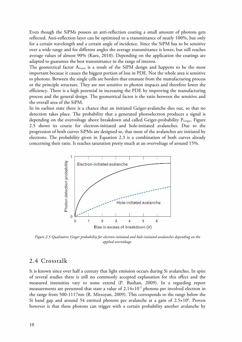
Even though the SiPMs possess an anti-reflection coating a small amount of photons gets reflected. Anti-reflection layer can be optimized to a transmittance of nearly 100%, but only for a certain wavelength and a certain angle of incidence. Since the SiPM has to be sensitive over a wide range and for different angles the average transmittance is lower, but still reaches average values of almost 90% (Kurz, 2010). Depending on the application the coatings are adapted to guarantee the best transmittance in the range of interest. The geometrical factor AGeom is a result of the SiPM design and happens to be the most important because it causes the biggest portion of loss in PDE. Not the whole area is sensitive to photons. Between the single cells are borders that emanate from the manufacturing process or the principle structure. They are not sensitive to photon impacts and therefore lower the efficiency. There is a high potential in increasing the PDE by improving the manufacturing process and the general design. The geometrical factor is the ratio between the sensitive and the overall area of the SiPM. In its earliest state there is a chance that an initiated Geiger-avalanche dies out, so that no detection takes place. The probability that a generated photoelectron produces a signal is depending on the overvoltage above breakdown and called Geiger-probability PGeiger. Figure 2.5 shows its course for electron-initiated and hole-initiated avalanches. Due to the progression of both curves SiPMs are designed so, that most of the avalanches are initiated by electrons. The probability given in Equation 2.3 is a combination of both curves already concerning their ratio. It reaches saturation pretty much at an overvoltage of around 15%.
Figure 2.5 Qualitative Geiger probability for electron-initiated and hole-initiated avalanches depending on the applied overvoltage.
2 .4 Crosstalk It is known since over half a century that light emission occurs during Si avalanches. In spite of several studies there is still no commonly accepted explanation for this effect and the measured intensities vary to some extend (P. Buzhan, 2009). In a regarding report measurements are presented that state a value of 2.14×10⁻⁵ photons per involved electron in the range from 500-1117nm (R. Mirzoyan, 2009). This corresponds to the range below the Si band gap and around 54 emitted photons per avalanche at a gain of 2.5×10⁶. Proven however is that these photons can trigger with a certain probability another avalanche by

11
ionizing an atom in the depletion layer of a neighboring cell. This process is referred to as crosstalk. The delay is in most cases due to the high speed of light and the short distances between the cells very short so that a crosstalk signal is not distinguishable from a real detection event. It just piles up to the unload charge of the SiPM. In Figure 2.6 the different scenarios for crosstalk are illustrated.
Figure 2.6 Illustration of the different crosstalk scenarios. Most of the recombination light leaves the detector through the surface or generates photoelectrons in a non-depleted region where they most often do not cause any effect on the detection (4, 5). But a small amount of the photons causes crosstalk either directly by travelling without indirection to a neighboring cell (1) or indirect when the photon is reflected from the backside of the detector and subsequently produces an electron-hole pair in another cell (2). It also can happen that a photoelectron or hole drifts from the non-depleted layer into the sensitive region (3). These crosstalk events are delayed and not distinguishable from afterpulsing (see chapter 2.5). Crosstalk is depending on the gain and therefore rises with the overvoltage. It was for a long time an unknown effect and the manufacturers wrongly rated the PDEs (see chapter 2.3) of their detectors too high. To reduce crosstalk significantly some of them now implement opaque trenches between the cells and a second high field region beneath the depletion layer to detain charge carriers drifting from the non-depleted substrate back into the detection zone. With these provisions it is possible to reduce the crosstalk by 1-2 orders of magnitude.
2.5 Afterpulsing Due to lattice imperfections in the material it is possible that during an avalanche process electrons get trapped. They will be released later on by tunnelling through the potential barrier and cause another delayed avalanche without photon interaction called afterpulse (AP). Most of the time APs trigger during the recovery time when the quenching process is still ongoing, so their charge is less then that of an actual photon initiated event. In this case

12
the APs can be identified in single photon spectrums. Sometimes however it happens that the electron is trapped longer and triggers an event after the quenching cycle what makes it indistinguishable to a photon event. Both kinds increase like crosstalk the PDE of SiPMs artificially and are therefore unwanted.
2.6 Thermal Noise The photon detection and therefore the signal creation in SiPMs takes place in the intrinsic layer, which is only faintly doped (see chapter 2.1), so that the overall conductivity here equals about the intrinsic conductivity of silicon. It is very low at standard conditions but according to the Fermi-Dirac distribution, which describes the partitioning of fermions into quantum states, not zero. Depending on the temperature, more or less electrons possess enough energy to tunnel through the gap between valence- and conduction band (1.12eV for Silicon at operation temperature) and separate from their nucleus. The statistical quantity of electrons in the conduction band at any time is given as
𝑛 = 𝑁! ∙ 𝑒! !!!!!!!! = 𝑁! ∙ 𝑒
! !!!!! 𝑛 =1𝑐𝑚!
Equation 2.4 𝑬𝑭: Fermi energy 𝚫𝑬: energy gap (1.12eV for Silicon at 300K) 𝑵𝑪: density of states in the conduction band 𝒌𝑩: Boltzmann constant
As soon as an electron enters the conduction band it is accelerated by the high voltage and triggers an avalanche, which is not distinguishable from a photon-initiated event. It occurs as dark rate in the signal and is proportional to the sensitive area. Hence, the larger the SiPM is, the bigger the thermal noise it produces. From chapter 2.3 one can also conclude, that with the Geiger-probability and therefore with the overvoltage also the dark rate rises. The only but very effective possibility to lower thermal noise is cooling. A temperature reduction of 8°C approximately halves the dark rate.
2.7 Perkin-Elmer Housing To test and operate SiPMs under the proposed working conditions the company Perkin Elmer developed housings (Figure 2.1), which are evacuated and come with built-in Peltier element (see chapter 4.1.2) and thermistor to regulate the temperature. The Peltier element’s hot side is connected to the brass housing to release the heat. It is therefore very important to cool the housing and keep its temperature steady to achieve the cooling capacity claimed by the manufacturer ( Table 2.1). Twelve pins connect TEC, thermistor and the SiPM board (wire bonds to signal and bias voltage) to the carrier board described in chapter 4.5.
Table 2.1 TEC specifications for the evacuated housings.
Hot Side Temperature 27°C 50°C ΔTmax (°C-dry N2) 64 72 Qmax (watts) 2.2 2.5 Imax (amps) 1.8 1.8 Vmax (vdc) 1.9 2.2 AC Resistance (ohms) 0.92 --

13
3 Development and construction of a dark box to characterize single photon counter
Ground-based γ-ray telescopes use ultra sensitive cameras to collect the faint Cherenkov light flashes mentioned in section 1. These cameras consist of several thousand ultra low light level detectors, which have to be tested and calibrated one by one prior to their installation to guarantee proper functionality. The key parameters of interest require measurements at the performance limit of the detectors and therefore need to be conducted in an adequate testing environment with optimal conditions. Total darkness and as little electromagnetic pickup as possible are the main criteria for these tests. According to the big number of devices to test a further demand is easy handling. The idea was to build a device that can contain various testing setups while granting generous access to every element in the installation. The testing procedure is usually for a big number of devices the same, so that once the setup is built, several calibrations and tests are conducted in the same environment and in between only the detector has to be exchanged. Therefore, right after closing the box, it should be ready to operate and provide perfect darkness without any additional shading, so that a new test can be launched without delay. Furthermore, shielding against electromagnetic pickup from outside should be given to avoid induced electric currents that might sophisticate the measurements.
3.1 Design & Features To fulfill the demanded requirements a wooden box has been designed and constructed as illustrated in Figure 3.1 below, with a lid that is compound of top and front panel. Due to this design it is easy to open and grants sufficient access to the whole interior.
Figure 3.1 - 3D blueprint of the Dark Box concept.

14
Figure 3.2 - 3D Sketch of the Dark Box in the closed state with rough dimensions. The 60° dip is necessary due to the U-profile described in the features.
Figure 3.3 – 3D Sketch of the Dark Box interior. Febrotec gas springs are intended to open the lid automatically. The inside was coated with an Aaronia+ EM-protection fleece and painted black to avoid undesirable reflections from
light sources within the box.

15
The basic wooden framework of the Dark Box was supplementary enhanced with aluminium angles to strengthen the kink in the lid and the following features:
U-profile & light barriers: To make the box lightproof a U-profile with metal tongue at the lid and groove integrated in the box walls covers the sides. The technique could not be applied to the front and the back because of the 90° opening angle of the lid. Therefore light barriers have been installed, which in principle represent half a U-profile (Figure 3.4). Soft rubber tape on the light barrier surface squeezes between the barrier and the wall of the box when it is closed. The two mechanisms prevent stray light from entering the box, even if it is exposed to bright daylight.
Figure 3.4 Sketch of the U-profile at the sides and the light barrier at the backside of the lid.
Febrotec gas springs: Similar to a trunk deck gas springs were implemented in the box design to lift the lid easy and smooth. The company Febrotec offers a wide variety of affordable commercial products right for this cause. Raw estimations yielded that two springs with a total initial force of 300N should be strong enough to lift the lid under a short lever, so that they do not occupy too much space within the box when it is closed. Figure 3.5 below shows the chosen model 0GS-N08KAT0150 with an extended length of 369mm and a stroke of 160mm. They were attached with the slated metal retainers from Febrotec at the box backside and the lid strengtheners (see Figure 3.1).
Figure 3.5 Gas spring 0GS-N08KAT0150 from Febrotec with 150N initial force.
Thorlabs breadboard: To build up measuring setups precisely in the box the aluminum breadboard MB3090/M from Thorlabs was installed. It has a size of 300x900mm and a metric M6 thread raster to mount optical equipment. It was fixed on an extendable plate connected with telescopic slides to the sides of the box (see Figure 3.1). With this arrangement the whole setup can be pulled out of the box for modifications.
Removable side panels: From time to time different plug-in bushings will be needed to wire all devices inside the box. Removable side panels hold them and make it easy to install additional ones later on. Soft rubber tape between the box walls and the side panel overlap impedes light from outside treading in. The feature also has a very useful ancillary effect. Instead of a side panel a whole box, or even several, can be connected in a row to expand the dark space for large setups.

16
Aaronia X-Dream+ fleece: The inside of the box was entirely coated with a copper fleece to screen the measuring setup against electromagnetic pickup (described in detail below).
3.2 Electromagnetic Shielding Electromagnetic pickup is a problem for all sensitive measurements. Static or alternating electromagnetic (EM) fields affect signals by producing threshold additional to thermal noise, which is always present. In times of wireless communication a wide range of bandwidths is used for broadcasting and data exchange. To avoid disturbance on the signal to measure, a protection mechanism that reduces, or even cuts out this error source would be advantageous. A reduction of EM pickup directly results in a higher sensitivity for the measurement. The conventional method for EM shielding is a Faraday cage, which consists of a metallic layer around the protected area. The shielding is best if the electrons can move with the least possible resistance through the whole cage. Static electric fields influence electrons and move them along the EM field from one side of the cage to the other. Due to the movement of charge carriers a second electrostatic field emerges that is oriented opposite to the interfering field and has the same strength. A field-free zone within the Faraday cage is the consequence. Perfect Faraday cages offer in principle infinite protection against static electric fields and can be realized quite well in practice. Is the wavelength of an alternating electric field large compared to the size of a perfectly conducting cage, the influence mechanism still provides protection. It is not ideal anymore though and depends on the conductivity of the material. Against magnetic fields only ferromagnetic materials provide protection by adjusting their molecular magnets. This effect is comparable to electrostatic influence and not further discussed here because static interfering magnetic fields are rare and not supposed to occur close to the setup. Electromagnetic radiation that has a wavelength comparable to the size of the cage or smaller is diminished by the following mechanism: the induction of eddy currents on the surface of the cage and a resulting field according to Lenz’s law act contrary to the incoming one and decrease it therefore. This effect is dependent on the material’s characteristic attenuation coefficient for the given wavelength and its thickness. The Beer-Lambert law describes the damping of electromagnetic radiation in materials.
𝐼 𝑥 = 𝐼! ∙ 𝑒!! ! Equation 3.1
𝝁: attenuation coefficient 𝒙: penetration depth The equation is valid for solid materials. Holes in the layer or non-conducting connections on borders lower the damping, especially when they reach a size comparable to the wavelength of the radiation. Copper has a very high attenuation coefficient and is therefore mainly used for EM shielding. A solid layer for the whole box however would be very heavy and difficult to install for it has to have a perfect galvanic connection on every edge to provide good shielding. Hence, a commercial solution has been selected for the measuring box. The company Aaronia AG offers a fleece made of copper slivers that pledges a damping of more than 80dB, up to a frequency of 10GHz. The best performance is given with the version X-Dream+ that is additionally self-adhesive and therefore easy to install on the inside of the wooden box. It is necessary that in the closed state all the edges of the box get in conducting contact so that the shielding is optimal.

17
4 Upgrade for performance measurements of Sil icon Photomultipliers
To perform all the intended measurements on SiPMs additional equipment is required and has to be installed in the box.
Figure 4.1 Image of the complete setup (taken by Florian Frank). The LED pulser (4.6) is installed on a z-y-table. It can be moved between two rails along the x-axis to adjust its position in all three dimensions.
In between the light pulser and the cooling mount is a construction that holds a neutral density filter (4.7), which reduces the light intensity on the SiPM and also is adjustable in z-direction. The SiPM is installed together with a
PIN diode (4.2) in the cooling mount (4.1) and connected with a carrier board (4.5) to an amplifier (4.4).
4.1 Cooling Mount The SiPMs to test are embedded in a vacuum housing (see chapter 2.7), which already includes a Thermoelectric Cooler (TEC, see chapter 4.1.2). These elements provide a heat stream and therefore cool a source by heating up another one. For a constant cooling performance the hot side needs to release the fed heat to the surroundings and keep a steady temperature. If it comes to heat accumulation at this end, the whole device warms up and the cooling performance deteriorates. To prevent this effect the mount that holds the SiPM and the PIN diode has therefore been designed accordingly. It is made entirely of copper to provide a good heat flow and has a ventilator with cooling rips to support the heat transport to the surrounding air. The ventilator comes from Titan, runs under 12V DC and is actually intended to cool CPUs (Figure 4.2). To guarantee a good thermal connection between SiPM and mount the clearance matches exactly the dimensions of the brass housing (see chapter 2.7). During the experiment it will be necessary to verify that the light intensity on both detectors is the same. Therefore the

18
distance between the detectors has been held small and the mount was equipped with a rotation mechanism to switch the position of PIN diode and SiPM.
Figure 4.2 Wraparound view of the cooling mount with installed SiPM and PIN diode.
4.1.1 Peltier Effect
In 1821 Thomas Johann Seebeck discovered the Thermoelectric Effect (Seebeck Effect). It occurs when the junctions of two semi conductors with different conduction band energy levels in a circuit possess different temperatures. The result is a voltage as pictured in Figure 4.3 on the left, which depends on the temperature difference and the two materials.
𝑈 = ( 𝑆! 𝑇 − 𝑆! 𝑇 ) 𝑑𝑇!!
!!
Equation 4.1 𝑺𝑨, 𝑺𝑩 are material constants The inverse to the Seebeck effect was discovered 13 years later by Jean Peltier and is named after him. It is described as follows: when a current is applied to the setup devised by Seebeck a heat flow occurs between the two junctions. It is proportional to the applied current and warms up one side while cooling the other (Figure 4.3, right).
Figure 4.3 The left image illustrates the Seebeck effect and the right image the Peltier effect. Both are depicted for T2 >T1 and EC (A) > EC (B).

19
The effect is caused by the difference between the energy levels of the semi conducting materials. To cross the border from the material with the lower conduction band energy level (EC) to the other one the electrons enter a higher energy state and therefore lose, according to law of energy conservation, kinetic energy. The summed up loss over all electrons crossing the barrier equals a decrease of inner energy in the material and therefore its temperature; the interface cools down. At the other connection point the electrons jump from the high conduction band energy level to the lower one and gain kinetic energy, the interface heats up. The heat stream (Equation 4.2) is directly proportional to the applied current and depends on the materials.
𝑄 = Π!" ⋅ 𝐼 = Π! − Π! ⋅ 𝐼 Equation 4.2
𝚷𝑨 and 𝚷𝑩 are the so-called Peltier constants. They are conditional on material and temperature.
4.1.2 Thermoelectric Cooling
According to Peltier’s principle it is possible to create devices that generate a constant heat flux against the temperature gradient with the use of electrical power. These Peltier elements or Thermoelectric Coolers (TEC) have bad efficiencies of typically 5 - 10% of the ideal Carnot-cycle but a very fast response. The additive ability to heat and cool makes them a suitable solution for controlling cycles to regulate the temperature precisely. The possible heat flux however and therefore the cooling performance is not infinite. The ohmic resistance in the device causes losses in form of heat, so that high currents warm up the whole device and overweigh at a certain point the cooling effect. With the hot side at room temperature Peltier elements reach maximum temperature gradients of 60 to 70°C. To keep the temperature in the setup steady the temperature controller TED4015 from Thorlabs was used. It features a PID regulation circle that measures continuously the temperature of the SiPM by reading the resistance at the thermistor and adjusting the TEC current accordingly (Figure 4.4).
Figure 4.4 Schematic of the PID regulation cycle in the system. The SiPM mount is made of copper to support the
heat transport from the housing to the ventilator and finally to the surrounding air. Due to the current limit of the Peltier element in the Perkin Elmer housing the lowest achievable temperature that can be kept steady in the cycle is far above the indicated one. With thermal grease it can be adjusted to maximal -15°C.

20
4.2 PIN Diode (Posit ive Intrinsic Negative Diode) The only difference between a common PN diode and a PIN diode is an intrinsic layer between the doped zones. It is not or only faintly doped and high resistant because of the low intrinsic conductivity of semiconductors (see chapter 2.6). Figure 4.5 below shows the typical architecture of PIN diodes and their doping profile as well as the spatial concentrations of electrons and holes.
Figure 4.5 Sketch of the PIN diode working principle. Depending on the applied bias voltage two different operation modes for PIN diodes are possible. An applied reverse voltage results in a depletion layer that is far bigger than in convenient PN diodes. As a result one can achieve very high blocking voltages. However, the most common operation mode is a forward applied bias voltage that forces charge carrier to drift into the intrinsic layer and therefore lowers its resistance. The emerging electric field increases the drift speed of electrons and holes through the depletion zone and therefore enhances the high frequency response capability. Above 10 MHz the charge carrier do not have enough time anymore to leave the intrinsic layer between two signals so that the diode does not behave like a rectifier anymore, but rather like an AC resistor. Its value is adjustable by the applied bias voltage. For the process is linear over a wide range this components are used as DC controlled resistors, HF-switches or find utility in many other high frequency circuits. A further application of PIN diodes is the use as photo diode, where the forward bias mode allows fast signal processing e.g. for optical data transmission. In the measuring setup a Hamamatsu S1337BQ PIN diode (10x10mm) was installed in the cooling mount right next to the SiPM to measure the average light intensity emitted by the LED pulser (see chapter 4.6). It does not need to be biased and is just connected directly to a Keithley 485 autoranging picoammeter. It serves as reference to calculate the SiPM’s PDE (see chapter 5.3) and therefore has to be calibrated prior to its use.

21
4.3 Calibration with Quantum Efficiency Measuring Device A prior working student at the MPP already developed a device to calibrate PIN diodes by comparing them to a reference detector with exactly known spectral quantum efficiency. A Deuterium & Tungsten-Halogen Hybrid Based light source (ASTN-D1-W150) produces light in the whole spectrum from 180 to 2600nm. Before it enters a dark box the light goes through a monochromator, which uses two gratings to split the spectral components of the light beam geometrically. With this technique it is possible to select a spectral range with a precision of only 0.2nm and an accuracy of ±0.6nm. Behind the monochromator a filter wheel eliminates the double wavelengths generated by the gratings. A lens in the box panel is focusing the light on the PIN diode to measure. The monochromator and the filter wheel are controlled over a RS232 port by a LabView program, which automatically adjusts the light source to certain wavelengths and scans a free selectable spectrum. The user can choose the range to measure and the step size to increase or decrease the resolution of the spectral analysis.
Figure 4.6 Sketch of the QEMD.
The PIN diode is connected to a Keithley 6485 picoammeter that transmits the measured photo current over a GPIB port to the computer. The value can be accessed by the software and is written together with the corresponding wavelength into a text file. For the calibration of the used PIN diode the settings were set to a range from 200 – 1000nm and a step size of 10nm. A PIN diode calibration takes place as follows: First the reference diode has to be measured. The pedestal current without light source is taken before and after the measurement to subtract the average background from the outcome later. After that the light source is adjusted automatically to each wavelength in the selected range to perform a measurement of the photocurrent and store it in the file. Now the same steps have to be repeated for the sensor, which has to be calibrated. With the given quantum efficiency (QE) curve of the reference diode and the two measurement series the QE of the un-calibrated diode can be calculated.
𝑄𝐸!"#"$"%&"𝐼!"#"$"%&"
= 𝑄𝐸!"#𝐼!"#
→ 𝑄𝐸!"# = 𝑄𝐸!"#"$"%&"𝐼!"#"$"%&"
∙ 𝐼!"#
Equation 4.3
In the Hamamatsu datasheet for the calibration diode the efficiency is given in units of A/W (see Figure 4.7), photo current per incoming radiant power. To get the QE in percentage one has to do a conversion (selected points have been converted and are given in Figure 4.8).
𝑄𝐸 = 𝐴𝑊 ∙ ℎ ∙ 𝑐!𝑒 ∙ 𝜆
Equation 4.4 𝒉: Planck constant 𝐜𝟎: vacuum speed of light 𝐞: elementary charge 𝜆: wavelength

22
Figure 4.7 Spectral sensitivity of the used PIN diode S1337-BQ, indicated by Hamamatsu.
In figure Figure 4.8 below the result of the measurement is given (red dots) together with the specifications for the diode (green dots) and the characteristics of the reference diode (blue dots). According to the manufacturer indications the used PIN diode should have a sensitivity similar to the reference diode, but the actual curve shows deviation, especially in the range below 400nm. This is because the PIN diode was bought un-calibrated. It is common that the manufacturer gives a typical curve that can vary from device to device. Furthermore, environmental influences on the diode can change its characteristics over time and lower its QE.
Figure 4.8 Calibration of the PIN diode. The blue line shows the QE of the reference diode, the red line corresponds to the measured diode from Hamamatsu and the green markers represent the indications in the Hamamatsu datasheet.
wavelength [nm]200 300 400 500 600 700 800
Qua
ntum
Effi
cien
cy [%
]
30
40
50
60
70
80
Calibration of the Hamamatsu PIN diode

23
4.4 Amplifier To amplify the weak SiPM signal in the range of around 10-100pA the HSA-Y-2-40 from Femto was plugged between the diode and the oscilloscope (LeCroy WavePro 7300A). The short pulses of less than 10ns require high-speed amplification with a minimum bandwidth of at least 1GHz to get a satisfying result. The Femto amplifier can fulfill this requirement easily with a bandwidth of 1.9 GHz and a rise time of only 185ps. It provides a gain of 40dB what equals a multiplication factor of 100. To keep the EM pickup (see chapter 3.2) as low as possible the leads between SiPM and amplifier should be held very short. After the amplification the noise does not have much impact anymore because the signal-to-noise ratio is now almost a hundred times bigger.
Figure 4.9 Schematic of the Femto HAS-Y-2-40.
4.5 Readout Board To connect the ports of the SiPM to the temperature controller, the bias voltage and the amplifier a carrier board has been designed (Figure 4.11). It can be easily plugged to the 12 pins of the SiPM case and permits therefore a quick exchange of the detector. The sample was additionally soldered on a plate as shown in Figure 4.10. As mentioned in the previous section the link between SiPM and amplifier should be as short as possible to avoid pickup. Therefore, the carrier board was constructed to be mountable directly to the amplifier without lead. This principle has also the advantage of more stability in comparison to a flying board and takes less effort than constructing a separate mount.
Figure 4.10 SiPM mounted on the Carrier Board.
Figure 4.11 Image of the Carrier Board (top view).

24
Additionally to the SMA amplifier connection (brass) the board offers three LEMO plugs for SiPM power supply, thermistor and TEC control current. The actual schematic is very simple and partly adapted from a Hamamatsu recommendation to connect SiPMs. On the anode side, parallel to the amplifier, a 47Ω resistor to ground converts the photocurrent into a voltage, which can be amplified by the Femto. To avoid pickup admitted from the voltage supply a so-called Π-filter, consisting of two 22nF capacitors and a 10kΩ resistor, cuts out frequencies above around 1kHz (see simulation in the appendix 9.4) what includes all kinds of broadcasting and data transmission.
Figure 4.12 Schematic of the SiPM readout board Figure 4.13 Layout of the SiPM readout board
4 .6 LED Pulser To conduct the conceived PDE and breakdown voltage measurements an adequate light source is needed. Single wavelengths for a spectral analysis can be obtained in three different ways: Lasers, LEDs or broad-spectrum light sources in combination with monochromators and filter wheels (see QEMD in chapter 4.3). Lasers provide high frequencies, narrow pulses and high intensities but they are also very expensive. A detailed spectral analysis would lead to enormous costs of the necessary equipment. Monochromator regulated light sources provide a wide spectral range but it is very difficult to gain narrow light pulses with a high frequency. Thus, LEDs seem to be a good solution due to their low cost, fast response and availability for a wide range of wavelengths. For the PDE measurement six low cost standard LEDs with wavelengths of 355, 375, 405, 450, 505 and 575nm have been selected to test the arrangement. To generate short narrow pulses in the nanosecond regime with LEDs is a known challenge, which occurred earlier at the Max Planck Institute for Physics, so a complying device already exists. Only a single modification had to be done. To guarantee a diffuse distribution of the LED light a diffusor plate was glued in front of the hole where the light is released. Its degree of diffusion was checked in the switching test (see chapter 5.3). Besides the diffusor the LED pulser contains two circuits. The first happens to be a trigger board that provides controls for intensity and frequency (maximum 1kHz) and an external trigger input. Power is supplied by two 9V batteries or optional by a 15V DC external source. The whole board provides a trigger signal for the second circuit, the so-called Kapustinsky pulser.

25
4.6.1 Kapustinsky Circuit
Already in 1985 J.S. Kapustinsky published a paper with his team, which describes a circuit to run a LED in ultra short pulse mode (J .S . Kapustinsky, 1985). The schematic consists of only eight components (most of them out-of-the-shelf products). Therefore it is very easy to fabricate and also cheap.
Figure 4.14 Original schematic of the Kapustinsky LED pulser.
At the input one has to apply a trigger pulse with a minimum length of 150ns riding on a DC bias voltage of 0-24V. These pulses come from the first board (see chapter 4.6), which provides also a bias level of 15V, limited by a fixed voltage regulator. The DC bias voltage charges the 100pF capacitor steadily over a 100kΩ resistor until the trigger pulse switches the transistors and it unloads over the LED to ground. Wired according to Kapustinsky’s principle the LED emits very short light pulses without derogating its lifetime.
4.6.2 Pulse shape and Intensity
To get an idea how the actual light emission of the used LEDs is correlated to the driver signal and the trigger frequency a measurement was set up. It is only quantitative to give a rough estimation about the LED pulse shape and the maximum average light intensity depending on the trigger frequency. For the PDE measurement it is important that on one hand the SiPM is flashed by narrow pulses with an intensity beyond saturation level and on the other hand that the not so sensitive PIN diode receives a high average intensity to measure with good accuracy. The important factor here is frequency. Due to the principle of the Kapustinsky pulser it is not possible to generate pulses with arbitrary high frequency. It is limited by the charge time of the 100pF capacitor.
𝑓!"! =15𝜏 =
15 𝑅𝐶 =
15 ∙ 100𝑘Ω ∙ 100𝑝𝐹 = 20𝑘𝐻𝑧
Equation 4.5 In case one exceeds the frequency limit, the light pulses lose intensity or stop occurring periodically. This happens when the time between the pulses is too short to load the capacitor to the level, which is necessary to flash the LED. For the measurement the LED pulser was set up with the 375nm LED and put in the dark box illuminating a PMT behind a neutral density filter, which shifted the intensity beyond

26
the saturation level of the detector. With a varying trigger frequency the pulse width and the quantitative light intensity were examined as given in Table 4.1 below.
f
[kHz] FWHM
[ns] Amp [mV]
I (PMT) [nA]
1 4.4 766 126 2 4.3 763 249 5 4.4 764 625
10 4.3 761 1231 20 4.3 658 2120 25 4.2 593 2332 30 4.1 523 2421 35 4.0 477 2526 40 4.0 424 2527 45 4.0 366 2454 50 3.9 302 2188
Table 4.1 Pulse shape and intensity measurements on the LED in dependency of the pulse frequency.
The photo current I(PMT) represents only the progression of the light intensity and not its actual value. The test prove the assumption that the light emission produced by the LED pulser is directly proportional to the trigger frequency, up to around 20kHz (Figure 4.15). At this point the curve flattens but the intensity still increases until it reaches its maximum at around 35kHz. After the peak it drops slowly to the cutout frequency of roughly 52kHz where the light emission stops completely.
Figure 4.15 PMT photocurrent depending on the trigger pulse frequency. The devolution is similar to the actual light emission of the LED pulser
The pulse width also appears to be about even up to 20kHz where it starts do descend slowly (Figure 4.16). From the measurements one can conclude that the optimal trigger frequency for the proposed PDE measurement (see chapter 5.3) is around 35kHz. Here the light output has a maximum and a pulse width of 4.0ns.
pulse frequency [kHz]0 10 20 30 40 50
phot
o cu
rrent
PM
T [n
A]
0
500
1000
1500
2000
2500
Light Emission LED in dependency of trigger frequency

27
Figure 4.16 Pulse width depending on the trigger frequency.
4.7 Neutral Density Filter For the PDE measurement (see chapter 5.3) the signal of the SiPM has to be compared directly to the reference PIN diode. The challenge here is that below the saturation limit of the SiPM the average light level is due to the maximum pulse frequency of 35kHz too low for the PIN diode to produce a measurable photocurrent. Therefore the light intensity was increased and subsequently dimmed with a neutral density filter, installed right in front of the SiPM (see Figure 4.1). With the exactly known absorption behaviour of the filter the light intensity on the SiPM can be calculated by multiplying the intensity on the reference diode with the transmission factor of the filter for the given wavelength. A complete filter characterization can be found in the appendix 9.3.
Figure 4.17 Transmission curve of the used 50% transmission filter (measured by Hanna Kellermann).
pulse frequency [kHz]0 10 20 30 40 50
puls
e w
idth
[ns]
2
2.5
3
3.5
4
4.5
5
pulse width LED in dependency of trigger frequency

28
5 Measurements & Characterization of SiPMs Within this section two SiPM prototypes from MEPhI with an active area of 1x1mm (Figure 2.1, left image) were analysed. The sample devices derive from the series 100A and 100B, which both have a cell size of 100µm, so that their total number of cells sums up to 100. They are embedded in Perkin Elmer housings (see chapter 2.7) to regulate the temperature to around -10°C and keep it steady. The main difference between the two samples is the implementation of optical trenches between the single cells in the 100B detector. They are intended to reduce the optical crosstalk significantly by detaining generated photons from reaching other cells (see chapter 2.4). The 100B sample however showed a very bad charge resolution (see Figure 5.1) so that only the breakdown voltage could be determined more or less properly. The crosstalk values were not precisely measurable, fluctuated heavily depending on the chosen trigger level and exceeded any rational numbers, so that the crosstalk and PDE measurements were cancelled. For the 100A device in contrary a complete characterization, except afterpulsing, was conducted and the results compared to similar measurements.
5.1 Determination of Gain and Breakdown Voltage By definition the SiPM gain is the ratio between the generated charge of a single photon detection event within a quenching cycle and the elementary charge (Kurz, 2010).
𝐺!"#$ = 𝑄!!!!𝑒 =
1𝑒 ∙ 𝐼
!!!! 𝑑𝑡
Equation 5.1
The charge a single photon count produces can be measured directly or calculated by subtracting the charge of an n-photon signal from a (n+1)-photon signal. To compensate the influence of the Femto amplifier the result has to be divided additionally by its amplification factor.
𝐺!"#$ = 𝑄!!! !!! − 𝑄! !!!
𝑒 ∙ 𝐺!"#
Equation 5.2
The measurement was set up the following way: a frequency generator (SRS DS345) triggered the LED pulser and also the oscilloscope (sync channel) with a frequency of 35kHz. To achieve a low light level of only a few photons per pulse at the detector the LED pulser (equipped with the 375nm LED) was positioned in around 35cm distance from the SiPM and adjusted to a low intensity (see chapter 4.6). During the whole measurement the TED4015 (see chapter 4.1.2) regulated the temperature of the SiPM and assured it to be -10.18°C ± 0.05°C for the 100B and -8.50°C ± 0.15°C for the 100A measurement. The whole setup is illustrated in Figure 4.1. With the built-in oscilloscope function histograms were produced for different bias voltages by integrating the SiPM signal over time with an integration window of 10ns for 100B, 20ns for 100A and at least 10,000 events (Sweeps). To determine the gain precisely a Root program has been written (see appendix 9.1.1), which divides the results by the oscilloscope impedance (50Ω) to get the actual charge and fits a multi-gauss curve according to Equation 5.3 on the corrected histograms. All fits can be found in the appendix 9.2.1 and 9.2.2.

29
𝑁 𝑥 = 𝐴! exp − 𝑥 − 𝜇! !
2 𝜎!!
!
!!!
Equation 5.3 𝑨𝒊: maximum peak counts 𝝁𝒊: charge of the peak 𝝈𝒊: standard deviation of the gauss curve
With the multi-gauss fit the exact position of each peak can be determined, what is required to calculate the gain. After admitting how many peaks the fit should contain in the program’s configuration, it appoints automatically the corresponding fitting function at runtime. For every fit however, suitable starting parameters have to be supplied manually, so that it diverges against the real distribution. Only with this fitting procedure it was at all possible to determine gain and breakdown voltage for the 100B device. As one can see in Figure 5.1 and Figure 5.2 below the peaks overlap heavily and shift each other in x-direction what causes simple gauss fits to mislead and provide wrong charge values.
Figure 5.1 Screenshot of the oscilloscope display during a gain measurement of the 100B detector. The persist display (top) was set to permanent.
Figure 5.2 Plot for the 100B detector. Created by the Root evaluation program with corresponding multi-gauss fit.
Charge Q [pC]0 5 10 15 20 25 30 35 40
-1210×
Cou
nts
0
50
100
150
200
250
300
350
400
C)°Gain 35.478V (-10.18

30
Due to the perfect charge resolution of the 100A device (Figure 5.3) the evaluation of its histograms could have been conducted with simple gauss fits just as good as with multiple ones. The program was already written though and served therefore also for this analysis.
Figure 5.3 Screenshot of the oscilloscope display during a gain measurement of the 100A detector. The persist display (top) was set to 0.5s duration.
Figure 5.4 Plot for the 100A detector. Created by the Root evaluation program with corresponding multi-gauss fit.
To determine the gain the program calculates from the fit parameters the charge difference between the peaks. For a better accuracy the difference between pedestal and 1phe peak and 1phe and 2phe peak are calculated and averaged. The results for the 100B detector are given in Table 5.1. With the evaluation results from 5.1 the breakdown voltage could be estimated by extrapolating the devolution of the gain to zero. In a properly working device the gain rises, up to an overvoltage of at least 5%, directly proportional with the bias voltage, so that a linear fit can be applied (see Figure 5.5). At higher values the limited availability of charge carriers takes effect and the curve flattens down.
Charge Q [pC]-2 0 2 4 6 8 10
-1210×
Cou
nts
0
100
200
300
400
500
600
C)°Gain 35.69V ( T = -8.58

31
Vbias
[V] Qpedestal
[pC] Q1phe
[pC] Q2phe
[pC] SiPM gain
33.787 -0.014 2.171 -- 136392 33.890 0.015 2.618 5.013 155993 34.015 0.002 3.112 6.288 196192 34.080 -0.005 3.164 6.353 198439 34.203 -0.080 3.900 7.981 251592 34.293 -0.059 4.358 8.906 279806 34.402 -0.005 5.382 10.67 333177 34.526 -0.045 5.408 10.86 340356 35.091 -0.090 6.973 14.22 446629 35.478 -0.110 7.678 15.93 500624 36.030 -0.021 9.969 19.44 607397
Table 5.1 Evaluation results of the 100B single photon spectrums to determine the gain.
Figure 5.5 Gain of the 100B detector in dependence of bias voltage with breakdown extrapolation.
With the aid of the fitting parameters p0 and p1 the breakdown voltage could be estimated by calculating the intersection of the linear fit with the x-axis (bias voltage).
𝐺𝑎𝑖𝑛 = 3.013 ∙ 10! !! ∙ 𝑉!"#$ − 1.005 ∙ 10! ∶= 0
Equation 5.4
→ 𝑉!"#$%&'()(100𝐵 @− 10.18°𝐶) = 1.005 ∙ 10!
3.013 ∙ 10!𝑉!! = 33.4𝑉 Equation 5.5
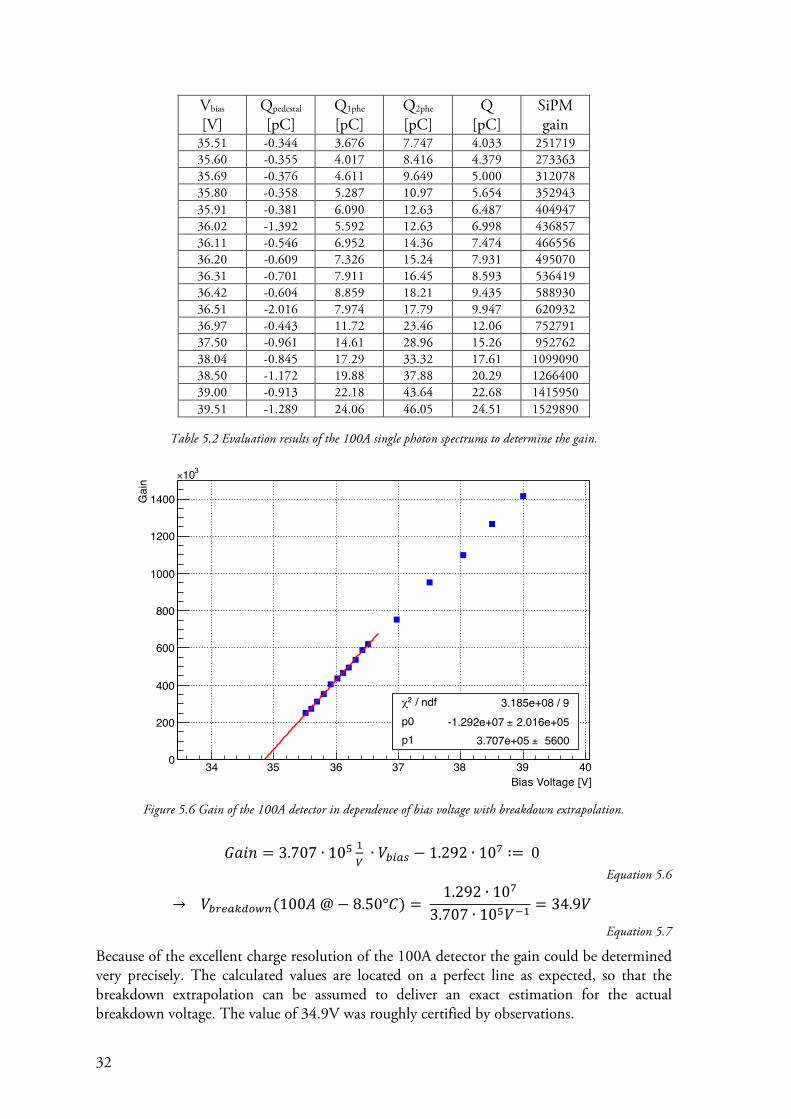
Due to the bad charge resolution of the 100B detector the determined gain values fluctuate around the proposed linear line. The breakdown value of 33.4V however could be roughly certified by observations. The just described methods were also deployed to determine gain and breakdown voltage for the 100A detector. The results are presented in Table 5.2 and Figure 5.6.
Bias Voltage [V]33 33.5 34 34.5 35 35.5 36
Gai
n
0
100
200
300
400
500
600
310×
/ ndf 2r 8.988e+08 / 6p0 6.226e+05± -1.005e+07 p1 1.823e+04± 3.013e+05
/ ndf 2r 8.988e+08 / 6p0 6.226e+05± -1.005e+07 p1 1.823e+04± 3.013e+05
32
Vbias
[V] Qpedestal
[pC] Q1phe
[pC] Q2phe
[pC] Q
[pC] SiPM gain
35.51 -0.344 3.676 7.747 4.033 251719 35.60 -0.355 4.017 8.416 4.379 273363 35.69 -0.376 4.611 9.649 5.000 312078 35.80 -0.358 5.287 10.97 5.654 352943 35.91 -0.381 6.090 12.63 6.487 404947 36.02 -1.392 5.592 12.63 6.998 436857 36.11 -0.546 6.952 14.36 7.474 466556 36.20 -0.609 7.326 15.24 7.931 495070 36.31 -0.701 7.911 16.45 8.593 536419 36.42 -0.604 8.859 18.21 9.435 588930 36.51 -2.016 7.974 17.79 9.947 620932 36.97 -0.443 11.72 23.46 12.06 752791 37.50 -0.961 14.61 28.96 15.26 952762 38.04 -0.845 17.29 33.32 17.61 1099090 38.50 -1.172 19.88 37.88 20.29 1266400 39.00 -0.913 22.18 43.64 22.68 1415950 39.51 -1.289 24.06 46.05 24.51 1529890
Table 5.2 Evaluation results of the 100A single photon spectrums to determine the gain.
Figure 5.6 Gain of the 100A detector in dependence of bias voltage with breakdown extrapolation.
𝐺𝑎𝑖𝑛 = 3.707 ∙ 10! !! ∙ 𝑉!"#$ − 1.292 ∙ 10! ∶= 0
Equation 5.6
→ 𝑉!"#$%&'()(100𝐴 @− 8.50°𝐶) = 1.292 ∙ 10!
3.707 ∙ 10!𝑉!! = 34.9𝑉 Equation 5.7
Because of the excellent charge resolution of the 100A detector the gain could be determined very precisely. The calculated values are located on a perfect line as expected, so that the breakdown extrapolation can be assumed to deliver an exact estimation for the actual breakdown voltage. The value of 34.9V was roughly certified by observations.
Bias Voltage [V]34 35 36 37 38 39 40
Gai
n
0
200
400
600
800
1000
1200
1400
310×
/ ndf 2r 3.185e+08 / 9p0 2.016e+05± -1.292e+07 p1 5600± 3.707e+05
/ ndf 2r 3.185e+08 / 9p0 2.016e+05± -1.292e+07 p1 5600± 3.707e+05

33
5.2 Determination of Crosstalk The measurement of optical crosstalk (see chapter 2.4) was conducted with a similar setup as described in the previous section. Besides the not used light source it stayed principally identical. To avoid reflections or any other deranging effects the field of few of the SiPM was completely cleared. Without any ambient light only thermal noise is assumed to produce avalanches. In a cooled detector state the probability that two events occur at the same time within the 5ns integration window is very small and therefore negligible (see dark rate, chapter 5.3.2). From these assumptions one can conclude that all signals with a multiple charge of the 1phe peak are a direct result of optical crosstalk. To prove total darkness the photocurrent was recorded with the PIN diode (see chapter 4.2) during the entire measurement. It fluctuated slightly around an average of 0.2pA, which corresponds to the dark noise of PIN diode plus lead to the picoammeter. Due to the bad charge resolution of the 100B detector (as already mentioned in 5) the crosstalk could not be measured properly, so in the following only the measurement for the 100A device is presented. To determine the crosstalk for different bias voltages, again histograms were recorded at a temperature of -8.62°C ± 0.20°C.
Figure 5.7 Screenshot of the oscilloscope display during a crosstalk measurement of the 100A detector. The persist display was adjusted to a duration of 0.5s so that the crosstalk events are clearly visible against the 1phe signal.
This time however the trigger was not set to an external source but to the signal itself. To ensure that the 1phe peak was within the adjusted trigger level the gain values from the previous chapter were used to assess the expectable 1phe charge and compare it to the measurement.
𝑄! !!! = 𝑒 ∙ 𝐺!"#$ 𝑉!"#$ ∙ 𝐺!"# Equation 5.8
Once the first peak in the histogram had been verified to correspond to 1phe signals, the crosstalk was determined with a method adopted from the article “Characterisation Studies of Silicon Photomultipliers” (Patrick Eckert, 2010), which was also applied in the diploma thesis “Precision Measurements of Ultra-fast Low Light Level Candidate Sensors for the CTA Project” by Matthias Kurz (Kurz, 2010). It is based on the assumption that all counts with a charge below 0.5Q1phe correspond to noise and all counts above 1.5Q1phe to crosstalk.

34
For the evaluation of the measurements the Root program mentioned before had been modified (see appendix 9.1.2). The number of peaks was set to one so that the program fitted a simple gauss curve to the histograms. Because of the trigger method this time there was no pedestal peak but the principles stayed the same (Figure 5.7). With the fit parameter that indicates the position of the 1phe peak the program computes the values 0.5Q1phe and 1.5Q1phe and sums up the 1phe counts of the range in between. Subsequently it integrates the crosstalk events with a charge of 1.5Q1phe to infinite. Finally the crosstalk rate is calculated according to the formula in Equation 5.9 and printed on screen.
𝑐𝑟𝑜𝑠𝑠𝑡𝑎𝑙𝑘 = 𝑐𝑜𝑢𝑛𝑡𝑠!.!!!!!!
!.!!!!!!
𝑐𝑜𝑢𝑛𝑡𝑠!!.!!!!!!
Equation 5.9
The computed values for different bias voltages are given in Table 5.3 and were illustrated in Figure 5.8 below. All histograms with the corresponding fit can be found in the appendix 9.2.3.
Vbias [V]
Crosstalk [%]
35.51 1.03 36.02 2.78 36.50 5.74 36.97 8.49 37.50 13.80 38.08 19.38 38.50 23.97 39.01 31.11 39.53 37.23 39.98 44.23
Table 5.3 Evaluation results of the crosstalk measurements for different bias voltages.
Figure 5.8 Devolution of Crosstalk for the 100A detector in dependence of the bias voltage.
Bias Voltage [V]36 37 38 39 40
Cros
stal
k [%
]
0
10
20
30
40
50
60

35
The determined crosstalk values of ~6% at an overvoltage of 5% and ~45% at an overvoltage of 15% are extremely high, but still rational. Due to the missing trenches in this device (see chapter 2.4) and the typical crosstalk devolution of the curve the results can be assumed to be valid.
5.3 Determination of PDE (Photon Detection Efficiency) To determine the PDE (see chapter 2.3) of the 100A detector a principle devised by Adam Nepumuk Otte in his PhD thesis (Otte, 2007) has been used. It describes how to measure the actual photon detection efficiency of SiPMs without the influence of crosstalk and is applied as follows: the basic idea is to illuminate the SiPM to measure and a light detector with known detection efficiency by a pulsed light source, so that both devices are exposed to the same light intensity. In this measurement the reference detector will be a calibrated PIN diode (see chapter 4.2 & 4.3) and the light source the LED pulser described in 4.6. With the measured photocurrent (IPIN) and the known quantum efficiency (QEPIN) of the PIN diode, as well as the average photon counts of the SiPM the PDE can be calculated.
𝑃𝐷𝐸 = 𝜇 ∙ 𝑒 ∙ 𝜈!" ∙𝑄𝐸!"#𝐼!"#
∙ 𝐴!"#𝐴!"#$
Equation 5.10 𝝁: average number of SiPM photon counts per trigger event 𝐞: elementary charge 𝝂𝑳𝑺: light source frequency 𝑨𝑷𝑰𝑵,𝑨𝑺𝒊𝑷𝑴: detection areas of the detectors
In the equation all parameters besides µ are either known (𝑒, 𝜈!", 𝐴!"# , 𝐴!"#$ , 𝑄𝐸!"# ) or directly measurable (𝐼!"# , see chapter 4.2). To get µ one could record a single photon spectrum as for the gain and crosstalk measurements, count the events for all the single peaks and calculate the average number of photons. This method however is difficult to execute and also afflicted with crosstalk. A. N. Otte therefore took advantage of the fact that the number of photons hitting the detector is Poisson distributed for low light intensities, so that µ can be calculated when the number of events is known, in which no photon hits the detector (pedestal).
5.3.1 Poisson Distribution
The Poisson distribution describes the probability of how many times a repeatedly performed Bernoulli experiment is successful in a certain interval of time and/or space. As such, one refers to, if the experiment has only two possible outcomes and the chance of success is small (Papula, 2006). The distribution is defined as
𝑁 𝑘 = 𝑃(𝑋 = 𝑘) = 𝜇!
𝑘! 𝑒!!
Equation 5.11 𝑿: random variable 𝒌: number of successful events within the time interval 𝝁: average number of successful events within the time interval
In the PDE measurement the detection of a single photon in the SiPM is seen as Bernoulli experiment and the integration window as time interval. The probability that no photon hits the detector is given in Equation 5.12 and logically not afflicted by crosstalk. It is in theory sufficient to calculate the average number of photons hitting the detector (Equation 5.13).

36
𝑃 0 = 𝑁 0𝑁!"!#$
= 𝑒!!
Equation 5.12
→ 𝜇 = −ln 𝑁(0)𝑁!"!#$
Equation 5.13
In practice though, the dark rate caused by thermal initiated avalanches within the integration window has to be taken into account and subtracted from Ntotal to get a valid result.
5.3.2 Dark Rate measurement
To determine the dark rate a measurement was performed with the light source switched off. The bias voltage has been set to 38.50V (~10% overvoltage), the integration window to 20ns and the temperature regulated to 8.41°C ± 0.03°C. As can be seen in Figure 5.9 it was impossible to distinguish the dark counts from the pedestal rate. This is due to the fact that in this measurement the trigger was not aligned to the signal, so that events not always were recorded complete, but also just partly. Hence, signals with all values between pedestal and 1phe charge are present and merged to a single asymmetric peak.
Figure 5.9 Histogram of the dark measurement.
As an alternative to determine the dark rate one can count it manually by increasing the time scale on the oscilloscope and trigger randomly (see Figure 5.10). This measurement was performed with a total oscilloscope timescale of 50µs and repeated ten times to get a good average dark count rate. The results are given in Table 5.4 below.
Dark Counts 18 23 19 13 22 17 23 20 14 15
Table 5.4 Dark rate counting results.
Charge Q [pC]-8 -6 -4 -2 0 2 4 6
-1210×
Cou
nts
0
20
40
60
80
100
120
140
160
180
200
220
C)°PDE dark measurement 38.50V ( T = -8.41

37
Figure 5.10 Randomly triggered dark count measurement. Within the 10 divisions of 5µs length each (50µs total) 18 dark counts can be observed.
From the measurements an average dark rate of 18.4 counts per 50µs could be calculated. This complies with a frequency of 368kHz and 0.00736 counts per 20ns (Pdark). Because in the PDE measurements the light intensity was so high that in more than 50% of the trigger events one or more photons were counted, the dark rate sophisticates the actual measurement by less than 1%. It was however still taken into account by correcting the probability P(0) from Equation 5.12 with the factor from the dark measurement.
𝑃!"#$ 0 = 𝑁!"#$%&"' 0 ∙ (1− 𝑃!"#$)
𝑁!"!#$= 𝑒!!!"#$
Equation 5.14
→ 𝜇!"#$ = − ln 𝑁!"#$%&"' 0
𝑁!"!#$ + ln 1− 𝑃!"#$
Equation 5.15 𝑷𝒅𝒂𝒓𝒌: dark rate 𝝁𝒓𝒆𝒂𝒍 : average number of counted photons per trigger event with the correction from the dark measurement
5.3.3 PDE measurement & evaluation
The PDE measurement setup essentially is an upgraded version of the one used for the gain determination (Figure 4.1). Additionally, the PIN diode photocurrent was recorded to compare it to the SiPM signal, according to Equation 5.10. It is therefore absolutely necessary that both detectors get exposed to exactly the same light intensity. To achieve this requirement the LED pulser was equipped with a diffusor plate (see chapter 4.6) and positioned in a distance not less than 35cm from the cooling mount (see chapter 4.1). In order to verify the assumption of homogenous light distribution the cooling mount has a mechanism that allows the operator to flip the copper plate, which holds the sensors. So the positions of SiPM and PIN diode can be switched and a verification test accomplished. It was conducted for the 375nm measurement and is labelled with a * in Table 5.5. Because it delivered with a variation of less than 0.2% the same result (even after a necessary 180°-rotation of the SiPM housing and therefore a slight shift of the SiPM in z-direction), it could be verified that the assumption of homogenous light distribution is valid. To get optimal measurement conditions for both sensors a neutral density filter as explained in chapter 4.7 has been used to reduce the light intensity on the SiPM to a level where the average detection value is clearly above 1phe. During the measurement procedure again histograms of the SiPM signal have been recorded with an integration window of 20ns and a bias voltage of 38.50V (~10% overvoltage). Again the Root program from the gain evaluation was used in a modified version (see appendix 9.2.4) to compute the PDE according to the formula resulting from Equation 5.10 and Equation 5.15.

38
𝑃𝐷𝐸 = − ln 𝑁!"#$%&"' 0
𝑁!"!#$ + ln 1− 𝑃!"#$ ∙
𝑒 ∙ 𝜈!"𝑇!"#$%&(𝜆)
∙𝑄𝐸!"#
𝐼!"# − 𝐼!"#,!"#$∙𝐴!"#𝐴!"#$
Equation 5.16
𝑷𝒅𝒂𝒓𝒌: dark rate 𝐞: elementary charge 𝝂𝑳𝑺: light source frequency 𝑻(𝝀)𝒇𝒊𝒍𝒕𝒆𝒓: transmission coefficient of the neutral density filter
So far all values besides Nmeasured (0) and Ntotal are known. The program evaluates them from the histogram by counting all the events below 10.15pC (≙ 0.5Q1phe at 38.50V bias voltage, see Table 5.2) to get Nmeasured (0) and the total number of events to get Ntotal. Sadly only three of the six chosen LEDs (375, 405 and 450nm, see chapter 4.6) could be used for measurements. The others were too faint to produce a sufficient average light intensity for the PIN diode. The results are given in Table 5.5.
Figure 5.11 Screenshot of the oscilloscope display during a PDE measurement of the 100A detector with a persist display adjusted to a duration of 0.5s. Next to the signal a slightly delayed crosstalk or afterpulsing event is visible.
Wavelength Npedestal Ntotal IPIN [pA] PDE [%]
375 1253 19793 37.8 6.19 375* 1137 19992 39.2 6.20 405 3084 19989 10.2 12.01 450 2566 19997 7.9 17.99
Table 5.5 PDE measurement results for different wavelength.
The * points out that the measurement was taken with switched positions of the SiPM and the PIN diode.
According to the measurements of similar devices e.g. from Matthias Kurz (Kurz, 2010) the determined PDE results are rather low for an applied overvoltage of around 10%.

39
6 Conclusion and Outlook The goal of this bachelor thesis to develop, build and test a Dark Box setup to conduct performance measurements on very sensitive low light level detectors could be accomplished quite well. The device fulfills almost all demanded requirements and could prove that it is suitable to execute the intended measurements. Simply the Aaronia X-Dream fleece does not keep its promises so that still pickup signals can be observed within the box. Nevertheless, a complete characterization of a SiPM detector could be performed with the limitation of the PDE determination to three wavelengths. This is due to the fact that the light intensity generated by the LED pulser is far below the expected values. For the future an alternative circuit is supposed to replace the Kapustinsky pulser as LED driver to achieve higher frequencies and facilitate PDE measurements with low cost LEDs in a wider spectrum. Meanwhile, two of the developed Dark Boxes are in service at the Max Planck Institute for Physics, used for SiPM characterization and PMT cluster tests. To review the measurement results of the two tested SiPM prototype models one can say that the performance of the 100B detector was totally disappointing. It showed a really bad charge resolution so that the crosstalk and PDE measurements not even could be performed. Therefore it is absolutely not suitable for any precise light detection. The 100A detector in contrary showed an excellent charge resolution but is affected by a high crosstalk probability. Missing trenches are probably the main reason for this drawback. Also the measured PDE values were far below average so that this model neither is an appropriate candidate sensor for a Cherenkov telescope camera.

40

41
7 Bibliography Brian F. Aull, A. H. (2002). Geiger-Mode Avalanche Photodiodes for Three-Dimensional Imaging. Lincoln Laboratory Journal , 13 (2), 335-350. Cherenkov, P. A. (1934). Visible light from clear liquids under the action of gamma radiation. C.R. (Docl) Acad. Sci. , 451-454. Dolgoshein, B. (2006). Talk given at Light06–Large–Area Photon Detectors Workshop. Fermi, E. (1949). On the origin of the cosmic radiation. Phys. Rev. , 75 (8), 1169-1174. J .S . Kapustinsky, R. D. (1985). A fast timing Light Pulser for Scintillaton Detectors. Los Alamos National Laboratory, Los Alamos. Amsterdam: Elsevier Science Publishers B .V. Kurz, M. (2010). Precision Measurements of Ultra-fast Low Light Level Candidate Sensors for the CTA Project. Max Planck Institute for Physics. Munich: Technical University Munich. Martin, N. S. (2008). Discovery and characterization of the binary system LSI +61°303 in very high energy gamma-rays with MAGIC. Ph.D. Thesis. Moser, H.-G. (2006). Silicon Photomultipliers, a new device for Low Light Level Photon Detection. Publication. Otte, A. N. (2007). Observation of VHE –Rays from the Vicinity of magnetized Neutron Stars and Development of new Photon-Detectors for Future Ground based γ –Ray Detectors. Ph.D. Thesis. P. Buzhan, B. D. (2009). The cross-talk problem in SiPMs and their use as light sensors for imaging atmospheric Cherenkov telescopes. Nuclear Instruments and Methods in Physics Research A , 131-134. Papula, L. (2006). Mathematische Formelsammlung für Ingenieure und Naturwissenschaftler. Wiesbaden: Vieweg & Sohn Verlag. Patrick Eckert, H.-C. S.-C. (2010). Characterisation studies of silicon photomultipliers. Nuclear Instruments and Methods in Physics Research Section A: Accelerators, Spectrometers, Detectors and Associated Equipment , 620 (2-3), 217-226. R. Mirzoyan, R. K. (2009). Light emission in Si avalanches. Nuclear Instruments and Methods in Physics Research Section A: Accelerators, Spectrometers, Detectors and Associated Equipment , 610 (1), 98-100. Wagner, R. (2006). Measurement of VHE γ-ray emission from four blazars using the MAGIC telescope and a comparative blazar study. Ph.D. Thesis.

42

43
8 List of Figures Figure 1.1 Principles of different mechanisms known to produce gamma rays ................................................... 2
[taken from (Martin, 2008)] Figure 1.2 The image shows from left to right the crab nebula in the optical spectrum, its pulsar in x-ray (blue),
an illustration of a galaxy with AGN and an artist’s concept of a GRB ..................................................... 3 [Adobe Photoshop collage of four single images (taken from Wikimedia)]
Figure 1.3 Typical evolution of a Cherenkov air shower caused by a high energetic γ-photon ............................ 4 [taken from (Wagner, 2006)] Figure 1.4 Illustration of a Cherenkov air shower, which illuminates a circle of around 50.000m2 at ground
level. ......................................................................................................................................................... 4 [taken from http://www.dur.ac.uk/~dph0www4/images/detection.jpg and modified] Figure 1.5 An artist’s interpretation of the Cherenkov Telescope Array (CTA) .................................................. 5 [taken from http://www.aspera-eu.org/images/stories/Media/MEDIAPICTURES/HR2/CTA2.jpg] Figure 2.1 Image of two SiPMs from MEPhI (1mm2 left, 3mm2 right) installed in Perkin Elmer evacuated
housings. .................................................................................................................................................. 6 [taken by Florian Frank] Figure 2.2 Schematic of the doped zones in an Avalanche Photo Diode.. ........................................................... 7 [taken from Wikimedia] Figure 2.3 The images show the difference between the two possible operation modes for SiPMs. In
proportional mode only the electrons are capable of ionizing atoms while in Geiger mode also the holes generate electron-hole pairs ...................................................................................................................... 8
[taken from (Otte, 2007)] Figure 2.4 Coherence between produced photoelectrons and the number of fired cells for three different devices
with 576, 1024 and 4096 cells. One can see that the progression is from a certain point not linear anymore and the SiPM goes into saturation .............................................................................................. 9
[taken from (Dolgoshein, 2006)] Figure 2.5 Qualitative Geiger probability for electron-initiated and hole-initiated avalanches depending on the
overvoltage ............................................................................................................................................. 10 [taken from (Brian F. Aull, 2002)] Figure 2.6 Illustration of the different crosstalk scenarios ................................................................................. 11 [taken from (Kurz, 2010)] Figure 3.1 - 3D Blueprint of the Dark Box concept ......................................................................................... 13 [created with Google SketchUp] Figure 3.2 - 3D Sketch of the Dark Box in the closed state with rough dimensions. The 60° dip is necessary due
to the U-profile described in the features ................................................................................................ 14 [created with Google SketchUp] Figure 3.3 – 3D Sketch of the Dark Box interior. Febrotec gas springs are intended to open the lid
automatically. The inside was coated with an Aaronia+ EM-protection fleece and painted black to avoid undesirable reflections from light sources within the box. ....................................................................... 14
[created with Google SketchUp] Figure 3.4 Sketch of the U-profile at the sides and the light barrier at the backside of the lid ........................... 15 [created with Google SketchUp] Figure 3.5 Gas spring 0GS-N08KAT0150 from Febrotec with 150N initial force ........................................... 15 [taken from the datasheet] Figure 4.1 Figure 4.1 Image of the complete setup (taken by Florian Frank). The LED pulser (4.6) is installed
on a z-y-table. It can be moved between two rails along the x-axis to adjust its position in all three dimensions. In between the light pulser and the cooling mount is a construction that holds a neutral density filter (4.7), which reduces the light intensity on the SiPM and also is adjustable in z-direction.

44
The SiPM is installed together with a PIN diode (4.2) in the cooling mount (4.1) and connected with a carrier board (4.5) to an amplifier (4.4). ................................................................................................ 17
[HDR image taken by Florian Frank] Figure 4.2 Cooling mount with installed SiPM and PIN diode ....................................................................... 18 Figure 4.3 The left image illustrates the Seebeck effect and the right image the Peltier effect ........................... 18 [taken from Wikimedia and modified] Figure 4.4 Schematic of the PID regulation cycle in the system. The SiPM mount is made of copper to support
the heat transport from the housing to the ventilator and finally to the surrounding air ......................... 19 [created with Adobe Fireworks] Figure 4.5 Sketch of the PIN diode working principle ..................................................................................... 20 [taken from http://m1.ikiwq.com/img/xl/8WjxJouT96h9ZqngEB5Sld.png] Figure 4.6 Sketch of the QEMD ..................................................................................................................... 21 [taken from (Kurz, 2010)] Figure 4.7 Spectral sensitivity of the used PIN diode S1337-BQ, indicated by Hamamatsu ............................ 22 [taken from datasheet] Figure 4.8 Calibration of the PIN diode. The blue line shows the QE of the reference diode, the red line
corresponds to the measured diode from Hamamatsu and the green markers represent the indications in the Hamamatsu datasheet. ..................................................................................................................... 22
[Root plot] Figure 4.9 Schematic of the Femto HAS-Y-2-40 ............................................................................................. 23 [taken from datasheet] Figure 4.10 SiPM mounted on the Carrier Board ............................................................................................ 23 [taken by Florian Frank] Figure 4.11 Image of the Carrier Board (top view) .......................................................................................... 23 [taken by Florian Frank] Figure 4.12 Schematic of the SiPM readout board .......................................................................................... 24 [created with MI-SUGAR for MAC-OSX] Figure 4.13 Layout of the SiPM readout board ............................................................................................... 24 [created by Christoph Knust] Figure 4.14 Original schematic of the Kapustinsky LED pulser ....................................................................... 25 [taken from (J .S . Kapustinsky, 1985)] Figure 4.15 PMT photocurrent depending on the trigger pulse frequency. The devolution is similar to the
actual light emission of the LED pulser .................................................................................................. 26 [Root plot] Figure 4.16 Pulse width depending on the trigger frequency ........................................................................... 27 [Root plot] Figure 4.17 Transmission curve of the used 50% transmission filter (measured by Hanna Kellermann). ......... 27 Figure 5.1 Screenshot of the oscilloscope display during a gain measurement of the 100B detector. The persist
display (top) was set to permanent ......................................................................................................... 29 Figure 5.2 Plot for the 100B detector. Created by the Root evaluation program with corresponding multi-gauss
fit ........................................................................................................................................................... 29 [Root plot] Figure 5.3 Screenshot of the oscilloscope display during a gain measurement of the 100A detector. The persist
display (top) was set to 0.5s duration ..................................................................................................... 30 Figure 5.4 Plot for the 100A detector. Created by the Root evaluation program with corresponding multi-gauss
fit ........................................................................................................................................................... 30 [Root plot] Figure 5.5 Gain of the 100B detector in dependence of bias voltage with breakdown extrapolation ................ 31 [Root plot]

45
Figure 5.6 Gain of the 100A detector in dependence of bias voltage with breakdown extrapolation ................. 32 [Root plot] Figure 5.7 Screenshot of the oscilloscope display during a crosstalk measurement of the 100A detector. The
persist display was adjusted to a duration of 0.5s so that the crosstalk events are clearly visible against the 1phe signal ............................................................................................................................................. 33
Figure 5.8 Devolution of Crosstalk for the 100A detector in dependence of the bias voltage ............................ 34 [Root plot] Figure 5.9 Histogram of the dark measurement ............................................................................................... 36 [Root plot] Figure 5.10 Randomly triggered dark count measurement ............................................................................... 37 [oscilloscope screenshot] Figure 5.11 Screenshot of the oscilloscope display during a PDE measurement of the 100A detector with a
persist display adjusted to a duration of 0.5s. Next to the signal a slightly delayed crosstalk or afterpulsing event is visible. ........................................................................................................................................ 38

46

47
9 Appendix 9.1 Source Code
9.1.1 Gain Evaluation Fit [Root-fi le] #include <iostream> #include <fstream> #include <sstream> #include <string> #include <stdio.h> #include <math.h> using namespace std; /* -- CONFIG -- */ string filename = "GainNew/F3_Gain_100A_35.69V_20ns_-8.58C_00000.csv"; // data file name const int noPeaks = 5; // number of peaks for multi gaus fit double fit_paramter[] = {600, -0.5e-12, 1e-12, 150, 5e-12, 1e-12, 30, 10e-12, 1e-12, 10, 15e-12, 1e-12, 5, 20e-12, 1e-12}; /* -- INIT -- */ double x[1000], y[1000]; double range_min = 0, range_max = 0; // variables for auto-range detection int noBins; /* -- PROGRAM -- */ void GainNew() { // -- Read data from file -- int i = 0; ifstream data(filename.c_str()); string number, date, time, trash; data >> number >> date >> time >> trash; // read data from file header while (data >> x[i] >> y[i]) { if(i==0 && y[i]==0) {} else { x[i] = x[i]/50; // conversion of the signal [V*s] to charge [C] by // dividing through the oscilloscope impedance of 50 Ohm if(y[i] != 0) { if(range_min == 0) range_min = x[i]; range_max = x[i]; noBins = i; // detect automatically relevant range } i++; } } data.close(); // -- create Canvas -- TCanvas *c1 = new TCanvas("c1","Determination of Gain",200,10,700,500); // -- write histogram title -- stringstream title; title << "Gain " << filename.substr(21, 6) << " ( T = " << filename.substr(33, 5) << "#circC)"; // -- create histogram

48
TH1F *h1 = new TH1F("h1", title.str().c_str(), noBins-1, range_min, range_max); for (int i=0; i<noBins; i++) { h1->Fill(x[i], y[i]); } // -- create fit function for multi gaus -- stringstream fit_function_stream; for (int i=0; i<noPeaks; i++) { fit_function_stream << "[" << 3*i << "]*exp(-(x-[" << 3*i+1 << "])*(x-[" << 3*i+1 << "])/(2*[" << 3*i+2 << "]*[" << 3*i+2 << "]))"; if(i<(noPeaks-1)) fit_function_stream << "+"; } string fit_function = fit_function_stream.str(); const char *fit_char; fit_char = fit_function.c_str(); // -- create fit -- TF1 *fn1 = new TF1("fn1", fit_char, range_min, range_max); // -- initialize fit parameters -- for (int i=0; i<(3*noPeaks); i++) { fn1->SetParameter(i, fit_paramter[i]); } // -- Draw -- h1->Draw(); h1->Fit(fn1); // -- Calculate Gain -- double u0, u1, u2, charge, gain; u0 = fn1->GetParameter(1); u1 = fn1->GetParameter(4); u2 = fn1->GetParameter(7); charge = ((u1-u0) + (u2-u0)/2) / 2; gain = charge / 1.602e-19 / 100; cout << endl << "Q(pedestal): " << u0 << endl << "Q(1phe): " << u1 << endl << "Q(2phe): " << u2 << endl << endl; cout << "Charge: " << charge << endl << endl; cout << "Gain: " << gain << endl << endl; stringstream charge_txt, gain_txt; charge_txt << "Charge: " << charge << " C"; gain_txt << "Gain: " << gain; pt = new TPaveText(0.54,0.24,0.84,0.34, "NDC"); pt->AddText(charge_txt.str().c_str()); pt->AddText(gain_txt.str().c_str()); pt->SetTextSize(0.040); pt->Draw(); // -- Style options -- h1->GetXaxis()->SetTitle("Charge Q [pC]"); h1->GetXaxis()->SetTitleOffset(1.2); h1->GetYaxis()->SetTitle("Counts"); h1->GetYaxis()->SetTitleOffset(1.2); c1->Update(); }

49
9.1.2 Crosstalk Evaluation Fit [Root-fi le] #include <iostream> #include <fstream> #include <sstream> #include <string> #include <stdio.h> #include <math.h> using namespace std; /* -- CONFIG -- */ string filename = "CrosstalkNew/F3_Crosstalk_100A_39.98V_5ns_-8.44C_00000.csv"; // data file name const int noPeaks = 1; // number of peaks for multi gaus fit double fit_paramter[] = {2000, 20e-12, 1e-12}; /* -- INIT -- */ double x[1000], y[1000]; double range_min = 0, range_max = 0; // variables for auto-range detection int noBins; /* -- PROGRAM -- */ void CrosstalkNew() { // -- Read data from file -- int i = 0; ifstream data(filename.c_str()); string number, date, time, trash; data >> number >> date >> time >> trash; // read data from file header while (data >> x[i] >> y[i]) { if(i==0 && y[i]==0) {} else { x[i] = x[i]/50; // conversion of the signal [V*s] to charge [C] by // dividing through the oscilloscope impedance of 50 Ohm if(y[i] != 0) { if(range_min == 0) range_min = x[i]; range_max = x[i]; noBins = i; // detect automatically relevant range } i++; } } data.close(); // -- create Canvas -- TCanvas *c1 = new TCanvas("c1","Determination of Gain",200,10,700,500); // -- write histogram title -- stringstream title; title << "Crosstalk " << filename.substr(31, 6) << " ( T = " << filename.substr(42, 5) << "#circC)"; // -- create histogram TH1F *h1 = new TH1F("h1", title.str().c_str(), noBins-1, range_min, range_max);

50
for (int i=0; i<noBins; i++) { h1->Fill(x[i], y[i]); } // -- create fit function for multi gaus -- stringstream fit_function_stream; for (int i=0; i<noPeaks; i++) { fit_function_stream << "[" << 3*i << "]*exp(-(x-[" << 3*i+1 << "])*(x-[" << 3*i+1 << "])/(2*[" << 3*i+2 << "]*[" << 3*i+2 << "]))"; if(i<(noPeaks-1)) fit_function_stream << "+"; } string fit_function = fit_function_stream.str(); const char *fit_char; fit_char = fit_function.c_str(); // -- create fit -- TF1 *fn1 = new TF1("fn1", fit_char, range_min, range_max); // -- initialize fit parameters -- for (int i=0; i<(3*noPeaks); i++) { fn1->SetParameter(i, fit_paramter[i]); } // -- Draw -- h1->Draw(); h1->Fit(fn1); // -- Calculate Crosstalk -- double u, intPeak, intCross, crosstalk; u = fn1->GetParameter(1); cout << u << endl; intPeak = h1->Integral(h1->GetXaxis()->FindBin(0.5*u), h1->GetXaxis()-> FindBin(1.5*u)); cout << intPeak << endl; intCross = h1->Integral(h1->GetXaxis()->FindBin(1.5*u), h1->GetXaxis()-> FindBin(range_max)); cout << intCross << endl; crosstalk = intCross/intPeak*100; cout << endl << "Crosstalk: " << crosstalk << endl << endl; stringstream crosstalk_txt; crosstalk_txt << "Crosstalk: " << crosstalk << "%"; pt = new TPaveText(0.58,0.28,0.88,0.38, "NDC"); pt->AddText(crosstalk_txt.str().c_str()); pt->SetTextSize(0.040); pt->Draw(); // -- Style options -- h1->GetXaxis()->SetTitle("Charge Q [pC]"); h1->GetXaxis()->SetTitleOffset(1.2); h1->GetYaxis()->SetTitle("Counts"); h1->GetYaxis()->SetTitleOffset(1.2); c1->Update(); }

51
9.1.3 PDE Evaluation [Root-fi le] #include <iostream> #include <fstream> #include <sstream> #include <string> #include <stdio.h> #include <math.h> using namespace std; /* -- CONFIG -- */ string filename = "PDE/F3_PDE_100A_38.50V_20ns_-8.40C_450nm_Ipin7.9pA00000.csv"; // data file name double intBoarder = 10.15e-12; // integration boarder of pedestal double A = 1, Aref = 100; // detector areas double e = 1.602e-19; // elementary charge double f = 35000; // LED pulser frequency double Ipin = 7.9e-12; // photocurrent PIN diode double Ipin_dark = 0.3e-12; // darkcurrent PIN diode double QE = 0.58; // quantum efficiency PIN diode double filter = 0.4865; // filter transmittance double Pdark = 7.36e-3; // dark rate /* -- INIT -- */ double x[1000], y[1000]; double range_min = 0, range_max = 0; // variables for auto-range detection int noBins; /* -- PROGRAM -- */ void PDE450nm() { // -- Read data from file -- int i = 0; ifstream data(filename.c_str()); string number, date, time, trash; data >> number >> date >> time >> trash; // read data from file header while (data >> x[i] >> y[i]) { if(i==0 && y[i]==0) {} else { x[i] = x[i]/50; // conversion of the signal [V*s] to charge [C] by // dividing through the oscilloscope impedance of 50 Ohm if(y[i] != 0) { if(range_min == 0) range_min = x[i]; range_max = x[i]; noBins = i; // detect automatically relevant range } i++; } } data.close(); // -- create Canvas -- TCanvas *c1 = new TCanvas("c1","Determination of Gain",200,10,700,500); // -- write histogram title -- stringstream title; title << "PDE @ " << filename.substr(35, 5) << " (V = " << filename.substr(16, 6) << ", T = " << filename.substr(28, 5) << "#circC)";

52
// -- create histogram TH1F *h1 = new TH1F("h1", title.str().c_str(), noBins-1, range_min, range_max); for (int i=0; i<noBins; i++) { h1->Fill(x[i], y[i]); } // -- Draw -- h1->Draw(); // -- Calculate PDE -- double intPedestal, intTotal, PDE; intPedestal = h1->Integral(h1->GetXaxis()->FindBin(range_min), h1->GetXaxis()-> FindBin(intBoarder)); cout << endl << "intPedestal: " << intPedestal << endl; intTotal = h1->Integral(h1->GetXaxis()->FindBin(range_min), h1->GetXaxis()-> FindBin(range_max)); cout << "intTotal: " << intTotal << endl; PDE = (-log(intPedestal/intTotal)+log(1-Pdark)) * e * f * Aref * QE / A / filter / (Ipin - Ipin_dark) * 100; cout << endl << "PDE: " << PDE << "%" << endl << endl; stringstream PDE_txt; PDE_txt << "PDE @ " << filename.substr(35, 5) << ": " << PDE << "%"; pt = new TPaveText(0.52,0.74,0.86,0.84, "NDC"); pt->AddText(PDE_txt.str().c_str()); pt->SetTextSize(0.040); pt->Draw(); // -- Style options -- h1->GetXaxis()->SetTitle("Charge Q [pC]"); h1->GetXaxis()->SetTitleOffset(1.2); h1->GetYaxis()->SetTitle("Counts"); h1->GetYaxis()->SetTitleOffset(1.2); c1->Update(); }

53
9.2 Plots
9.2.1 Histogram fits to determine gain for 100B (chapter 5.1)
/ ndf 2r 287.3 / 178p0 1.8± 171.4 p1 1.191e-14± -1.355e-14 p2 7.705e-15± 8.153e-13 p3 1.48± 79.13 p4 2.267e-14± 2.171e-12 p5 1.72e-14± 9.27e-13 p6 0.61± 17.51 p7 5.254e-14± 4.316e-12 p8 4.347e-14± -1.085e-12 p9 0.070± 0.868 p10 1.315e+00± -8.929e+09 p11 0.5± -2.246e+10 p12 1.38e+05± 1.05e+04 p13 1.325e-17± 1.003e-11 p14 4.647e-14± 6.101e-15
Charge Q [pC]-2 0 2 4 6 8 10
-1210×
Cou
nts
0
20
40
60
80
100
120
140
160
180
200
220 / ndf 2r 287.3 / 178
p0 1.8± 171.4 p1 1.191e-14± -1.355e-14 p2 7.705e-15± 8.153e-13 p3 1.48± 79.13 p4 2.267e-14± 2.171e-12 p5 1.72e-14± 9.27e-13 p6 0.61± 17.51 p7 5.254e-14± 4.316e-12 p8 4.347e-14± -1.085e-12 p9 0.070± 0.868 p10 1.315e+00± -8.929e+09 p11 0.5± -2.246e+10 p12 1.38e+05± 1.05e+04 p13 1.325e-17± 1.003e-11 p14 4.647e-14± 6.101e-15
C)°Gain 33.787V (-10.20
/ ndf 2r 658.2 / 119p0 5.9± 371.9 p1 1.669e-14± 1.473e-14 p2 1.415e-14± 8.696e-13 p3 6.0± 231.7 p4 2.724e-14± 2.618e-12 p5 2.941e-14± 6.722e-13 p6 3.08± 65.96 p7 9.976e-14± 5.013e-12 p8 1.124e-13± 1.019e-12 p9 1.62± 11.24 p10 1.802e-13± 8.031e-12 p11 1.403e-13± 7.509e-13 p12 1.190± 2.078 p13 2.272e-12± 6.395e-12 p14 2.547e-12± -6.121e-12
Charge Q [pC]-4 -2 0 2 4 6 8 10 12 14 16 18
-1210×
Cou
nts
0
100
200
300
400
500
/ ndf 2r 658.2 / 119p0 5.9± 371.9 p1 1.669e-14± 1.473e-14 p2 1.415e-14± 8.696e-13 p3 6.0± 231.7 p4 2.724e-14± 2.618e-12 p5 2.941e-14± 6.722e-13 p6 3.08± 65.96 p7 9.976e-14± 5.013e-12 p8 1.124e-13± 1.019e-12 p9 1.62± 11.24 p10 1.802e-13± 8.031e-12 p11 1.403e-13± 7.509e-13 p12 1.190± 2.078 p13 2.272e-12± 6.395e-12 p14 2.547e-12± -6.121e-12
C)°Gain 33.890V (-10.20

54
/ ndf 2r 222.4 / 262p0 2.6± 134.3 p1 1.641e-14± 2.204e-15 p2 1.612e-14± 8.249e-13 p3 2.80± 95.89 p4 2.157e-14± 3.122e-12 p5 2.395e-14± 8.393e-13 p6 2.04± 32.68 p7 4.133e-14± 6.288e-12 p8 5.228e-14± 8.165e-13 p9 1.145± 6.462 p10 7.925e-14± 9.391e-12 p11 1.070e-13± 5.367e-13 p12 1.670± 3.802 p13 9.947e-13± 6.332e-12 p14 9.520e-13± -4.863e-12
Charge Q [pC]-2 0 2 4 6 8 10 12 14
-1210×
Cou
nts
0
20
40
60
80
100
120
140
160
/ ndf 2r 222.4 / 262p0 2.6± 134.3 p1 1.641e-14± 2.204e-15 p2 1.612e-14± 8.249e-13 p3 2.80± 95.89 p4 2.157e-14± 3.122e-12 p5 2.395e-14± 8.393e-13 p6 2.04± 32.68 p7 4.133e-14± 6.288e-12 p8 5.228e-14± 8.165e-13 p9 1.145± 6.462 p10 7.925e-14± 9.391e-12 p11 1.070e-13± 5.367e-13 p12 1.670± 3.802 p13 9.947e-13± 6.332e-12 p14 9.520e-13± -4.863e-12
C)°Gain 34.015V (-10.17
/ ndf 2r 593.5 / 138p0 9.6± 642 p1 7.759e-15± -4.518e-15 p2 8.320e-15± 7.023e-13 p3 8.2± 464.9 p4 9.910e-15± 3.164e-12 p5 1.069e-14± 6.913e-13 p6 4.6± 164.4 p7 1.816e-14± 6.353e-12 p8 1.997e-14± 7.568e-13 p9 2.06± 36.34 p10 4.41e-14± 9.59e-12 p11 4.247e-14± 7.787e-13 p12 1.119± 8.622 p13 7.412e-14± 1.294e-11 p14 7.788e-14± 6.909e-13
Charge Q [pC]-4 -2 0 2 4 6 8 10 12 14
-1210×
Cou
nts
0
100
200
300
400
500
600
700
800
/ ndf 2r 593.5 / 138p0 9.6± 642 p1 7.759e-15± -4.518e-15 p2 8.320e-15± 7.023e-13 p3 8.2± 464.9 p4 9.910e-15± 3.164e-12 p5 1.069e-14± 6.913e-13 p6 4.6± 164.4 p7 1.816e-14± 6.353e-12 p8 1.997e-14± 7.568e-13 p9 2.06± 36.34 p10 4.41e-14± 9.59e-12 p11 4.247e-14± 7.787e-13 p12 1.119± 8.622 p13 7.412e-14± 1.294e-11 p14 7.788e-14± 6.909e-13
C)°Gain 34.080V (-10.17
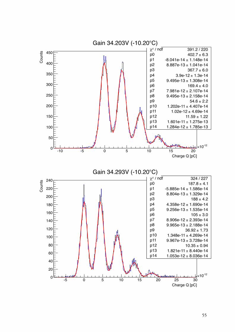
55
/ ndf 2r 391.2 / 220p0 6.3± 402.7 p1 1.148e-14± -8.041e-14 p2 1.041e-14± 8.887e-13 p3 6.0± 367.7 p4 1.3e-14± 3.9e-12 p5 1.308e-14± 9.495e-13 p6 4.0± 169.4 p7 2.107e-14± 7.981e-12 p8 2.158e-14± 9.495e-13 p9 2.2± 54.6 p10 4.407e-14± 1.202e-11 p11 4.69e-14± 1.02e-12 p12 1.22± 11.59 p13 1.275e-13± 1.601e-11 p14 1.785e-13± 1.284e-12
Charge Q [pC]-10 -5 0 5 10 15 20
-1210×
Cou
nts
0
50
100
150
200
250
300
350
400
450 / ndf 2r 391.2 / 220
p0 6.3± 402.7 p1 1.148e-14± -8.041e-14 p2 1.041e-14± 8.887e-13 p3 6.0± 367.7 p4 1.3e-14± 3.9e-12 p5 1.308e-14± 9.495e-13 p6 4.0± 169.4 p7 2.107e-14± 7.981e-12 p8 2.158e-14± 9.495e-13 p9 2.2± 54.6 p10 4.407e-14± 1.202e-11 p11 4.69e-14± 1.02e-12 p12 1.22± 11.59 p13 1.275e-13± 1.601e-11 p14 1.785e-13± 1.284e-12
C)°Gain 34.203V (-10.20
/ ndf 2r 324 / 227p0 4.1± 187.8 p1 1.586e-14± -5.885e-14 p2 1.329e-14± 8.804e-13 p3 4.2± 188 p4 1.690e-14± 4.358e-12 p5 1.535e-14± 9.256e-13 p6 3.0± 105 p7 2.393e-14± 8.906e-12 p8 2.188e-14± 9.965e-13 p9 1.73± 36.92 p10 4.269e-14± 1.348e-11 p11 3.728e-14± 9.967e-13 p12 0.94± 10.35 p13 8.440e-14± 1.821e-11 p14 8.036e-14± 1.053e-12
Charge Q [pC]-5 0 5 10 15 20 25 30
-1210×
Cou
nts
0
20
40
60
80
100
120
140
160
180
200
220
240 / ndf 2r 324 / 227p0 4.1± 187.8 p1 1.586e-14± -5.885e-14 p2 1.329e-14± 8.804e-13 p3 4.2± 188 p4 1.690e-14± 4.358e-12 p5 1.535e-14± 9.256e-13 p6 3.0± 105 p7 2.393e-14± 8.906e-12 p8 2.188e-14± 9.965e-13 p9 1.73± 36.92 p10 4.269e-14± 1.348e-11 p11 3.728e-14± 9.967e-13 p12 0.94± 10.35 p13 8.440e-14± 1.821e-11 p14 8.036e-14± 1.053e-12
C)°Gain 34.293V (-10.20

56
/ ndf 2r 305.4 / 232p0 4.2± 189.3 p1 1.49e-14± -5.37e-15 p2 1.240e-14± 8.508e-13 p3 3.7± 178.3 p4 1.803e-14± 5.382e-12 p5 1.610e-14± 1.075e-12 p6 2.71± 91.87 p7 3.139e-14± 1.076e-11 p8 3.297e-14± 1.198e-12 p9 2.47± 32.85 p10 6.165e-14± 1.607e-11 p11 7.549e-14± 1.146e-12 p12 0.606± 7.805 p13 1.071e-12± 2.074e-11 p14 1.002e-12± 4.609e-12
Charge Q [pC]-5 0 5 10 15 20 25 30
-1210×
Cou
nts
0
20
40
60
80
100
120
140
160
180
200
/ ndf 2r 305.4 / 232p0 4.2± 189.3 p1 1.49e-14± -5.37e-15 p2 1.240e-14± 8.508e-13 p3 3.7± 178.3 p4 1.803e-14± 5.382e-12 p5 1.610e-14± 1.075e-12 p6 2.71± 91.87 p7 3.139e-14± 1.076e-11 p8 3.297e-14± 1.198e-12 p9 2.47± 32.85 p10 6.165e-14± 1.607e-11 p11 7.549e-14± 1.146e-12 p12 0.606± 7.805 p13 1.071e-12± 2.074e-11 p14 1.002e-12± 4.609e-12
C)°Gain 34.402V (-10.20
/ ndf 2r 904.6 / 246p0 5.3± 252.2 p1 1.208e-14± -4.529e-14 p2 1.044e-14± 7.568e-13 p3 5.1± 252.5 p4 1.289e-14± 5.408e-12 p5 1.154e-14± 8.403e-13 p6 3.5± 125.1 p7 1.981e-14± 1.086e-11 p8 1.739e-14± 9.065e-13 p9 2.13± 48.73 p10 3.108e-14± 1.634e-11 p11 2.741e-14± 9.194e-13 p12 1.77± 14.94 p13 5.213e-14± 2.154e-11 p14 8.561e-14± 8.355e-13
Charge Q [pC]-5 0 5 10 15 20 25
-1210×
Cou
nts
0
50
100
150
200
250
300
/ ndf 2r 904.6 / 246p0 5.3± 252.2 p1 1.208e-14± -4.529e-14 p2 1.044e-14± 7.568e-13 p3 5.1± 252.5 p4 1.289e-14± 5.408e-12 p5 1.154e-14± 8.403e-13 p6 3.5± 125.1 p7 1.981e-14± 1.086e-11 p8 1.739e-14± 9.065e-13 p9 2.13± 48.73 p10 3.108e-14± 1.634e-11 p11 2.741e-14± 9.194e-13 p12 1.77± 14.94 p13 5.213e-14± 2.154e-11 p14 8.561e-14± 8.355e-13
C)°Gain 34.526V (-10.17

57
/ ndf 2r 488.3 / 164p0 15.2± 733.8 p1 1.504e-14± -8.971e-14 p2 1.544e-14± 9.333e-13 p3 11.5± 542 p4 2.815e-14± 6.973e-12 p5 3.615e-14± 1.555e-12 p6 8.6± 277.1 p7 4.759e-14± 1.422e-11 p8 4.859e-14± 1.518e-12 p9 6.95± 70.74 p10 1.165e-13± 2.169e-11 p11 1.139e-13± 1.139e-12 p12 4.6± 108 p13 1.935e-13± 1.588e-11 p14 1.260e-13± 1.012e-11
Charge Q [pC]-20 -10 0 10 20 30 40 50 60
-1210×
Cou
nts
0
100
200
300
400
500
600
700
800
/ ndf 2r 488.3 / 164p0 15.2± 733.8 p1 1.504e-14± -8.971e-14 p2 1.544e-14± 9.333e-13 p3 11.5± 542 p4 2.815e-14± 6.973e-12 p5 3.615e-14± 1.555e-12 p6 8.6± 277.1 p7 4.759e-14± 1.422e-11 p8 4.859e-14± 1.518e-12 p9 6.95± 70.74 p10 1.165e-13± 2.169e-11 p11 1.139e-13± 1.139e-12 p12 4.6± 108 p13 1.935e-13± 1.588e-11 p14 1.260e-13± 1.012e-11
C)°Gain 35.091V (-10.20
/ ndf 2r 355.5 / 157p0 13.4± 668.4 p1 1.671e-14± -1.103e-13 p2 1.578e-14± 9.896e-13 p3 8.5± 422.2 p4 4.032e-14± 7.678e-12 p5 4.285e-14± 2.156e-12 p6 7.6± 218.3 p7 7.677e-14± 1.593e-11 p8 7.356e-14± 2.265e-12 p9 6.26± 58.33 p10 1.681e-13± 2.399e-11 p11 1.902e-13± 1.676e-12 p12 5.05± 89.49 p13 2.632e-13± 1.951e-11 p14 1.747e-13± 1.101e-11
Charge Q [pC]-20 -10 0 10 20 30 40 50
-1210×
Cou
nts
0
100
200
300
400
500
600
700
/ ndf 2r 355.5 / 157p0 13.4± 668.4 p1 1.671e-14± -1.103e-13 p2 1.578e-14± 9.896e-13 p3 8.5± 422.2 p4 4.032e-14± 7.678e-12 p5 4.285e-14± 2.156e-12 p6 7.6± 218.3 p7 7.677e-14± 1.593e-11 p8 7.356e-14± 2.265e-12 p9 6.26± 58.33 p10 1.681e-13± 2.399e-11 p11 1.902e-13± 1.676e-12 p12 5.05± 89.49 p13 2.632e-13± 1.951e-11 p14 1.747e-13± 1.101e-11
C)°Gain 35.478V (-10.18

58
/ ndf 2r 205.6 / 130p0 10.8± 277.7 p1 4.832e-14± -2.069e-14 p2 4.570e-14± 1.339e-12 p3 13.8± 311.1 p4 8.546e-14± 9.969e-12 p5 1.075e-13± 2.659e-12 p6 16.1± 215.5 p7 1.312e-13± 1.944e-11 p8 1.371e-13± 2.074e-12 p9 23.9± 151.2 p10 9.21e-13± 3.62e-11 p11 3.468e-13± 1.654e-11 p12 23.3± 201.6 p13 7.429e-13± 2.792e-11 p14 8.871e-13± 1.077e-11
Charge Q [pC]-0.02 0 0.02 0.04 0.06 0.08 0.1
-910×
Cou
nts
0
50
100
150
200
250
300
350
400
450
/ ndf 2r 205.6 / 130p0 10.8± 277.7 p1 4.832e-14± -2.069e-14 p2 4.570e-14± 1.339e-12 p3 13.8± 311.1 p4 8.546e-14± 9.969e-12 p5 1.075e-13± 2.659e-12 p6 16.1± 215.5 p7 1.312e-13± 1.944e-11 p8 1.371e-13± 2.074e-12 p9 23.9± 151.2 p10 9.21e-13± 3.62e-11 p11 3.468e-13± 1.654e-11 p12 23.3± 201.6 p13 7.429e-13± 2.792e-11 p14 8.871e-13± 1.077e-11
C)°Gain 36.030V (-10.17

59
9.2.2 Histogram fits to determine gain for 100A (chapter 5.1)
/ ndf 2r 703.3 / 316p0 5.2± 490.9 p1 4.000e-15± -3.438e-13 p2 3.379e-15± 4.898e-13 p3 2.3± 110.6 p4 8.920e-15± 3.676e-12 p5 7.479e-15± 5.494e-13 p6 0.78± 12.18 p7 3.076e-14± 7.747e-12 p8 3.017e-14± -6.219e-13
Charge Q [pC]-2 0 2 4 6 8 10 12
-1210×
Cou
nts
0
100
200
300
400
500
/ ndf 2r 703.3 / 316p0 5.2± 490.9 p1 4.000e-15± -3.438e-13 p2 3.379e-15± 4.898e-13 p3 2.3± 110.6 p4 8.920e-15± 3.676e-12 p5 7.479e-15± 5.494e-13 p6 0.78± 12.18 p7 3.076e-14± 7.747e-12 p8 3.017e-14± -6.219e-13
Charge: 4.03253e-12 CGain: 251719
C)°Gain 35.51V ( T = -8.61
/ ndf 2r 943 / 227p0 8.5± 621.2 p1 4.900e-15± -3.553e-13 p2 3.645e-15± 4.454e-13 p3 3.9± 138.7 p4 1.125e-14± 4.017e-12 p5 1.081e-14± 5.713e-13 p6 1.45± 18.69 p7 3.935e-14± 8.416e-12 p8 4.522e-14± 7.213e-13
Charge Q [pC]-5 0 5 10 15 20
-1210×
Cou
nts
0
100
200
300
400
500
600
/ ndf 2r 943 / 227p0 8.5± 621.2 p1 4.900e-15± -3.553e-13 p2 3.645e-15± 4.454e-13 p3 3.9± 138.7 p4 1.125e-14± 4.017e-12 p5 1.081e-14± 5.713e-13 p6 1.45± 18.69 p7 3.935e-14± 8.416e-12 p8 4.522e-14± 7.213e-13
Charge: 4.37928e-12 CGain: 273363
C)°Gain 35.60V ( T = -8.55

60
/ ndf 2r 264.9 / 157p0 7.8± 580.4 p1 4.889e-15± -3.756e-13 p2 3.182e-15± 4.203e-13 p3 3.8± 147.6 p4 1.075e-14± 4.611e-12 p5 7.981e-15± 5.112e-13 p6 1.47± 19.68 p7 2.995e-14± 9.649e-12 p8 2.516e-14± 5.092e-13
Charge Q [pC]-5 0 5 10 15 20
-1210×
Cou
nts
0
100
200
300
400
500
600 / ndf 2r 264.9 / 157p0 7.8± 580.4 p1 4.889e-15± -3.756e-13 p2 3.182e-15± 4.203e-13 p3 3.8± 147.6 p4 1.075e-14± 4.611e-12 p5 7.981e-15± 5.112e-13 p6 1.47± 19.68 p7 2.995e-14± 9.649e-12 p8 2.516e-14± 5.092e-13
Charge: 4.9995e-12 CGain: 312078
C)°Gain 35.69V ( T = -8.58
/ ndf 2r 311.9 / 160p0 8.3± 666.9 p1 4.624e-15± -3.578e-13 p2 3.00e-15± 4.26e-13 p3 4.1± 180.9 p4 9.741e-15± 5.287e-12 p5 6.612e-15± 5.065e-13 p6 1.61± 30.18 p7 2.740e-14± 1.097e-11 p8 2.192e-14± 5.991e-13
Charge Q [pC]0 5 10 15 20
-1210×
Cou
nts
0
100
200
300
400
500
600
700 / ndf 2r 311.9 / 160p0 8.3± 666.9 p1 4.624e-15± -3.578e-13 p2 3.00e-15± 4.26e-13 p3 4.1± 180.9 p4 9.741e-15± 5.287e-12 p5 6.612e-15± 5.065e-13 p6 1.61± 30.18 p7 2.740e-14± 1.097e-11 p8 2.192e-14± 5.991e-13
Charge: 5.65414e-12 CGain: 352943
C)°Gain 35.80V ( T = -8.55

61
/ ndf 2r 1478 / 288p0 7.6± 505.1 p1 5.516e-15± -3.812e-13 p2 4.428e-15± 4.668e-13 p3 3.3± 124.5 p4 1.38e-14± 6.09e-12 p5 1.32e-14± 7.13e-13 p6 1.06± 18.49 p7 4.168e-14± 1.263e-11 p8 3.737e-14± 9.527e-13
Charge Q [pC]-5 0 5 10 15 20 25
-1210×
Cou
nts
0
100
200
300
400
500
/ ndf 2r 1478 / 288p0 7.6± 505.1 p1 5.516e-15± -3.812e-13 p2 4.428e-15± 4.668e-13 p3 3.3± 124.5 p4 1.38e-14± 6.09e-12 p5 1.32e-14± 7.13e-13 p6 1.06± 18.49 p7 4.168e-14± 1.263e-11 p8 3.737e-14± 9.527e-13
Charge: 6.48725e-12 CGain: 404947
C)°Gain 35.91V ( T = -8.55
/ ndf 2r 1304 / 324p0 3.2± 251 p1 1.246e-14± -1.392e-12 p2 9.209e-15± 1.193e-12 p3 1.90± 94.23 p4 2.163e-14± 5.592e-12 p5 1.58e-14± 1.27e-12 p6 0.81± 18.17 p7 5.353e-14± 1.263e-11 p8 4.124e-14± 1.384e-12
Charge Q [pC]-5 0 5 10 15 20
-1210×
Cou
nts
0
50
100
150
200
250
300
/ ndf 2r 1304 / 324p0 3.2± 251 p1 1.246e-14± -1.392e-12 p2 9.209e-15± 1.193e-12 p3 1.90± 94.23 p4 2.163e-14± 5.592e-12 p5 1.58e-14± 1.27e-12 p6 0.81± 18.17 p7 5.353e-14± 1.263e-11 p8 4.124e-14± 1.384e-12
Charge: 6.99845e-12 CGain: 436857
C)°Gain 36.02V ( T = -8.52

62
/ ndf 2r 373.1 / 233p0 6.0± 419 p1 6.649e-15± -5.459e-13 p2 4.847e-15± 5.652e-13 p3 3.0± 138.2 p4 1.277e-14± 6.952e-12 p5 9.304e-15± 6.905e-13 p6 1.30± 24.31 p7 3.538e-14± 1.436e-11 p8 3.234e-14± 8.363e-13
Charge Q [pC]0 5 10 15 20
-1210×
Cou
nts
0
50
100
150
200
250
300
350
400
450 / ndf 2r 373.1 / 233p0 6.0± 419 p1 6.649e-15± -5.459e-13 p2 4.847e-15± 5.652e-13 p3 3.0± 138.2 p4 1.277e-14± 6.952e-12 p5 9.304e-15± 6.905e-13 p6 1.30± 24.31 p7 3.538e-14± 1.436e-11 p8 3.234e-14± 8.363e-13
Charge: 7.47422e-12 CGain: 466556
C)°Gain 36.11V ( T = -8.51
/ ndf 2r 317.3 / 215p0 5.7± 383.9 p1 6.777e-15± -6.093e-13 p2 4.521e-15± 5.485e-13 p3 3.2± 135.8 p4 1.242e-14± 7.326e-12 p5 8.56e-15± 6.51e-13 p6 1.54± 31.34 p7 2.765e-14± 1.524e-11 p8 2.235e-14± -7.088e-13
Charge Q [pC]-5 0 5 10 15 20 25 30
-1210×
Cou
nts
0
50
100
150
200
250
300
350
400 / ndf 2r 317.3 / 215p0 5.7± 383.9 p1 6.777e-15± -6.093e-13 p2 4.521e-15± 5.485e-13 p3 3.2± 135.8 p4 1.242e-14± 7.326e-12 p5 8.56e-15± 6.51e-13 p6 1.54± 31.34 p7 2.765e-14± 1.524e-11 p8 2.235e-14± -7.088e-13
Charge: 7.93102e-12 CGain: 495070
C)°Gain 36.20V ( T = -8.45

63
/ ndf 2r 249.7 / 117p0 14.6± 971.3 p1 6.80e-15± -7.01e-13 p2 4.973e-15± 5.564e-13 p3 7.8± 328 p4 1.290e-14± 7.911e-12 p5 9.533e-15± 6.778e-13 p6 3.49± 73.39 p7 2.890e-14± 1.645e-11 p8 2.116e-14± 7.401e-13
Charge Q [pC]0 10 20 30 40 50
-1210×
Cou
nts
0
200
400
600
800
1000 / ndf 2r 249.7 / 117p0 14.6± 971.3 p1 6.80e-15± -7.01e-13 p2 4.973e-15± 5.564e-13 p3 7.8± 328 p4 1.290e-14± 7.911e-12 p5 9.533e-15± 6.778e-13 p6 3.49± 73.39 p7 2.890e-14± 1.645e-11 p8 2.116e-14± 7.401e-13
Charge: 8.59343e-12 CGain: 536419
C)°Gain 36.31V ( T = -8.43
/ ndf 2r 806.9 / 321p0 5.5± 335.1 p1 7.602e-15± -6.041e-13 p2 6.303e-15± 6.013e-13 p3 2.8± 112.7 p4 1.529e-14± 8.859e-12 p5 1.356e-14± 8.134e-13 p6 1.25± 24.87 p7 3.634e-14± 1.821e-11 p8 3.510e-14± 9.707e-13
Charge Q [pC]0 5 10 15 20 25 30
-1210×
Cou
nts
0
50
100
150
200
250
300
350
/ ndf 2r 806.9 / 321p0 5.5± 335.1 p1 7.602e-15± -6.041e-13 p2 6.303e-15± 6.013e-13 p3 2.8± 112.7 p4 1.529e-14± 8.859e-12 p5 1.356e-14± 8.134e-13 p6 1.25± 24.87 p7 3.634e-14± 1.821e-11 p8 3.510e-14± 9.707e-13
Charge: 9.43466e-12 CGain: 588930
C)°Gain 36.42V ( T = -8.48

64
/ ndf 2r 488.5 / 174p0 10.6± 657.8 p1 1.040e-14± -2.016e-12 p2 9.219e-15± 8.637e-13 p3 5.9± 273 p4 1.756e-14± 7.974e-12 p5 1.37e-14± 1.01e-12 p6 2.7± 66.3 p7 3.869e-14± 1.779e-11 p8 3.218e-14± 1.205e-12
Charge Q [pC]0 10 20 30 40 50
-1210×
Cou
nts
0
100
200
300
400
500
600
700
/ ndf 2r 488.5 / 174p0 10.6± 657.8 p1 1.040e-14± -2.016e-12 p2 9.219e-15± 8.637e-13 p3 5.9± 273 p4 1.756e-14± 7.974e-12 p5 1.37e-14± 1.01e-12 p6 2.7± 66.3 p7 3.869e-14± 1.779e-11 p8 3.218e-14± 1.205e-12
Charge: 9.94733e-12 CGain: 620932
C)°Gain 36.51V ( T = -8.62
/ ndf 2r 622.7 / 204p0 12.0± 835.8 p1 8.381e-15± -4.429e-13 p2 5.965e-15± 7.106e-13 p3 6.7± 328 p4 1.486e-14± 1.172e-11 p5 1.111e-14± 8.915e-13 p6 3.08± 86.43 p7 3.280e-14± 2.346e-11 p8 2.496e-14± 1.144e-12
Charge Q [pC]0 10 20 30 40 50 60
-1210×
Cou
nts
0
100
200
300
400
500
600
700
800
/ ndf 2r 622.7 / 204p0 12.0± 835.8 p1 8.381e-15± -4.429e-13 p2 5.965e-15± 7.106e-13 p3 6.7± 328 p4 1.486e-14± 1.172e-11 p5 1.111e-14± 8.915e-13 p6 3.08± 86.43 p7 3.280e-14± 2.346e-11 p8 2.496e-14± 1.144e-12
Charge: 1.20597e-11 CGain: 752791
C)°Gain 36.97V ( T = -8.46

65
/ ndf 2r 969.6 / 282p0 9.9± 568.4 p1 1.096e-14± -9.608e-13 p2 1.018e-14± 8.481e-13 p3 5.1± 230.5 p4 1.979e-14± 1.461e-11 p5 1.637e-14± 1.166e-12 p6 2.16± 66.54 p7 4.288e-14± 2.896e-11 p8 3.125e-14± 1.581e-12
Charge Q [pC]0 10 20 30 40 50 60 70
-1210×
Cou
nts
0
100
200
300
400
500
600 / ndf 2r 969.6 / 282
p0 9.9± 568.4 p1 1.096e-14± -9.608e-13 p2 1.018e-14± 8.481e-13 p3 5.1± 230.5 p4 1.979e-14± 1.461e-11 p5 1.637e-14± 1.166e-12 p6 2.16± 66.54 p7 4.288e-14± 2.896e-11 p8 3.125e-14± 1.581e-12
Charge: 1.52632e-11 CGain: 952762
C)°Gain 37.50V ( T = -8.41
/ ndf 2r 1883 / 211p0 20.0± 1423 p1 1.14e-14± -8.45e-13 p2 1.130e-14± 1.137e-12 p3 10.7± 611.5 p4 2.012e-14± 1.729e-11 p5 1.654e-14± 1.448e-12 p6 4.6± 172.8 p7 4.953e-14± 3.332e-11 p8 3.935e-14± 2.304e-12
Charge Q [pC]0 0.02 0.04 0.06 0.08 0.1
-910×
Cou
nts
0
200
400
600
800
1000
1200
1400
1600 / ndf 2r 1883 / 211
p0 20.0± 1423 p1 1.14e-14± -8.45e-13 p2 1.130e-14± 1.137e-12 p3 10.7± 611.5 p4 2.012e-14± 1.729e-11 p5 1.654e-14± 1.448e-12 p6 4.6± 172.8 p7 4.953e-14± 3.332e-11 p8 3.935e-14± 2.304e-12
Charge: 1.76075e-11 CGain: 1.09909e+06
C)°Gain 38.04V ( T = -8.44

66
/ ndf 2r 1280 / 352p0 7.0± 365.8 p1 1.672e-14± -1.172e-12 p2 1.614e-14± 1.174e-12 p3 3.5± 146.6 p4 2.853e-14± 1.988e-11 p5 2.30e-14± 1.53e-12 p6 1.46± 39.59 p7 9.451e-14± 3.788e-11 p8 8.325e-14± 2.945e-12
Charge Q [pC]0 10 20 30 40 50 60 70
-1210×
Cou
nts
0
50
100
150
200
250
300
350
400
450 / ndf 2r 1280 / 352p0 7.0± 365.8 p1 1.672e-14± -1.172e-12 p2 1.614e-14± 1.174e-12 p3 3.5± 146.6 p4 2.853e-14± 1.988e-11 p5 2.30e-14± 1.53e-12 p6 1.46± 39.59 p7 9.451e-14± 3.788e-11 p8 8.325e-14± 2.945e-12
Charge: 2.02877e-11 CGain: 1.2664e+06
C)°Gain 38.50V ( T = -8.47
/ ndf 2r 1397 / 370p0 7.0± 390.3 p1 1.715e-14± -9.134e-13 p2 1.341e-14± 1.136e-12 p3 3.7± 152.1 p4 3.083e-14± 2.218e-11 p5 2.355e-14± 1.523e-12 p6 1.06± 25.36 p7 2.324e-13± 4.364e-11 p8 2.210e-13± 6.095e-12
Charge Q [pC]0 10 20 30 40 50 60 70
-1210×
Cou
nts
0
50
100
150
200
250
300
350
400
/ ndf 2r 1397 / 370p0 7.0± 390.3 p1 1.715e-14± -9.134e-13 p2 1.341e-14± 1.136e-12 p3 3.7± 152.1 p4 3.083e-14± 2.218e-11 p5 2.355e-14± 1.523e-12 p6 1.06± 25.36 p7 2.324e-13± 4.364e-11 p8 2.210e-13± 6.095e-12
Charge: 2.26836e-11 CGain: 1.41595e+06
C)°Gain 39.00V ( T = -8.40

67
/ ndf 2r 1331 / 277p0 11.1± 622.9 p1 2.223e-14± -1.289e-12 p2 1.949e-14± 1.564e-12 p3 5.9± 251.8 p4 3.727e-14± 2.406e-11 p5 2.96e-14± 1.96e-12 p6 1.81± 60.68 p7 1.877e-13± 4.605e-11 p8 1.703e-13± 6.981e-12
Charge Q [pC]0 0.02 0.04 0.06 0.08 0.1 0.12 0.14
-910×
Cou
nts
0
100
200
300
400
500
600
700 / ndf 2r 1331 / 277
p0 11.1± 622.9 p1 2.223e-14± -1.289e-12 p2 1.949e-14± 1.564e-12 p3 5.9± 251.8 p4 3.727e-14± 2.406e-11 p5 2.96e-14± 1.96e-12 p6 1.81± 60.68 p7 1.877e-13± 4.605e-11 p8 1.703e-13± 6.981e-12
Charge: 2.45089e-11 CGain: 1.52989e+06
C)°Gain 39.51V ( T = -8.42

68
9.2.3 Crosstalk evaluation plots (chapter 5.2)
/ ndf 2r 718.5 / 325p0 1.7± 146.7 p1 6.066e-15± 3.752e-12 p2 4.945e-15± 6.566e-13
Charge Q [pC]1 2 3 4 5 6 7 8 9
-1210×
Cou
nts
0
20
40
60
80
100
120
140
160
180
200 / ndf 2r 718.5 / 325
p0 1.7± 146.7 p1 6.066e-15± 3.752e-12 p2 4.945e-15± 6.566e-13
Crosstalk: 1.02789%
C)°Crosstalk 35.51V ( T = -8.61
/ ndf 2r 1041 / 230p0 5.6± 535.9 p1 3.98e-15± 6.79e-12 p2 3.848e-15± 5.297e-13
Charge Q [pC]2 4 6 8 10 12 14 16 18 20
-1210×
Cou
nts
0
100
200
300
400
500
600
/ ndf 2r 1041 / 230p0 5.6± 535.9 p1 3.98e-15± 6.79e-12 p2 3.848e-15± 5.297e-13
Crosstalk: 2.78462%
C)°Crosstalk 36.02V ( T = -8.50

69
/ ndf 2r 1264 / 191p0 11.7± 1284 p1 3.418e-15± 9.194e-12 p2 2.570e-15± 4.669e-13
Charge Q [pC]5 10 15 20 25 30
-1210×
Cou
nts
0
200
400
600
800
1000
1200
/ ndf 2r 1264 / 191p0 11.7± 1284 p1 3.418e-15± 9.194e-12 p2 2.570e-15± 4.669e-13
Crosstalk: 5.74013%
C)°Crosstalk 36.50V ( T = -8,82
/ ndf 2r 2573 / 252p0 7.8± 845.6 p1 5.010e-15± 1.392e-11 p2 3.501e-15± 6.557e-13
Charge Q [pC]10 15 20 25 30 35 40
-1210×
Cou
nts
0
100
200
300
400
500
600
700
800
900 / ndf 2r 2573 / 252p0 7.8± 845.6 p1 5.010e-15± 1.392e-11 p2 3.501e-15± 6.557e-13
Crosstalk: 13.8045%
C)°Crosstalk 37.50V ( T = -8.75

70
/ ndf 2r 2986 / 251p0 19.5± 1820 p1 5.130e-15± 1.685e-11 p2 3.875e-15± 6.018e-13
Charge Q [pC]10 20 30 40 50 60 70 80
-1210×
Cou
nts
0
200
400
600
800
1000
1200
1400
1600
1800 / ndf 2r 2986 / 251
p0 19.5± 1820 p1 5.130e-15± 1.685e-11 p2 3.875e-15± 6.018e-13
Crosstalk: 19.3817%
C)°Crosstalk 38.08V ( T = -8.47
/ ndf 2r 3654 / 330p0 15.2± 1163 p1 6.744e-15± 2.123e-11 p2 5.410e-15± 6.615e-13
Charge Q [pC]10 20 30 40 50 60 70 80
-1210×
Cou
nts
0
200
400
600
800
1000
1200 / ndf 2r 3654 / 330
p0 15.2± 1163 p1 6.744e-15± 2.123e-11 p2 5.410e-15± 6.615e-13
Crosstalk: 31.1131%
C)°Crosstalk 39.01V ( T = -8.47

71
/ ndf 2r 6556 / 361p0 15.8± 1420 p1 6.519e-15± 2.345e-11 p2 5.240e-15± 7.539e-13
Charge Q [pC]10 20 30 40 50 60 70
-1210×
Cou
nts
0
200
400
600
800
1000
1200
1400
/ ndf 2r 6556 / 361p0 15.8± 1420 p1 6.519e-15± 2.345e-11 p2 5.240e-15± 7.539e-13
Crosstalk: 37.2347%
C)°Crosstalk 39.53V ( T = -8.43
/ ndf 2r 7698 / 229p0 27.7± 2325 p1 7.682e-15± 2.498e-11 p2 6.571e-15± 8.474e-13
Charge Q [pC]0.02 0.04 0.06 0.08 0.1
-910×
Cou
nts
0
500
1000
1500
2000
2500 / ndf 2r 7698 / 229p0 27.7± 2325 p1 7.682e-15± 2.498e-11 p2 6.571e-15± 8.474e-13
Crosstalk: 44.2319%
C)°Crosstalk 39.98V ( T = -8.44

72
9.2.4 PDE evaluation plots (chapter 5.3.3)
Charge Q [pC]0 0.02 0.04 0.06 0.08 0.1 0.12 0.14
-910×
Cou
nts
0
50
100
150
200
250 PDE @ 375nm: 6.18959%
C)°PDE @ 375nm (V = 38.50V, T = -8.42
Charge Q [pC]0 0.02 0.04 0.06 0.08 0.1 0.12 0.14
-910×
Cou
nts
0
50
100
150
200
250PDE @ 375nm: 6.19852%
C)°PDE @ 375nm Switch (V = 38.50V, T = -8.43

73
Charge Q [pC]-0.02 0 0.02 0.04 0.06 0.08 0.1 0.12
-910×
Cou
nts
0
50
100
150
200
250
300
350
400
450PDE @ 405nm: 12.0105%
C)°PDE @ 405nm (V = 38.50V, T = -8.38
Charge Q [pC]0 0.02 0.04 0.06 0.08 0.1 0.12 0.14
-910×
Cou
nts
0
50
100
150
200
250
300
350
400
450
PDE @ 450nm: 17.9943%
C)°PDE @ 450nm (V = 38.50V, T = -8.40

74
9.3 Filter Transmission Table

75
9.4 Pi Filter Frequency Response Simulation


Acknowledgment First of all I want to thank Masahiro Teshima that he gave me around two years ago the chance to follow my dream and participate in astronomic research at the Magic Group. All along this period Razmik Mirzoyan was responsible for my work and myself at the Max Planck Institute. He gave me the freedom to realize my own ideas, to make mistakes and learn from them. Also, he always took the time and sacrificed his holidays to support me with problems regarding my work and to give me little lectures in basic physics and introduction to astro-particle physics. I enjoyed that really much and I’m so grateful for that. As well I would like to thank Jürgen Hose who always gave me good advice and supported me with technical issues. Moreover he helped me conduct innumerable measurements and experiments and deal with all the little problems that occur in everyday lab life. Gratitude I owe also my colleagues Matthias Kurz, Christian Fruck, Dennis Häfner, Hanna Kellermann, Florian Frank (especially for taking all the pictures) and Max Knötig who supported me in solving fiddly tasks and made the time at the MPP so memorable. It was a pleasure and a lot fun to work with these guys. Furthermore I need to acknowledge Reinhard Kastner and all the apprentices from the mechanics facility, Si Tran, Ronald Maier and Christoph Knust from the electrical department and all the other employees of the MPP for bringing my sketches and visions to life (even though they were not always simple) and supporting me in every way. Special thanks also to my Prof. Dr. Rolf Heilmann who supervised my Thesis at the University of Applied Sciences Munich. Finally, but not at all less thankful I am to my parents who made it possible for me to reach this point and who supported me all the way during my studies.


Declaration of Authorship I certify that the work presented here is, to the best of my knowledge and belief, original and the result of my own investigations, except as acknowledged, and has not been submitted, either in part or whole, for a degree at this or any other university. Hiermit versichere ich eidesstattlich, dass ich die vorliegende Arbeit selbständig und ohne Benutzung anderer als der angegebenen Hilfsmittel angefertigt habe. Alle Stellen, die wörtlich oder sinngemäß aus Veröffentlichungen entnommen sind, wurden als solche kenntlich gemacht. Dies gilt auch für Zeichnungen, Skizzen, bildliche Darstellungen sowie für Quellen aus dem Internet. Die Arbeit wurde in gleicher oder ähnlicher Form keiner anderen Prüfungsbehörde vorgelegt. München, den 5. September 2011 Toni Engelhardt Matrikelnr.: 13573407