DEVELOPMENT OF A 60 W PULSED FIBER LASER AMPLIFIER...
134
DEVELOPMENT OF A 60 W PULSED FIBER LASER AMPLIFIER FOR MATERIALS PROCESSING A THESIS SUBMITTED TO THE GRADUATE SCHOOL OF NATURAL AND APPLIED SCIENCES OF MIDDLE EAST TECHNICAL UNIVERSITY BY YİĞİT OZAN AYDIN IN PARTIAL FULFILLMENT OF THE REQUIREMENTS FOR THE DEGREE OF MASTER OF SCIENCE IN MICRO AND NANOTECHNOLOGY JUNE 2014
Transcript of DEVELOPMENT OF A 60 W PULSED FIBER LASER AMPLIFIER...
DEVELOPMENT OF A 60 W PULSED FIBER
LASER AMPLIFIER FOR MATERIALS PROCESSING
A THESIS SUBMITTED TO
THE GRADUATE SCHOOL OF NATURAL AND APPLIED SCIENCES
OF
MIDDLE EAST TECHNICAL UNIVERSITY
BY
YİĞİT OZAN AYDIN
IN PARTIAL FULFILLMENT OF THE REQUIREMENTS
FOR
THE DEGREE OF MASTER OF SCIENCE
IN
MICRO AND NANOTECHNOLOGY
JUNE 2014


Approval of the Thesis:
DEVELOPMENT OF A 60 W PULSED FIBER
LASER AMPLIFIER FOR MATERIALS PROCESSING
Submitted by YİĞİT OZAN AYDIN in partial fulfillment of the requirements for the
degree of Master of Science in Micro and Nanotechnology Department, Middle East
Technical University by,
Prof. Dr. Canan Özgen
Dean, Graduate School of Natural and Applied Sciences ________________
Prof. Dr. Tayfun Akın
Head of Department, Micro and Nanotechnology
________________
Assist. Prof. Dr. Alpan Bek
Supervisor, Physics Dept., METU
________________
Assoc. Prof. Dr. Asaf Behzat Şahin
Co-Supervisor, Electronics and Communications Eng., YBU
________________
Examining Committee Members:
Prof. Dr. Raşit Turan
Physics Dept., METU
________________
Assist. Prof. Dr. Alpan Bek
Physics Dept., METU
________________
Assoc. Prof. Dr. F.Ömer İlday
Physics Dept., Bilkent Univ.
________________
Assist. Prof. Dr. Halil Berberoğlu
Physics Dept., Gazi Univ.
________________
Koray Eken, M. Sc.
FiberLAST Inc.
________________
Date: 30.06.2014

iv
I hereby declare that all information in this document has been obtained and presented in accordance with academic rules and ethical conduct. I also declare that, as required by these rules and conduct, I have fully cited and referenced all
material and results that are not original to this work.
Name, Last name : Yiğit Ozan Aydın
Signature :

v
ABSTRACT
DEVELOPMENT OF A 60 W PULSED FIBER
LASER AMPLIFIER FOR MATERIALS PROCESSING
Aydın, Yiğit Ozan
M. Sc. Department of Micro and Nanotechnology
Supervisor: Assist. Prof. Dr. AlpanBek
Co-Supervisor: Assoc. Prof. Dr. Asaf Behzat Şahin
June 2014, 116 pages
Fiber lasers have the advantage of high beam quality, high efficiency, small
size, air cooling and therefore much interest in the development of high power fiber laser
systems have arisen recently in the world. Almost all commercially developed fiber lasers
with nanosecond pulse duration, that are being used for material processing, are Q-switched
systems. Vital parameters in the material processing such as repetition rate, pulse energy and
pulse duration are correlated with each other and they cannot be adjusted independently
in the Q-switch mechanism.
In this study, ytterbium doped all-fiber laser amplifier with 60 W average power
and more than 20 kW peak power at 1 µm wavelength was developed, and its potential for
processing of different material types is investigated. This master-oscillator power-
amplifier (MOPA) architectured system is composed of pulses, produced by an
electronically pumped diode, and amplified by a series of fiber amplifiers. In contrast with
Q-switch lasers, MOPA architecture allows us to adjust pulse duration, repetition rate and
power independently. Beam quality is nearly diffraction limited, and the typical M2 value
is1.5. The system is an all-fiber one where the maximum pulse energy achieved at 100
kHz repetition rate is 0.6 mJ and minimum pulse duration is ~30 ns at this energy level.
Due to multi-stage architecture and special precautions, the system works without a high
amplified spontaneous emission (ASE) level and shows an optical efficiency of 76%. After
development of the laser amplifier, and certification of its materials processing capability,
an industrial prototype was configured by taking the cost-efficiency into account . The laser
components were placed into a compact case which has a simple design for thermal

vi
cooling. The developed industrial laser amplifier prototype has several unique properties
with respect to other equivalent MOPA design fiber lasers.
In material processing, high stability and high beam quality lead to high
consistency. Reduced diameters of active and passive fiber cores and specially optimized
fiber splices, which are used in the system architecture, result with higher beam quality thus
the focusing is superior to many contemporary commercial lasers. As the intensity (areal
power density) is the physical quantity that drives the nature of interaction of laser output
with materials, the developed system offers long operation life-time due to its capability of
operation at lower power levels than its contemporaries.
In order to demonstrate the efficiency and the ability of processing various different
kinds of materials with the developed laser amplifier system, a multitude of processing
applications such as micro drilling, solar cell edge isolation, deep engraving and color
marking were tested on metal, semiconductor and insulator surfaces and the results are
discussing in relationship with various system operation parameters.
Keywords : fiber laser, materials processing, pulsed lasers, ytterbium laser, MOPA
lasers

vii
ÖZ
MALZEME İŞLEME İÇİN 60 W DARBELİ FİBER
LAZER YÜKSELTECİ GELİŞTİRİLMESİ
Aydın, Yiğit Ozan
Yüksek Lisans, Mikro ve Nanoteknoloji Bölümü
Tez Yöneticisi: Yard. Doç. Dr. Alpan Bek
Ortak Tez Yöneticisi: Doç. Dr. Asaf Behzat Şahin
Haziran 2014, 116 sayfa
Günümüzde fiber lazer teknolojisi, uygulamalı fiziğin en hızlı gelişen alanlarından
bir tanesidir. Kompakt olarak tasarlanabilmesi, esnek ve taşınabilirliği, yüksek ışın kalitesi,
hassas malzeme işleme kabiliyeti, yüksek verimlilikte çalışması, su ile soğutma
gerektirmemesi, düşük bakım maliyetine sahip olması gibi önemli pratik avantajları bu
gelişmedeki en önemli etkenler arasındadır. Endüstriyel olarak geliştirilen ve malzeme
işlemek için kullanılan nanosaniye mertebesindeki darbelere sahip fiber lazer sistemlerinin
neredeyse tamamına yakını Q-Switch konfigürasyonuna sahiptir. Malzeme işleme
uygulamalarındaki tekrar frekansı, darbe enerjisi ve darbe süresi gibi önemli parametreler
Q-Switch sistemlerde birbirinden bağımsız olarak ayarlanamamaktadır.
Bu çalışmada malzeme işleme uygulamalarında kullanılmak üzere, iterbiyum katkılı,
tümleşik, 60 W ortalama güce ve 20 kW’dan fazla tepe gücüne sahip, 1 µm dalga boyunda
çalışan bir lazer kaynağı geliştirilmiş, lazerin çeşitli malzemeler üzerindeki etkisi
incelenmiştir. MOPA mimarisi ile tasarlanan sistemde elektronik olarak modüle edilen bir
lazer diyod aracılığıyla üretilen darbeler, tasarlanan yükselteçlerle bir kaç mW güç
seviyesinden 60 W ortalama güce çıkartılmıştır. Q-Switch tasarımdan farklı olarak MOPA
mimarisi bizlere darbe süresinin tekrar frekansından ve ortalama güçten bağımsız olarak
ayarlanabilmesi imkanını vermiştir. Sistemden elde edilen lazerin ışın kalitesi neredeyse
kırınımla sınırlı olup M2 ~ 1,5 seviyelerindedir. Sistem, fiberle tümleşik ve 100 kHz tekrar
freakansında 0.6 mJ darbe enerjisine sahip olup, minimum 30 ns’ye kadar darbe süresine

viii
sahip lazer ışını üretebilmektedir. Çok kademeli tasarım sayesinde kendiliğinden
yükseltilmiş ışıma (amplified spontaneous emission) baskılanmış ve son yükselteçte %76
optik verimlilik elde edilmiştir. Lazer yükselticinin geliştirilme aşamasının ardından, uygun
maliyetlilik göz önüne alınarak sistemin endüstriyelleşmesi sağlanmıştır. Lazerin
yükseltecinin oluşturulması sırasında kullanılan komponentler termal etkileri azaltabilecek
şekilde dizayn edilen kompakt bir yapı içerisinde muhafaza edilerek son ürün haline
getirilmiştir. Geliştirilen fiber lazer yükselteci, muadillerine göre birçok özgün özellik
barındırmaktadır.
Lazerle malzeme işleme uygulamalarında, yüksek kararlılık ve ışın kalitesi verimli
işleme sonuçlarını kullanıcıyı sağlamaktadır. Düşük çekirdek yarıçaplı aktif ve pasif fiberler
ve optimizasyonu yapılan fiber kaynakları ile elde edilen yüksek ışın kalitesi ile iyi bir
odaklama imkanı sağlanmıştır. Malzeme ve lazer etkileşiminde, gücün etki ettiği alan
(yoğunluk) işlemin sonucunu belirleyen yegane unsurlardan birisi olup, yüksek ışın kalitesi
ile küçük bir alana etki malze işleme kalitesini arttırmaktadır.
Sistemin farklı malzemeler üzerindeki işleme verimliliğini ve yeteneğini anlamak
için mikrodelme, güneş hücresi kenar izolasyonu, derin kazıma ve renkli markalama gibi
uygulamalar gerçekleştirilip lazer parametrelerinin bu uygulamalar üzerindeki etkisi
tartışılmıştır.
Anahtar kelimeler : fiber lazer, malzeme işleme, darbeli lazerler, iterbiyum fiber lazer,
MOPA lazer

ix
to all my family…

x
ACKNOWLEDGEMENTS
First and foremost, I would like to thank my supervisor Assist. Prof. Dr. Alpan Bek, who
have provided me guidance, enlightened and motivated me with his immense knowledge
and enthusiasm.
I am very grateful to FiberLAST Inc., especially company manager Koray Eken who
provided me a great laboratory and support throughout the production of my thesis.
Very special thanks to my colleagues Emre Yağcı , Sarper Salman, Mesut Tasalı, Seydi
Yavaş for assisting and helping me in the development of fiber laser part of this study.
I would like to thank F.Ömer İlday who guided me with his precious suggestions for
maturing my ideas and opinions.
Very special thanks to Fırat Es, Mona Zolfaghari Borra, Yusuf Kasap which assisted and
helped me in the materials processing applications part of this study.
I am greatly indebted to my family; in particular to my mother Alev Aydın, my father Hasan
Aydın, my brother Ahmet Can Aydın, my aunt Ayfer Gündoğan, my uncle Atila Cindemir
for their unconditional love and limitless patience. Also I would like to thank Tolga Tezcan,
Onur Kara, Hasan Mert Bozacı, Levent Öztürk, Murat Çalık and Berçin Pınar for their
friendship, special effort and interest during this thesis period.

xi
TABLE OF CONTENTS
ABSTRACT ........................................................................................................................... v
ÖZ .............................................................................................................................. vii
ACKNOWLEDGEMENTS ......................................................................................... x
LIST OF TABLES .................................................................................................... xiii
LIST OF FIGURES .................................................................................................. xiv
CHAPTERS
1. INTRODUCTION ................................................................................................... 1
1.1 Brief History and Evolution of Fiber Lasers and Amplifiers ......................................... 1
1.2 Laser Material Proccessing .............................................................................................. 4
2. THE OPERATION PRINCIPLES OF FIBER LASER COMPONENTS ............... 7
2.1 Theory of Fiber Lasers and Amplifiers ........................................................................... 7
2.1.1 Optical Fibers ................................................................................................................. 7
2.1.2 Ytterbium Doped Silica Fibers ................................................................................... 10
2.1.3 Double-Clad Fibers ..................................................................................................... 12
2.1.4 Large Mode Area Fibers ............................................................................................. 13
2.1.5 Gain and Laser Amplification ..................................................................................... 13
2.1.6 Limitations of the amplifier ......................................................................................... 17
2.1.7 Amplified Spontaneous Emission .............................................................................. 20
2.1.8 Master Oscillator Power Amplifier (MOPA) Configuration .................................... 21
3. PHYSICAL MECHANISM BEHIND LASER MATERIAL PROCESSING ...... 23
3.1 Physical Processes .......................................................................................................... 25
3.1.1 Heating ......................................................................................................................... 29
3.1.2 Melting ......................................................................................................................... 31
3.1.3 Vaporization ................................................................................................................. 32
3.1.4 Plasma Formation ........................................................................................................ 33
3.1.5 Ablation ........................................................................................................................ 35
3.2 Temperature Effects in Pulsed Lasers ........................................................................... 36
3.3 Special Instrumentation for Laser Material Processing ................................................ 37

xii
3.3.1 Galvanometric Scanners for Material Processing ...................................................... 37
3.4 Main Parameters ............................................................................................................. 38
4. DESIGN AND IMPLEMENTATION OF A 60 W PULSED FIBER LASER
AMPLIFIER ............................................................................................................... 41
4.1 Modulation and characterization of the seed signal ...................................................... 41
4.2 Preamplifier Design ........................................................................................................ 45
4.3 Middle Amplifier Design ................................................................................................ 53
4.4 Main Amplifier Design ................................................................................................... 58
4.5 Characterization of the output signal.............................................................................. 66
4.5.1 Pulse Duration .............................................................................................................. 66
4.5.2 The spectra ................................................................................................................... 69
4.5.3 The beam quality .......................................................................................................... 71
4.5.4 Long Term Power Stability ......................................................................................... 73
4.6 Industrialization of the Fiber Laser Amplifier ............................................................... 75
4.7 Comparsion with other industrial systems ..................................................................... 80
5.MATERIALS PROCESSING WITH FIBER LASER AMPLIFER ...................... 83
5.1 Introduction ..................................................................................................................... 83
5.1.1 Microdrilling Efficiency .............................................................................................. 86
5.2 Edge Isolation of Silicon Solar Cell ............................................................................... 91
5.2.1 Introduction to Edge Isolation ..................................................................................... 92
5.2.2 Experimental Setup and the Results ............................................................................ 92
5.3 Color Marking on Metallic Surfaces .............................................................................. 96
5.3.1 Principle of Color Marking ......................................................................................... 97
5.3.2 Experimental Details of Color Marking ..................................................................... 98
5.4 Deep Engraving Applications ...................................................................................... 101
5.4.1 Introduction to Deep Engraving ................................................................................ 102
5.5 Some Other Applications.............................................................................................. 106
6. CONCLUSION ............................................................................................................... 109
REFERENCES ......................................................................................................... 113

xiii
LIST OF TABLES
TABLES
Table 4. 1 The output power of the seed diode with respect to different pulse durations
and repetition rates. ............................................................................................................... 45
Table 4. 2 Summary of the fiber laser amplifier parameters. ............................................. 74
Table 4. 3 The parameters of other industrial MOPA lasers .............................................. 81

xiv
LIST OF FIGURES
FIGURES
Figure 1.1. Power evolution of the diffraction limited fiber lasers (adopted from [24]) ..... 3
Figure 2.1. The structure of a step index fiber ....................................................................... 7
Figure 2.2. The propagation of light inside the fiber ............................................................. 8
Figure 2.3. Light Propagation for calculating total internal reflection ................................. 8
Figure 2.4. Energy level structure of ytterbium ion. ............................................................ 11
Figure 2.5. Emission and absorption cross-sections of ytterbium doped germanosilicate
glass as used in the cores of ytterbium doped fiber. ............................................................ 12
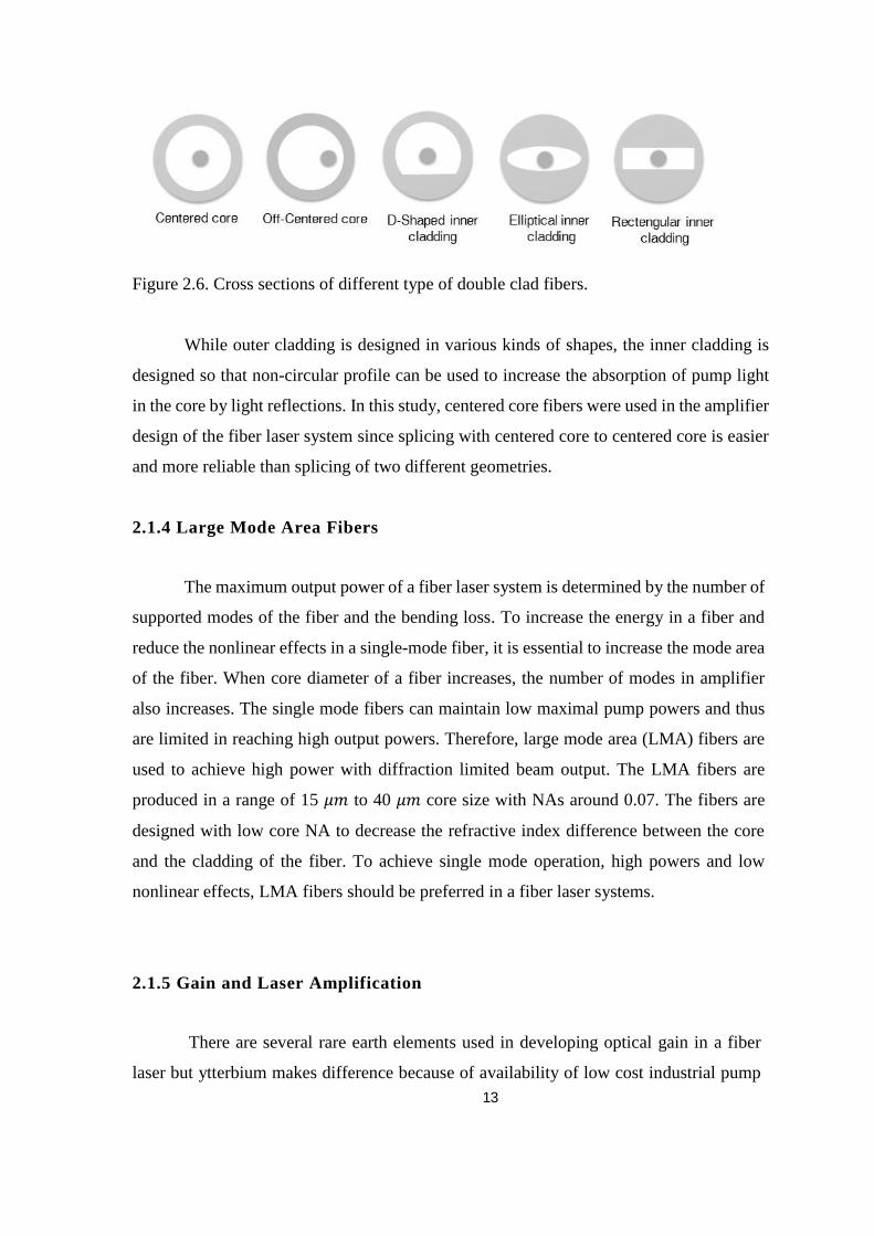
Figure 2.6. Cross sections of different type of double clad fibers. ..................................... 13
Figure 2.7. Illustration of three and four level lasing .......................................................... 14
Figure 2.8. Energy levels for a two level system. ................................................................ 15
Figure 2.9. Schematic of a fiber MOPA system .................................................................. 22
Figure 3.10. A simple laser – material interaction model ................................................... 23
Figure 3.1 Laser light interactions with materials ............................................................... 25
Figure 3.2 The absorption of laser output at different wavelengths varies according to the
materials involved (adopted from [34]) ............................................................................... 28
Figure 3.3 Effects after interaction of lasers with material. Orange arrows indicate heat
conduction. ............................................................................................................................ 29
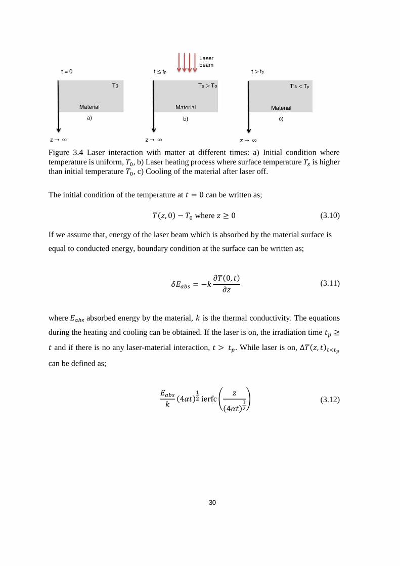
Figure 3.4 Laser interaction with matter at different times: a) Initial condition where
temperature is uniform, 𝑻𝟎 b) Laser heating process where surface temperature 𝑻𝒔 is higher
than initial temperature 𝑻𝟎, c) Cooling of the material after laser off. ............................... 30
Figure 3. 5 The melting depths for pulsed laser applications. a) At constant pulse widths b)
At constant power density (adopted from [36]) ................................................................... 32
Figure 3.6 The laser induced breakdown mechanisms : ionization by a) avalanche
breakdown b) multiphoton absorption ................................................................................. 34
Figure 3.7 Different laser pulse shapes; a) rectangular, b) smooth, c) triangular, d) random
shapes. .................................................................................................................................... 36

xv
Figure 3. 8 Scheme of temperature difference on material surface during pulsed operation
a) single pulse, b) multipulse laser operation on material. .................................................. 37
Figure 3.9 The basic configuration of material processing with scanhead ........................ 38
Figure 4.1 The configuration of the diode modulation system. .......................................... 42
Figure 4.2 Pulse shape of the modulated seed signal .......................................................... 44
Figure 4.3 Optical pulse shape generated by electrical pulse (inset: pulse train for 100 kHz
repetition rate) ....................................................................................................................... 44
Figure 4.4 The first amplification part of the preamplifier stage. WDM : wavelength
division multiplexer, PLP : pump laser protector ................................................................ 46
Figure 4.5 Spectrum of the seed diode ................................................................................ 47
Figure 4.6 Numerical simulation results for a) pump power, b) signal power, c) ASE power
as a function of fiber length for pump power of 100 mW, 200 mW and 300 mW. .......... 48
Figure 4.7 Pump power vs. output power from ytterbium doped fiber output. ................. 49
Figure 4.8 Spectrum of the a) ytterbium doped fiber output (logarithmic scale) .............. 50
Figure 4.9 The preamplifier system ..................................................................................... 50
Figure 4.10 Numerical simulation results for a) pump power, b) signal power, c) ASE
power as a function of fiber length for pump power of 100 mW, 200 mW and 300 mW for
the 2nd stage of the preamplifier. ......................................................................................... 51
Figure 4.11 The output power of the Yb doped fiber as a function of the pump power ... 52
Figure 4.12 Spectrum of ytterbium output (logarithmic scale), inset : linear scale. .......... 52
Figure 4.13 The spectrum of the preamplifier stage (logarithmic scale), inset : linear scale.
............................................................................................................................................... 53
Figure 4.14 Simple schematic of the middle amplifier stage. CPS : Cladding pump stripper,
MPC: multi pump combiner. ............................................................................................... 54
Figure 4.15 Simulation results for determining length of the fiber at 976 nm pump power
............................................................................................................................................... 55
Figure 4.16 Simulation results for a)972 nm pump wavelength b) 980 nm pump
wavelength. ........................................................................................................................... 56
Figure 4.17 Measured signal power as a function of pump power. ................................... 56
Figure 4.18 Design of the CPS ............................................................................................. 57

xvi
Figure 4.19 The spectrum of the ytterbium fiber output, inset : CPS output. .................... 58
Figure 4.20 Simple schematic of the main amplifier of the system.................................... 59
Figure 4.21 a) Simple schematic of the fiber splice, b) splice image of middle amplifier
output fiber to MPC input fiber of the amplifier. ................................................................. 60
Figure 4.22 Measured maximum emission wavelengths of the diodes as a function of
applied current at room temperature. ................................................................................... 61
Figure 4.23 Simulation results for amplifier stage at different pump wavelengths at a) 970
nm b) 973 nm c) 976 nm d) 979 nm ..................................................................................... 62
Figure 4.24 Splice image of MPC output fiber with ytterbium doped fiber. ..................... 63
Figure 4.25 Residual pump at ytterbium fiber output as a function of pump power. ........ 64
Figure 4.26 Measured signal power as a function of pump power at CPS fiber output. ... 65
Figure 4.27 Measured power as a function of pump power at the output of the collimated
isolator.................................................................................................................................... 66
Figure 4.28 Pulse shapes at different output powers at 100 kHz repetition rate ............... 68
Figure 4.29 Pulse shapes and durations at different repetition rates at constant (60W)
average power........................................................................................................................ 68
Figure 4.30 The optical spectra of the output signal for 20,30,40,50,60W powers. (inset :
logarithmic scale). ................................................................................................................. 70
Figure 4.31 Spectrum of the signal at 60 W with different repetition rates. (logarithmic
scale). ..................................................................................................................................... 70
Figure 4.32 The beam quality factor as a function of coiling radius of ytterbium doped fiber.
................................................................................................................................................ 72
Figure 4.33 Beam quality factor measurement at maximum operating power. ................. 72
Figure 4.34 Beam profile of the laser output a) 2D profile, b) 3D profile ......................... 73
Figure 4.35 Output power fluctuations measured at 10 s intervals. .................................... 74
Figure 4.36 Photo of the experimental setup ....................................................................... 75
Figure 4.37 Simple schematic of the signal modulation mechanism in electronic card. ... 76
Figure 4.38 Industrialized design of the preamplifier stage. ............................................... 77
Figure 4.39 A simple schematic of industrial system. ......................................................... 78
Figure 4.40 The industrialized laser amplifier. .................................................................... 79

xvii
Figure 4.41 Laser system with galvanometric scanner. ...................................................... 80
Figure 5.1 The demonstration of the pulse overlapping. .................................................... 84
Figure 5.2 Percentage of pulse overlap as a function of repetition rate in different scan
speeds. ................................................................................................................................... 85
Figure 5.3 Pulse to pulse formation at 100 kHz repetition rate on the material with scanning
speed a)3800 mm/s b) 2200 mm/s. ...................................................................................... 86
Figure 5. 4 Schematic diagram of microdrilling experimental setup. ................................ 87
Figure 5.5 Microdrilling time with respect to average power and pulse duration for a) steel
b) Al. ...................................................................................................................................... 88
Figure 5.6 SEM images of microdrilling applications on stainless steel and aluminium with
15 W average power and 203, 305 and 407 ns pulse duration ........................................... 90
Figure 5.7 SEM images of microdrilling attempts on 0.1 mm stainless steel in same
exposure time 8 ms at 20 W average power and different pulse durations a) 100 ns b) 200
ns c) 300 ns d) 400 ns. .......................................................................................................... 91
Figure 5.8 SEM image of laser processing on silicon with scan speed 2500 mm/s and
different average power. Laser power at 60 W, 50 W and 40 W from left to right. ......... 93
Figure 5.9 Laser edge isolation process on textured Si cell by same average power and
scan speed but different laser beam spot sizes by a) 100 mm b) 160 mm focal length
objectives. .............................................................................................................................. 94
Figure 5.10 Processing of silicon wafer with different pulse overlapping a) 2000 mm/s b)
1500 mm/s c) 500 mm/s scan seeds at 100 kHz repetition rate. ......................................... 95
Figure 5.11 Top view of the processed full scale silicon wafer with 1500 mm/s scan speed
and 60 W average power ...................................................................................................... 96
Figure 5.12 Schematics of inference based color marking mechanism ......................... .97
Figure 5.13 Effect of scan speed on color marking of stainless steel. ................................ 98
Figure 5.14 Marking stainless steel with constant peak power varied average power and
pulse duration. ....................................................................................................................... 99
Figure 5.15 Marking stainless steel with constant peak and average power ................... 100
Figure 5.16 Marking stainless steel with varied peak power and constant pulse energy.100
Figure 5.17 Color marking samples. .................................................................................. 101

xviii
Figure 5.18 The depth of engraving as a function of scan number at different repetition rates
(100,120,140,160 kHz) with 1000 mm/s scan speed. ....................................................... 103
Figure 5.19 The engraved Al sample with different scan cycle a) 20 b) 40 c) 60 d) 80 e)100
f) 120 g) 140 times. ............................................................................................................. 104
Figure 5.20 The depth of engraving as a function of scan number at 100 kHz repetition rate
and 500 mm/s scan speed. .................................................................................................. 105
Figure 5.21 Some of the engraving and cutting samples prepared by laser amplifier;
engraving of a) 14 carat gold, b) stainless steel, d) brass, cutting of c-d) aluminum. ...... 106
Figure 5.22 Application samples done by developed fiber laser amplifier : marking of a
stainless steel a), plastics b) and c), brass d), denim e), stainless steel f), leather g), cart i);
day&night marking of aluminium h); precise cutting of a stainless steel k);
micromachining of titanium j) ; dye removal of aluminium l); microdrilling of silver m);
sintering n); label marking o). ............................................................................................. 107

1
CHAPTER 1
INTRODUCTION
1.1 Brief History and Evolution of Fiber Lasers and Amplifiers
The idea of generating fiber lasers and amplifiers began with the development of fiber
optical communication technology. The first fibers which were based on total internal
reflection principle [1], were uncladded and so, guiding of light was a problem. After
development of the silica cladded fibers in 1950s [2; 3], progress of fiber laser technology
accelerated because guiding of light was improved by clads. The cladded fibers enhanced fiber
performance and changed the perspective of scientists to fiber optics technology. The first fiber
laser cavity was built in 1961 by using a neodymium 3+ doped fiber [4]. Then, the reduction
in required pump power for a laser gain in lasers and amplifiers was first demonstrated in
1960s [5; 6] in which both signal and pump propagated in a small diameter fiber core.
However, scientists used a lamp source to pump the laser medium in fibers so it took more
than ten years for diode pumps to reach maturity. The development of first ytterbium fiber
laser in 1962 [7] showed that ytterbium was less attractive than neodymium as an active
ion and thus conversion efficiencies and high output powers became crucial. Fibers with
losses less than 20 dB/km were developed and this made them convenient for telecom
applications in 1970 [8]. The development of first room temperature operation Nd-doped
fiber lasers also made a contribution to progress of fiber lasers and amplifiers in 1970s
[9]. Despite progress on different doped type of fibers, laser systems were operating with
low conversion efficiency. The progress of fiber clad technology went on by trying
different dopants and dopant concentrations to reach high conversion efficiency. After the
evolution of diode pumps and developing techniques for producing low insertion loss rare-
earth metal doped fibers for 1550 nm wavelength in the late 1970s [10] and with the
emergence of optical communications, first erbium doped fiber amplifier was
demonstrated in 1987 [11]. In terms of average power, the basic problem was low
conversion efficiency of erbium due to limitation of doping concentration of erbium
fibers, so development of ytterbium and neodymium doped fibers became crucial for high

2
average power outputs. The first fiber laser amplifiers, where the pump and signal
propagated in a small core, were hard to couple a high power signal and pump light into
the core. In addition, single mode diodes which are power limited and expensive need to
be used to achieve core pumping method. The cladding pumping technique was developed
in order to solve this problem in 1988 [12], which was another significant step forward in
the evolution of high average powers of fiber lasers. If the geometry of fiber clad and core
are appropriate, doped core can absorb pump more effectively and high optical gain can
be produced by active ions in the core. The absorption of pump light of a rare-earth metal
double clad was improved by modelling different fiber designs such as D-shaped and
rectangular core typed fibers.
The development of cladding pumping technique lead to increase in the average
powers gradually since the mid-1990s. After recognition of the potential of ytterbium
doped fiber lasers, the first watt-level ytterbium fiber laser was built in 1995 [13]. The
deep understanding of thermo optical properties of doped fibers evoked 35 watts single
mode ytterbium doped double clad configuration continuous (CW) fiber laser
development in 1997 [14]. The first fiber laser above 100 watt average power was built in
1999 with 58% optical to optical conversion efficiency. [15]. Then, the first kW regime
fiber laser was reported in 2002 [16] by developing 1 kW ytterbium doped fiber laser with
80% conversion efficiency at the 1.09 m wavelength. 1.36 kW and nearly diffraction
limited fiber laser system was constructed with 83% slope efficiency at 1.1 um wavelength
regime in 2004 [17]. The first commercial 10 kW fiber laser, which was planned to weld
metal parts, was reported in 2010 [18]. In addition, average power rate and peak power of
pulsed fiber laser systems increased at a similar rate. Ultrashort pulsed fiber laser systems
which have almost kW peak power can be built with today’s technology [19], while the
average power range used to be about 100 W in 2005 [20]. 2.2 mJ pulse energy has been
achieved in 2011 with 3.8 GW peak power by a fiber chirped amplification system which
has sub 500 fs pulses [21]. The rapid development was also seen in nanosecond pulsed
fiber laser amplifiers. The kW peak power level nanosecond pulsed fiber laser system,
which has 49% optical to optical efficiency, was developed in 2009 [22]. The high pulse
energy generating techniques were also developed and 11 mJ fiber master oscillator
amplifier was built in 2013 with 660 ns pulse duration [23]. The evolution of the average
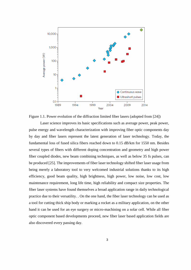
power of continuous and ultrashort pulsed fiber laser systems are shown in Figure 1.1.
3
Figure 1.1. Power evolution of the diffraction limited fiber lasers (adopted from [24])
Laser science improves its basic specifications such as average power, peak power,
pulse energy and wavelength characterization with improving fiber optic components day
by day and fiber lasers represent the latest generation of laser technology. Today, the
fundamental loss of fused silica fibers reached down to 0.15 dB/km for 1550 nm. Besides
several types of fibers with different doping concentration and geometry and high power
fiber coupled diodes, new beam combining techniques, as well as below 35 fs pulses, can
be produced [25]. The improvements of fiber laser technology shifted fiber laser usage from
being merely a laboratory tool to very welcomed industrial solutions thanks to its high
efficiency, good beam quality, high brightness, high power, low noise, low cost, low
maintenance requirement, long life time, high reliability and compact size properties. The
fiber laser systems have found themselves a broad application range in daily technological
practice due to their versatility. . On the one hand, the fiber laser technology can be used as
a tool for cutting thick ship body or marking a rocket as a military application, on the other
hand it can be used for an eye surgery or micro-machining on a solar cell. While all fiber
optic component based developments proceed, new fiber laser based application fields are
also discovered every passing day.

4
There are several techniques used to build a fiber laser amplifier depending on the
application but the core technology mainly depends on master oscillator power amplifier
design.
1.2 Laser Material Processing
The laser material interaction is one of the ever-growing field of science for years and
its progress is parallel to emerging designs of new laser systems. Material processing with
lasers has several advantages as compared to traditional methods. Material processing
applications with lasers are used since 1960s [26] and demand grows day by day. After
invention of new laser types and development in applied sciences and industry in the world,
processing of materials with lasers became increasingly important.
Using a laser as a material processor have several advantages. One of the main
advantages is the ability to control laser beam and laser energy on the material with high
precision. The second main advantage is that the processing techniques with laser are very cost
effective since laser processing is non-contact and eliminates tool wearing. Third, it is a
chemical free application, that is, it is a clean technique for processing applications. Fourth, it
is possible to remove material by adjusting the wavelength or intensity, selective material
removal is possible without damaging the under layer. The evolution of the laser material
processing accelerated with increasing laser output power levels. The first studies for laser
processing applications was made by ruby laser after realizing that it can be used as a good
pulsed laser drilling tool. The first attempts to use lasers for material processing took place in
mid-1960s. The first pulsed ruby laser for welding applications was demonstrated by Platte and
Smith in 1963 to weld a stainless steel foil. Then the first scientific test drilling applications
were used for Gillette company to drill razor blades [27]. The first ruby laser was used as an
industrial tool by Western Electric to drill wire drawing die in 1965 [28]. After discovering the
ability of CO₂ lasers as a cutting tool, 1 mm thick steel was cut by the first oxygen assisted 300
W CO₂ laser. Later, CO₂ lasers were commercially used for scribing ceramics by Western
Electric in 1967 [27]. The lasers were considered as a material process tool rather than a simple
light source in 1970s. The new techniques and new laser types were developed for industrial
applications such as cutting, marking, drilling and welding as the first successful industrialized
lasers were produced. The usage of lasers in heat treatment, alloying, glazing and as a thin film

5
deposition tool started in the early 1980s and accelerated in early 1990s. The studies on high
precision material processing has accelerated with development of the high power fiber lasers
as an industrial product in the early 1990s. By the invention of fiber lasers, fast, efficient and
precise material processing period started.
The material processing with laser is a unique way for a wide range of materials
such as metals, ceramics, alloys, polymers, composites and glasses and the laser radiation
can be generated as pulsed or continuous wave at various wavelengths, at power levels
ranging miliwatts to kilowatts. Processing matter in macroscopic and microscopic scales is
also possible by using different properties of laser. There are several types of lasers to
perform material processing tasks, which can be listed as marking, cutting, surface
treatment, coding, engraving, welding, drilling, rapid prototyping and others. The typical
lasers for materials processing are Nd-YAG, CO₂, fiber lasers, excimer lasers, atomic gas
lasers, ion lasers, and molecular gas lasers.

6
7
CHAPTER 2
THE OPERATION PRINCIPLES OF FIBER LASER COMPONENTS
2.1 Theory of Fiber Lasers and Amplifiers
In this section, theory of the fiber lasers and amplifiers will be discussed in
relationship with the components constituting the fiber laser amplifiers.
2.1.1 Optical Fibers
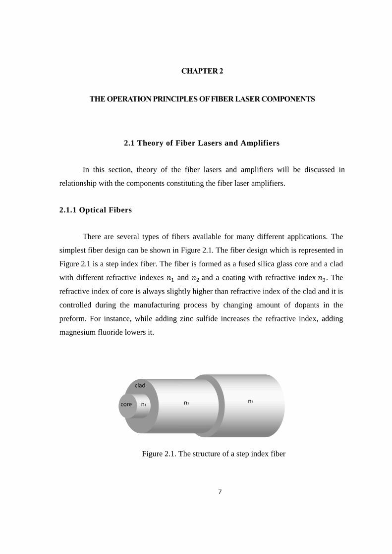
There are several types of fibers available for many different applications. The
simplest fiber design can be shown in Figure 2.1. The fiber design which is represented in
Figure 2.1 is a step index fiber. The fiber is formed as a fused silica glass core and a clad
with different refractive indexes 𝑛1 and 𝑛2 and a coating with refractive index 𝑛3. The
refractive index of core is always slightly higher than refractive index of the clad and it is
controlled during the manufacturing process by changing amount of dopants in the
preform. For instance, while adding zinc sulfide increases the refractive index, adding
magnesium fluoride lowers it.
Figure 2.1. The structure of a step index fiber

8
The guiding of the light occurs inside the fiber by the help of the clad and the
guiding is based on the total internal reflection principle (Figure 2.2). The light propagate
inside the core and some part of it penetrates into the cladding of the fiber. The protective
coating (primary buffer) of the fiber is used to protect glass surface of clad from the
external damage and strip away unwanted light inside the fiber and it reduces the internal
reflection at the cladding.
Figure 2.2. The propagation of light inside the fiber
The total internal reflection principle works by the help of index differences of the
core and clad of the fiber. The index differences of the core and clad determine the
numerical aperture (NA) of the fiber which is a parameter defining how much light can
be collected by the fiber (Figure 2.3).
Figure 2.3. Light Propagation for calculating total internal reflection
In fiber end face, critical angle can be calculated by using Snell’s law;
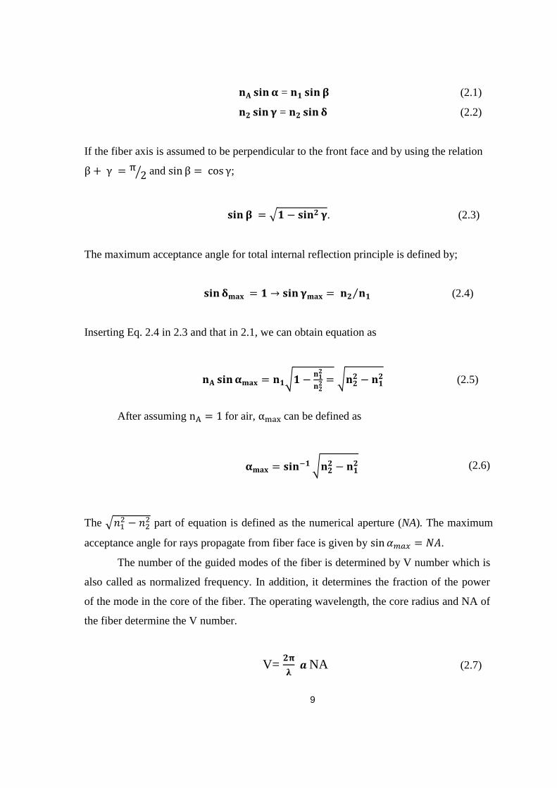
9
𝐧𝐀 𝐬𝐢𝐧 𝛂 = 𝐧𝟏 𝐬𝐢𝐧 𝛃 (2.1)
𝐧𝟐 𝐬𝐢𝐧 𝛄 = 𝐧𝟐 𝐬𝐢𝐧 𝛅 (2.2)
If the fiber axis is assumed to be perpendicular to the front face and by using the relation
β + γ = π2⁄ and sin β = cos γ;
𝐬𝐢𝐧 𝛃 = √𝟏 − 𝐬𝐢𝐧𝟐 𝛄. (2.3)
The maximum acceptance angle for total internal reflection principle is defined by;
𝐬𝐢𝐧 𝛅𝐦𝐚𝐱 = 𝟏 → 𝐬𝐢𝐧 𝛄𝐦𝐚𝐱 = 𝐧𝟐 𝐧𝟏⁄ (2.4)
Inserting Eq. 2.4 in 2.3 and that in 2.1, we can obtain equation as
𝐧𝐀 𝐬𝐢𝐧𝛂𝐦𝐚𝐱 = 𝐧𝟏√𝟏 −𝐧𝟏
𝟐
𝐧𝟐𝟐 = √𝐧𝟐
𝟐 − 𝐧𝟏𝟐 (2.5)
After assuming nA = 1 for air, αmax can be defined as
𝛂𝐦𝐚𝐱 = 𝐬𝐢𝐧−𝟏 √𝐧𝟐𝟐 − 𝐧𝟏
𝟐 (2.6)
The √𝑛12 − 𝑛2
2 part of equation is defined as the numerical aperture (NA). The maximum
acceptance angle for rays propagate from fiber face is given by sin 𝛼𝑚𝑎𝑥 = 𝑁𝐴.
The number of the guided modes of the fiber is determined by V number which is
also called as normalized frequency. In addition, it determines the fraction of the power
of the mode in the core of the fiber. The operating wavelength, the core radius and NA of
the fiber determine the V number.
V= 𝟐𝛑
𝛌 𝒂 NA (2.7)

10
𝑎 is radius of the fiber core and 𝜆 is wavelength of the light. If the V number is smaller
than 2.405, a single mode propagation is obtained in fiber. The single mode fiber allows
to transmit only fundamental mode of light. A multi-mode propagation is seen, if the V
number is higher than 2.405. For multi-mode fibers, loss of propagation in the core is
higher than single-mode fibers due the high numerical aperture. They allow guiding of
different wavelengths of light. Multi-mode fibers have much higher V numbers and the
number of supported modes for a multi-mode step index fiber can be approximated as;
M ≈ 𝟒
𝛑𝐕𝟐 (2.8)
2.1.2 Ytterbium Doped Silica Fibers
Ytterbium is a rare-earth metal and has a number of interesting properties for the
fiber laser amplifiers especially for high power applications. Using a rare-earth metal
doped fiber in a fiber laser amplifier provides low noise, high power output, broad gain
bandwidth, high beam quality, tunability, narrow linewidth and low cost design.
Absorption and emission cross section of ytterbium are very broad and absorption spectra
allows wide range of wavelength to pump. It has a very simple electronic structure with a
ground state manifold ²𝐹7/2 with three Stark sub-levels and an excited manifold ²𝐹5/2 with
four Stark sub-levels. The energy gap between the ground and the exited state is large
(Figure 2.4) and this situation prevents nonradiative decay by way of multiphoton emission
from exited manifold even in a small sized high energy silica material, hence the fibers
doped with ytterbium element allows very high power efficiencies of fiber laser
amplifiers. They also have lower thermal effects than other laser gain medias due to small
quantum defect of ytterbium element, so the heating effect of such media is three times
smaller than Nd-YAG [13]. Moreover, the ytterbium doped gain media has a longer
relaxation time than other types of media, thus lower threshold pump power may be
adequate for signal gain.

11
Figure 2.4. Energy level structure of ytterbium ion.
The emission spectra of ytterbium doped fibers depends on composition of host
glass [27]. The emission and absorption cross-sections of ytterbium doped
germanosilicate glass are shown in the Figure 2.5 and cross-sections can vary depending
on the content of host glass composition. The local maxima of cross-sections of ytterbium
is at 975 nm and 910 nm. The first absorption peak of the ytterbium ion is 975 nm which
represents zero-line transition between the lowest levels of higher state and lower state.
The laser dynamics at 975 nm wavelength is three level since the emission is based upon
a transition to the lowest Stark level. The other peak at 910 nm has broad cross-section
where high power pumping is required to get high gain since the absorption is three times
lower than 975 nm cross-section. Hence, while pumping at 910 nm, longer fiber should
be used to achieve same output power as in the case of 975 nm.
While the lifetime of the Yb+3 in excited state for a pure silicate glass is 1.5 ms, it
is 0.8 ms for a germanosilicate glass since higher germanium content in the core tends
shorten lifetimes. The situation affects the performance of a master oscillator power
amplifier (MOPA) system which typically operates at kHz levels since lower repetition
rate means higher spontaneous emission.

12
Figure 2.5. Emission and absorption cross-sections of ytterbium doped germanosilicate
glass as used in the cores of ytterbium doped fiber.
2.1.3 Double-Clad Fibers
After the development of the double-clad fibers, achieving high power output by
a fiber laser amplifier became possible since pumping a single clad fiber with high pump
levels is extremely difficult. The powers for pumping a single mode fiber are limited
below 1 W. The development of the fiber coupled multimode diodes lead to reach more
than 100 W pump power by a single emitter. The cladding pumping technique with double
clad fibers became essential to transfer high pump power into the small core of the fiber.
The design of a double clad fiber can be seen in Figure 2.6 where the outer cladding with
lower refractive index than inner cladding and core. The low numerical aperture of core
leads to a single mode propagation inside the core and the high numerical aperture and
greater than hundred micrometers of inner clad supports in a large number of modes. To
increase the pump absorption in a double clad fiber, different fiber geometries such as
offset-core, octagonal, D-shaped and square can be used.
13
Figure 2.6. Cross sections of different type of double clad fibers.
While outer cladding is designed in various kinds of shapes, the inner cladding is
designed so that non-circular profile can be used to increase the absorption of pump light
in the core by light reflections. In this study, centered core fibers were used in the amplifier
design of the fiber laser system since splicing with centered core to centered core is easier
and more reliable than splicing of two different geometries.
2.1.4 Large Mode Area Fibers
The maximum output power of a fiber laser system is determined by the number of
supported modes of the fiber and the bending loss. To increase the energy in a fiber and
reduce the nonlinear effects in a single-mode fiber, it is essential to increase the mode area
of the fiber. When core diameter of a fiber increases, the number of modes in amplifier
also increases. The single mode fibers can maintain low maximal pump powers and thus
are limited in reaching high output powers. Therefore, large mode area (LMA) fibers are
used to achieve high power with diffraction limited beam output. The LMA fibers are
produced in a range of 15 𝜇𝑚 to 40 𝜇𝑚 core size with NAs around 0.07. The fibers are
designed with low core NA to decrease the refractive index difference between the core
and the cladding of the fiber. To achieve single mode operation, high powers and low
nonlinear effects, LMA fibers should be preferred in a fiber laser systems.
2.1.5 Gain and Laser Amplification
There are several rare earth elements used in developing optical gain in a fiber
laser but ytterbium makes difference because of availability of low cost industrial pump

14
sources and emission spectrum. The gain dynamics of the rare earth element doped fibers
is similar although they have different emission and absorption spectra and applications.
The gain dynamics can be categorized into three groups, such as two level, three level and
four level systems. The two level laser medium cannot be used for light amplification
since probability of pumping the ions into higher energy state is equal the probability of
stimulating them back down. The three and four level system are illustrated in Figure 2.7.
Figure 2.7. Illustration of three and four level lasing
In both three and four level lasing, rare earth ions are excited to higher energy
levels via the absorption of high energy pump photons. This process is known as
“pumping”. The higher state is a short-lived state, so ions rapidly decay to lower energy
state which is also called a metastable state, without radiation just after the pumping
process. The energy which is achieved in higher energy levels is used to amplify signal
by stimulated emission. The amplification achieved via transfer from pump to signal. The
difference between three and four level system is in type of the final energy state of ions
after the stimulated emission process. The process ends up in the ground state for a three-
level system, while it ends up at an excited state in a four-level system. Higher population
density in the upper energy level is required for both of the systems, accordingly so high
pump power is a necessity.

15
In this study, ytterbium doped gain media is used to amplify signals where
ytterbium has a three level lasing scheme. Rate equations are very important to understand
the amplification behavior of this type of systems. Ytterbium based fiber laser amplifier
theory was first discussed for rare-earth metal doped fiber lasers for a shorter emission
wavelength in 1994 [28]. In this thesis, a ytterbium doped media will be discussed and it
can be modeled by pump excitation and de-excitation rates and seed absorption and
emission rates. A two-level laser scheme can be used to model 976 nm ytterbium fiber
laser pumping. The Figure 2.8 shows an energy diagram of a two level system where
excitation and de-excitation rates of pump are indicated as 𝑅12 and 𝑅21 respectively,
signal absorption and emission rates are 𝑊12 and 𝑊21respectively. 𝐴21 is the spontaneous
emission rate.
Figure 2.8. Energy levels for a two level system.
The rate equations can be written by indicating population densities as 𝑁1, 𝑁2 for
lower and upper state respectively.
𝒅𝑵𝟐
𝒅𝒕= (𝐖𝟏𝟐 + 𝐑𝟏𝟐 )𝐍𝟏 − (𝐖𝟐𝟏 + 𝐑𝟐𝟏)𝐍𝟐 − 𝐀𝟐𝟏𝐍𝟐 (2.9)
𝑑𝑁1
𝑑𝑡= −(𝑊12 + 𝑅12 )𝑁1 + (𝑊21 + 𝑅21)𝑁2 + 𝐴21𝑁2 (2.10)

16
Where 𝑁1 + 𝑁2 = 1 by the energy conservation law and 𝑑𝑁𝑖 𝑑𝑡⁄ = 0 for steady state
conditions so;
𝑁1 =𝑊21 + 𝑅21 + 𝐴21
𝑊21 + 𝑊12 + 𝑅21 + 𝑅12 + 𝐴21 (2.11)
𝑁2 =𝑊12 + 𝑅12
𝑊21 + 𝑊12 + 𝑅21 + 𝑅12 + 𝐴21 (2.12)
where the spontaneous emission rate is depend on the life time of the Yb ions ( 𝜏 ) in upper
level and can be shown;
𝐴21 =1
𝜏 (2.13)
The absorption and emission cross section of Yb ion in the fiber core determine the
signal and pump transition rates of system and can be defined as;
𝑊12 =𝜎𝑎𝑠𝐼𝑠ℎ𝑣𝑠
, 𝑊21 =𝜎𝑒𝑠𝐼𝑠ℎ𝑣𝑠
, (2.14)
𝑅12 =𝜎𝑎𝑝𝐼𝑝
ℎ𝑣𝑝, 𝑅21 =
𝜎𝑒𝑝𝐼𝑝
ℎ𝑣𝑝, (2.15)
where 𝐼𝑠 and 𝐼𝑝 are corresponding intensities for signal and pump respectively with
transition frequencies of signal 𝑣𝑠 and transition frequency of pump ℎ𝑣𝑝. 𝜎𝑎𝑠 and 𝜎𝑎𝑝 are
the absorption of signal and pump cross sections respectively. 𝜎𝑒𝑠 and 𝜎𝑒𝑝 are the emission
of signal and pump cross sections respectively. The pump and signal power variations can
be expressed for a two level system. The propagation equation of the pump and signal along
the fiber is defined in equations Eq. 2.16 and Eq. 2.17 respectively;
17
𝑑𝑃𝑝
𝑑𝑧= 𝐼𝑝𝑁𝑡(𝜎𝑒𝑝𝑁2 − 𝜎𝑎𝑝𝑁1)𝑃𝑝(𝑧) (2.16)
𝑑𝑃𝑠
𝑑𝑧= 𝐼𝑠𝑁𝑡(𝜎𝑒𝑠𝑁2 − 𝜎𝑎𝑠𝑁1)𝑃𝑠(𝑧)
(2.17)
In the equations above, 𝑁𝑡 is the ion density and ⌈𝑝 and ⌈𝑠 are pump overlap factor and the
signal overlap factor respectively. ⌈𝑝 can be defined as equation
𝑆𝑝𝑐
𝑆𝑑 (2.18)
where 𝑆𝑝𝑐 is area of the pumping core and 𝑆𝑑 is doped area of the gain and ⌈𝑠 is the overlap
of mode field with doped media. The small gain coefficient 𝑔(𝑧) can be defined by using
propagation of seed equation as;
𝑔(𝑧) = 𝐼𝑠𝑁𝑡(𝜎𝑒𝑠𝑁2 − 𝜎𝑎𝑠𝑁1) (2.19)
2.1.6 Limitations of the amplifier
To develop a reliable and durable fiber laser amplifier, many physical limitations
should be eliminated and experimental outputs should be monitored accurately. Since the
light propagates in a very small mode size and long nonlinear medium, encountering
nonlinear effects is inevitable in a fiber laser amplifier. Moreover, damage thresholds of
the components and thermal limitations, splice losses and photodarkening are the other
main factors which affect the performance of the amplifier. In this section, the limitations
which affects reaching high pulse energy and power in a nanosecond pulsed fiber laser
amplifier will be explained.
The power density of electromagnetic field is very high in an optical fiber since
the laser signal propagates in the order of micron size. Moreover, the cavity length of a
laser system can be very long, thus the fibers exhibit a variety of nonlinear effects. The
18
nonlinear effects such as stimulated Raman scattering, stimulated Brilluion scattering and
the Kerr effect play an important role in the performance of a high power fiber laser
system, especially during high power and high pulse energy operation.
The interaction of light with acoustic phonons, which results in a frequency
shift, lead to stimulated Brillouin scattering (SBS) in narrow linewidth fiber laser
amplifiers. SBS can be observed even in very low power levels [29]. The scattered
photons propagate in the opposite direction of the pump photons by the reason of
conservation of momentum principle. If a narrow pulse is used in an fiber optical system
and annihilation of signal is neglected, the threshold of SBS can be expressed as,
𝑃𝐶𝑅 = 21𝐴𝑒𝑓𝑓
𝑔𝐵𝐿𝑒𝑓𝑓
(2.20)
where 𝑔𝐵 is the Brillouin factor and it is equal to 5 × 10⁻¹¹ m/W for a typical doped silica
fiber [30], 𝑃𝐶𝑅 is the critical power where Brillouin scattering occurs, 𝐴𝑒𝑓𝑓 is the effective
mode area of the fiber, 𝐿𝑒𝑓𝑓 is the effective fiber length. The effective fiber length depends
on attenuation coefficient of the fiber 𝛼𝑝 and can be expressed as
𝐿𝑒𝑓𝑓 =
1
𝛼𝑝[1 − 𝑒−(𝛼𝑝𝐿)].
(2.21)
Stimulated Raman scattering (SRS) is an inelastic scattering and it is observed due
to scattering of photons by optical phonons. In SRS process, forward and backward
scattering can be observed and it limits the average power of pulsed fiber laser systems.
It is observed in fiber laser amplifiers while pumping a gain to amplify signal. The peak
of the Raman gain is 1 × 10⁻¹³ m/W for 1 𝜇𝑚 wavelength. The same approach with
equation 2.20 can be used to calculate threshold power for SRS,
𝑃𝐶𝑅 = 16𝐴𝑒𝑓𝑓
𝑔𝑅𝐿𝑒𝑓𝑓 (2.22)

19
where 𝑔𝑅is the Raman factor and equal to 3.2 × 10⁻¹³ m/W for silica [29].
Four-wave mixing (FWM) is another nonlinear effect which occurs when at least
two different wavelengths propagate in an optical fiber. In a fiber laser amplifier, FWM
can be defined as noise generation by energy transfer of pump to signal. FWM increases
the noise of the amplifier and affects the performance of fiber laser amplifiers. If we
assume that at least two incident different wavelength 𝑣1 and 𝑣2 where 𝑣2 > 𝑣1 propagate
in an optical fiber, they interact with each other and create two new wavelengths 𝑣3 and
𝑣4 at different frequency by the following equations.
𝑣3 = 𝑣1 − (𝑣2 − 𝑣1), (2.23)
𝑣4 = 𝑣2 + (𝑣2 − 𝑣1).
(2.24)
The refractive index in a non-linear optical medium, depends on the optical
intensity and, can change at higher intensities. The change in refractive index of a material
is referred as Kerr effect. Self-phase modulation (SPM) and cross-phase modulation are
refractive index changes due to nonlinear effects. SPM occurs at high optical intensities
and can be described by
𝑛′ = 𝑛 + 𝑛2𝐼, (2.25)
where 𝑛2 is the nonlinear index coefficient and 𝐼 is the intensity inside the fiber. In this
equation, 𝑛′ − 𝑛 is nonlinear change in the refractive index. In SPM, when the refractive
index of the medium increases, a phase shift in the pulse is observed. Cross-phase
modulation (XPM) effect is also an optical phase shift in a light beam as SPM, however
it is induced by changing a phase of a wavelength by another wavelength. SMP and XPM
can be suppressed in a fiber laser amplifier by increasing the mode field diameter of the
fiber.
Photodarkening is a transmission loss effect in the gain medium of amplifier in
fiber lasers and it affects the long term reliability of system. In a doped media, the
reversible absorption centers can be created in time via irradiation of light at a certain

20
wavelengths, hence transmission losses of the doped medium may increase. The higher
doping concentration causes more reversible absorption centers, so choosing low doping
concentration fibers is a solution to eliminate photodarkening affect.
Efficient light confinement in the core of a double clad fiber is another important
factor in high power fiber lasers in constructing a good fiber amplifier, hence a good
cladding strip operation is necessary to protect coating of the fiber. If residual pump light
propagates in a double clad fiber, it can damage coating of the fiber or laser components
even at low powers in time. The cladding pump can be eliminated from the fiber by using
cladding pump strippers. The thermal effects on the fiber coating should be managed in
order to maintain a long term high power output from the amplifier.
2.1.7 Amplified Spontaneous Emission
The physical and quantitative understandings of noise (or parasitic background) in
an optically amplified system play an important role to optimize the fiber devices.
Amplified spontaneous emission (ASE) is a type of noise that is caused by spontaneous
de-excitation in an active media. After population inversion process, the excited ions
without any coherence property can be generated while they turn back to the ground state
without stimulation. The generated spontaneous emission gets amplified in forward and
backward direction while it travels through the gain medium. All optical energy is
consumed into ASE while pumping a system, if there is no input signal. ASE can reach
high power level and saturate the gain of laser. There are several parameters that effect
the ASE rate in a fiber amplifier system, such as doping concentration of gain media and
length, signal and pump power, pump wavelength and repetition rate. ASE is one of the
most dominant noise in a tens of kHz repetition rate MOPA design fiber laser amplifier
that affects the performance of the system because ytterbium ion has 0.8-1 ms lifetime in
its excited state.
ASE can be modeled by using equation of the number of the randomly polarized
photons 𝑑𝑛(𝑣) between the ν and ν+δν frequencies as [31];

21
𝑑𝑛(𝑣) = 𝐴21𝑔(𝑣)𝛿(𝑣)∆Ω
4𝜋𝑑𝑉 ∫ 𝑁2(𝑟, 𝜃)
𝑠
𝜓𝑠(𝑟, 𝜃)𝑟 𝑑𝑟 𝑑𝜃 (2.26)
where 𝐴21 is the spontaneous decay rate which is equal to 1 𝜏⁄ . The lineshape function is
defined as 𝑔(𝑣), ∆Ω
4𝜋 is the spontaneous emission ration in the fiber and the volume
element 𝑑𝑉 =𝜋𝑤𝑠𝑑𝑧 . The overlap between the density distribution of excited ions and
guided mode expressed in the integral where 𝑁2 is the excited state populations, 𝜓𝑠(𝑟, 𝜃)
is the mode envelope and (𝑟, 𝜃) represents cylindrical transverse coordinates.
The spontaneous emission power per unit frequency can be found by 𝑑𝑃𝑆𝐸 =
ℎ𝑣𝑑𝑛(𝑣) and creation rate of the spontaneous emission power in bandwidth 𝛿𝑣 is;
𝑑𝑃𝑆𝐸
𝑑𝑧= 2𝑃0𝜎𝑒(𝑣)∫ 𝑁2(𝑟, 𝜃)
𝑠
𝜓𝑠(𝑟, 𝜃)𝑟 𝑑𝑟 𝑑𝜃 (2.27)
where the power of one spontaneous photon in a bandwidth of 𝛿𝑣 is 𝑃0.
2.1.8 Master Oscillator Power Amplifier (MOPA) Configuration
The master oscillator power amplifier is a type of fiber laser configuration where
the power amplifier is designed via fiber based components. In this design, there is a low
power laser seed which is increased to high power levels by rare-earth metal doped fibers
and high power pump diodes. MOPA configuration provides higher output power levels,
higher beam quality and higher efficiency than other type of bulk lasers. In a pulsed
MOPA system, pulse width of the seed is modulated externally and the doping gain is
pumped by a CW or pulsed pump source for achieving high power levels. The main
advantages of MOPA based fiber laser systems are independent and flexible control of
pulse width and repetition rate via external modulation. Moreover the systems can be
designed as pulse shape tunable and upgradable to higher output powers. Simple
schematic of a fiber MOPA system can be seen in Figure 2.9.

22
Figure 2.9. Schematic of a fiber MOPA system
The fiber MOPA system configuration can be as Figure 2.9 where fiber laser diode
is used as a master oscillator. Then an amplifier, which is pumped by a pump diode, is
constructed after oscillator stage to amplify seed laser. The seed signal and pump are
combined via a fiber coupler then ytterbium doped fiber is used to create a gain. The
amplification of the system can be raised by using another amplifier with ytterbium doped
fiber and pump diode, hence the MOPA system can be formed by using several amplifier
stages.
Despite the advantages of MOPA systems, their construction is more complicated
than Q-switched lasers which are the other most type of pulsed fiber lasers. However, Q-
switched fiber lasers are not flexible in their design. Moreover, changing of pulse duration
and repetition rate is not possible independent of each other in a Q-switched fiber laser.

23
CHAPTER 3
PHYSICAL MECHANISM BEHIND LASER MATERIAL PROCESSING
The effect of laser radiation effects on matter can be studied in several aspects such as,
electromagnetic, thermodynamic and optical interactions. After illuminating a material
with laser beam, the energy of the beam is transformed into electronic excitation energy.
After transforming process, by collisions between the lattice of material and that of
electrons, energy is transferred to the lattice. The energy of laser affects the material in
several ways such as ionization, temperature rise, vaporization and gasifying. The
interaction of laser and material can be described in a simple way by using heat flow
model which is represented in Figure 3.10. Here heat flow can be assumed to happen in z
axis and radius of the spot is larger than the penetration depth. The diameter of the
collimated beam is represented as D, focal length of the lens after focusing on a material
is f, the spot size is 2𝑤0.
Figure 3.10. A simple laser – material interaction model
24
There are several parameters which affect the processing of the material with lasers. First,
the material characteristic is important with specific property such as thermal diffusivity,
thermal conductivity, temperature and heat of vaporization. The reflectivity of the material
has a dependency on frequency of the laser radiation and temperature of the material.
While many metals such as Ag, Au, Cu, Al have reflectivity higher than 0.8 in processing
with Yb doped fiber laser at 1 μm wavelength, it decreases with increasing temperature.
Thermal diffusivity and conductivity also affect the processing of the material. For
instance, while processing a poor conductor with a 1 μm laser, local temperature becomes
higher than high thermal conductor material like steel especially in high power laser
applications. Moreover, removing materials from the laser application surface depends on
the heat and temperature of vaporization. The higher material vaporization temperature
and heat is, the better the material removal.
The other parameters for material processing with laser are depth of focus,
intensity profiles, beam quality and beam diameter (beam spot size). The intensity profile
of a laser beam can be divided into two groups as spatial and temporal profile intensity.
Spatial distribution of power density can be defined as the intensity difference as a
function of distance from the center of the beam, in a plane perpendicular to its direction
of propagation. Temporal profile can change from CW operation to ultrashort pulses with
very high repetition rate. Beam quality, beam diameter and depth of focus affect the
process of material and they can be shown mathematically by using beam equation. For
instance, if a collimated laser beam is focused to a material by a lens with a focal length
𝑓 and diameter D, the beam radius 𝑤𝑧 at a z distance from the focal plane in agreement
with ;
𝑤𝑧 = 𝑤0√1 + [𝑀2λ𝑧
𝜋𝑤0]2 (3.1)
where 𝑤0 radius of waist, λ is the wavelength of laser beam and 𝑀2 is the beam quality
of the laser beam. The spot size of the laser for the equation 3.1 is 2𝑤0 and shown as ;

25
2𝑤0 =4𝑓λ
𝜋𝐷 (3.2)
The depth of focus (DOF), which is the distance where diameter of the beam continues
smaller than √2 times the laser spot size, is represented as;
8λ𝑓2
𝜋𝐷2 (3.3)
3.1 Physical Processes
The laser material interaction subject requires good background knowledge from different
disciplines. The interaction processes of laser beam with material are absorption,
reflection, transmission and scattering (Figure 3.1)
Figure 3.1 Laser light interactions with materials
The first interaction process of light with a metallic material is the reflection. After reflection
process, much of laser energy is transferred to the material as a result of absorption. The
absorption can be explained as an interaction of free or bound electrons of material with
electromagnetic wave. The electromagnetic radiation and material interaction are mostly due

26
to the electrons of the material since nuclei are heavy to peruse high frequency of the laser
radiation. The penetration depth of the metal for 1064 nm wavelength laser is typically about
10 nm. There are various effects occurring in material due to absorption. The basic effects for
high power material processing are heating, vaporization, plasma formation and melting. When
electromagnetic radiation passes by the electrons of the material, it induces a force to set
electrons into motion by electric field. The exerted Lorentz force can be expressed as [32];
𝐹 = 𝑒E + 𝑒(
𝑣
𝑐× H)
(3.4)
where 𝑣 is the velocity of electron, c is the speed of light. If we consider that electric field and
magnetic field have same energy, the addition of magnetic field to the exerted force is less than
that of electron field due to the factor of the order of 𝑣 𝑐⁄ according to equation 3.4, thus the
term 𝑒E is an important term for the equation above. The radiation absorbed by the material
results in an extra energy of the charged particles. The extra energy can be kinetic energy of
the free electrons or excitation energy of the bound electrons. Then, the heat generation
occurs due to the degradation of the localized and ordered excitation energy. The
absorption process for laser-material interaction can be expressed as equation;
𝐼(𝑧) = 𝐼0e−𝜇𝑧 (3.5)
where the expression known as Beer-Lambert law and 𝐼(𝑧) shows intensity of radiation
at depth z, 𝐼0 is the incedence intensity, 𝜇 is the absorption coefficient. As shown in the
equation 3.5, intensity of the radiation of the laser attenuated through the material. The
most of the attenuation of laser radiation appeared in a critical length as known as
attenuation length 𝐿 and it can be expressed as𝐿 = 1 𝜇⁄ . The absorption coefficient for a
high absorptive material is about 105 cm−1 and attenuation length is about 10−5 cm−1
[33].
The absorptivity and reflectivity are another important factors which effect laser
material processing. The absorptivity of the material is an absorbed incident radiation at
normal incidence. Absorptivity (A) and reflectivity are complimentary and they are related
for opaque materials as in;
27
𝐴 = 1 − 𝑅 (3.6)
Absorptivity and reflectivity calculations can be done by using the complex refractive
index (𝑛𝑐) which depends on extinction coefficient and refractive index of the material
and can be expressed as 𝑛 − 𝑖𝑘. The extinction and refractive index of the materials
depend on the laser radiation wavelength and temperature of the material so reflectivity
of the material is influenced by these two parameters and it can be expressed as;
𝑅 =
(𝑛 − 1)2 + 𝑘2
(𝑛 + 1)2 + 𝑘2
(3.7)
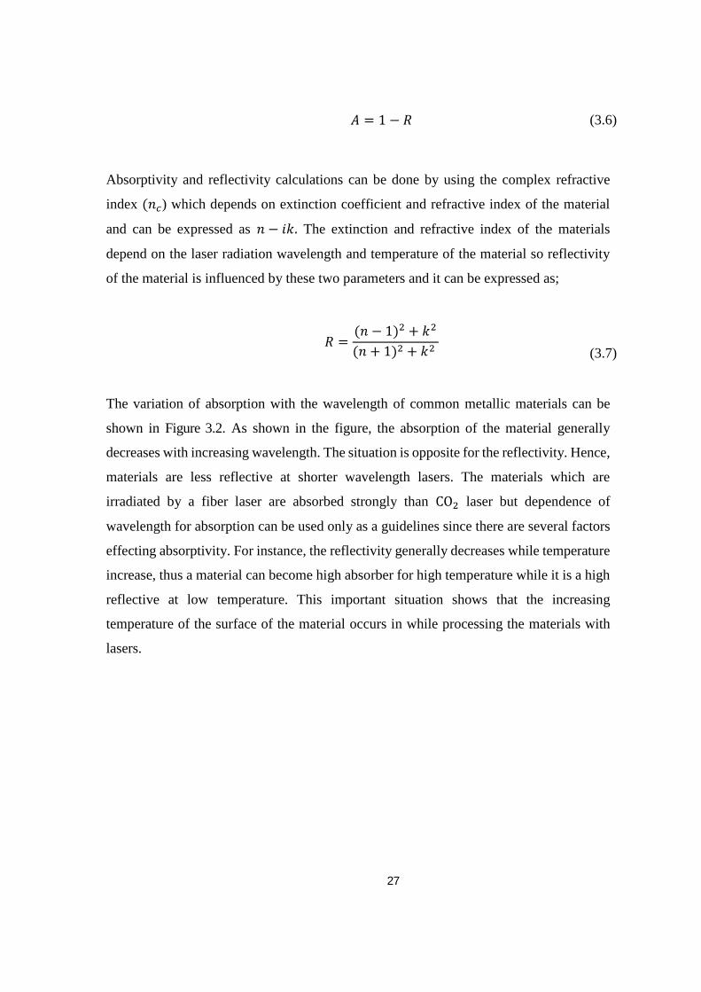
The variation of absorption with the wavelength of common metallic materials can be
shown in Figure 3.2. As shown in the figure, the absorption of the material generally
decreases with increasing wavelength. The situation is opposite for the reflectivity. Hence,
materials are less reflective at shorter wavelength lasers. The materials which are
irradiated by a fiber laser are absorbed strongly than CO2 laser but dependence of
wavelength for absorption can be used only as a guidelines since there are several factors
effecting absorptivity. For instance, the reflectivity generally decreases while temperature
increase, thus a material can become high absorber for high temperature while it is a high
reflective at low temperature. This important situation shows that the increasing
temperature of the surface of the material occurs in while processing the materials with
lasers.

28
Figure 3.2 The absorption of laser output at different wavelengths varies according to the
materials involved (adopted from [34])
The material which interacts with laser absorbs energy of the laser beam and then,
absorbed energy is transformed into heat by reduction of primary localized and ordered
excitation energy levels. The relaxation times of excitation energy levels are about 10−13
s for metals. After the conversion of the laser energy into the heat, the conduction process
and temperature sharing occur. During the material process, the degree of the temperature
and ionization of the vapor create physical effects in the material such as heating,
vaporization, melting, plasma formation and ablation. (Figure 3.3)

29
Figure 3.3 Effects after interaction of lasers with material. Orange arrows indicate heat
conduction.
The physical effects can be categorized into three groups as thermal effects, plasma
effects and ablation.
3.1.1 Heating
Heating process can be discussed by evaluating temperature distribution. The
analysis of the thermal behavior of the material can be solved via using one-dimensional
heat conduction equation which is indicated by Jager and Carslaw in 1959 [35]. In thermal
analysis, material is assumed as homogeneous, the temperature of the material is constant
at the beginning, heat is uniform during the radiation-material interaction and losses due to
radiation and convection are negligible. If we assume that a temperature 𝑇 is applied to
location z, the heat transfer equation after time 𝑡 can be shown as;
𝜕𝑇 (𝑧, 𝑡)
𝜕𝑡= 𝛼
𝜕2𝑇(𝑧, 𝑡)
𝜕𝑧2 (3.8)
where 𝛼 is thermal diffusivity.
The laser irradiation scheme for initial, heating and cooling times can be seen in
Figure 3.4.
30
Figure 3.4 Laser interaction with matter at different times: a) Initial condition where
temperature is uniform, 𝑇0, b) Laser heating process where surface temperature 𝑇𝑠 is higher
than initial temperature 𝑇0, c) Cooling of the material after laser off.
The initial condition of the temperature at 𝑡 = 0 can be written as;
𝑇(𝑧, 0) − 𝑇0 where 𝑧 ≥ 0 (3.10)
If we assume that, energy of the laser beam which is absorbed by the material surface is
equal to conducted energy, boundary condition at the surface can be written as;
𝛿𝐸𝑎𝑏𝑠 = −𝑘𝜕𝑇(0, 𝑡)
𝜕𝑧 (3.11)
where 𝐸𝑎𝑏𝑠 absorbed energy by the material, 𝑘 is the thermal conductivity. The equations
during the heating and cooling can be obtained. If the laser is on, the irradiation time 𝑡𝑝 ≥
𝑡 and if there is no any laser-material interaction, 𝑡 > 𝑡𝑝. While laser is on, ∆𝑇(𝑧, 𝑡)𝑡<𝑡𝑝
can be defined as;
𝐸𝑎𝑏𝑠
𝑘(4𝛼𝑡)
12 ierfc (
𝑧
(4𝛼𝑡)12
) (3.12)

31
In Eq. 3.12, 𝑖erfc(x) is the where ierfc is the integral of the complementary error function
and it can be written as ;
ierfc (x) =1
√𝜋{exp(−𝑥2) − 𝑥(1 −
2
√𝜋∫𝑒−𝜉2
𝑑𝜉
𝑥
0
) (3.13)
At 𝑧 = 0, for the equations 3.12 and 3.13, temperature of the surface while cooling and
heating of the material can be obtained;
∆𝑇(0, 𝑡)𝑡<𝑡𝑝 =𝐸𝑎𝑏𝑠
𝑘(4𝛼𝑡
𝜋)1/2
(3.14)
∆𝑇(0, 𝑡)𝑡<𝑡𝑝
𝐸𝑎𝑏𝑠
𝑘[(
4𝛼𝑡
𝜋)1/2
− (4𝛼(𝑡 − 𝑡𝑝)
𝜋)
1/2
] (3.15)
3.1.2 Melting
Depending upon the material, the surface temperature of the material which interact
with laser may reach the melting or boiling point at high or low power densities. The
melting and boiling thresholds are very critical while processing a material with high power
laser. After reaching melting temperature, the material stops raising its temperature, then it
gains an energy to melt a volume 𝑉𝑚𝑒𝑙𝑡 and energy equation can be described as;
𝐸𝑚𝑒𝑙𝑡 = 𝐻𝑓𝜌𝑉𝑚𝑒𝑙𝑡 (3.16)
2𝐸𝑎𝑏𝑠𝛼
12
𝑘
[
𝑡12 ierfc (
𝑧
(4𝛼𝑡)12
) − (𝑡 − 𝑡𝑝)12𝑖erfc
(
𝑧
(4𝛼(𝑡 − 𝑡𝑝))
12)
]
(3.9)

32
where 𝐻𝑓 is the heat of fusion and 𝜌 is density of the material. Hence, at an initial
temperature 𝑇𝑖, energy for melting a volume of material V is;
𝐸 = 𝐸𝑚𝑒𝑙𝑡 + (𝑇𝑚 − 𝑇𝑖)𝐶𝑝 𝜌𝑉 (3.17)
where 𝐶𝑝 is the specific heat and 𝑇𝑚 is the melting temperature of the material. The
maximum depth for a melting applications with constant pulsed lasers increases while laser
power density increases (Figure 3. 5a). If the pulse time of the laser increase at constant laser
power density, the depth of melting increases (Figure 3. 5b)
Figure 3. 5 The melting depths for pulsed laser applications. a) At constant pulse widths
b) At constant power density (adopted from [36])
3.1.3 Vaporization
The depth of melting of the material is limited by the maximum surface
temperature of the material so it is not possible to increase it to an infinitely large value

33
with high laser density. The maximum value of depth of melting 𝑍𝑚𝑎𝑥 is occured while
temperature of the material reaches the boiling point. 𝑍𝑚𝑎𝑥 can be calculated while
temperature at melting point 𝑇𝑚 by;
𝑇𝑚 =𝐸𝑎𝑏𝑠
𝑘(4𝛼𝑡)
12 ierfc (
𝑍𝑚𝑎𝑥
(4𝛼𝑡)12
) (3.18)
If the temperature reaches boiling point of the surface of the material, 𝑇𝑏 can be
calculated by;
𝑇𝑏 =
𝐸𝑎𝑏𝑠
𝑘(4𝛼𝑡
𝜋)1/2
(3.19)
The laser beam cause a liquid-vapor interface in order to move inside the material, after
vaporization is achieved at the surface. Then, material removing from the surface above
the interface of liquid-vapor is seen. The depth of the material, while vaporization process
occurs, can be derived by using velocity of the liquid-vapor interface 𝑉𝑠.
𝑉𝑠 =𝐸𝑎𝑏𝑠
𝜌(𝑐𝑇𝑏 + 𝐿𝑣) (3.20)
where 𝐿𝑣 is the latent heat vaporization. The mass of the removed material per unit time
(𝑚) is equal to 𝑉𝑠𝜌 and depth of vaporization (𝑑) is equal to 𝑉𝑠𝑡𝑝, thus;
𝑑 =𝐸𝑎𝑏𝑠𝑡𝑝
𝜌(𝑐𝑇𝑏 + 𝐿𝑣) (3.21)
3.1.4 Plasma Formation
After vaporization is initiated by irradiation of the material with high laser
intensity, evaporation of the surface occurs. After vaporization process, the vapor and the
laser beam on the material are important to understand and resolve comprehensive effects
of the laser material interaction. The vapor can be ionized and this effect is an important

34
interaction. In a gas environment, the Saha equation [37] can be used to define degree of
ionization by
𝜉
1 − 𝜉=
2𝑔𝑖
𝑔𝑎𝑁𝑔(2𝜋𝑚𝑘𝐵𝑇
ℎ2)3/2
𝑒(−𝐸𝑖𝑘𝐵𝑇
) (3.22)
where 𝐸𝑖 is the energy of ionization and 𝑔𝑖 is the degeneracy of states for ions and 𝑔𝑎 is
the degeneracy of states for the atoms or molecules. The total number densities of atoms
or molecules and electrons are defined as 𝑁𝑔. The ratio of densities of electrons and total
number densities of electrons give 𝑁𝑔.
The ionization can be partial or complete and it can be classified into two group
which are cascade (avalanche) ionization and multiphoton absorption. If the laser beam
energy is absorbed by seed electrons by bremsstrahlung absorption and energy of the free
electrons exceeds ionization energy of the molecules, the ionization process of the
molecules begins with collision (Figure 3.6a). The new electrons are achieved by the
ionization and photon energy is absorbed by these electrons. Hence, the breakdown
process (avalanche breakdown) starts. The plasma formation can be seen without any seed
electrons, interaction of particle and collision, thus collision of each electron is ionized
independently. This mechanism is named as multiphoton absorption (Figure 3.6b).
Figure 3.6 The laser induced breakdown mechanisms: ionization by a) avalanche
breakdown b) multiphoton absorption
35
3.1.5 Ablation
The removal of the material from the surface by photochemical and photo thermal
interactions can be defined as ablation. The laser energy absorbed by the material is
converted into thermal energy. If the energy of the laser beam is very high and the
temperature of the interacted part of the surface exceeds the boiling point, vaporization
and thermal stresses occur. The vaporization and thermal stresses cause the removal of the
material and this process is known as thermal ablation.
In organic materials, ablation process can occur by breaking of molecular bonds.
The molecular order of the organic materials can be broken, if the incident photon energy
is suitable for ablation of the material. This process is known as photo-chemical ablation.
The ablation process occur not only by bond-dissociation energy but also lower bond-
dissociation energy of material by the multi-photon absorption [36]. In this case, longer
wavelength incident photons with smaller photon energies are absorbed simultaneously
by two or higher number of photons, then they can break the bonds, although the energy
of the each photon is lower than bond-dissociation energy.
To understand ablation process in laser-material interaction applications, photo-
thermal and photo-chemical processes should be discussed together. The relaxation time
of thermal process (𝜏), which is related with dissipation of heat, is important to determine
long-short pulse relation. It can be defined by [38] ;
𝜏 =𝑑2
4𝛼 (3.23)
Where 𝑑 and 𝛼 show the depth of absorption and the thermal diffusivity, respectively. The
thermal relaxation time determines choosing pulse duration of the laser for a well ablation
with lasers so pulse duration is one of the key parameter for ablation process. If the pulse
time of the laser is longer than 𝜏, the laser energy is dissipated in the material. The material
is damaged by thermal process; if pulse duration of the laser is higher than of the thermal
relaxation time, short pulse durations result in the least dissipation.
One of the other parameters which affect the ablation of the material is pulse
repetition rate of the laser. The repetition of the laser keeps material in ablation zone if the
duration between the pulses is very short. Hence, high repetition rate is appreciated for an

36
efficient ablation process. The beam quality is another parameter which affects the
efficiency of material ablation with lasers. The laser beam energy should be delivered to
the ablation area efficiently by a controlled beam size in order to apply an effective
ablation.
In industrial material processing and medical applications, laser ablation is used for
marking, cutting, drilling, micro-machining, patterning and tissue ablation.
3.2 Temperature Effects in Pulsed Lasers
The defining thermal models for continuous wave lasers at constant intensity are
the easiest models among the laser operation types. The thermal analysis for pulsed
operation lasers is complex and depends on temporal shape of pulse and pulse width of
the laser beam.
A laser system with multipulse operation causes temperature increase on material
while each pulse interacts with the material. The generated pulses may be
different shapes such as rectangular, smooth, triangular or random (Figure 3.7). The
temperature of the material is affected by shape of the pulse. For instance, the higher
temperature is reached by rectangular pulses than other pulse types [37].
Figure 3.7 Different laser pulse shapes; a) rectangular, b) smooth, c) triangular, d)
random shapes.
After each interaction of the pulse with material, a cooling time takes place till interaction
of the next pulse. The cooling may not be enough for long pulse operation due to duration
between the pulses. The temperature of the material while subsequent pulses interact with
the material is higher than heating via prior pulses. Hence, the heating of the material for
pulsed laser-matter interactions depends on the heating and cooling time which is

37
determined by pulse duration and time between the pulses. The relation can be seen in
Figure 3. 8.
Figure 3. 8 Scheme of temperature difference on material surface during pulsed
operation a) single pulse, b) multipulse laser operation on material.
3.3 Special Instrumentation for Laser Material Processing
The outcome quality of the laser material processing applications depends not only on
the laser parameters but also on the careful instrumentation of the whole laser system. While
constructing a system, it is very important to choose appropriate instruments such as
galvanometric scanners and f-thetha objectives. The scan speed limits of the galvanometric
scanner specify the overlap of the pulses at different repetition rate. The objectives which are
used to focus laser beam, affect the depth of field and hence strongly influence of laser beam
on the processed material.
3.3.1 Galvanometric Scanners for Material Processing
The galvanometric scanner systems help the material processing applications to
achieve high speed and precise position on the material. They involve rotary motors which

38
direct focused laser beams onto target material. They are widely used in industrial
applications especially in marking, engraving, sintering, melting, drilling, scribing
process. Galvanometric scanners offer a number of advantages such as contact free and
precision processing, high speed, flexibility without retooling, elimination of the
mechanical tool wear. In today’s world, they are equipped with a closed loop position
control to achieve high scan speeds and precise laser process. The scanner consist pair of
mirrors which are rotated by servo amplifiers. The simple schematic of a laser processing
by galvanometric scanners is shown in the following figure.
Figure 3.9 The basic configuration of material processing with scan head
A commanded position data is created in computer and a digital interface included in a
control card is used to transfer data to scanner. There is a position detector inside the scan
head, it provides closed loop feedback to the control card. The control card compares the
data with actual position of the mirrors and adjusts current through the scan head to correct
for any variances. After output of the scan head, an F-theta lens is used to focus laser beam
to the material. The spot size and depth of focus is determined by the objective according
to equation 3.3.
3.4 Main Parameters
While processing materials with a pulsed laser generating nanosecond pulses, several
parameters such as pulse energy, pulse duration, peak power, power intensity are important for

39
the efficiency and quality of the processing. First, while pulse energy (𝐸𝑝) of the laser
increases, the depth of the processing area increase. It depends on the average power (𝑃𝑎𝑣𝑔)
and repetition rate of the laser pulses (𝑓𝑟) and is calculated by 𝑃𝑎𝑣𝑔/𝑓𝑟. Second, the pulse
duration (𝑡𝑝) is another factor which impacts the laser – material interaction duration. Third,
the peak power of the laser beam which depends on the average power, repetition rate and
pulse duration, is essential to overcome material processing thresholds. The pulse peak power
of the laser is calculated by 𝐸𝑝
𝑡𝑝. Fourth, power intensity of the laser depends on the average
power of the laser effective focal spot area (𝑐𝑚2). The calculation of the intensity of the power
density is :
𝑃𝑎𝑣𝑔 (𝑊)
𝐸𝑓𝑓𝑒𝑐𝑡𝑖𝑣𝑒 𝑓𝑜𝑐𝑎𝑙 𝑠𝑝𝑜𝑡 𝑎𝑟𝑒𝑎 (𝑐𝑚2). (3.24)
Also, fluence is used to calculate intensity of the laser beam by dividing the pulse energy by
the radiated area as;
𝐸𝑝 (𝐽)
𝐸𝑓𝑓𝑒𝑐𝑡𝑖𝑣𝑒 𝑓𝑜𝑐𝑎𝑙 𝑠𝑝𝑜𝑡 𝑎𝑟𝑒𝑎 (𝑐𝑚2) . (3.25)
Since intensity of the laser beam does not only depend on the first three parameters but depends
also on the optical configuration of the system (such as focal length of the laser, beam quality,
etc.), the optical configuration determines the response of the material to the laser beam more
dominantly than other basic parameters.

40

41
CHAPTER 4
DESIGN AND IMPLEMENTATION OF A 60 W PULSED FIBER LASER AMPLIFIER
In this chapter, development of the nanosecond pulsed ytterbium doped fiber laser
amplifier will be explained by discussing design and implementation parameters. First,
modulation of the pulses of the seed signal will be discussed, then amplification of the seed
will be explained by dividing each amplification stages. The fiber laser amplifier, which was
constructed for this study, is based on MOPA configuration so, several pre-amplifiers were
used to amplify power. The amplifier stage was divided into three stages as pre-amplifier,
middle amplifier and main amplifier. Pre-amplifier stage can be defined as a seed of middle
amplifier and it has two amplifier stages. In this chapter, all amplification processes are
explained from seed to free space laser output in detail. The whole system was characterized
by monitoring the spectrum and pulse shapes of the all stages. The nonlinear effects and ASE
at the output of the system will be characterized to achieve a spectrum without ASE and SRS.
Moreover, the components of the system were reduced, special electronic configurations and
mechanical case were developed for industrialization of the system. Hence, the system was
industrialized at the end of the experimental works.
4.1 Modulation and characterization of the seed signal
The fiber laser amplifiers with MOPA design is based on that a fiber laser
architecture is divided into a seed laser and an amplification stage. The electronic
modulation is an effective way to achieve controlled pulses from the seed of the laser.
The modulation allows to generate optical pulses by the modulation of the current
generator. The pulses of the system are created by modulation of the current of the laser
diode.
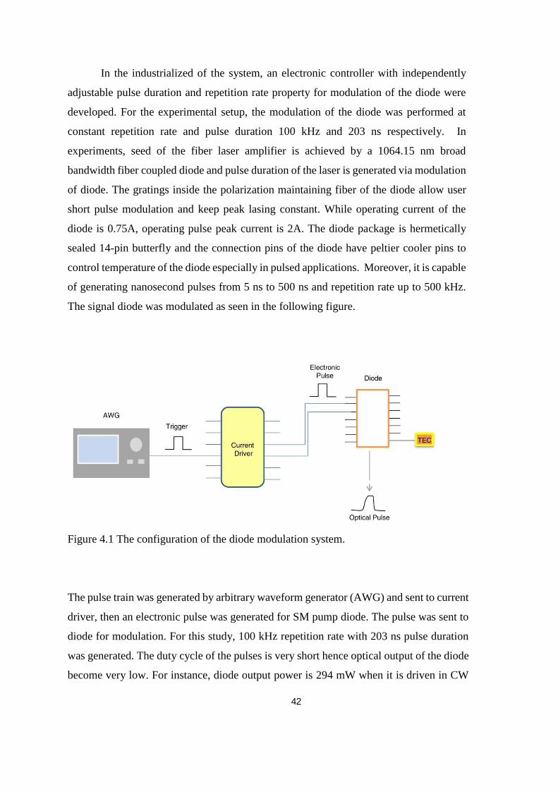
42
In the industrialized of the system, an electronic controller with independently
adjustable pulse duration and repetition rate property for modulation of the diode were
developed. For the experimental setup, the modulation of the diode was performed at
constant repetition rate and pulse duration 100 kHz and 203 ns respectively. In
experiments, seed of the fiber laser amplifier is achieved by a 1064.15 nm broad
bandwidth fiber coupled diode and pulse duration of the laser is generated via modulation
of diode. The gratings inside the polarization maintaining fiber of the diode allow user
short pulse modulation and keep peak lasing constant. While operating current of the
diode is 0.75A, operating pulse peak current is 2A. The diode package is hermetically
sealed 14-pin butterfly and the connection pins of the diode have peltier cooler pins to
control temperature of the diode especially in pulsed applications. Moreover, it is capable
of generating nanosecond pulses from 5 ns to 500 ns and repetition rate up to 500 kHz.
The signal diode was modulated as seen in the following figure.
Figure 4.1 The configuration of the diode modulation system.
The pulse train was generated by arbitrary waveform generator (AWG) and sent to current
driver, then an electronic pulse was generated for SM pump diode. The pulse was sent to
diode for modulation. For this study, 100 kHz repetition rate with 203 ns pulse duration
was generated. The duty cycle of the pulses is very short hence optical output of the diode
become very low. For instance, diode output power is 294 mW when it is driven in CW

43
regime at operating current 0.75A, while output of the seed laser is 0.48 mW at the same
current at 20 kHz repetition rate and 100 ns pulse duration. To overcome low output
problem, the diode was driven at 1.77A which is near the maximum pulsed peak current
by a current driver thus a sufficient seed signal was generated from the diode for
preamplifier. The seed signal power from the diode is very important for reliability of the
system. The temperature controlling of the diode is another important work, if the diodes
are operated at high current. To control temperature of the diode, thermo-electric cooler
(TEC), which controls the peltier inside the diode module, was used. The temperature data
set in microcontroller and TEC is operated with microcontroller by receiving temperature
data from it and stays temperature of the diode. The temperature controlling of the diode
is important for efficiency of the signal seed since the optical power of the diode decreases
at same current while temperature of the diode increases.
The modulation of the diode was characterized in different pulse duration steps by
adjusting duty cycle. Four different pulse durations which start from 203 ns to 407 ns
with about ~50 ns incrimination. While aiming to achieve high pulse energy and peak
power at the output of the amplifier, SRS power should be minimized. To minimize
nonlinear effects at the output of the system, there shouldn’t be spikes at pulse formation
of the seed signal. In this thesis, all characterization from preamplifier to output of the
whole system was characterized for 203 ns and the shape of electrical pulse generated
from current driver can be seen in Figure 4.2.
The optical pulse generated by using electrical pulse was measured and its shape
can be seen with the pulse train which measured at 100 kHz repetition rate in Figure 4.3.
As shown in figures, the shape of the optical pulse correspond to electrical pulse shape.
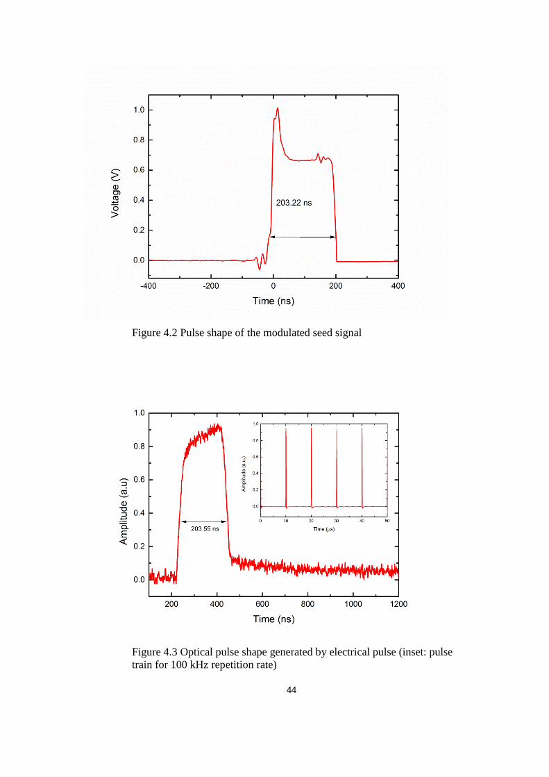
44
Figure 4.2 Pulse shape of the modulated seed signal
Figure 4.3 Optical pulse shape generated by electrical pulse (inset: pulse
train for 100 kHz repetition rate)

45
In this thesis, the duty cycle configured 200:1, which means it is ~200 ns pulse
duration at a repetition rate 100 kHz. The output power of the seed signal was
characterized with different repetition rates and pulse durations. The change of the output
power from the seed diode has shown while changing the repetition rate and pulse width
respectively in Table 4.1 The results show that increasing average power corresponds to
increasing repetition rate and pulse duration.
Table 4. 1 Output power of the seed diode with respect to different pulse durations and
repetition rates.
Power ( mW)
Repetition Rate
(kHz)
203 ns 254 ns 304ns 359 ns 407 ns
100 4.9 6 7.3 9 10.6
150 7.2 8.6 10.6 13.8 15.1
200 9.6 11.3 14 17.1 19.2
250 11.9 14.2 17.9 20.8 23.5
300 14.1 18.2 21.3 24.7 27.8
4.2 Preamplifier Design
The preamplifier of the system can be defined as a seed of the laser for middle
amplifier. To achieve a sufficient seed power for middle amplifier, two amplifier stages
were set in preamplifier. Theoretically watt level output instead of miliwatt can be
achieved in preamplifier stage by using only one amplification process from the seed
laser. The reason that construction preamplifier stage in two amplification process is that
high gain amplification from a low signal causes very high reflected ASE especially at
low repetition rates. Hence, it is possible to damage seed laser diode. Moreover, the
preamplifier was constructed by SM operation fiber in order to keep nearly diffraction
limited beam shape at the output of the fiber laser and this type of fibers can be damaged
at high level outputs. In addition, industrial fiber coupled SM components which are used
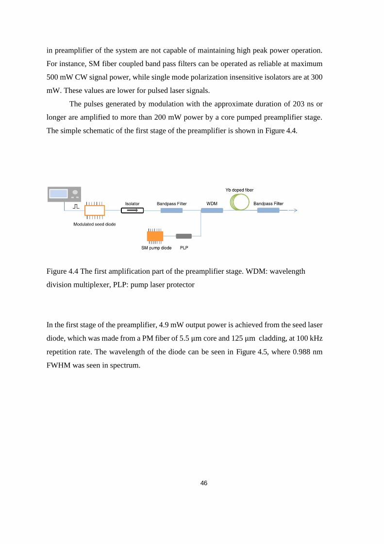
46
in preamplifier of the system are not capable of maintaining high peak power operation.
For instance, SM fiber coupled band pass filters can be operated as reliable at maximum
500 mW CW signal power, while single mode polarization insensitive isolators are at 300
mW. These values are lower for pulsed laser signals.
The pulses generated by modulation with the approximate duration of 203 ns or
longer are amplified to more than 200 mW power by a core pumped preamplifier stage.
The simple schematic of the first stage of the preamplifier is shown in Figure 4.4.
Figure 4.4 The first amplification part of the preamplifier stage. WDM: wavelength
division multiplexer, PLP: pump laser protector
In the first stage of the preamplifier, 4.9 mW output power is achieved from the seed laser
diode, which was made from a PM fiber of 5.5 μm core and 125 μm cladding, at 100 kHz
repetition rate. The wavelength of the diode can be seen in Figure 4.5, where 0.988 nm
FWHM was seen in spectrum.

47
Figure 4.5 Spectrum of the seed diode
The laser diode is protected from the back reflection and amplification which potentially
damages the seed laser diode, by a fiber coupled polarization insensitive isolator.
Moreover, backward amplification is a factor for reducing efficiency of the whole system.
The fiber coupled isolator has an operating wavelength ±5 nm at 1064 nm and its fiber is
HI1060 (mode field diameter of 6.2 𝜇m, 0.14 NA, 125 𝜇m cladding) which is a non-PM
fiber and has different core structures than diode fiber. In addition, insertion loss of the
isolator is 1.5 dB, thus splicing of diode and isolator with very low splice loss is very
important to achieve high transmission rate. To overcome splice loss from PM to non-PM
fiber splicing, longer arc-time with respect to same type of fiber splicing operated to the
non-PM fiber to increase its NA for coupling much seed signal from the diode fiber. An
efficient splice was achieved by 3.30 mW output power at the isolator output, hence the
most of transmission loss caused insertion loss of the isolator. After isolator component,
a 1064 nm fiber coupled band pass filter was used to protect diode from back reflected
ASE which is generated in amplification process. 3.21 mW power was measured at the
output of the band pass filter, after an efficient core to core splicing with isolator. The seed
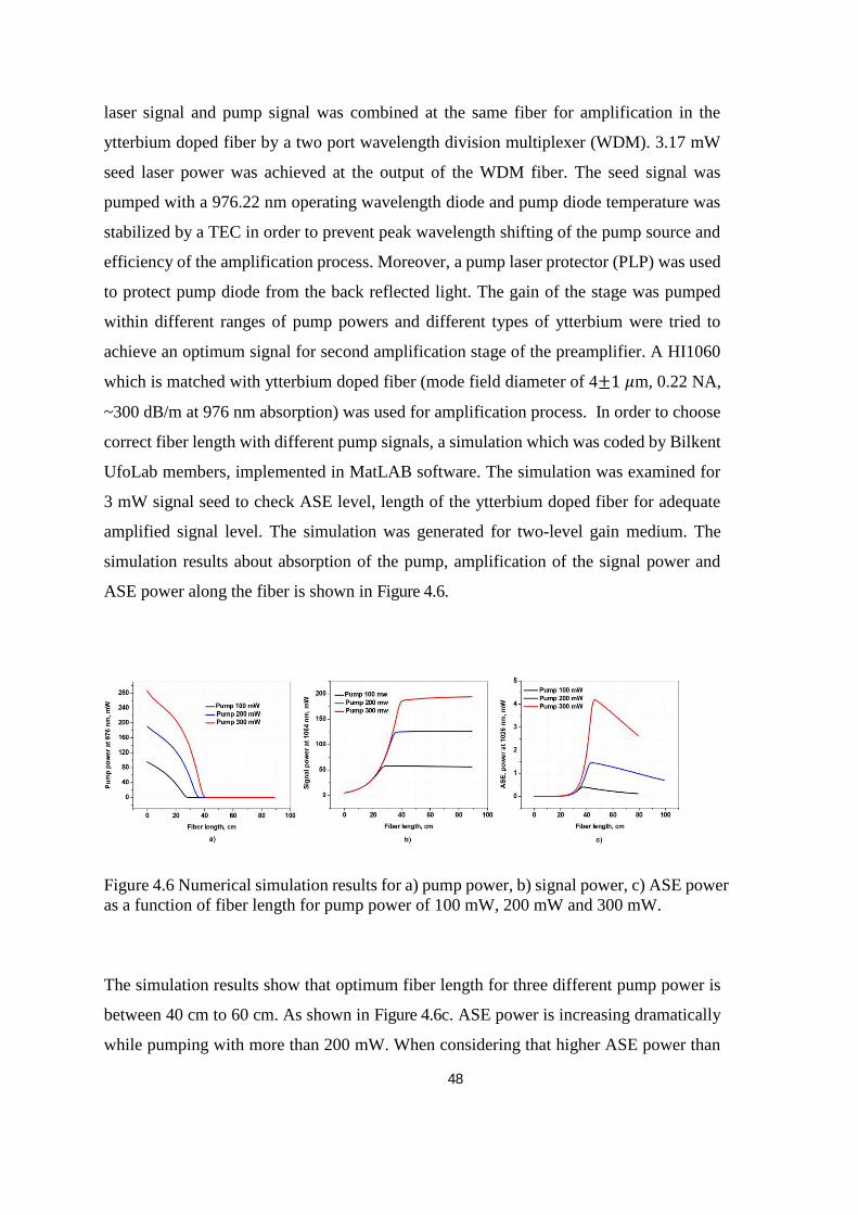
48
laser signal and pump signal was combined at the same fiber for amplification in the
ytterbium doped fiber by a two port wavelength division multiplexer (WDM). 3.17 mW
seed laser power was achieved at the output of the WDM fiber. The seed signal was
pumped with a 976.22 nm operating wavelength diode and pump diode temperature was
stabilized by a TEC in order to prevent peak wavelength shifting of the pump source and
efficiency of the amplification process. Moreover, a pump laser protector (PLP) was used
to protect pump diode from the back reflected light. The gain of the stage was pumped
within different ranges of pump powers and different types of ytterbium were tried to
achieve an optimum signal for second amplification stage of the preamplifier. A HI1060
which is matched with ytterbium doped fiber (mode field diameter of 4±1 𝜇m, 0.22 NA,
~300 dB/m at 976 nm absorption) was used for amplification process. In order to choose
correct fiber length with different pump signals, a simulation which was coded by Bilkent
UfoLab members, implemented in MatLAB software. The simulation was examined for
3 mW signal seed to check ASE level, length of the ytterbium doped fiber for adequate
amplified signal level. The simulation was generated for two-level gain medium. The
simulation results about absorption of the pump, amplification of the signal power and
ASE power along the fiber is shown in Figure 4.6.
Figure 4.6 Numerical simulation results for a) pump power, b) signal power, c) ASE power
as a function of fiber length for pump power of 100 mW, 200 mW and 300 mW.
The simulation results show that optimum fiber length for three different pump power is
between 40 cm to 60 cm. As shown in Figure 4.6c. ASE power is increasing dramatically
while pumping with more than 200 mW. When considering that higher ASE power than

49
simulation results in pulsed operation, maximum 100 mW pump source was applied to 60
cm Yb doped fiber for amplification process by forward and core pumping method. The
output power of the Yb doped fiber with respect to the pump power is shown in following
figure.
Figure 4.7 Pump power vs. output power from ytterbium doped fiber output.
The output power 42 mW was achieved from the Yb fiber output and a low level ASE
was seen from the spectrum of the Yb fiber output. A fiber coupled band pass filter which
works at nominal center wavelength 1064 nm, was used to eliminate ASE. After
elimination of ASE and transmission loss from the band pass filter and splice loss, 39 mW
output power was achieved at fiber output of the band pass filter. The spectrum of the
signal at the ytterbium fiber and band pass filter output is shown in the following figure.

50
Figure 4.8 Spectrum of the a) ytterbium doped fiber output (logarithmic scale)
The signal from the band pass filter was used to amplify second stage of the preamplifier.
Hence another amplification stage was used and its design can be shown with first
amplifier in following figure.
Figure 4.9 The preamplifier system

51
In the second stage of the preamplifier, Yb doped fiber was pumped by signal
which propagate from band pass filter to WDM where 0.32 dB signal loss from band pass
filter to WDM was seen due to splice loss and insertion loss of the WDM. Hence, 36, 3
mW signal was taken from the end of the WDM and it was pumped by 300 mW 976.09
nm SM pump diode for amplifying. A ytterbium doped (mode field diameter of 4. 4 ± 1
𝜇m, 0.22 NA, ~1200 db/m at 976 nm absorption) was used for amplification and length
of the ytterbium doped fiber was determined by using numerical simulations. The
numerical simulation results for second amplification stage of the preamplifier is shown
in the following figure.
Figure 4.10 Numerical simulation results for a) pump power, b) signal power, c) ASE
power as a function of fiber length for pump power of 100 mW, 200 mW and 300 mW
for the 2nd stage of the preamplifier.
The maximum saturated laser power from preamplifier stage was limited to 200 mW to
achieve an adequate signal in middle amplifier stage without ASE. In addition,
components at the end of the preamplifier stage work reliable at this power range. The
simulation results show that the maximum signal by pumping 300 mW pump power can
be achieved with a fiber more than 50 cm. To achieve low ASE spectrum at the output of
the ytterbium fiber 100 cm Yb doped fiber was used according to simulation results. After
pumping gain with ~300 mW, 237 mW signal power with a low ASE achieved at the
output of the ytterbium. The slope efficiency is 69.5% at this stage. The output power of
the Yb doped fiber as a function of the pump power is shown in Figure 4.11. The spectrum
of the ytterbium output can be seen in Figure 4.12.

52
Figure 4.11 The output power of the Yb doped fiber as a function of the pump power
Figure 4.12 Spectrum of ytterbium output (logarithmic scale), inset : linear scale.

53
ASE of the last stage of the preamplifier was eliminated by using a 1030 band pass filter
and after the elimination and splice loss, 227 mW signal was achieved at the band pass
filter output. To protect preamplifier stage, a 1064 nm 2W polarization independent
isolator was added to end of the preamplifier. The isolator has 0.41 dB insertion loss and
has a matched SM fiber with band pass filter so core to core splice was performed. After
isolator, 204 mW signal power was achieved. The spectrum of the preamplifier is shown
in Figure 4.13.
Figure 4.13 The spectrum of the preamplifier stage (logarithmic scale), inset: linear
scale.
4.3 Middle Amplifier Design
The signal achieved from the preamplifier stage was used to amplify an adequate
power for main amplifier stage. The multimode components was chosen to reduce
nonlinear effects, pump power and ytterbium length was chosen with caution to suppress
ASE. The simple schematic of the middle amplifier stage is shown in the following figure.

54
Figure 4.14 Simple schematic of the middle amplifier stage. CPS: Cladding pump
stripper, MPC: multi pump combiner.
After preamplifier stage a 99:1 SM fiber coupled coupler was used to detect seed signal
while laser is operating. The backward port of the coupler is used to detect back reflected
signal. The signal was combined with pump by using a (1+1)x1 multi-pump combiner
which has 10 μm core 125 μm double clad sized fiber. 164 mW output was achieved at
the end of the MPC. 10W multi mode pump which has 976 ±4 nm wavelength was used
to pump and it was protected by a MM PLP from the back reflection. A ytterbium fiber
(core diameter of 10.1±1 𝜇m, 0.07 NA, ~6.9 db/m at 976 nm absorption) was used as an
amplification gain. The ytterbium was pumped up to 7.5 W and the length of the ytterbium
for that pump power level was determined by simulations. First, simulation was performed
for the pump wavelength 976 nm which is maximum absorption level of the ytterbium.
The simulation result is shown in Figure 4.15.

55
Figure 4.15 Simulation results for determining length of the fiber at 976 nm pump power
As shown in the Figure 4.15, pump signal at 976 nm is absorbed by using 4 m ytterbium
doped fiber. The length of the ytterbium was chosen by the help of simulation results so
4 m ytterbium fiber was used for amplification process. 4.2 W power was achieved at
ytterbium fiber output, however it involve a slightly pump power since some of the pump
power cannot be absorbed by ytterbium fiber due to variable wavelength of the MM diodes
at different temperatures or imperfect splice between preamplifier and middle amplifier
stage. The multimode diodes which are used in that stage have 976 nm central wavelength,
however it may change due to variation of temperature at different operating currents and
environment. The changing wavelength means changing absorption of the pump. Thus,
the simulation was performed for different wavelength 972 nm and 978 nm since MM
diodes have 4 nm bandwidth and the peak wavelength which changes according to
temperature of the environment and operating current of the diodes.
Hence, it is possible to detect a high level unabsorbed pump power for different
wavelength. The results of simulations for 972 nm and 980 nm pump wavelength is shown
in the following figure.

56
Figure 4.16 Simulation results for a)972 nm pump wavelength b) 980 nm pump
wavelength.
Another reason which causes unabsorbed pump is imperfect mode matching while
splicing fibers [41]. There are several splices which present in a whole fiber laser system,
so the pump leakages from core to cladding may occur after a poor performance splice.
Hence a long pass filter after ytterbium fiber was used to measure exact signal output from
the ytterbium output. The signal with respect to pump graph is shown in the following
figure.
Figure 4.17 Measured signal power as a function of pump power.

57
After pumping ytterbium doped fiber by 7500 mW pump power, more than 200 mW
unabsorbed pump eliminated by a long pass filter which only transmits photons higher
than 1000 nm wavelength. In real system, elimination of unabsorbed pump power is very
important since it may causes damage to fiber by localization of the heat at cladding. It
is also important to reach a high beam quality laser output since laser output with residual
pump reduce the quality of the beam. In addition, the reliability of the components are
affected by the unabsorbed pump. There are several ways to eliminate unabsorbed pump
from an all fiber laser amplifier. First, ytterbium doped fiber can be chosen longer than
that of used in this stage. However, longer ytterbium causes nonlinear effects. The second
way is using a temperature controller to keep diode at constant temperature but it’s very
difficult for a high power diode. This is because the MM industrial diodes have small
case and it is very difficult to keep their cases at constant temperature especially at
operating current. Third way is using a grating stabilized MM diode which have constant
wavelength even in high temperatures, however they are new diode technology for high
outputs and very expensive components. Fourth, using a cladding pump stripper (CPS) is
a way to eliminate unabsorbed pump signal from the amplifier. In this design a CPS was
developed for stripping unabsorbed pump. The schematic of the CPS is shown in the
following figure.
Figure 4.18 Design of the CPS
To develop CPS, a 10 um core 𝜇m core and 125 𝜇m clad sized double clad fiber were
used. The cladding of the fiber has a refractive index of 1.45, so the environment with

58
higher refractive index than clad can be developed for elimination of the unabsorbed
pump. Hence the middle of the fiber coating and outer cladding was stripped and the
unabsorbed pump which propagates at the cladding was eliminated by injecting an index
matched gel to that region. The gel, which is colorless, clear and a kind of liquid
photopolymer, has refraction index of 1.56. It is curable by UV light and it was used to
recoat inner cladding of the fiber. The difference of the refractive index between the inner
clad and recoated region assists to eliminate the residual pump power. After elimination
process, 210 mW pump power was eliminated at middle amplifier stage of the fiber laser
system. The spectrums of output of the ytterbium fiber and output of the CPS component
at the operating current of the system is shown in the following figure.
Figure 4.19 The spectrum of the ytterbium fiber output, inset: CPS output.
4.4 Main Amplifier Design
In the last stage of the fiber laser amplifier, the signal achieved from the middle
amplifier stage was used for amplification process. After amplification process, more than

59
60W signal power and 0.6 mJ pulse energy were achieved with a high beam quality and
good pulse-to-pulse stability. The output of the amplifier was characterized, long time
tests were performed and stability of the laser parameters were observed. In this stage, it
is possible to happen several challenges, such as splicing different cladding size fibers,
reaching high beam quality, temperature stabilization of the MM diodes, elimination of
the ASE and SRS, since reaching a high power laser output is a compelling way. Hence,
several methods were created to solve challenges in different region of the main amplifier
and they were explained in details. The simple configuration of the main amplifier is
shown in the following figure.
Figure 4.20 Simple schematic of the main amplifier of the system.
In this stage, a 25 μm core size and 250 μm cladding size double clad fiber input MPC
was used to combine pump and signal power. Hence it is very important to achieve a low
loss splice while splicing it with a 10 μm and 125 μm cladding size fiber which was used
at the output of the middle amplifier. A commercial Fujikura FSM 100 splicer was
employed to splice large and small diameter fibers. To achieve a low losses splice result
with splicing different cladding sized two fibers, arc region was chosen on the 250
μm cladding size fiber instead of center of the two fibers. The reason is that large cladding

60
size fiber needs high arc power which is too much for a 10 μm fiber and it damages the
fiber core and cladding structure while splicing. Hence, large diameter fiber were shifted
300 from the arc center and arc was applied to that region of the large diameter fiber.
Moreover, NA of the large diameter fiber was increased in this way, hence coupling of
the pump and signal was enhanced. The demonstration of the splicing process and image
of the splice of different diameter fibers are shown in Figure 4.21b.
Figure 4.21 a) Simple schematic of the fiber splice, b) splice image of middle amplifier
output fiber to MPC input fiber of the amplifier.
After splicing of middle amplifier with main amplifier stage, 4.08 W power was achieved
at the output fiber of the MPC which has a same core/clad diameter with input. A high
doping concentration ytterbium doped fiber (10.8 dB/m absorption at 976 nm) was chosen
to amplify signal to keep fiber length short since the short fiber length provides to avoid
nonlinear effects. The length of the ytterbium doped fiber, which has same core and
cladding size with MPC output, was determined after characterization of the pump diodes.
In this stage, four MM fiber coupled diodes whose maximum output power is 25W (975
±5 nm bandwidth, 0.15 core NA) were used to pump active medium by clad pumping.
The diodes have protection filter inside so PLP components were not used. The pump
diodes’ central wavelengths depend on the operating current, wall plug efficiency,
temperature of the environment and optical design. The temperature of the diodes
increases with increasing applied current hence the central wavelengths shift. Driving

61
current dependency of the central wavelength of the diodes at room temperature is shown
in the following figure.
Figure 4.22 Measured maximum emission wavelengths of the diodes as a function of
applied current at room temperature.
Hence, it is very important while choosing ytterbium doped fiber length, to perform a
simulation for different pumping wavelengths. Fiber length should be analyzed for all
different wavelengths and chosen optimal in regard to avoid from ASE and SRS. The
simulation results of ytterbium doped fiber which is pumped with four different pump
central wavelength diodes as a function of ytterbium doped fiber length are shown below.

62
Figure 4.23 Simulation results for amplifier stage at different pump wavelengths at a)
970 nm b) 973 nm c) 976 nm d) 979 nm
The length of the ytterbium doped fiber was chosen as 7 meter via simulation results. It
was thought that, elimination of unabsorbed pump power lower than 2 W is easy by the
help of CPS and single clad fiber at the end of the system. After choosing the length of
the ytterbium doped fiber, it is very important to achieve a low loss splice between
ytterbium doped fiber and MPC. Ytterbium doped fiber was spliced to MPC by improving
a special splice technique to achieve core to core splicing. In this stage, it’s very important
to achieve core to core alignment between ytterbium and passive fiber while splicing since
leakage of the high intensity pump may damage the fiber coating or leakage of the signal
from core to clad may amplify inside the cladding [42].
It’s difficult to detect core of the ytterbium doped fiber by a splicer camera since
its core geometry is octagonal. To overcome this problem, ytterbium doped fiber’s coating
was stripped and an arc power was applied to it in the splicer to change its geometry from

63
octagonal to round. After arc process, it was cleaved and prepared for core to core splicing
and a low loss splice process was achieved. The image of splicing which was taken from
the splicer after core to core splicing is shown in the following figure.
Figure 4.24 Splice image of MPC output fiber with ytterbium doped fiber.
Then, splice point was recoated with an UV curable flexible polymer gel whose refractive
index is 1.33, to couple potential pump leakage and to protect this region from the external
factors.
The diodes were spliced to (6+1)x1 MPC and operated 25 W of each by cooling
on a heat sink. Ytterbium doped fiber was cleaved 8̊ to protect middle and preamplifier
from back reflected light and output of the system was measured from that point at
different pump levels. While pumping with different pump power levels, it’s possible to
encounter residual pump problem as encountered at middle amplifier stage. To develop a
long time operational fiber laser system without a strict temperature control, elimination
of the residual pump by a CPS was preferred. The residual pump at the end of the system
was measured by using a long pass filter which only transmits 1000 nm and higher
wavelength photons. To protect system from the residual pump, another CPS was
developed as did at middle amplifier stage. A double clad 30 cm passive fiber was used.
The fiber core and clad size, NA of the fiber core and clad preferred same as ytterbium
doped fiber which was used in this stage. The fiber’s jacket and outer cladding was
stripped along 4 cm in the middle of it. The high refractive index (1.56), UV curable liquid
photopolymer gel was injected and to that region and cured. After development of the
CPS, it was spliced to ytterbium doped fiber by using same splice technique as splicing
MPC to ytterbium. Output of the ytterbium doped fiber was measured 2.7 W, while middle

64
amplifier being operated. Then, active medium of main amplifier stage was pumped at
different pump levels to detect residual pump levels. The elimination of the pump power
for different pump levels by long pass filter and CPS respectively is shown in the
following figure.
Figure 4.25 Residual pump at ytterbium fiber output as a function of pump power.
The active medium of the main amplifier was pumped by maximum 94.5 W pump power
and output of the spectrum was characterized for different pump levels. The maximum
output signal power from the CPS fiber was measured 69.1 W with a slope efficiency 76%
at this pump level. Signal power at the output of the CPS fiber as a function of pump
power is shown in the following figure.

65
Figure 4.26 Measured signal power as a function of pump power at CPS fiber output.
For the protection of the whole system from back reflected signal while processing
material, a 70 W collimated high power fiber coupled isolator was used. The nominal
output beam diameter of isolator is 3.8 and it was enlarged by a beam expander to 8 mm.
The eccentricity and ellipticity of isolator are 0.5 and 90 respectively. The fiber of the
collimated isolator was chosen single clad (25 μm core and 250 μm cladding size, 0.07
NA) to eliminate possible residual pumps due to CPS-isolator splice. The transmission
loss of isolator (0.3dB) and coiling of ytterbium fiber radius chosen 5 cm, hence
transmission loss and coiling radius led a decrease in signal power to 60.4 W signal power
at the output of the collimated isolator. The transmission loss of isolator (0.2dB) and loss
at 5 cm coiling radius led a decrease in signal power to 60.4 W signal power at the output
of the collimated isolator. The measured signal power as a function of pump power is
shown in the following figure.

66
Figure 4.27 Measured power as a function of pump power at the output of the collimated
isolator.
4.5 Characterization of the output signal
The whole amplifier and output signal of the system is characterized from various
parameters such as beam quality, pulse duration, long term and pulse stability, spectrum
of the signal for different parameters. In this section, all characterization process and
characterization techniques will be discussed.
4.5.1 Pulse Duration
The pulse duration of the system was characterized as 204 ns square pulse at the
beginning of the seed diode. While a square pulse is amplified in a high gain medium, the
tail of the pulse amplify lower leading edge of the pulse [43]. Hence, a significant
distortion of the pulse occurs at the output pulse. The distortion of the pulse causes pulse
shaping with amplification gain at leading edge of the pulse lead high peak power. There
is a relation between pulse energy 𝐸(𝑡) and effective mode area of the fiber 𝐴𝑒𝑓𝑓 as;

67
𝐸(𝑡) = ∫ 𝐴𝑒𝑓𝑓 𝐼(𝑡)𝑑𝑡 = 𝐴𝑒𝑓𝑓𝑈(𝑡)𝑡
𝑡0
(4.1)
where 𝐼(𝑡) is the signal intensity and 𝑈(𝑡) is the energy per unit area. If the input pulse is
square the output pulse of the system can be calculated by
𝐺(𝑡) = 1 + (𝐺0 − 1)𝑒−𝑈𝑜𝑢𝑡/−𝑈𝑠𝑎𝑡 (4.2)
where 𝐺(𝑡) is the time-varying gain at any instant time and output pulse can be
calculated by;
𝐼𝑜𝑢𝑡 = 𝐼𝑖𝑛(𝑡)𝐺(𝑡) (4.3)
The pulse duration of the system was characterized for different power and different
repetition rates. First, the pulse durations was measured at different output powers, while
repetition rate is 100 kHz as shown in the Figure 4.28. Second, they are measured when
repetition rate of the system changes in 20 kHz interval from 100 kHz to 300 kHz as shown
in Figure 4.29. At highest peak power, 29 ns effective pulse duration (FWHM) was
reached. The pulse width (FWHM) and shaping of the gain can be tailored to material
processing application needs.

68
Figure 4.28 Pulse shapes at different output powers at 100 kHz repetition rate
Figure 4.29 Pulse shapes and durations at different repetition rates at constant (60W)
average power.

69
4.5.2 The spectra
The collimated isolator fiber was kept 2 m long and maximum peak power is 20
kW. The peak power, length and core size of the delivery fiber affect the SRS level (Eq.
2.22). Therefore, when the peak power increased, SRS was seen in the spectrum. While
the peak power of the system is increased, it reaches SRS threshold and energy of the
signal starts to transfer its energy to the nonlinear components. The spectrum of the system
was measured at different pump levels by Anritsu MS9740 optical spectrum analyzer to
analyze nonlinear and spontaneous emission behavior of the systems. After 14 kW peak
power level, SRS starts and it became a large amount at 20 kW peak power since the
spikes are formed at beginning of the pulse when the peak power is high and the pulse
distortion become higher above the SRS threshold. For instance at 60 W average power
level, peak of the pulse consists of higher SRS than other pulses. At maximum operating
current, first order SRS which is 32 dB lower than peak was measured. The spectrum of
the system for different signal powers at 100 kHz repetition rate is shown in the Figure
4.30. On the other hand, SRS decreases with increasing repetition rates since interaction
peak power of the laser beam and distortion of the pulses decreases. In addition, SPM
broadens the bandwidth of the spectrum as the peak power increases and a slight spectral
enlargement at 1064 nm was observed. The ASE level of the amplifier is also very low.
The spectra of the system at full power and different frequencies are shown in the Figure
4.31.

70
Figure 4.30 The optical spectra of the output signal for 20,30,40,50,60W powers. (inset:
logarithmic scale).
Figure 4.31 Spectrum of the signal at 60 W with different repetition rates. (logarithmic
scale).

71
4.5.3 The beam quality
The brightness of the output signal of the system is determined not only output power but
also beam quality. The non-linear effects can be diminished by using high core diameter;
however this lowers the quality of the beam since transverse modes besides basic mode
are guided inside the fiber core [44]. The beam quality (M²) factor of the system was
measured by using a CCD camera beam profiler (Thorlabs BC106N-VIS) for different
signal powers according to 4 Sigma Diameter ISO11146 standard. [45]. The standard
includes a fitting procedure to the measured beam radius along the propagation direction.
In this thesis, a nearly diffraction limited M² was aimed. For this purpose, optimization of
the minimizing thermal effects and coiling of the ytterbium doped fiber at the amplifier
stage is very important. To achieve high beam quality, higher order modes were
suppressed by coiling technique. The technique is not practicable for high NA and core
diameter fiber. Our fiber type at the amplifier stage is applicable for using coiling
technique. The characterization of M² was performed for different coiling radius of the
ytterbium doped fiber and minimum 1.51 M² was achieved. While the middle and main
amplifier gain medium of the system is cooled, the beam quality factor as a function of
coiling radius of ytterbium doped fiber is shown in the Figure 4.32.
The maximum beam quality of the system while system is operated at maximum
power and active mediums of middle and main amplifier were coiled 5 cm radius and
cooled, is measured 1.52. The measured beam quality and 2D and 3D profile of the beam
are shown in the Figure 4.33 and Figure 4.34 respectively.

72
Figure 4.32 The beam quality factor as a function of coiling radius of ytterbium doped
fiber.
Figure 4.33 Beam quality factor measurement at maximum operating power.

73
Figure 4.34 Beam profile of the laser output a) 2D profile, b) 3D profile
4.5.4 Long Term Power Stability
The long term power stability of the system at maximum average power was
measured by operating system for 200 minutes. The output of the system was measured
by a thermal sensor with Thorlabs PM320E power meter and output power data was
recorded at 10 s interval up to 200 minutes. The laser output power was reached to 60.4
W average power after 10 minutes, then it decreased to 60.2 W after 80 minutes because
temperature of the diodes led wavelength shifting of the pump signal. Hence, after system
reaches its steady state value, change in output laser power became less. The change of
the output power divided by output power is shown in the following figure.
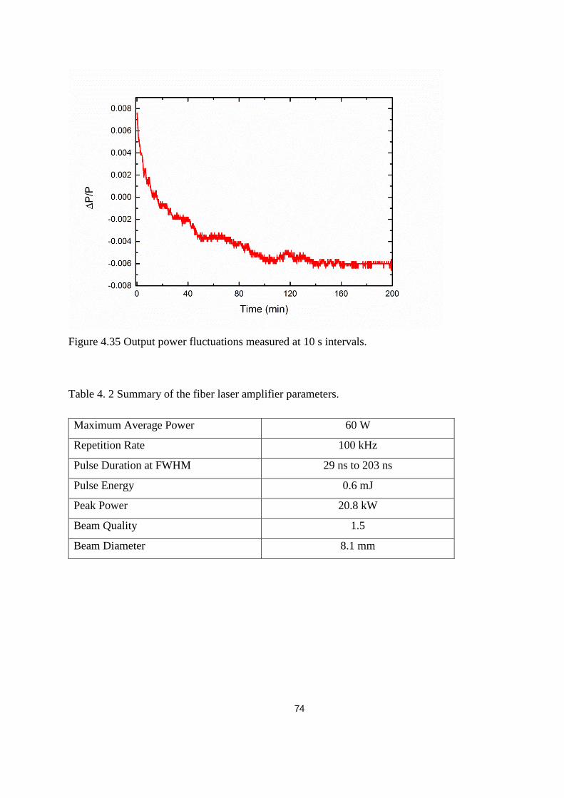
74
Figure 4.35 Output power fluctuations measured at 10 s intervals.
Table 4. 2 Summary of the fiber laser amplifier parameters.
Maximum Average Power 60 W
Repetition Rate 100 kHz
Pulse Duration at FWHM 29 ns to 203 ns
Pulse Energy 0.6 mJ
Peak Power 20.8 kW
Beam Quality 1.5
Beam Diameter 8.1 mm

75
Figure 4.36 Photo of the experimental setup
4.6 Industrialization of the Fiber Laser Amplifier
The developed fiber laser amplifier was industrialized by casing in a compact
module for material processing applications. To industrialize an output of a research and
development process, several factors should be considered together. First, it is very
important to reduce number of components in order to reduce the case of amplifier.
Second, choosing high reliable components provides a reliable long term operation to
amplifier. Third, managing thermal flow inside the case is important to increase reliability
of the amplifier since efficiency of the diodes and laser medium are affected from high
temperatures. Fourth, designing the electronic controllers and cards is important for they
should be small and reliable for providing pulse and current generation. Therefore, a
compact laser amplifier was developed by taking into all of these factors.
To achieve modulated signal from SM pump diode, I had electronic control card
that was developed by METRA Electronics. The card has an input for providing signal
frequency to the diode and a microcontroller to determine the duration of the pulse. The
important specification of the card enable changing pulse duration while the repetition
rate is constant The trigger signals generated by a pulse generator are sent to
microcontroller and the duration of the generated pulse is determined by the user from
200 ns to 500 ns in 50 ns interval independently from repetition rate. After switch on the
electronic card, it starts from 200 ns pulse duration. To control pulse duration, a pulse
width controller was used and it sent command to the microcontroller according to

76
determination of the user. The modulated signal is sent to current controller and a
modulated current is provided to the diode. Then, pulse duration is generated by the
modulated current. Moreover a current driver for SM pump diode and a current driver for
MM pump diodes are integrated on the card. The current of the diodes is set at operating
current by a control knob. In addition, circuit of the electronic card include a TEC (thermo
electronic cooler) for providing a constant temperature to the signal diode and pump diode.
Another electronic card with TEC was developed to cool SM pump diode. A simple
schematic of the control card is shown in the following figure.
Figure 4.37 Simple schematic of the signal modulation mechanism in electronic card.
The same current as experimental setup was applied to current controller and same
output was achieved. In preamplifier design, one pump module with 400 mW output
current was used as different from experimental setup. 400 mW pump power was divided
to ~300 mW and ~100 mW by using a 25/75 single mode fiber coupled coupler. The
configuration of the preamplifier is shown in the following figure.

77
Figure 4.38 Industrialized design of the preamplifier stage.
In preamplifier, while switch on button is used to activate modulated seed diode
and SM pump diode, they are operated simultaneously at operating current.
A 630/1064 nm coupler was used between middle and preamplifier stage in order
to add a 635 nm SM diode to guide processing area on the material. A control card, which
operates at 5V and limits the current of the circuit for 630 nm diode, was developed and
the diode was integrated on it. Then system design was re-constructed to straiten the area
of components. It is easy to decrease and stabilize the temperature of the cooling zone
by five 5200 rpm fan if the temperature is distributed homogenously. Hence a 310 x 255
mm aluminum cooling profile with air blast cooling was used to cool diodes at operating
current. The diodes were placed homogenously on the cooling zone. The ytterbium doped
fiber of the middle amplifier stage and fiber of the other components were placed into a
thermally conductive silicone adhesive. The cooling zone was also used to cool ytterbium
doped fiber, PLP and MPC of the middle amplifier stage and ytterbium doped fiber and
MPC of the main amplifier stage. A current driver which is integrated with electronic
control card was used to drive all five MM pump diodes which were connected serially.
While increasing pump level of the middle amplifier stage, pump power of the main
amplifier stage also increases. This situation provides a low ASE level in low power
levels. A simple schematic of the whole system is seen in Figure 4.39.
The current driver of the pump diodes operates with a signal between 0-5 V and
generates maximum 10.5 A. It can work at 30 V operational voltage. The design of the

78
electronic control card allows to get signal in order to operate pump driver externally. An
input was taken on the case of the laser amplifier system for external power control.
Figure 4.39 A simple schematic of industrial system.
Ytterbium doped fiber of the main amplifier stage was placed into a fiber coiling
stage with an thermally conductive adhesive and a fan was used to cool fiber and inside
the amplifier case. Total dimension of the laser amplifier case is 310 x 155 mm x 250 mm
and this dimension consists of not only amplifier source but also electronic control card
of galvanometric scanner. The mechanical case has 4 buttons in front of it. While two of
them allow the user to open preamplifier and amplifier respectively, the others allow
controlling pulse width of the laser beam. A 7-segment display was used to show pulse
duration of the system. When laser amplifier is opened, 7 segment display on with 0
indication which means pulse duration is 200 ns. Each incrimination of 1 means increasing
a 50 ns pulse duration. Another two LED display “ready” and “mark” was used on front
face of mechanical case. While laser is ready for operation, ready led on. On the one hand,
mark display become on if laser amplifier is active. After constructing all electronic

79
configuration, a wall plug efficiency 28% was achieved. One of the advantage of the
system is that if fiber length of the amplifier and signal seed in amplification stage are
chosen right, its MOPA design allow us to upgrade its average power by only adding
pump diodes to amplifier without changing design of the whole system.
Photograph of the industrialized laser amplifier and whole system with power
supply and galvanometric scanner is shown in the following figures.
Figure 4.40 The industrialized laser amplifier.

80
Figure 4.41 Laser system with galvanometric scanner.
4.7 Comparison with other industrial systems
There are some of fiber laser manufacturers in the world and a few company has
an ability to develop all fiber nanosecond pulsed MOPA structure with more than 50 W
average power laser amplifier. The most known companies that develop and sell pulsed
MOPA configuration fiber laser more than 50 W average power are SPI Lasers [46] and
Max Photonics [47]. As shown in the following table, developed fiber laser in this study
has several advantages in comparison to others in industry. It is clearly seen that the beam

81
quality of our laser amplifier is better than others while pulse energy is lower. Despite
lower pulse energy, lower pulse duration provides higher peak power than others. On the
other hand, pulse duration range, output power stability and weight of mechanical case
are preferable to others.
Table 4. 3 The parameters of other industrial MOPA lasers
Specifications SPI RM 50 SPI RM 70 SPI 70HS MP MFPT 50 MP MFPT70
Average power
(W)
50 70 70 50 70
Max. pulse energy
(mJ)
0.5 >1 >1.25 0.91 0.91
Beam quality <1.6 <1.6 2.5-3.5 <2 <2
Pulse width range
(ns)
40-260 40-260 10-250 10-250 10-250
Peak power >10 >10 >20 NA NA

82

83
CHAPTER 5
MATERIALS PROCESSING WITH FIBER LASER AMPLIFER
Materials processing with a pulsed fiber laser is a very common technique for
many different application areas and several types of the lasers are demonstrated in the
literature to show laser-material interaction behaviors on the material by drilling, scribing,
marking, cutting, engraving and marking. The most of the pulsed fiber lasers in materials
processing area relies on Q-switch configuration. In this configuration, external crystals
are used to releasing and storing the energy, however these types of laser are limited by
the Q-switch technology. This limitation causes an inflexibility of the pulse energy, pulse
duration and repetition rate. In addition, there are lots of studies for material processing
applications but it is also limited with regard to the target material. The developed MOPA
design fiber laser amplifier in this study have some special properties such as
independently adjustable pulse duration and repetition rate, nearly diffraction limited
beam quality, high peak and average power, all fiber design, and pulse to pulse stability.
In this chapter, by using several materials and applications, there will be discussions on
how these properties are related with each other while processing of the materials with
laser and performance of the developed laser amplifier.
5.1 Introduction
To process materials, several setup configurations were used, however all of them
are mainly parallel to configuration showed in Figure 3.9. While several configurations
are used, effects of the main parameters such as average power, pulse energy, pulse
duration, repetition rate, focal length of the objective and scan speed are characterized
according to materials and applications. Hence, all of these parameters has different
effects in processing. If pulse energy, pulse duration and peak power parameters are changed
individually, it is very easy to determine effects of them on the materials. While processing the

84
materials with pulsed lasers, adjusting pulse overlapping with scan speed and repetition rate
and spot diameter of the beam are also very important. A demonstration for pulse overlapping
is shown in the following figure.
Figure 5.1 The demonstration of the pulse overlapping.
The gray area is pulse overlap area and L is the distance from center to center. The L value can
be calculated by 𝑠𝑐𝑎𝑛 𝑠𝑝𝑒𝑒𝑑 𝑟𝑒𝑝𝑒𝑡𝑖𝑡𝑖𝑜𝑛 𝑟𝑎𝑡𝑒 (𝑝𝑝𝑠)⁄ , d is the laser spot diameter and S is
the length of overlap. Then the percentage of pulse overlapping can be calculated by
𝑂% =𝑠
𝑑= [1 −
𝐿
𝑑] × 100 (4.1)
The scan speed and repetition rate were changed in different applications, this means it is very
important to choose best overlapping result for each process. In this study, 100 mm and 160
mm focal length objectives were used to focus laser beam. For the 160 mm and 100 mm focal
length objective, the spot diameter of the developed laser is 38 μm and 25 μm respectively.
The percentage of the overlapping of pulses of developed fiber laser amplifier for different
repetition rate and scan speed was calculated for each material processing applications. For

85
instance, the overlapping percentage for 160 mm objective as a function of repetition rate of
laser with different scan speed is shown in the following graph.
Figure 5.2 Percentage of pulse overlap as a function of repetition rate in different scan
speeds.
The pulse to pulse stability on the material is another important factor and it was controlled
visually by using a setup as Figure 3.9 and a bulk silicon was scanned by with 160 mm
objective by repetition rate of 100 kHz laser beam and two different scan speeds of 3800 and
2200 mm/s. The surface of the bulk silicon was inspected by scanning electron microscope
(SEM). The formation of the pulses with different scan speed is shown in Figure 5.3. As shown
in the figure, adjusting scan speed of the laser beam is very important in processing the
materials. In this section, all of laser parameters were characterized for different material types
and capability of the laser is explained by processing different material and characterizing of
laser processing parameters for each of them.

86
Figure 5.3 Pulse to pulse formation at 100 kHz repetition rate on the material with
scanning speed a)3800 mm/s b) 2200 mm/s.
5.1.1 Microdrilling Efficiency
In this section, comparison of different pulse durations of laser beam effect on two
different material targets with same thickness such as stainless steel and aluminum was
performed. The average power and pulse peak power were kept same by adjusting repetition
rate of the laser beam for each microdrilling process. In the experiments maximum 20 W
average power and minimum 100 kHz were used to drill since pulse distortion of the laser
beam was started (Figure 4.28) after 20 W average power. The galvanometric scan head
named as Scancube II from ScanLab company was used. A software and control card
which are named as SamLight and USC1 respectively by SCAPS company was used to
control galvanometer scanner. In addition, objective with 160 mm focal length was used to
keep intensity of the laser same for each process. The experimental setup is shown in the
following figure.

87
Figure 5. 4 Schematic diagram of microdrilling experimental setup.
A silicon biased photo detector from Thorlabs Inc. with 75 mm2 active area and a shutter
controller were used to determine removal rate of the material. The photodetector was
placed on the side of the samples to collect light from the sample directly and bottom of
this sample by a 450 inclined mirror. A shutter with shutter controller was used to protect
material from the laser beam before the experiment. The laser was operated, then shutter
was set on. Immediately before starting of the micromachining process, a spike was
observed due to high reflectance of the targets, then it was decreased when the material is
disrupted by ablation process. The signal of the photodetector remains constant during
drilling process. After the laser beam reaches the bottom of the sample namely mirror, the
signal suddenly increases and the delay between the two spikes allows an accurate
measurement for drilling time. Calculating the time between the two spikes allowed a
precise measurement.
The output power of the laser was adjusted from 2 W to 5 W, then 5 W to 20 W
by 5 W incrementations and pulse duration of the laser was adjusted from 203 ns to 407
ns by nearly 100 ns incremantations. The peak power of the system was kept same for
each experiment by adjusting the frequency of the laser. For instance, the repetition rate
was set to 100 kHz for 407 ns, while it was adjusted to 200 kHz for 203 ns pulse duration

88
at same average power. For the experiments, 100 μm thick stainless steel and Al samples
were used. To check quality and morphology of the holes, SEM was used. The
microdrilling time of the processing with respect to average power for steel and aluminum
is shown in the following graphs.
Figure 5.5 Microdrilling time with respect to average power and pulse duration for a) steel
b) Al.
There are several results which were induced from the experimental data. First, the
aluminum has thermal conductivity that is more than 12 times higher thermal than
stainless steel [48; 49] and drilling rates increase with decreasing thermal conductivity
and heat diffusivity of targets. Second, the drilling rates are longer for short pulse
durations because higher repetition rates were applied for short pulse duration experiments
in order to keep peak power constant. In experiments with higher repetition rate and short
pulses, energy of the pulses are lower than low repetition rate experiments. The more “on
and off process” of laser beam leads to reduced efficiency and at first leading edge of each
pulse heat the target material towards critical temperatures. Third, the exposure time to
drill material increases sharply while average power is lower than a required threshold
power. The threshold power of the laser beam is higher for the material with larger thermal
conductivities than the materials with lower thermal conductivities.
In addition the quality and morphology of the holes are analyzed with taking
images by SEM. Figure 5.6 shows the images of the stainless steel and Al samples which

89
were drilled by an average power of 15 W and different pulse durations but same peak
power. It is shown that longer pulses are ideal for a good quality microdrilling
applications on metallic thin foils since they produce less crater formation around the
drilling area than short ones with same peak power. This can be explained in the way that
the required exposure time is low for long pulses with respect to short ones. On the one
hand, long pulses were sent to material with lower repetition rate which mean higher pulse
energy and higher pulse to pulse time duration. Hence, there is enough time between the
pulses to cool material and higher pulse energy allows faster drilling and lower oxidation.
On the other hand, to see the amount of ablation at the same peak power was
observed visually by applying the laser beam to the material with different pulse duration
but equal exposure time. The SEM images of the stainless steel which was processed with
four different pulse durations and same peak power laser beam is shown in the Figure 5.7.

90
Figure 5.6 SEM images of microdrilling applications on stainless steel and aluminum with
15 W average power and 203, 305 and 407 ns pulse duration

91
Figure 5.7 SEM images of microdrilling attempts on 0.1 mm stainless steel in same
exposure time 8 ms at 20 W average power and different pulse durations a) 100 ns b) 200
ns c) 300 ns d) 400 ns.
5.2 Edge Isolation of Silicon Solar Cell
The solar cell studies offers several important options for renewable energy
applications. While solar cell technology evolves day by day, it uses other technologies to
achieve higher efficiencies. The laser is one of the key technologies for several c-Si and
thin film based solar cell applications such as edge isolation, drilling, cutting and marking
wafers, thin film patterning and scribing since it provides precise and high speed results.
Besides, it is environment friendly as no hazardous chemicals are used. In this section,
edge isolation application was demonstrated by using our fiber laser amplifier and
scanning speed was characterized to achieve fast scanning speed.

92
5.2.1 Introduction to Edge Isolation
There are several important steps of process in manufacturing solar cells and one of
them is edge isolation. The edge isolation of the c-Si based solar cell is performed by removing
the phosphorous diffusion area around the cell edge. To develop a p-n junction for generating
electricity, an n-doped outer layer is used on the p-doped wafer. [50; 51]. After this process the
front emitter of the wafer is isolated from the cell rear electrically and efficiency of the cell
increases. To isolate edge of the solar cells, several methods such as the plasma dry etching,
dispensing of etching paste etc. are used [52]. One of the other techniques for edge isolation is
performed by laser source since it is a non-contact, fast and easy method. The edge isolation
process with laser that is based on vapor induced melt ejection by nanosecond laser pulse
durations. While performing a laser machining of Si based material, optical properties of the
Si should be examined. Because of their high absorption coefficients, visible and ultra-violet
range wavelengths (532,355,266 nm) are used for processing of the Si based materials over the
past three decays. Today, advances in 1064 nm fiber based laser sources redefine processing
options with reference its brightness, lower costs and performance [53]. Adjusting laser
parameters such as electromagnetic spectrum, pulse duration, pulse energy and scanning speed
in processing is very important. Choice of the correct wavelength of laser is essential for an
effective processing of Si since amount of the absorption of the light determines heating level
of the material. If the rate of heating is enough, material can be removed by melting and
vaporization process. The melting and vaporization process depends on the type of the material
and duration of the pulses and effect of them was discussed in 3.1.
To achieve a high quality isolated zones with fast scanning speed and to determine the effects
of the 1064 nm fiber laser pulses of our laser on the Si based cells, a series of the experiments
were conducted by our 60 W fiber laser amplifier.
5.2.2 Experimental Setup and the Results
In the first experiments, A saw damage and a textured 150 μm thick single crystalline silicon
wafer was used for experimental studies to understand efficiency of machining for different
surfaces. The experimental setup was configured as shown in Figure 3.9 and different sized
objectives were used to understand the effect of the spot size. To optimize the laser parameters

93
for processing, several scribing grooves was created under several pulse durations and pulse
energies. The repetition rate of the laser was kept constant at 100 kHz and the scan speed is
very important for achieving a continuous grooving on the material for this repetition rate. The
maximum scan speed was determined for 100 kHz repetition rate as about 3000 mm/s to avoid
from discontinuous grooving. A textured silicon wafer was used for scribing experiments and
it was processed with 1000 mm/s scanning speed and 40 W,50 W and 60 W average power
with one repetition cycle. It can be seen in Figure 5.8 which indicates SEM image of silicon
in different power where the grooves are continuous and the depth of the groove increases by
increasing average power of the laser.
c
Figure 5.8 SEM image of laser processing on silicon with scan speed 2500 mm/s and
different average power. Laser power at 60 W, 50 W and 40 W from left to right.
It is shown that width of groove and width of heat affected zone increase with increasing
average power. On the one hand, after understanding behavior of the laser spot size on solar
cell, another experimental series was done by different objectives with 100 mm and 160 mm
focal length. 40W average power with 500 mm/s scan speed and one repetition cycle were
performed with two different spot sizes on textured silicon solar cell. Then, it can be seen in

94
the following figure that decreasing spot size creates deeper but narrow grooves since
decreasing spot size increases fluence of the laser beam and lower the processing area.
Figure 5.9 Laser edge isolation process on textured Si cell by same average power and
scan speed but different laser beam spot sizes by a) 100 mm b) 160 mm focal length
objectives.
To understand behavior of the laser pulses on the silicon, several trying with different
parameters was realized. It is obvious that the overlapping of the pulses also affects the heating
zone and quality of the isolated area. It is easy to achieve ablation of the silicon from surface
to end of the material. However, morphology of the surface is affected from increasing
exposure time and high overlapping. As shown in the following figure, 60 W power was used
to process silicon with different overlapping. The SEM image of solar cell from top of the cell
is shown on the bottom of the each figures.

95
Figure 5.10 Processing of silicon wafer with different pulse overlapping a) 2000 mm/s b)
1500 mm/s c) 500 mm/s scan seeds at 100 kHz repetition rate.
As shown in the Figure 5.10c and Figure 5.10b, heat effected zone of the silicon increases with
decreasing overlapping namely increasing total exposure time. While the depth of the
processed area increases, the morphology of the silicon is corrupted. In addition crater
formations were seen. Hence, the power should be chosen lower to achieve better morphology
and lower heat affected zone but scan speed also should be chosen lower. However, our aim is
to achieve highest speed so we didn’t prefer to decrease average power. These three different
parameters were applied three different full scale solar cell wafers which were produced by
GÜNAM (The Center for Solar Energy Research and Applications). The efficiency of wafers
were measured without isolation as 14 %, 13.7 %, 14.1 %. Each of them was processed with
laser about at the 200 µm distance from edge of the wafer. The experimental IV measurements
which indicated that increasing depth of the isolated area doesn’t increase efficiency too much.
The increasing exposure time increases thermal effects on the processing area and the sides of
the scribed areas were merged. Hence, the isolation become difficult since electrons can pass
from that merged areas. The best result was achieved for the sample which was scanned with

96
2000 mm/s where the depth of the isolated area is nearly 30 µm and light conversion efficiency
increased from 14 % to 16.2%. For the samples which were scanned with 1500 mm/s and 500
mm/s efficiency increased from 13.7 % to 15.4 % and 14.1 % to 14.4 respectively. The SEM
images of the wafer from the top view are seen in the following figure.
Figure 5.11 Top view of the processed full scale silicon wafer with 2000 mm/s scan speed
and 60 W average power
The experimental studies show that developed laser amplifier is a fast and good tool
for edge isolation applications and has an ability to scribe cells with several depths.
5.3 Color Marking on Metallic Surfaces
To create a high quality marking area on a metal surface, it is required to have a
high quality laser beam. Hence, fiber based laser systems are the best technologies for
these type applications. The developed MOPA design fiber laser system also allows
creating colored marking applications on metallic surfaces by optimizing laser parameters.
Color marking applications by lasers have a high potential for many industrial applications

97
since it is harmless and cheap procedure and it provides permanent colors on material
[54]. The color marking is performed by creating oxide layers on surface by using laser
beam and the colors depend on thickness of layer In this section, effect of the laser
parameters for creating colored marking area will be discussed by using the advantage of
independent adjusting of laser pulse duration and repetition rate and using different laser
parameters on a stainless steel surface.
5.3.1 Principle of Color Marking
The principle of color marking by laser depends on surface oxidation of material
in oxidizing agent. The thin films on the material can be created by heating of the surface.
Several parameters such as average power, fluence, direction of marking, depth of focus,
pulse duration, scan speed are the main parameters for laser marking applications. If we
provide a constant temperature on the metallic material, a colored surface can be created
by growing oxide layer deposited on the surface. Then, the thickness of the thin film,
which defines visible color, is defined by laser parameters. The simple schematic of
interference effect on thin film is shown in the following figure.
Figure 5.12 Schematics of inference based color marking mechanism .
The roughness of the surface and homogeneity of layer affect the color of the sample.
Moreover, the color changes can be seen in different angles according to quality of oxide
layers.

98
5.3.2 Experimental Details of Color Marking
To create colored surfaces, experimental setup which is shown in Figure 3.9 was
used. The laser beam was controlled by SamLight software which controls the galvo
scanner by a control card. A 1 mm thick stainless steel 304 was used for processing
applications. In this experiment, creating very high spot overlaps by low pulse energy was
aimed. The sample was cleaned with isopropyl alcohol. First, an ideal average power at
minimum repetition rate 100 kHz and 10 W was determined respectively for marking
process. After 10 W power level, material was started to ablate especially in low repetition
rate due to high peak power. Then, 10x10 mm areas were crated in software and hatched
with 10 μm line intervals on the 1 mm thick stainless steel. The spot size of the laser is 39
μm and fluence is 93 mJ/cm² with 160 mm F-tetha objective. There are several number of
parameters so experiments were performed by keeping several parameter constant while
adjusting others. First, several laser scan speeds were tried on stainless steel at 100 kHz
repetition rate, 203 ns pulse duration and 8W average power parameter to reveal the effect
of scan speed. The speed of laser beam changed from 20 mm/s to 1000 mm/s in 20 mm/s
intervals. As shown in the following figure, marking in faster speeds create bright surface
since material doesn’t have enough time to create thin film layer due to fast cooling. On
the one hand, higher speeds create dark area because of creating thicker thin film layers
to absorb visible spectrum.
Figure 5.13 Effect of scan speed on color marking of stainless steel.

99
The first experiment to create color marking areas was performed by keeping peak power
constant. The repetition rate was kept 100 kHz while changing the average power from 4-
8 W and pulse width from 200-400 ns. The scanning speed was varied from 25 mm to 250
mm/s with 25 mm/s intervals. The highest quality colors were seen at 200 – 300 ns pulse
duration interval at 55 - 65 μJ pulse energy level.
Figure 5.14 Marking stainless steel with constant peak power varied average power and
pulse duration.
Then the second experiment was done with varied pulse width and repetition rate to keep
peak power constant while average power is constant. 5 W average power was used to
process and pulse duration and repetition rate was changed between 200 to 400 ns and 100
kHz to 200 kHz respectively. The best contrast color was seen at 100-130 kHz repetition
rate with 40-50 μJ pulse energy. The results of oxidated layers by the experiment is shown
in the Figure 5.15.

100
Figure 5.15 Marking stainless steel with constant peak and average power
Alternatively from adjusting constant peak power, to determine the effect of increasing
peak power and to achieve better results on the material another experiment was
performed. The constant repetition rate was chosen at 130 kHz with constant pulse energy
50 μJ which is an optimal energy determined from first two experiments. The pulse duration
was varied between 200 ns to 400 ns and results of the experiment are shown in the following
figure.
Figure 5.16 Marking stainless steel with varied peak power and constant pulse energy.

101
As shown in the Figure 5.16 the colors varied for different peak powers if the pulse energy
and average power is constant. The better and more variety of colors were achieved. The
capability of the laser amplifier for color marking was investigated and several parameters
were used to show how parameters affect the contrast of the color. This capability of laser
amplifier can be used for several applications such as, logo marking for industrial goods
and jeweler design. Some of the logo samples were done by using parameters which are
achieved in the experiments and they all are shown in the following figure.
Figure 5.17 Color marking samples.
5.4 Deep Engraving Applications
The laser engraving applications offer many advantages once compared to
traditional engraving processes such as being a non-contact method, cheap and precise
[55]. The developed laser in this study has a capability for engraving many types of metal

102
by the help of its 60 W average power and 20 kW peak power and independently
adjustable pulse length and repetition rate. In addition, pulse profile of developed laser
amplifier has a fast pulse rise which ensures to overcome the energy absorption thresholds
of most of metallic materials. On the other hand, capability of producing a range of pulse
duration allows a fine control on the materials. The engraving processing requires the
selection of appropriate parameters and materials. In this section, ability and capability of
laser amplifier for engraving applications were investigated by using different materials
and ablation rates of the materials in atmospheric air were studied and discussed. In
addition, to maximize material removal rates with a good surface quality, different
parameters were optimized and discussed.
5.4.1 Introduction to Deep Engraving
The engraving process is slower for lower average power but it is more controlled
and finer than applications performed with higher average powers. The rate of ablation
while processing a material with laser, the parameters such as beam quality, beam
diameter, pulse energy, pulse to pulse overlap and spot size have an important effect on
ablation of materials [56]. It also depends on absorptivity, thermal conductance mass
density, surface reflectivity of the material and environmental conditions [39; 57].
A setup as shown in the Figure 3.9 was used to engrave Al sample and laser beam was
controlled similarly as explained in 3.3.1. As differently from this setup, a vacuum with
exhaust fan was used to collect ablated particles from material surface. First, an
experiment was investigated to show effect of laser scan speed and repetition rate for
engraving aluminum material. The engraved surface was determined as 2x2 cm and it is
created by 20 μm lines. The laser amplifier was operated at full average power namely 60
W with different repetition rates at 100, 120,140 and 160 kHz. Then the number of scans
was varied on different areas on the material and scan speed is constant 1000 mm/s. After
engraving process, a cleaning pass with 20W average power and 2000 mm/s scan speed
was applied to the engrave area to achieve a shiny appearance. A 160 mm objective was
used to focus laser beam. The depth of engraving as a function of scan number is shown
in the following figure.

103
Figure 5.18 The depth of engraving as a function of scan number at different repetition
rates (100,120,140,160 kHz) with 1000 mm/s scan speed.
As shown in the graph, while interaction time of laser with the material increases by
increasing scan number, the depth increases. The same approach is valid for decreasing
line spacing and increasing scan speed, hence increasing line spacing and scan speed
does also cause lower engraved depth due to low interaction time of laser beam with
material. As shown in the Figure 5.19 below, the material doesn’t get deep after for a
length of time since it is limited DOF of laser beam. The DOF is determined by focal
length of objective, wavelength and beam size of the laser, as shown in the Eq. 3.3 Hence
it is very important to choose appropriate focal length of objective for processing
applications. The maximum engraved depth which is created by using a 160 mm
objective was 1.055 mm and it almost corresponds to theoretical value. After going out
of DOF, the process expeditiously slows down .The engraved Al sample is shown in the
following figure.

104
Figure 5.19 The engraved Al sample with different scan cycle a) 20 b) 40 c) 60 d) 80
e)100 f) 120 g) 140 times.
On the other hand, repetition rate of the laser affect the engraved depth. While processing
material with lower repetition rate namely higher pulse energy, the material is engraved
more deeply. The effect of the decreasing depth with increasing repetition rate is also
due to decreasing peak power of the laser.
To achieve higher material removal rates, the surface temperature of the material can be
increased [58] since every laser pulse act for increasing the temperature up to
vaporization threshold, then vaporize the material. The surface temperature of the
material depends on the material as well as repetition rate and overlap of the pulses and
irradiance. Hence, another experiment was investigated to increase material removal
rate. The overlapping of the pulses was increased from 73% to 86% by decreasing scan
speed from 1000 mm/s to 500 mm/s for 100 kHz repetition rate. However, scan cycle
was reduced by half to remain interaction time of the first experiment. Achieving
maximum depth of engraving is quicker than first experiments since heat of the material
increases with increasing overlapping of the pulses. The results in the following figure
shows that an increase in removal rate was achieved.

105
Figure 5.20 The depth of engraving as a function of scan number at 100 kHz repetition rate
and 500 mm/s scan speed.
The developed laser amplifier has a capability of engraving several materials such
as Al, steel, copper, silver, bronze, brass etc. and it is a convenient source for several
industrial engraving applications. The engraving process depends on several parameters
and the best results changes from material to material depending upon laser parameters.
In addition, choosing appropriate lines allows the laser to provide cutting applications by
ablation process. However it is also limited by DOF of the laser beam. Some of the
samples which are engraved by developed laser amplifier is shown in the following figure.

106
Figure 5.21 Some of the engraving and cutting samples prepared by laser amplifier;
engraving of a) 14 carat gold, b) stainless steel, d) brass, cutting of c-d) aluminum.
5.5 Some Other Applications
There are several applications which can be done by developed fiber laser
amplifier. We tried by using several parameters on several materials to show which other
applications can be achieved by laser amplifier. The material processing applications such
as, marking and cutting several types of material, barcoding, sintering, cutting, surface
micromachining, day&night marking etc. can be done by developed laser amplifier. The
application samples is shown in the following figure.

107
Figure 5.22 Application samples done by developed fiber laser amplifier : marking of a
stainless steel a), plastics b) and c), brass d), denim e), stainless steel f), leather g), cart i);
day&night marking of aluminium h); precise cutting of a stainless steel k);
micromachining of titanium j) ; dye removal of aluminum l); microdrilling of silver m);
sintering n); label marking o).

108

109
CHAPTER 6
CONCLUSION
The rare earth metal doped fiber lasers are used in many different areas such as
material processing, spectroscopy, optical communication, medicine, defense industry
etc. In addition, applications of fiber lasers are increasing day by day since its advantage
against conventional solid state laser. Fiber lasers provide alignment free operation, high
beam quality, high efficiency and power scability. In this study, a nanosecond pulsed
MOPA type 1064 nm wavelength all fiber laser amplifier system with 60 W average
power, more than 20 kW peak power and 0.6 mJ pulse energy, was developed and
industrialized for materials processing applications and its efficiency on the materials
processing was studied by using several types of applications. In this amplifier, MOPA
design provides a major advantage, which is the independent tunibility of pulse duration
and repetition rate. The parameters of laser amplifier were adjusted to achieve optimal,
high-speed and high quality processing results.
The experimental studies showed that there are several important points to be
regarded while designing a fiber laser amplifier. Careful analysis of the influence of a
several parameters is required to optimize the performance of the laser amplifiers. First
of all, selection of ideal passive components for each step of amplifier is crucial for
reliability of the system. For instance, while determining the MPC, it is not only
important to choose correct core and clad size, but also NA of the core and clad of the
fiber. Second, determining the fiber lengths and fiber types are important in many aspects
such as achieving a ASE, nonlinearity and residual pump free spectrum and a high beam
quality. Third, characterization of the fiber splices has significant influence on
transmission losses of the laser light especially in splicing different core and clad size
fibers. Fourth, it is important to choose high absorptive wavelength of the pump diode to
decrease nonlinear effects by decreasing length of the amplification (active) medium. In
addition, cooling the laser diodes is critical for long-term stability of amplifier. Fifth,
protection of the MOPA stages from back reflection of the laser beam by isolators is a
required step in design process.Sixth, elimination of the some components such as diodes

110
provide a low cost design and lower component area for industrialization of the laser
amplifier. In addition, developed splicing techniques in Chapter 4 can be used in many
other clad pumping fiber laser amplifiers. Moreover, to protect components from the
residual pump, developed CPS in Chapter 4 also can be used in different clad pumping
laser amplifiers.
Material processing applications also showed that several significant points affect
the application quality. First of all, determining beam size of the collimator and objective
size to focus beam are important since they affect the depth of field, beam size on the
material, maximum processing area and influence of the laser beam. Hence, they have an
impact on the materials. Second, adjusting an ideal repetition rate of the laser beam and
scan speed are major parameters for achieving optimal exposure time of the material.
Third, deciding average power has critical importance to achieve low heat affected and
melted zone on the material.
Almost every commercially developed fiber laser with nanosecond pulse duration, that
is used for material processing, is Q-switched systems. The developed laser amplifier, which
is different from Q switch and many of the other industrialized systems, has many
advantages . First, its pulse shape and repetition rate can be changed independently which
provides to use several different pulse energy with different pulse duration on the
materials. Second, the beam quality of the system at 60W average power and more peak
power at maximum average power and minimum repetition rate is better than many other
nanosecond pulse duration MOPA lasers in industry. In addition, wide range of repetition
rate and pulse duration allow to use several different pulse energies with different pulse
durations. Third, if fiber length of the amplifier and signal seed are chosen right, its MOPA
design allow us to upgrade its average power by only adding pump diodes to amplifier
without changing design of the whole system. The whole industrialized system is free of
misalignment –namely all fiber- and compact, hence it can be transported without any
alignment problem. In addition, electricity consumption of the laser amplifier is about 250
W and it is more than 8 times lower than a nearly same average power Nd-YAG laser
source [58; 59].
Pulsed laser amplifiers have a lot of potential applications in many areas and
specification of our laser amplifier allows to perform several type of materials applications
apart from processing examples which were demonstrated in this study. For example, it is

111
possible to perform removal of thin films for photovoltaic applications by finding exact
laser parameters [60]. In addition, marking and cutting of the wafers are possible by our
laser amplifier [61]. In industry, most of the laser type for processing organic materials is
CO2. However, the ability of the adjustable pulse duration and repetition rate and nearly
diffraction beam quality of our laser amplifier provide marking of some organic materials
such as plastics, cartoon and some types of wood. The developed laser amplifier is a
suitable tool for many industries such as automotive, consumer products, energy,
electronics, jewelry, medical, giftware, semiconductor.
In future works on this system, following areas will be important ;
- The increasing output power of the system will be studied for cutting and fast marking
and engraving applications.
- The lower repetition rate is important for increasing pulse energy of the system and
decreasing thermal effects on the materials. Hence increasing pulse energy of the system
by characterizing pulse shape of the seed diode to eliminate nonlinear effect will be
studied.
- The type of the doped fibers effects the nonlinearities and thermal condition of the fiber.
Therefore, different doping concentrated fibers on amplifier stage will be appreciated.

112

113
REFERENCES
1. British Patent. J., Baird. 738, 1928, Vol. 285.
2. A flexible fiberscope using static scanning. Hopkins, H. H. and Kapany, N. S. . 39, s.l. :
Nature , 1954, Vol. 173.
3. A new method of transporting optical images without aberrations. Heel, A. C. S. van. 39,
s.l. : Nature, 1954, Vol. 173.
4. Optical Maser Action in Nd3+ in a Barium crown Glass. Snitzer, E. 444–446, s.l. :
Physical Review Letters , 1961, Vol. 12.
5. Proposed fiber cavities for optical lasers. Snitzer, E.,. 36-39, s.l. : J. Appl. Phys, 1961, Vol.
32.
6. Amplification in a fiber laser. C. J, Koester, . and E, Snitzer. 1182–1186, s.l. : Appl. Opt,
1964, Vol. 3.
7. Etzel , H. W, Gandy, H.W. and Ginther, R.J. 534-536, s.l. : Appl. Opt. 1, 1962, Vol. 4.
Stimulated Emission of Infrared Radiation from Ytterbium Activated Silicate Glass.
8. Dielectric-fibre surface waveguides for optical frequencies. Hockham, G. A. and Kao, C.
K. 7, s.l. : Proc. IEE, 1966, Vol. 113.
9. Neodymiumdoped silica lasers in endpumped fiber geometry. Stone, J. and Burrus, C.A.
7, s.l. : Applied Physics Letters, 1973, Vol. 23. 388-389.
10. Maurer, Robert and Schultz, Peter. Fused Silica Optical Waveguide. 3659915 1972.
11. Low noise Erbium Doped Fiber Amplifier Operating at 1.54 um. Mears, R. J, et al. 1026-
1028, s.l. : Electronics Letter 23, 1987, Vol. 19.
12. Snitzer, E et Al. s.l. : Proc. Of Optical sensors, 1988. 88'PD5.
13. Ytterbium-doped silica fiber lasers: versatile sources for the 1–1.2 μm region. Pask, H.M,
et al. 1, s.l. : Journal of Selected Topics in Quantum Electronics, 1995, Vol. 1.
14. 35-W single-mode ytterbium fiber laser at 1.1 μm. Kea, D., et al. CPD30, s.l. : Proc. Conf
Lasers Electro-Optics,CLEO'97, Postdeadline paper, 1997.
15. 110 W fibre laser. Dominic, V., et al. 14, s.l. : Electronic Letters, 1999, Vol. 35.
16. Ytterbium-doped large-core fibre laser with 1 kW of continuous-wave output power.
Jeong, Y., et al. 8, s.l. : Electron. Lett, 2004, Vol. 40.
17. Ytterbium-doped large-core fiber laser with 1.36 kW continuous-wave output power.
Jeong, Y., et al. 25, s.l. : Optics Express, 2004, Vol. 12. 6088-6092.

114
18. 10 kW single mode fiber laser. Fomin, M., et al. St. Petersburg : Proc. of 5th International
Symposium on High-Power Fiber Lasers and Their Applications, 2010, Vols. Session HPFL-
1.3.
19. Femtosecond fibre CPA system emitting 830 W average output power. Eidam, T., et al. 2,
s.l. : Opt. Lett., 2010, Vol. 35. 94-96.
20. 131 W 220 fs fiber laser system. Röser, F., et al. 20, s.l. : Optics Letters, 2005, Vol. 30. p
2754.
21. Fiber chirped-pulse amplification system emitting 3.8 GW peak power. Eidam, T., et al. 1,
s.l. : Optics Express, 2011, Vol. 19. 255.
22. Average power of 1.1 kW from spectrally combined, fiber-amplified, nanosecond-pulsed
sources. Schmidt, O., et al. 10, s.l. : Optics Letters, 2009, Vol. 34.
23. 11 mJ all-fiber-based actively Q-switched fiber master oscillator power amplifier. Fang,
Q., et al. 11, s.l. : Laser Phys. Lett., 2013, Vol. 10.
24. High-power fibre lasers. Jauregui, C., Limpert , J. and Tünnermann, A. s.l. : Nature
Photonics, 2013.
25. Generation of 36-femtosecond pulses from a ytterbium fiber laser. Ilday, F.Ö., et al. s.l. :
Opt. Exp., 2003, Vol. 11. 3550-3554.
26. Steen, W.M. and Mazumder, J. Laser Material Processing, 4th Ed. s.l. : Springer, 2010.
27. Ion, J.C. Laser Processing of Engineering Materials. s.l. : Elsevier Ltd., 2005.
28. O'Neill, G.J. The Rotarian. Laser : The space age tool. June 1983. pp.18.
29. Ytterbium-doped fiber amplifiers. Paschotta, R., et al. 7, s.l. : Quantum Electronics, IEEE
Journal of , 1997, Vol. 33.
30. Analytical Model for Rare-Earth-Doped Fiber Amplifiers and Lasers. Barnard, C., et al.
8, s.l. : Quantum Electronics, IEEE Journal of, 1994, Vol. 30.
31. Nonlinear Fiber Optics, 3rd ed. Agrawa, G. P. s.l. : Academic Press, San Diego,, 2001.
Chapter 9.
32. Rare-Earth-Doped Fiber Lasers and Amplifiers,2nd ed. Agrawal, G. P. s.l. : Marcel
Dekker, Inc. Chap. 7.
33. Erbium-Doped Fiber Amplifiers: Principles and Applications. 1 ed. Desurvire, E. s.l. :
Wiley-Interscience, 1994.
34. M.Von Allmen. Laser Beam Interactions with Materials , Vol 2 . Berlin : Springer, 1987.
35. Duley, W.W. Laser Processing and Analysis of Materials. Plenum Press, New York. New
York : Plenum Press, 1983.

115
36. Carslaw , H.S. and Jaeger, J.C. Conduction of Heat in Solids. Oxford : Oxford
University Press, 1959.
37. Bäuerle, D. Laser Processing and Chemistry. Berlin : Springer, 2000.
38. Dahotre, N.B. and Harimkar, S. Laser Fabrication and Machining of Materials. Berlin :
Springer , 2008.
39. Therapeutic and diagnostic application of lasers in ophthalmology. Thompson, K.P.,
Ren, Q.S. and Parel, J.M. 6, s.l. : Proc. of the IEEE, 1992, Vol. 80.
40. Laser-scattering-based method for investigation of ultra-low-loss arc fusion-spliced
single-mode optical fibers. El-Diasty, F. 6, s.l. : J.Lightw. Technol, 2004, Vol. 22. 1539-1542.
41. High power cladding light strippers. Wetter , A., Fauche, M. and Sévig, B. s.l. : Proc. of
SPIE, 2008, Vols. 6873 687327-3.
42. Dynamic Characteristics of Double-Clad Fiber Amplifiers for High-Power Pulse
Amplification. Wang , Y. and Po , H. 10, s.l. : Journal of Lightwave Technology, 2003, Vol.
21.
43. Cladding-pumped ytterbium-doped large-core fiber laser with 610 W of output power.
Jeong, Y., et al. 1-6, s.l. : Opt. Comm., 2004, Vol. 234. pp. 315-319.
44. Standards catalogue. ISO. [Online] [Cited: 07 05, 2014.]
http://www.iso.org/iso/catalogue_detail.htm?csnumber=33626.
45. Red Energy G4. SPI Lasers. [Online] [Cited: 05 07, 2014.]
http://www.spilasers.com/Products/redENERGY_G4.aspx?.
46. MFPT. [Online] Max Photonics. [Cited: 05 07, 2014.]
http://www.maxphotonics.com/en/maxContent.asp?ID=510.
47. Young, H.D. University Physics, 7th ed. s.l. : Addison Wesley, 1992. Table 15-5.
48. Incropera, F.P., et al. Fundamentals of Heat and Mass Transfer, 6th ed. s.l. : Wiley &
Sons, 2007.
49. Shunt types in crystalline silicon solar cells. Breitenstein, O., et al. 7, s.l. : Progress in
Photovoltaics: Research and Applications, 2004, Vol. 12.
50. Schulze, M. and Venkat, S. 38, s.l. : Laser Technik J., 2008, Vol. 5.
51. Laser Edge Isolation for High-efficiency Crystalline Silicon Solar Cells. Dohyeon, et al. 1,
s.l. : Journal of the Korean Physical Soc., 2009, Vol. 55. p. 124-128.
52. High-Quality Micromachining of Silicon at 1064 nm Using a High-Brightness MOPA-
Based 20-W Yb Fiber Laser. O'Neill, W. and Li, K. 2, s.l. : Selected Topics in Quantum
Elec., Vol. 15.
53. Modeling of laser-colored stainless steel surfaces by color pixels. Lehmuskero, A., et al.
2-3, s.l. : Applied Physics B, 2010, Vol. 98.

116
54. Laser Machining - Theory and Practice. Chryssolouris, G. New York : Springer - Verlag,
New York Inc, 1991.
55. Laser-Beam Interaction with Materials, Springer-Verlag (1995). Allemen, M.von and
Bllatter, A. s.l. : Springer-Verlag, 1995.
56. Rate dependence of short-pulse laser ablation of metals in air and vacuum. Wynne, A. E
and Stuart, B. C. 3, s.l. : Appl. Phys. , Vol. 76. pp 373-378.
57. Deep Engraving of Metals for the Automotive Sector Using High Average Power Diode
Pumped Solid State Lasers. Wendland, J. et al. s.l. : Presented at ICALEO 2005, 2005.
58. fobalaser.com. [Online] Foba Laser. [Cited: 5 21, 2014.]
http://www.fobalaser.com/products/basic-laser-marking-systems/with-ndyag-laser/.
59. DGP-50 Diode Pump Laser Marking Machine. [Online] Glory Laser. [Cited: 5 20, 2014.]
http://www.glorylaser.com/productshow.asp?id=364&catid=89.
60. Thin film removal mechanisms in ns-laser processing of photovoltaic materials. Bovatsek,
J. , et al. 10, s.l. : Thin Solid Films, 2010, Vol. 518.
61. Laser Material Processing in Crystalline Silicon Photovoltaics. W, Bernard, et al. s.l. :
Proceedings of the 2012Mechanical Engineering Conference on Sustainable Research and
Innovation, 2012. Vol. 4. 2079-6226.