Developing Plug-and-Play COM Ports using TI Plug … · Introduction Plug-and-Play Controller 5 1....
27
Developing Plug-and-Play COM Ports using TI Plug-and-Play Controllers Heinz-Peter Beckemeyer July 1997 SLLAE02
Transcript of Developing Plug-and-Play COM Ports using TI Plug … · Introduction Plug-and-Play Controller 5 1....

Developing Plug-and-Play COM Ports usingTI Plug-and-Play Controllers
Heinz-Peter BeckemeyerJuly 1997SLLAE02

IMPORTANT NOTICETexas Instruments (TI) reserves the right to make changes to its products or todiscontinue any semiconductor product or service without notice, and advises itscustomers to obtain the latest version of relevant information to verify, before placingorders, that the information being relied on is current.
TI warrants performance of its semiconductor products and related software to thespecifications applicable at the time of sale in accordance with TI’s standard warranty.Testing and other quality control techniques are utilized to the extent TI deemsnecessary to support this warranty. Specific testing of all parameters of each device isnot necessarily performed, except those mandated by government requirements.
Certain applications using semiconductor products may involve potential risks ofdeath, personal injury, or severe property or environmental damage ("CriticalApplications").
TI SEMICONDUCTOR PRODUCTS ARE NOT DESIGNED, INTENDED,AUTHORIZED, OR WARRANTED TO BE SUITABLE FOR USE IN LIFE-SUPPORTAPPLICATIONS, DEVICES OR SYSTEMS OR OTHER CRITICAL APPLICATIONS.
Inclusion of TI products in such applications is understood to be fully at the risk of thecustomer. Use of TI products in such applications requires the written approval of anappropriate TI officer. Questions concerning potential risk applications should bedirected to TI through a local SC sales office.
In order to minimize risks associated with the customer’s applications, adequatedesign and operating safe-guards should be provided by the customer to minimizeinherent or procedural hazards.
TI assumes no liability for applications assistance, customer product design, softwareperformance, or infringement of patents or services described herein. Nor does TIwarrant or represent that any license, either express or implied, is granted under anypatent right, copyright, mask work right, or other intellectual property right of TIcovering or relating to any combination, machine, or process in which suchsemiconductor products or services might be or are used.
Copyright © 1995, Texas Instruments Incorporated

Plug-and-Play Controller 3
Contents1. Introduction.........................................................................................................5
2. Plug-and-Play Logic............................................................................................6
3. TL16PNP550A.....................................................................................................8
4. 16550 compatible COM port..............................................................................9
5. EEPROM Programming ..................................................................................11
5.1 Clock Prescaler.............................................................................................13
5.2 Serial Identifier .............................................................................................13
5.3 Plug-and-Play Version Number....................................................................14
5.4 Identifier String.............................................................................................15
5.5 Logical Device ID .........................................................................................15
5.6 Compatible Device ID...................................................................................16
5.7 Interrupts ......................................................................................................17
5.8 I/O Ports........................................................................................................17
5.9 End Marking .................................................................................................19
6. TL16PNP100A...................................................................................................20
7. Circuit diagram of the dual-channel COM port.............................................21
8. EEPROM Programming ..................................................................................23
8.1 Block Size......................................................................................................26
9. References..........................................................................................................27

Introduction
4 Plug-and-Play Controller
FiguresFigure 1: Block circuit diagram of a PnP logic circuit............................................6Figure 2: Block circuit diagram of the TL16PNP550A............................................8Figure 3: Circuit of the 16550 Windows 95 compatible COM port ......................9Figure 4: Constitution of the serial identifier.........................................................13Figure 5: Construction of the LFS Register ...........................................................14Figure 6: Typical application of the TL16PNP100A..............................................20Figure 7: Circuit diagram of the dual-channel COM port .....................................21
Introduction
Plug-and-Play Controller 5
1. IntroductionThe installation and configuration of a system can be a major problem for theuser, as a result of the wide variety of different plug-in boards and computersystems which are in use. The ISA (Industry Standard Architecture) bus is awidely used standard in the PC industry. The ISA bus architecture requires theallocation of resources. These include the I/O address space, a memoryaddress space, the DMA channel and the Interrupt channel, for every ISA plug-in card which is used. However, the ISA standard does not provide any definitehard or software controlled mechanism for allocating the card characteristics.The configuration of each card is usually performed with the help of jumpers orDIL switches. Reference must be made to the documentation of the cardmanufacturer, in order to avoid conflicts with other ISA cards. For the user thisconfiguration can be a time-consuming and frustrating process.
The definition of the Plug-and-Play ISA standard now makes it possible todevelop plug-in cards having full ISA bus compatibility, which will be configuredcompletely automatically by the system. This spares the user every kind ofadjustment, such as inserting jumpers or setting DIL switches.A system containing only ISA Plug-and-Play cards can thus be recognized andconfigured completely automatically, without any kind of intervention by theuser. In addition to the logic circuitry which is to be found on the Plug-and-Playcompatible ISA card, a program is needed which will automatically configurethe card in the PC. Microsoft Windows 95 is the first operating system whichintegrates “Plug and Play” at operating system level, and thus supports variousbus systems, such as PCMCIA, EISA, PCI and the extended ISA Plug-and-Play bus system.
Texas Instruments supplies Plug-and-Play controllers, which allow thedevelopment of Plug-and-Play compatible ISA cards. This Applications Reportdiscusses in detail the development of a Plug-and-Play Windows 95compatible serial interface (COM port), based on the TL16C550.
A serial interface circuit which is compatible with the TL16C550 will be termed"16550 compatible" in this Application Report. Where the interface circuit is inaddition supported by the operating system Windows 95, then it will betermed "16550 Windows 95 compatible".
Windows 95 is a registered trademark of Microsoft Corporation
Plug-and-Play Logic
6 Plug-and-Play Controller
2. Plug-and-Play LogicThe Plug-and-Play controller provides the interface between the ISA bus andthe logic of a Plug-and-Play PC plug-in card. Texas Instruments providesvarious Plug-and-Play controllers. In this Applications Report, details will begiven of a circuit proposal using the Plug-and-Play compatible serial interface(UART) TL16PNP550A and the Plug-and-Play controller TL16PNP100A.Figure 1 shows the typical block circuit diagram of the Plug-and-Play logiccircuitry, such as is to be found in the TL16PNP100A or TL16PNP550A.
Figure 1: Block circuit diagram of a PnP logic circuit
When starting up, the Plug-and-Play logic is in a quiescent mode, and requiresa program in order to be activated and recognized. This recognition isperformed by a definite write sequence at the address port. This writesequence is decoded with the aid of an LFSR (Linear Feedback ShiftRegister). If a valid write sequence is recognized, then the PnP plug-in card willbe set into the configuration mode. This is followed by the isolation of eachindividual Plug-and-Play ISA plug-in card. This isolation procedure isnecessary because, when switching on the computer, the PnP cards are at thesame I/O address. The isolated card is allocated a card number (Card SelectNumber), at which the card can be addressed when accessed on a lateroccasion. After isolation, the card reverts to the configuration mode, and theconfiguration data of the PnP plug-in card is read out. As soon as allconfiguration data are known, resources are allocated to the PnP plug-in card.

Plug-and-Play Logic
Plug-and-Play Controller 7
The PnP plug-in card ultimately leaves the configuration mode, and is switchedinto an active mode.
Three 8-bit ports (Address, Write_Data, Read_Data) are used in order to haveaccess to the configuration register of a PnP plug-in card; see also Figure 1.These ports are shown in Table 1. Commands can be implemented from aprogram which requests the status, configures the Plug-and-Play hardware,and which has access to the data stored in the EEPROM.
PORT NAME ADDRESS TYPE
ADDRESS 0x279 (Printer Status Port) Write only
WRITE_DATA 0xA79 (Printer Status Port + 0x800) Read only
READ_DATA Can be shifted to area 0x203 to 0x3FF Read only
Table 1: Autoconfiguration Ports
Every card must provide information which describes the individualcharacteristics of the PnP plug-in card in question. This information is stored inan EEPROM and, as already mentioned, is read out from thePlug-and-Play program. After that, the configuration of the hardware for theindividual card can be determined. As shown in Figure 1, for this purpose theregisters “Card Control”, “Logical Device Control” and “Logical DeviceConfiguration” are available. On every PnP plug-in card there is a precise CardControl register, which is used for the overall data of the complete card.However, each logic unit also possesses both a Logical Device Control registerand a Logical Device Configuration register. The Logical Device Controlregister controls the logic unit, such as switching the logic unit onto the ISAbus. The Logical Device Configuration register contains the information aboutthe resources of the logic unit. This means that a dual register is needed forthe TL16PNP100A, and a single register for the TL16PNP550A.
In the following Section, further details will be given of the design of aWindows 95 compatible Plug-and-Play COM port, using the TL16PNP550A.
TL16PNP550A
8 Plug-and-Play Controller
3. TL16PNP550AThe TL16PNP550A is a combination component, which integrates a Plug-and-Play controller and a serial interface, compatible to the serial interface (UART)TL16C550C. Figure 2 shows the block circuit diagram of this component. It canbe seen that there are two separate blocks for the Plug-and-Play controller andthe serial interface (UART). This device can be used in various operatingconfigurations. The Plug-and-Play controller can be utilized together with theintegrated interface (UART) to provide a Plug-and-Play compatible COM port.The two functional blocks - serial interface (UART) and PnP controller - canalso be used separately. For example, the PnP controller can control anexternal logic unit, and the serial interface (UART) is used as a standardinterface.
Figure 2: Block circuit diagram of the TL16PNP550A
A Plug-and-Play-COM port which is 16550 Windows 95 compatible and usesthis component will now be described.

16550 compatible COM port
Plug-and-Play Controller 9
4. 16550 compatible COM port
Figure 3 shows the circuit of the 16550 Windows 95 compatible interface.The hardware requirements for an interface of this kind are very modest. Theintegrated circuit TL16PNP550A is used, and this needs an external systemclock. In this circuit an external EEPROM is also needed, in order to store theconfiguration data of the Plug-and-Play compatible ISA card.
A PC card which is designated ‘Windows 95 compatible’ and carries theWIN95 logo must be able to decode a 16-bit I/O address. Since theTL16PNP550A can only decode the 10 lower address bits, an OR gate isneeded to decode the addresses A10 - A15 and the signal AEN. The output ofthe OR gate is then at a Low level when the addresses A10 - A15 and AEN arealso at a Low level.
The outputs D0 - D7, IRQ3 - IRQ7, IRQ9 - IRQ12 and IRQ15 provide a currentIOL = 24 mA at VOL ≤ 0.4 V, and IOH = -12 mA at VOH ≥ 2.4 V. The connection tothe ISA bus can therefore be made without the use of an additional buffer. Thelevel shifting at the serial interface is performed by means of V.28 compatibletransmitter and receiver circuits.
Figure 3: Circuit of the 16550 Windows 95 compatible COM port.

16550 compatible COM port
10 Plug-and-Play Controller
The design of this interface will usually present no particular problems. Thequestion will, however, arise as to what should be loaded into the EEPROM, sothat the corresponding program - such as Windows 95 - can recognize andconfigure the PC card correctly. This subject will be discussed in the nextsection.

EEPROM Programming
Plug-and-Play Controller 11
5. EEPROM ProgrammingAs shown in Figure 1, the TL16PNP550A provides an interface to theEEPROM ST93C56/66. The EEPROM should contain the configuration data ofthe Plug-and-Play ISA card. The following listing shows a programmingexample for a 16550 Windows 95 compatible COM port.
Address Value Description
Clock Prescaler:
0x00 0xFF
0x01 0x3F Divisor Value, bits[15:14]
Serial Identifier:
0x02 0x43 Vendor ID byte 0
0x03 0x11 Vendor ID byte 1
0x04 0x43 Vendor ID byte 2
0x05 0x04 Vendor ID byte 3
0x06 0x00 Serial number byte 0
0x07 0x01 Serial number byte 1
0x08 0x00 Serial number byte 2
0x09 0x02 Serial number byte 3
0x0A 0x1E 1. check sum of vendor ID and serial number (byte 0x02 to byte 0x09)
Plug-and-Play Version Number:
0x0B 0x0A Plug-and-Play version number descriptor
0x0C 0x10 Version in packed BCD format, example: Version 1.0
0x0D 0x01 Vendor specific version number
Identifier String:0x0E 0x82 Identifier string descriptor
0x0F 0x0F Length byte 0 (here: 15 decimal)
0x10 0x00 Length byte 10x11 "16550A COM PORT" Identifier String
Logical Device ID:0x20 0x15 Logical device ID descriptor

EEPROM Programming
12 Plug-and-Play Controller
0x21 0x43 Logical device ID byte 0
0x22 0x11 Logical device ID byte 1
0x23 0x43 Logical device ID byte 2
0x24 0x04 Logical device ID byte 3
0x25 0x02 Logical device flags
Compatible Device ID:0x26 0x1C Compatible device ID descriptor
0x27 0x41 Compatible device ID byte 0
0x28 0xD0 Compatible device ID byte 1
0x29 0x05 Compatible device ID byte 2
0x2A 0x01 Compatible device ID byte 3
Interrupt:0x2B 0x22 Interrupt descriptor
0x2C 0x78 IRQ mask bits[7:0], bit[0] = IRQ0 ...
0x2D 0x9e IRQ mask bits[15:8], bit[8] = IRQ8 ...
I/O Ports:0x2E 0x47 I/O port descriptor
0x2F 0x01 Information, bit[0] = 1, 16 bit decoding
0x30 0x00 Range minimum base address, bits[7:0]
0x31 0x02 Range minimum base address, bits[15:8]
0x32 0xF8 Range maximum base address, bits[7:0]
0x33 0x03 Range maximum base address, bits[15:8]
0x34 0x08 Alignment for minimum base I/O address that the card may be configured for
0x35 0x08 The number of contiguous I/O ports requested
End Tag:0x36 0x79 End Tag descriptor
0x37 0xC3 2. check sum (If the check sum field is zero, the resource data is treated as if it checksummed properly. Configuration proceeds normally)
The configuration data will be described in detail in the following Section.
EEPROM Programming
Plug-and-Play Controller 13
5.1 Clock PrescalerThe oscillator frequency provided to the circuit TL16PNP550A should bebetween 10 and 22.1184 MHz. So that the next circuit receives the desiredclock frequency, the frequency of the oscillator must be divided appropriately;the standard frequency of a COM port is 1.8432 MHz. The TL16PNP550Acontains a functional block which can perform this division. The desireddivision factor is stored in the EEPROM at Address 0. The two highest valuebits of this address define the division factor, as shown in Table 2.
EEPROM address 000
(Bits 15 and 14)
DivisionFactor
00 12
01 6
10 3
11 1
Table 2: Clock Division Factor
A 22.1184-MHz quartz crystal was used in the application described. Thisresults in a division factor of 12 (12 × 1.8432 = 22.1184 MHz), and the highestvalue bits in the EEPROM Address 000 must be set to 0.
5.2 Serial IdentifierWhen the computer is switched on, all Plug-and-Play cards have the same I/Oport address. For this reason it is necessary to be able to isolate each cardindividually; this is only possible with a unique identification process, performedwith the help of serial identifier. The access to this identification is madeserially, and bit-by-bit. The identification consists of a combination which is 72bit in length, and is made up of the 4 byte long manufacturer recognition, the 4byte long serial number, and the 8-bit long check sum. The first two bytes ofthe manufacturer recognition are allocated centrally, in order to ensure thatthere is a unique identification for every card which has been developed.
Figure 4: Constitution of the serial identifier
EEPROM Programming
14 Plug-and-Play Controller
The check sum is derived from the vendor ID (byte 0 to byte 3) and the serialnumber (byte 0 to byte 3) of the serial identifier. This check sum is used toensure that no conflict has arisen during read-out of the identification. Anappropriate algorithm is used in order to compare the check sum. Thisalgorithm is provided by logic (LFSR, Linear Feedback Shift Register)contained in the Plug-and-Play controller: see also Figure 1. Figure 5 showsthe construction of the Linear Feedback Shift Register.
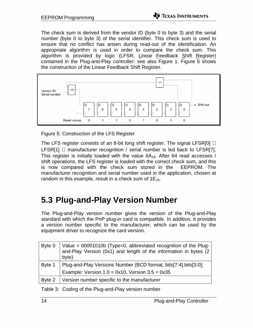
Figure 5: Construction of the LFS Register
The LFS register consists of an 8-bit long shift register. The signal LFSR[0] ⊕LFSR[1] ⊕ manufacturer recognition / serial number is led back to LFSR[7].This register is initially loaded with the value 6A16. After 64 read accesses /shift operations, the LFS register is loaded with the correct check sum, and thisis now compared with the check sum stored in the EEPROM. Themanufacturer recognition and serial number used in the application, chosen atrandom in this example, result in a check sum of 1E16.
5.3 Plug-and-Play Version NumberThe Plug-and-Play version number gives the version of the Plug-and-Playstandard with which the PnP plug-in card is compatible. In addition, it providesa version number specific to the manufacturer, which can be used by theequipment driver to recognize the card version.
Byte 0 Value = 00001010b (Type=0, abbreviated recognition of the Plug-and-Play Version (0x1) and length of the information in bytes (2byte)
Byte 1 Plug-and-Play Versions Number (BCD format, bits[7:4].bits[3:0];
Example: Version 1.0 = 0x10, Version 3.5 = 0x35
Byte 2 Version number specific to the manufacturer
Table 3: Coding of the Plug-and-Play version number

EEPROM Programming
Plug-and-Play Controller 15
Table 3 gives details of coding information. Byte 0, bit[7] gives the length of theinformation, whereby Type = 0 indicates a length of 2 to 8 byte, and Type = 1 alength of up to 64 Kbyte. The abbreviated recognition indicates that thesubsequent information identifies the Plug-and-Play version.
5.4 Identifier StringIt is possible to store a character string in the EEPROM which will appear onthe screen of the computer when the PnP plug-in card is automaticallyconfigured. Table 4 describes the format of this identification text - the"Identifier String”.
Byte 0 Value = 10000010b (Type=1, abbreviated recognition of theidentification text
Byte 1 Bits[7:0] give the lower eight bits of the string length
Byte 2 Bits[15:8] give the upper eight bits of the string length
n Bytes String in ANSI format, which describes the PC card
Table 4: Format of the identifier string
In the application presented, the character string “16550A COM Port” waschosen to describe the PnP plug-in card in more detail.
5.5 Logical Device IDThe format for identifying the logical device (Logical Device ID) is identical withthat used for serial identification (Serial Identifier). The identification serves tomake an appropriate choice of driver. In contrast to serial identification (SerialIdentifier), the identification of the logical device (Logical Device ID) does notneed to be unique: this means that the same identification may appear inconnection with another logical device. A PnP plug-in card with two COM portsmay therefore have the same identification for each COM port.
Byte 0 Value = 00010101b (Type=0, abbreviated recognition for theidentification of the logical device, length = 5
Byte 1 Logical device ID bits[7:0]
Byte 2 Logical device ID bits[15:8]
Byte 3 Logical device ID bits[23:16]
Byte 4 Logical device ID bits[31:24]
Byte 5 Bits[7:1], if set, show which configuration registers from 0x31 to0x37 are supported by the logical device.

EEPROM Programming
16 Plug-and-Play Controller
Bit[0], if set, shows that the logical device is able to participate inthe booting process.
Byte 6 Bits[7:0], if set, show which configuration registers from 0x38 to0x3F are supported by the logical device.
Table 5: Identification of the logical device
Table 5 gives individual information. In the application presented using theTL16PNP550A, byte 5 must be set to 0x02 for the identification of the logicaldevice (Logical Device ID), because this component only supports the register0x37 (I/O Range Check). For this reason, byte 6 is also not used.
5.6 Compatible Device IDWith the identification of a compatible logical device (Compatible Device ID), itis possible to give the identification of other logical devices with which the plug-in card is compatible.
Byte 0 Value = 00011100b (Type=0, abbreviated recognition of theidentification of the compatible logical device, length = 4
Byte 1 Compatible device ID bits[7:0]
Byte 2 Compatible device ID bits[15:8]
Byte 3 Compatible device ID bits[23:16]
Byte 4 Compatible device ID bits[31:24]
Table 6: Format of the identification of the compatible logical device
Table 6 shows the format of the identification of a compatible logical device(Compatible Device ID). To give an example, a card manufacturer brings out aPnP plug-in card with the Logical Device ID 0xABCD0000. At a later date, anewer PnP plug-in card is announced with the Logical Device ID 0xABCD0001,which however is 100% compatible to the older card. For this new logicaldevice, the Compatible Device ID 0xABCD0000 can be allocated. In this waythe equipment driver ID 0xABCD0001 will be loaded, if it can be found. If not,then the driver for the ID 0xABCD0000 is loaded for the logical device.
A list is available (see References in Section 11) which gives the identificationof the better known PC cards. The application described is concerned with aPlug-and-Play 16550 compatible COM port. In the list mentioned, anidentification ‘PNP0510’ is defined for this card. The corresponding CompatibleDevice ID is then known as ‘41D00501’.

EEPROM Programming
Plug-and-Play Controller 17
5.7 InterruptsThe interrupt masking indicates which interrupts must be taken into accountduring allocation. It should be possible for the corresponding interrupts to besupported by the Plug-and-Play controller. The allocation of the possible 16interrupts is undertaken by two masks with a length of 8 bit.
Byte 0 Value = 0010001xb (Type=0, abbreviated recognition of the IRQdata, length = 2 or 3
Byte 1 IRQ mask, bits[7:0]. Bit[0] = IRQ0, bit[1] = IRQ1, …
Byte 2 IRQ mask, bits[15:8]. Bit[0] = IRQ8, bit[1] = IRQ9, …
Byte 3 IRQ information. If set, each bit indicates the ability to support aspecific type of interrupt. This information contained in byte 3 isoptional. If it is not available, ISA compatibility is assumed (edge -triggering, interrupt active High).
Bit[7:4] are reserved, and must be set to 0
Bit[3] level triggering, active Low
Bit[2] level triggering, active High
Bit[1] edge triggering, active Low
Bit[0] edge triggering, active High (ISA compatible)
Table 7: Format of the Interrupt Data
Table 7 shows the format of the Interrupt data. With the circuit TL16PNP550Ait is possible to select Interrupts IRQ3 - IRQ7, IRQ9 - IRQ12 and IRQ15. In theapplication described, byte 3 of the Interrupt data was not needed, since anISA standard compatible PC card was involved.
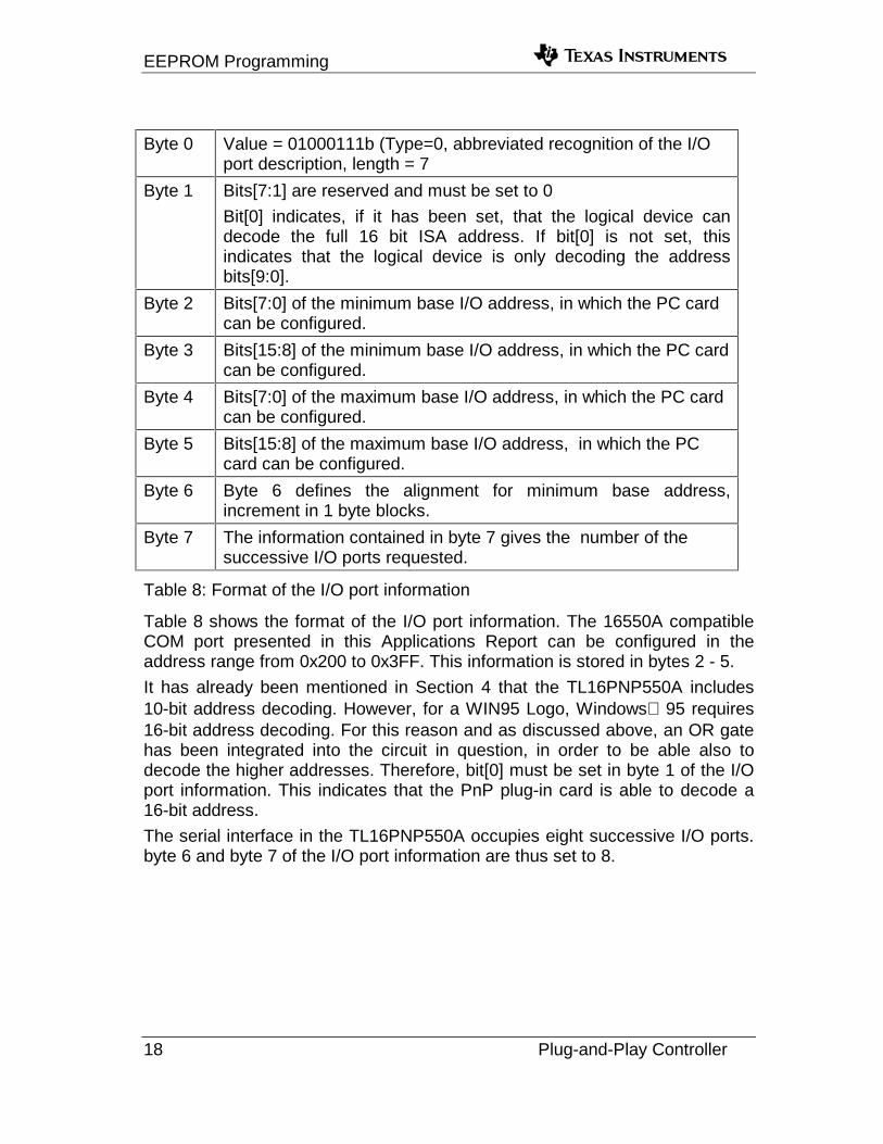
5.8 I/O PortsOn starting the computer, the I/O ports needed by a Plug-and-Play compatiblePC card are allocated. A procedure is followed in which a check is made as towhether the I/O port which has been allocated can lead to conflicts withanother PC card. For this reason the possibility is provided to allocated anaddress range to the Plug-and-Play compatible plug-in card, so that should anaddress conflict arise, a new address can be sought. This address range isdefined in the I/O port description.
EEPROM Programming
18 Plug-and-Play Controller
Byte 0 Value = 01000111b (Type=0, abbreviated recognition of the I/Oport description, length = 7
Byte 1 Bits[7:1] are reserved and must be set to 0
Bit[0] indicates, if it has been set, that the logical device candecode the full 16 bit ISA address. If bit[0] is not set, thisindicates that the logical device is only decoding the addressbits[9:0].
Byte 2 Bits[7:0] of the minimum base I/O address, in which the PC cardcan be configured.
Byte 3 Bits[15:8] of the minimum base I/O address, in which the PC cardcan be configured.
Byte 4 Bits[7:0] of the maximum base I/O address, in which the PC cardcan be configured.
Byte 5 Bits[15:8] of the maximum base I/O address, in which the PCcard can be configured.
Byte 6 Byte 6 defines the alignment for minimum base address,increment in 1 byte blocks.
Byte 7 The information contained in byte 7 gives the number of thesuccessive I/O ports requested.
Table 8: Format of the I/O port information
Table 8 shows the format of the I/O port information. The 16550A compatibleCOM port presented in this Applications Report can be configured in theaddress range from 0x200 to 0x3FF. This information is stored in bytes 2 - 5.
It has already been mentioned in Section 4 that the TL16PNP550A includes10-bit address decoding. However, for a WIN95 Logo, Windows 95 requires16-bit address decoding. For this reason and as discussed above, an OR gatehas been integrated into the circuit in question, in order to be able also todecode the higher addresses. Therefore, bit[0] must be set in byte 1 of the I/Oport information. This indicates that the PnP plug-in card is able to decode a16-bit address.
The serial interface in the TL16PNP550A occupies eight successive I/O ports.byte 6 and byte 7 of the I/O port information are thus set to 8.
EEPROM Programming
Plug-and-Play Controller 19
5.9 End MarkingThe end marking (End Tag) indicates the end of the resource data.
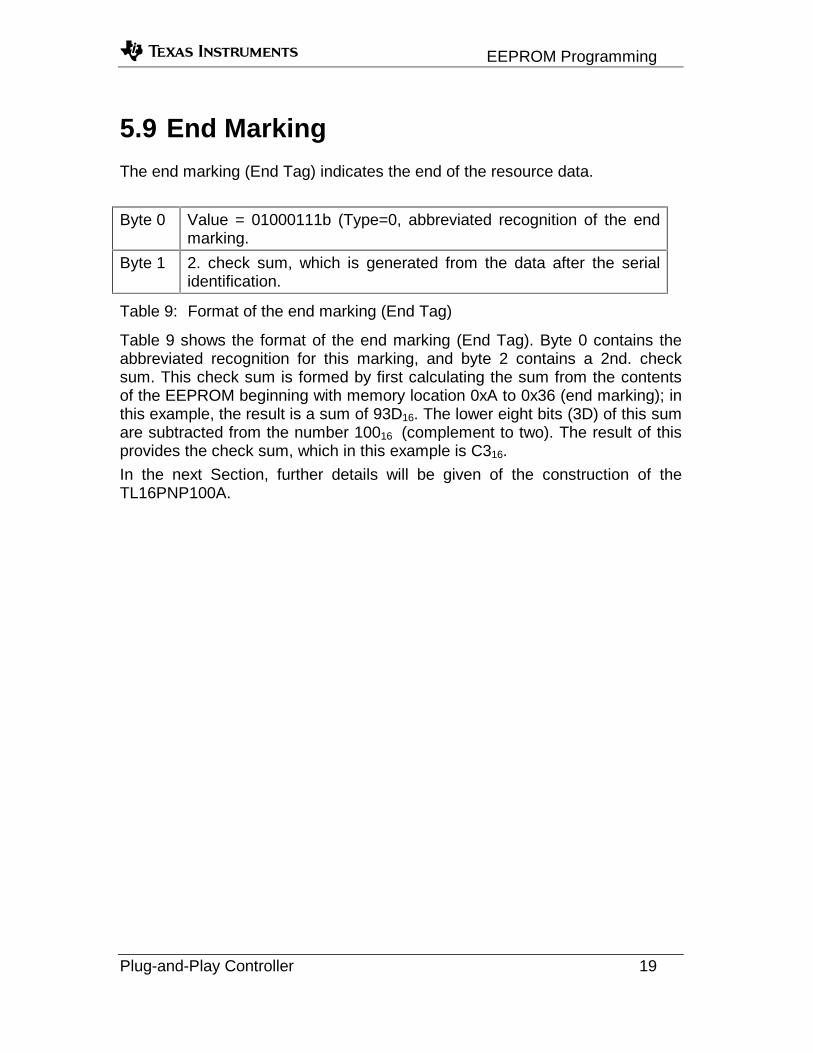
Byte 0 Value = 01000111b (Type=0, abbreviated recognition of the endmarking.
Byte 1 2. check sum, which is generated from the data after the serialidentification.
Table 9: Format of the end marking (End Tag)
Table 9 shows the format of the end marking (End Tag). Byte 0 contains theabbreviated recognition for this marking, and byte 2 contains a 2nd. checksum. This check sum is formed by first calculating the sum from the contentsof the EEPROM beginning with memory location 0xA to 0x36 (end marking); inthis example, the result is a sum of 93D16. The lower eight bits (3D) of this sumare subtracted from the number 10016 (complement to two). The result of thisprovides the check sum, which in this example is C316.
In the next Section, further details will be given of the construction of theTL16PNP100A.

TL16PNP100A
20 Plug-and-Play Controller
6. TL16PNP100AThe TL16PNP100A is a Plug-and-Play controller with which two logical devicescan be controlled. The block circuit diagram of this Plug-and-Play controller isshown in Figure 1 of this Applications Report. A typical application can be seenin Figure 6. The TL16PNP100A provides two chip-select signals CS0 andCS1 for two logical devices, which are then switched on to the ISA bus.
Figure 6: Typical application of the TL16PNP100A
The interrupt requirements of the logical devices are passed on to the Plug-and-Play controller, which in turn switches these signals on to the ISA bus. Anexternal EEPROM is also necessary with the TL16PNP100A, in order to storethe configuration data of the Plug-and-Play compatible ISA card, together withthe block sizes of the logical devices.
The next part of this Applications Report describes how the TL16PNP100A canbe used to construct a double 16550 Windows 95 compatible Plug-and-PlayCOM port.

Circuit diagram of the dual-channel COM port
Plug-and-Play Controller 21
7. Circuit diagram of the dual-channel COM port
The circuit in Figure 7 shows a dual-channel 16550 Windows 95 compatibleCOM port using the TL16PNP100A as a Plug-and-Play controller.
Figure 7: Circuit diagram of the dual-channel COM port
The hardware requirements for this interface are fairly complex, since theTL16PNP100A does not possess an integrated serial interface (UART). Theconnection of the Plug-and-Play controller to the ISA bus is however identicalto that in the circuit with the TL16PNP550A. Besides the clock generator, anEEPROM is needed in this application, and stores the configuration data ofthe two serial interfaces.
As already mentioned in Section 4, a PC card which is designated as“Windows 95 compatible” and is intended to display the WIN95 logo, must beable to decode a 16-bit I/O address. As with the TL16PNP550A, theTL16PNP100A can only decode the lower 10 bits of the ISA address bus. Forthis reason and as described in the previous application, an OR gate is neededto decode the addresses A10 - A15, and also the signal AEN. The output ofthe OR gate then switches to a Low level only if the addresses A10 - A15 andAEN are also at a Low level.
Circuit diagram of the dual-channel COM port
22 Plug-and-Play Controller
The two Chip-Select outputs CS0 and CS1 of the TL16PNP100A control theChip-Select inputs of the two circuits TL16C550C (UARTs). These are eachconnected via a bi-directional line driver SN74HCT245 to the ISA bus. Thecontrol of the line driver is performed by a PAL.
The expression for this is as follows:
G (CS I / OW I / OR)= ∨ ∧
DIR (CS I / OR)= ∨
The level conversion to the outside world is achieved by means of a V.28compatible transmitter/receiver. However, problems with the programming ofthe EEPROM arise more frequently than in the application previouslydescribed. The next Section therefore goes into more detail concerning theprogramming of the PnP plug-in card in conjunction with the TL16PNP100A.

EEPROM Programming
Plug-and-Play Controller 23
8. EEPROM ProgrammingThe Plug-and-Play controller TL16PNP100A provides an interface to theEEPROM ST93C56/66. The EEPROM contains the block sizes of the logicaldevices, and the configuration data of the Plug-and-Play ISA card. Thefollowing listing shows a programming example for a dual channel 16550AWindows 95 compatible COM port.
Address Value Description
Block Size:
0x00 0x00
0x01 0x88 Programmable block Size of the logical device
Serial Identifier:
0x02 0x43 Vendor ID byte 0
0x03 0x11 Vendor ID byte 1
0x04 0x43 Vendor ID byte 2
0x05 0x04 Vendor ID byte 3
0x06 0x00 Serial number byte 0
0x07 0x01 Serial number byte 1
0x08 0x00 Serial number byte 2
0x09 0x02 Serial number byte 3
0x0A 0x1E 1. check sum of vendor ID and serial number (byte 0x02 to byte 0x09)
Plug-and-Play Version number:
0x0B 0x0A Plug-and-Play version number descriptor
Versionsnummer
0x0C 0x10 Version in packed BCD format, example: Version 1.0
0x0D 0x01 Vendor specific version number
Identifier String:
0x0E 0x82 Identifier string descriptor
0x0F 0x13 Length byte 0 (here: 19 decimal)
0x10 0x00 Length byte 1
0x11 "2 x 16550A COM PORT" Identifier String
EEPROM Programming
24 Plug-and-Play Controller
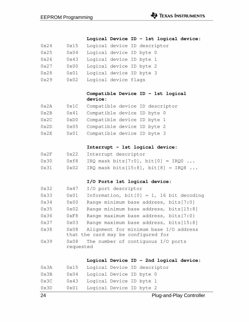
Logical Device ID - 1st logical device:
0x24 0x15 Logical device ID descriptor
0x25 0x04 Logical device ID byte 0
0x26 0x43 Logical device ID byte 1
0x27 0x00 Logical device ID byte 2
0x28 0x01 Logical device ID byte 3
0x29 0x02 Logical device flags
Compatible Device ID - 1st logical device:
0x2A 0x1C Compatible device ID descriptor
0x2B 0x41 Compatible device ID byte 0
0x2C 0xD0 Compatible device ID byte 1
0x2D 0x05 Compatible device ID byte 2
0x2E 0x01 Compatible device ID byte 3
Interrupt - 1st logical device:
0x2F 0x22 Interrupt descriptor
0x30 0xf8 IRQ mask bits[7:0], bit[0] = IRQ0 ...
0x31 0x02 IRQ mask bits[15:8], bit[8] = IRQ8 ...
I/O Ports 1st logical device:
0x32 0x47 I/O port descriptor
0x33 0x01 Information, bit[0] = 1, 16 bit decoding
0x34 0x00 Range minimum base address, bits[7:0]
0x35 0x02 Range minimum base address, bits[15:8]
0x36 0xF8 Range maximum base address, bits[7:0}
0x37 0x03 Range maximum base address, bits[15:8]
0x38 0x08 Alignment for minimum base I/O address that the card may be configured for
0x39 0x08 The number of contiguous I/O ports requested
Logical Device ID - 2nd logical device:
0x3A 0x15 Logical Device ID descriptor
0x3B 0x04 Logical Device ID byte 0
0x3C 0x43 Logical Device ID byte 1
0x3D 0x01 Logical Device ID byte 2

EEPROM Programming
Plug-and-Play Controller 25
0x3E 0x01 Logical Device ID byte 3
0x3F 0x02 Logical device flags
Compatible Device ID - 2nd logical device:
0x40 0x1C Compatible device ID descriptor
0x41 0x41 Compatible device ID byte 0
0x42 0xD0 Compatible device ID byte 1
0x43 0x05 Compatible device ID byte 2
0x44 0x01 Compatible device ID byte 3
Interrupt - 2nd logical device:
0x45 0x22 Interrupt descriptor
0x46 0xf8 IRQ mask bits[7:0], bit[0] = IRQ0 ...
0x47 0x02 IRQ mask bits[15:8], bit[8] = IRQ8 ...
I/O Ports 2nd logical device:
0x48 0x47 I/O port descriptor
0x49 0x01 Information, bit[0] = 1, 16 bit decoding
0x4A 0x00 Range minimum base address, bits[7:0]
0x4B 0x02 Range minimum base address, bits[15:8]
0x4C 0xF8 Range maximum base address, bits[7:0}
0x4D 0x03 Range maximum base address, bits[15:8}
0x4E 0x08 Alignment for minimum base I/O address that the card may be configured for
0x4F 0x08 The number of contiguous I/O ports requested
End Tag:
0x50 0x79 End Tag descriptor
0x51 0x32 2. check sum (If the check sum field is zero, the resource data is treated as if it checksummed properly. Configuration proceeds normally)
There is no difference in the configuration data when compared with theprevious application with the TL16PNP550A. The only difference is that, whenusing the TL16PNP100A, no division factor needs to be stored in theEEPROM. Instead of this, a block size for the logical devices must be stored inthe EEPROM.
EEPROM Programming
26 Plug-and-Play Controller
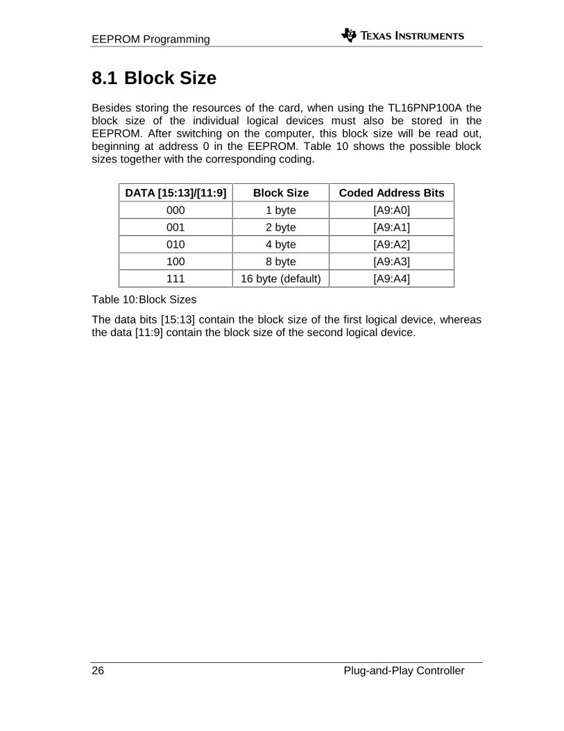
8.1 Block SizeBesides storing the resources of the card, when using the TL16PNP100A theblock size of the individual logical devices must also be stored in theEEPROM. After switching on the computer, this block size will be read out,beginning at address 0 in the EEPROM. Table 10 shows the possible blocksizes together with the corresponding coding.
DATA [15:13]/[11:9] Block Size Coded Address Bits
000 1 byte [A9:A0]
001 2 byte [A9:A1]
010 4 byte [A9:A2]
100 8 byte [A9:A3]
111 16 byte (default) [A9:A4]
Table 10:Block Sizes
The data bits [15:13] contain the block size of the first logical device, whereasthe data [11:9] contain the block size of the second logical device.

References
Plug-and-Play Controller 27
9. ReferencesTexas Instruments, Data Sheet TL16PNP550A SLLS190A
Texas Instruments, Data Sheet TL16PNP100A SLLS200A
Texas Instruments, Data Book Data Transmission Circuits SLLD001A
Texas Instruments, Data Book Data Transmission Circuits SLLD003
Texas Instruments, Data Sheet SN74HCT245 SCLS020B
Texas Instruments, Data Sheet TIBPAL16L8 SRPS006D
Intel Corporation / Microsoft Corporation, Plug-and-Play ISA Specification,Version 1.0a, May 5, 1994
Microsoft, PC card identification,http://www.microsoft.com/hwdev/download/devids.txt