Deterministic photon-emitter coupling in chiral photonic ...
5
Deterministic photon–emitter coupling in chiral photonic circuits Immo Söllner 1 * , Sahand Mahmoodian 1 , Sofie Lindskov Hansen 1 , Leonardo Midolo 1 , Alisa Javadi 1 , Gabija Kiršanskė 1 , Tommaso Pregnolato 1 , Haitham El-Ella 1 , Eun Hye Lee 2 , Jin Dong Song 2 , Søren Stobbe 1 and Peter Lodahl 1 * Engineering photon emission and scattering is central to modern photonics applications ranging from light harvesting to quantum-information processing. To this end, nanophotonic waveguides are well suited as they confine photons to a one- dimensional geometry and thereby increase the light–matter interaction. In a regular waveguide, a quantum emitter interacts equally with photons in either of the two propagation direc- tions. This symmetry is violated in nanophotonic structures in which non-transversal local electric-field components imply that photon emission 1,2 and scattering 3 may become direc- tional. Here we show that the helicity of the optical transition of a quantum emitter determines the direction of single- photon emission in a specially engineered photonic-crystal waveguide. We observe single-photon emission into the wave- guide with a directionality that exceeds 90% under conditions in which practically all the emitted photons are coupled to the waveguide. The chiral light–matter interaction enables determi- nistic and highly directional photon emission for experimentally achievable on-chip non-reciprocal photonic elements. These may serve as key building blocks for single-photon optical diodes, transistors 4 and deterministic quantum gates 5 . Furthermore, chiral photonic circuits allow the dissipative prep- aration of entangled states of multiple emitters 6 for experimen- tally achievable parameters 7 , may lead to novel topological photon states 8,9 and could be applied for directional steering of light 10–13 . Truly 1D photon/emitter interfaces are desirable for a range of applications in photonic quantum-information processing 14 . To this end, photonic-crystal waveguides constitute an ideal platform that features on-chip integration with the ability to engineer the light–matter coupling. Recent experiments achieved a coupling effi- ciency for a single quantum dot (QD) to a photonic-crystal wave- guide in excess of 98%, which thus constitutes a deterministic 1D photon/emitter interface 15 . Standard photonic-crystal waveguides are mirror symmetric around the centre of the waveguide, and all modes consequently have odd/even symmetry under a reflection in a vertical centre plane. The electric-field maxima are positioned in the centre plane for a standard photonic-crystal waveguide and, as a consequence, the mode polarization is predominantly linear at the positions where the light intensity is high 14,15 (see the Supplementary Information for more details). Therefore, breaking this symmetry is required to engineer modes that are circularly polarized at the field maxima. An ideal way to break the reflection symmetry is by shifting one side of the waveguide by half a lattice constant, which is referred to as a glide-plane waveguide (GPW) (see the Supplementary Information for further descriptions of the structure). In a GPW, a QD with a circularly polarized transition dipole emits preferentially in a single direction. The direction is determined by the helicity (see Fig. 1a), and the exact branching ratio between the two emission directions depends on the position of the QD. The two figures-of-merit for chiral single-photon emis- sion are displayed in Fig. 1b,c. They are the fraction of photons emitted into the waveguide that propagates in a desired direction (F dir ) and the overall probability that an emitted photon from the QD is channelled into the correct direction (β dir ). The GPW is engineered to increase the β factor and features β dir = 98% (see Fig. 1c), which enables the deterministic interfacing of single emit- ters and single photons. An ideal directional photon/emitter inter- face corresponds to β dir 1, which probably can be achieved by further engineering of the GPW. We emphasize the robustness of the directional coupling, because the GPW is designed to have a highly directional coupling within a large region of each unit cell of the photonic-crystal waveguide. The present work reports on the observation of highly directional emission at the single- photon level by efficiently coupling a single QD to a GPW. We show that this is the basic operational principle required to construct non-reciprocal elements based on chiral photonic circuits. Figure 1d displays a scanning electron microscope (SEM) image of our photonic waveguide and illustrates the directional coupling. Single self-assembled QDs in the GPW are excited optically and two non-degenerate circularly polarized exciton states, | +〉 and | -〉 (see Fig. 1a), are formed by applying a strong magnetic field (B z ) in the QD growth direction 16 . By non-resonant optical excitation, a stat- istical mixture of the two exciton states is prepared that can decay to the ground state via Δm = ±1 dipole transitions that emit σ ± polarized photons. These QD transitions are used to demonstrate chiral photon emission. The origin of the chiral interaction can be under- stood as follows: from time-reversal symmetry, the electric fields, E, of counter-propagating modes with wave vectors k and -k satisfy E -k (r)= E * k (r), that is, for a mode with an in-plane circular polariz- ation at position r, the counter-propagating mode has the orthogonal circular polarization. As a circularly polarized emitter only couples to the mode that has the same circular polarization as the dipole transition, this leads to unidirectional emission. An important advantage of photonic crystals is that they allow the interaction between light and matter to be tailored. In a GPW, the chirality is engineered by the structural parameters and depends on the magnitude of the projection of the local electric field onto the QD transition dipole moment (see Fig. 1b,c). The experimental proof of directional emission is obtained by collecting single photons emitted from the QDs by two separate outcoupling gratings at each end of the GPW (see Fig. 1d). We extract the direc- tionality factor F dir by comparing the intensity of one circular dipole to the orthogonal dipole by collecting the intensity from the same 1 Niels Bohr Institute, University of Copenhagen, Blegdamsvej 17, Copenhagen DK-2100, Denmark. 2 Center for Opto-Electronic Convergence Systems, Korea Institute of Science and Technology, Seoul 136-791, Korea. *e-mail: [email protected]; [email protected] LETTERS PUBLISHED ONLINE: 27 JULY 2015 | DOI: 10.1038/NNANO.2015.159 NATURE NANOTECHNOLOGY | VOL 10 | SEPTEMBER 2015 | www.nature.com/naturenanotechnology 775 © 2015 Macmillan Publishers Limited. All rights reserved
Transcript of Deterministic photon-emitter coupling in chiral photonic ...

Deterministic photon–emitter couplingin chiral photonic circuitsImmo Söllner1*, Sahand Mahmoodian1, Sofie Lindskov Hansen1, Leonardo Midolo1, Alisa Javadi1,Gabija Kiršanskė1, Tommaso Pregnolato1, Haitham El-Ella1, Eun Hye Lee2, Jin Dong Song2,Søren Stobbe1 and Peter Lodahl1*
Engineering photon emission and scattering is central tomodern photonics applications ranging from light harvestingto quantum-information processing. To this end, nanophotonicwaveguides are well suited as they confine photons to a one-dimensional geometry and thereby increase the light–matterinteraction. In a regular waveguide, a quantum emitter interactsequally with photons in either of the two propagation direc-tions. This symmetry is violated in nanophotonic structures inwhich non-transversal local electric-field components implythat photon emission1,2 and scattering3 may become direc-tional. Here we show that the helicity of the optical transitionof a quantum emitter determines the direction of single-photon emission in a specially engineered photonic-crystalwaveguide. We observe single-photon emission into the wave-guide with a directionality that exceeds 90% under conditionsin which practically all the emitted photons are coupled to thewaveguide. The chiral light–matter interaction enables determi-nistic and highly directional photon emission for experimentallyachievable on-chip non-reciprocal photonic elements. Thesemay serve as key building blocks for single-photon opticaldiodes, transistors4 and deterministic quantum gates5.Furthermore, chiral photonic circuits allow the dissipative prep-aration of entangled states of multiple emitters6 for experimen-tally achievable parameters7, may lead to novel topologicalphoton states8,9 and could be applied for directional steeringof light10–13.
Truly 1D photon/emitter interfaces are desirable for a range ofapplications in photonic quantum-information processing14. Tothis end, photonic-crystal waveguides constitute an ideal platformthat features on-chip integration with the ability to engineer thelight–matter coupling. Recent experiments achieved a coupling effi-ciency for a single quantum dot (QD) to a photonic-crystal wave-guide in excess of 98%, which thus constitutes a deterministic 1Dphoton/emitter interface15. Standard photonic-crystal waveguidesare mirror symmetric around the centre of the waveguide, and allmodes consequently have odd/even symmetry under a reflectionin a vertical centre plane. The electric-field maxima are positionedin the centre plane for a standard photonic-crystal waveguide and,as a consequence, the mode polarization is predominantly linearat the positions where the light intensity is high14,15 (see theSupplementary Information for more details). Therefore, breakingthis symmetry is required to engineer modes that are circularlypolarized at the field maxima. An ideal way to break the reflectionsymmetry is by shifting one side of the waveguide by half a latticeconstant, which is referred to as a glide-plane waveguide (GPW)(see the Supplementary Information for further descriptions ofthe structure). In a GPW, a QD with a circularly polarized transition
dipole emits preferentially in a single direction. The direction isdetermined by the helicity (see Fig. 1a), and the exact branchingratio between the two emission directions depends on the positionof the QD. The two figures-of-merit for chiral single-photon emis-sion are displayed in Fig. 1b,c. They are the fraction of photonsemitted into the waveguide that propagates in a desired direction(Fdir) and the overall probability that an emitted photon from theQD is channelled into the correct direction (βdir). The GPW isengineered to increase the β factor and features βdir = 98% (seeFig. 1c), which enables the deterministic interfacing of single emit-ters and single photons. An ideal directional photon/emitter inter-face corresponds to βdir�1, which probably can be achieved byfurther engineering of the GPW. We emphasize the robustness ofthe directional coupling, because the GPW is designed to have ahighly directional coupling within a large region of each unit cellof the photonic-crystal waveguide. The present work reports onthe observation of highly directional emission at the single-photon level by efficiently coupling a single QD to a GPW. Weshow that this is the basic operational principle required to constructnon-reciprocal elements based on chiral photonic circuits.
Figure 1d displays a scanning electron microscope (SEM) image ofour photonic waveguide and illustrates the directional coupling.Single self-assembled QDs in the GPW are excited optically andtwo non-degenerate circularly polarized exciton states, |+⟩ and |−⟩(see Fig. 1a), are formed by applying a strong magnetic field (Bz) inthe QD growth direction16. By non-resonant optical excitation, a stat-istical mixture of the two exciton states is prepared that can decay tothe ground state viaΔm = ±1 dipole transitions that emit σ± polarizedphotons. These QD transitions are used to demonstrate chiralphoton emission. The origin of the chiral interaction can be under-stood as follows: from time-reversal symmetry, the electric fields, E,of counter-propagating modes with wave vectors k and −k satisfyE−k(r) = E*
k(r), that is, for a mode with an in-plane circular polariz-ation at position r, the counter-propagating mode has the orthogonalcircular polarization. As a circularly polarized emitter only couplesto the mode that has the same circular polarization as the dipoletransition, this leads to unidirectional emission.
An important advantage of photonic crystals is that they allowthe interaction between light and matter to be tailored. In a GPW,the chirality is engineered by the structural parameters anddepends on the magnitude of the projection of the local electricfield onto the QD transition dipole moment (see Fig. 1b,c). Theexperimental proof of directional emission is obtained by collectingsingle photons emitted from the QDs by two separate outcouplinggratings at each end of the GPW (see Fig. 1d). We extract the direc-tionality factor Fdir by comparing the intensity of one circular dipoleto the orthogonal dipole by collecting the intensity from the same
1Niels Bohr Institute, University of Copenhagen, Blegdamsvej 17, Copenhagen DK-2100, Denmark. 2Center for Opto-Electronic Convergence Systems, KoreaInstitute of Science and Technology, Seoul 136-791, Korea. *e-mail: [email protected]; [email protected]
LETTERSPUBLISHED ONLINE: 27 JULY 2015 | DOI: 10.1038/NNANO.2015.159
NATURE NANOTECHNOLOGY | VOL 10 | SEPTEMBER 2015 | www.nature.com/naturenanotechnology 775
© 2015 Macmillan Publishers Limited. All rights reserved

waveguide ends, which makes the method insensitive to potentiallydifferent outcoupling efficiencies at the two ends (see theSupplementary Information). By spectrally resolving the emission,single QD lines are selected and photon correlation measurementsare employed to identify separate QDs and quantify the single-photon nature of the emission.
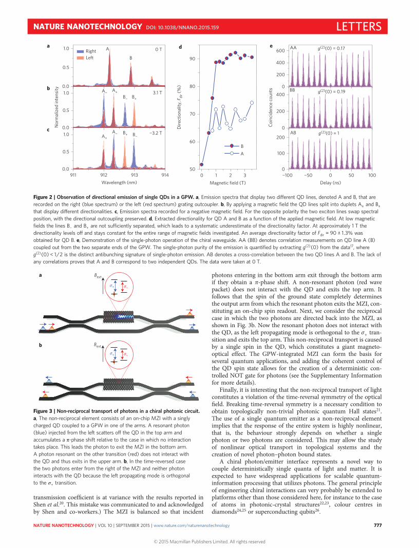
The directionality of the photon emission is extracted from theemission spectra measured for different applied magnetic fieldstrengths (see Fig. 2a–c) and two QD lines (A and B) are studiedin detail. Without a magnetic field, the spectra recorded from thetwo ends of the GPW are almost identical. By increasing the mag-netic field, the individual QD lines split into pairs that correspondto the two circularly polarized transitions. Highly directional emis-sion is evident for the peaks labelled B+ and B−. Furthermore,Fig. 2b,c show that the two transitions maintain their directionalitywhen changing the polarity of the magnetic field, which swaps thespectral position of orthogonally polarized emission lines. Thisdemonstrates explicitly that the directionality is related to the heli-city of the dipole transition.
Figure 2d shows a plot of the directionality of the two QD lines asa function of the applied magnetic field strength. At low magneticfields the emission lines are not separated clearly, which leads toa systematic underestimation of the directionality factor. Atapproximately 1 T the directionality levels off and we extractFdir = 90 ± 1.3% for QD B by averaging over the plateau region inFig. 2d. The lower directionality of QD A stems from the spatialvariation within the unit cell of the GPW (see Fig. 1b). The extracteddirectionality constitutes a lower bound of the actual value becauseof the presence of weak emission from transitions other than theinvestigated QD, which is a result of the non-resonant excitationmethod applied in the experiment. In addition, the presence ofresidual reflections at the outcoupling gratings further limits the
experimentally extracted value. Consequently, the actual direction-ality for the single QD transition is likely to approach unity, inaccordance with theory (Fig. 1b). The single-photon nature of theemission can be proved through correlation measurements (seeFig. 2e). A pronounced antibunching is observed for peaks A and B,which illustrates that high-purity single-photon emission isobserved. Furthermore, the absence of correlations in the cross-cor-relation measurement between A and B shows that the two peaksoriginate from two independent QDs.
A major asset of the photonic-crystal waveguide platform is thatthe light–matter interaction can be controlled to such a degree thatthe photon/emitter interface becomes deterministic14, as is quanti-fied by the β factor. In time-resolved measurements, we recordeda decay rate of 0.80 ± 0.02 ns−1 for QD B. This restricts the possiblespatial position of the QD as well as its spectral position relative tothe photonic waveguide bands of the GPW. From numericalcalculations, we estimate an upper bound on the rate at which theQD leaks to non-guided modes, and also, by accounting for thecontribution from intrinsic non-radiative decay processes of theQD, we arrive at β≳ 90%. The detailed measurements of the βfactor in standard photonic-crystal waveguides are presented inArcari et al.15.
Having demonstrated the basic operational principle of determi-nistic chiral photon emission, this functionality can be exploited forthe construction of non-reciprocal photonic elements, such assingle-photon diodes and circulators. The architecture is based ona QD coupled to a GPW, which is placed in one arm of a Mach–Zehnder interferometer (MZI) (see Fig. 3a). We consider the scat-tering by a singly charged QD initially prepared in the spin-upstate18. A resonant narrow-band single photon (blue wave packet)scatters off the QD transition and obtains a π-phase shift19 (seethe Supplementary Information for the calculations). (The acquired
a b
|+⟩
|+⟩
|−⟩
|−⟩
|g⟩
|g⟩
c1.0
βdirFdir
0.9
0.8
0.7
0.6
0.5
−0.5 0.50.0
x/a
−0.5
−7
−1
1
0
−2
2
0
0.50.0
0 70
Max.|E|2
|E|2
0
Max.
−7 0 7
x/ax/a
y/a
y/a
−2
2
0y/a
0.4
d
5 µm
1.0
0.9
0.8
0.7
0.6
0.5
σ−
σ+
σ+
σ−
Figure 1 | Operational principle of chiral single-photon emission in a waveguide. a, Left: QD-level scheme in the presence of a magnetic field in the growthdirections that features two circularly polarized exciton transitions σ± with a splitting controlled by the magnetic field. Right: calculated directional emissionpatterns of σ+ and σ− polarized dipole emitters in GPWs. The positions of the dipoles are indicated by the crosses in b and c. b,c, Directionality (b) anddirectional β factor (c) as a function of position for the GPW mode studied in the experiments. Here, a is the lattice constant of the photonic crystal. d, SEMimage of the GPW. A QD is excited in the centre of the structure (green area) and photons are collected from the outcoupling gratings at each side of theGPW (red and blue areas). The zoom-ins show the structure of the photonic-crystal lattice that consists of a GPW section (left image) and a standardphotonic-crystal waveguide section (right image). The waveguide gradually changes from a glide-plane lattice to a standard lattice to obtain an efficientoutcoupling of photons (for the details, see the Supplementary Information).
LETTERS NATURE NANOTECHNOLOGY DOI: 10.1038/NNANO.2015.159
NATURE NANOTECHNOLOGY | VOL 10 | SEPTEMBER 2015 | www.nature.com/naturenanotechnology776
© 2015 Macmillan Publishers Limited. All rights reserved
transmission coefficient is at variance with the results reported inShen et al.20. This mistake was communicated to and acknowledgedby Shen and co-workers.) The MZI is balanced so that incident
photons entering in the bottom arm exit through the bottom armif they obtain a π-phase shift. A non-resonant photon (red wavepacket) does not interact with the QD and exits the top arm. Itfollows that the spin of the ground state completely determinesthe output arm from which the resonant photon exits the MZI, con-stituting an on-chip spin readout. Next, we consider the reciprocalcase in which the two photons are directed back into the MZI, asshown in Fig. 3b. Now the resonant photon does not interact withthe QD, as the left propagating mode is orthogonal to the σ+ tran-sition and exits the top arm. This non-reciprocal transport is causedby a single spin in the QD, which constitutes a giant magneto-optical effect. The GPW-integrated MZI can form the basis forseveral quantum applications, and adding the coherent control ofthe QD spin state allows for the creation of a deterministic con-trolled NOT gate for photons (see the Supplementary Informationfor more details).
Finally, it is interesting that the non-reciprocal transport of lightconstitutes a violation of the time-reversal symmetry of the opticalfield. Breaking time-reversal symmetry is a necessary condition toobtain topologically non-trivial photonic quantum Hall states21.The use of a single quantum emitter as a non-reciprocal elementimplies that the response of the entire system is highly nonlinear,that is, the behaviour strongly depends on whether a singlephoton or two photons are considered. This may allow the studyof nonlinear optical transport in topological systems and thecreation of novel photon–photon bound states.
A chiral photon/emitter interface represents a novel way tocouple deterministically single quanta of light and matter. It isexpected to have widespread applications for scalable quantum-information processing that utilizes photons. The general principleof engineering chiral interactions can very probably be extended toplatforms other than those considered here, for instance to the caseof atoms in photonic-crystal structures22,23, colour centres indiamonds24,25 or superconducting qubits26.
a Bext
Bext
σ+
σ+ σ−
σ−
b
Figure 3 | Non-reciprocal transport of photons in a chiral photonic circuit.a, The non-reciprocal element consists of an on-chip MZI with a singlycharged QD coupled to a GPW in one of the arms. A resonant photon(blue) injected from the left scatters off the QD in the top arm andaccumulates a π-phase shift relative to the case in which no interactiontakes place. This leads the photon to exit the MZI in the bottom arm.A photon resonant on the other transition (red) does not interact withthe QD and thus exits in the upper arm. b, In the time-reversed casethe two photons enter from the right of the MZI and neither photoninteracts with the QD because the left propagating mode is orthogonalto the σ+ transition.
0.0
0.5
1.0
0 1 2 350
60
70
80
90
911 912 913 9140.0
0.5
1.00.0
0.5
1.00
200
400
600
0
200
400
−100 −50 0 50 1000
100
200
B
0 TRightLeft
A
BA
Delay (ns)
Coi
ncid
ence
cou
nts
3.1 T
d
Dire
ctio
nalit
y, F
dir (
%)
Magnetic field (T)Wavelength (nm)
B− B+
−3.2 T
A− A+
Nor
mal
ized
inte
nsity
a
b
c
e
B−B+
A−A+
g(2)(0) = 0.19
g(2)(0) = 0.17
g(2)(0) = 1AB
BB
AA
Figure 2 | Observation of directional emission of single QDs in a GPW. a, Emission spectra that display two different QD lines, denoted A and B, that arerecorded on the right (blue spectrum) or the left (red spectrum) grating outcoupler. b, By applying a magnetic field the QD lines split into duplets A± and B±that display different directionalities. c, Emission spectra recorded for a negative magnetic field. For the opposite polarity the two exciton lines swap spectralposition, with the directional outcoupling preserved. d, Extracted directionality for QD A and B as a function of the applied magnetic field. At low magneticfields the lines B− and B+ are not sufficiently separated, which leads to a systematic underestimate of the directionality factor. At approximately 1 T thedirectionality levels off and stays constant for the entire range of magnetic fields investigated. An average directionality factor of Fdir = 90 ± 1.3% wasobtained for QD B. e, Demonstration of the single-photon operation of the chiral waveguide. AA (BB) denotes correlation measurements on QD line A (B)coupled out from the two separate ends of the GPW. The single-photon purity of the emission is quantified by extracting g(2)(0) from the data17, whereg(2)(0) < 1/2 is the distinct antibunching signature of single-photon emission. AB denotes a cross-correlation between the two QD lines A and B. The lack ofany correlations proves that A and B correspond to two independent QDs. The data were taken at 0 T.
NATURE NANOTECHNOLOGY DOI: 10.1038/NNANO.2015.159 LETTERS
NATURE NANOTECHNOLOGY | VOL 10 | SEPTEMBER 2015 | www.nature.com/naturenanotechnology 777
© 2015 Macmillan Publishers Limited. All rights reserved

MethodsMethods and any associated references are available in the onlineversion of the paper.
Received 7 December 2014; accepted 22 June 2015;published online 27 July 2015
References1. Mitsch, R., Sayrin, C., Albrecht, B., Schneeweiss, P. & Rauschenbeutel, A.
Quantum state-controlled directional spontaneous emission of photons into ananophotonic waveguide. Nature Commun. 5, 5713 (2014).
2. Luxmoore, I. J. et al. Interfacing spins in an InGaAs quantum dot to asemiconductor waveguide circuit using emitted photons. Phys. Rev. Lett.110, 037402 (2013).
3. Junge, C., O’Shea, D., Volz, J. & Rauschenbeutel, A. Strong coupling betweensingle atoms and nontransversal photons. Phys. Rev. Lett. 110, 213604 (2013).
4. Chang, D. E., Sørensen, A. S., Demler, E. A. & Lukin, M. D. A single-photontransistor using nanoscale surface plasmons. Nature Phys. 3, 807–812 (2007).
5. Duan, L. M. & Kimble, H. J. Scalable photonic quantum computation throughcavity-assisted interactions. Phys. Rev. Lett. 92, 127902 (2004).
6. Stannigel, K., Rabl, P. & Zoller, P. Driven-dissipative preparation of entangledstates in cascaded quantum-optical networks. New J. Phys. 14, 063014 (2012).
7. Ramos, T., Pichler, H., Daley, A. J. & Zoller, P. Quantum spin dimers fromchiral dissipation in cold-atom chains. Phys. Rev. Lett. 113, 237203 (2014).
8. Hafezi, M., Demler, E. A., Lukin, M. D. & Taylor, J. M. Robust optical delaylines with topological protection. Nature Phys. 7, 907–912 (2010).
9. Kraus, Y. E., Lahini, Y., Ringel, Z., Verbin, M. & Zilberberg, O. Topological statesand adiabatic pumping in quasicrystals. Phys. Rev. Lett. 109, 106402 (2012).
10. Rodriguez-Fortuño, F. J. et al. Near-field interference for the unidirectionalexcitation of electromagnetic guided modes. Science 340, 328–330 (2013).
11. Petersen, J., Volz, J. & Rauschenbeutel, A. Chiral nanophotonic waveguideinterface based on spin–orbit interaction of light. Science 346, 67–71 (2014).
12. Neugebauer, M., Bauer, T., Banzer, P. & Leuchs, G. Polarization tailoredlight driven directional optical nanobeacon. Nano Lett. 14, 2546–2551 (2014).
13. le Feber, B., Rotenberg, N. & Kuipers, L. Nanophotonic control of circulardipole emission. Nature Commun. 6, 6695 (2015).
14. Lodahl, P., Mahmoodian, S. & Stobbe, S. Interfacing single photons andsingle quantum dots with photonic nanostructures. Rev. Mod. Phys. 87,347–400 (2015).
15. Arcari, M. et al. Near-unity coupling efficiency of a quantum emitter to aphotonic crystal waveguide. Phys. Rev. Lett. 113, 093603 (2014).
16. Bayer, M. et al. Fine structure of neutral and charged excitons in self-assembledIn(Ga)As/(Al)GaAs quantum dots. Phys. Rev. B 65, 195315 (2002).
17. Santori, C., Fattal, D. & Yamamoto, Y. Single-Photon Devices and Applications(John Wiley & Sons, Inc., 2010).
18. Yilmaz, S. T., Fallahi, P. & Imamoglu, A. Quantum-dot-spin single-photoninterface. Phys. Rev. Lett. 105, 033601 (2010).
19. Fan, S., Kocabaş, Ş. E. & Shen, J.-T. Input–output formalism for few-photontransport in one-dimensional nanophotonic waveguides coupled to a qubit.Phys. Rev. A 82, 063821 (2010).
20. Shen, Y., Bradford, M. & Shen, J.-T. Single-photon diode by exploiting thephoton polarization in a waveguide. Phys. Rev. Lett. 107, 173902 (2011).
21. Lu, L., Joannopoulos, J. D. & Soljačić, M. Topological photonics. Nature Photon.8, 821–829 (2014).
22. Tiecke, T. G. et al. Nanophotonic quantum phase switch with a single atom.Nature 508, 241–244 (2014).
23. Goban, A. et al. Atom–light interactions in photonic crystals. Nature Commun.5, 4808 (2014).
24. Riedrich-Möller, J. et al. Deterministic coupling of a single silicon-vacancy colorcenter to a photonic crystal cavity in diamond. Nano Lett. 14, 5281–5287 (2014).
25. Li, L. et al. Coherent spin control of a nanocavity-enhanced qubit in diamond.Nature Commun. 6, 6173 (2015).
26. Hoi, I.-C. et al. Generation of nonclassical microwave states using an artificialatom in 1D open space. Phys. Rev. Lett. 108, 263601 (2012).
AcknowledgementsWe thank A. Sørensen and D.Witthaut for valuable discussions and gratefully acknowledgefinancial support from the Villum Foundation, the Carlsberg Foundation, the DanishCouncil for Independent Research (Natural Sciences and Technology and ProductionSciences), and the European Research Council (ERC Consolidator GrantALLQUANTUM). E.H.L. and J.D.S. acknowledge support from the Global Research Laband the Flagship Program (Korea Institute of Science and Technology).
Author contributionsI.S. and S.M. designed the experiment and analysed the data. S.M. and A.J. performed thenumerical simulations. I.S. and S.L.H. carried out the experiments. L.M., G.K., T.P. andH.E.fabricated the sample. E.H.L. and J.D.S. grew the semiconductor material. P.L. and S.S.supervised the project. P.L., S.S., S.M. and I.S. wrote the manuscript with input from allthe authors.
Additional informationSupplementary information is available in the online version of the paper. Reprints andpermissions information is available online at www.nature.com/reprints. Correspondence andrequests for materials should be addressed to I.S. and P.L.
Competing financial interestsThe authors declare no competing financial interests.
LETTERS NATURE NANOTECHNOLOGY DOI: 10.1038/NNANO.2015.159
NATURE NANOTECHNOLOGY | VOL 10 | SEPTEMBER 2015 | www.nature.com/naturenanotechnology778
© 2015 Macmillan Publishers Limited. All rights reserved

MethodsSample. The sample was grown by molecular beam epitaxy on an undoped (100)GaAs substrate. A 160 nm thick GaAs membrane was grown on a 1.42 µm thickAl0.75Ga0.25As sacrificial layer. The membrane contained a single layer of low-density self-assembled In(Ga)As QDs, and emitted around 920 nm at 10 K(density ≃ 50 μm−2). The photonic nanostructures were patterned by electron-beamlithography at 100 keV on a 500 nm thick electron beam resist (ZEP 520A) andaligned to the [011] or [0–11] directions of the GaAs substrate. The photonic-crystalholes were etched by an inductively coupled plasma in a BCl3/Cl2/Ar chemistry at0 °C. The remaining photoresist was stripped using hot N-methyl-2-pyrrolidone andthe membranes were subsequently released in a wet-etching step, which removed theAlGaAs sacrificial layer using a hydrofluoric acid solution (10% w/w).
Experiment. The measurements were performed in a helium-bath cryostatoperating at 4.2 K. The samples were mounted on a stack of piezoelectric
nanopositioning stages that allowed for a precise positioning of the sample withrespect to the objective. A superconducting coil was able to generate magnetic fieldsup to 9 T and surrounded the stage and sample such that the generated field pointedalong the QD growth direction. The QDs were optically pumped by a Ti:sapphirelaser at an emission wavelength of 842 nm. The laser was operated in thecontinuous-wave mode for the spectral measurements and in the pulsed mode(3 ps pulses at a repetition rate of 76 MHz) for lifetime and correlationmeasurements. Both excitation and collection were performed through the samemicroscope objective (numerical aperture, 0.65). The excitation beam was moved tothe centre of the waveguide and the emission was collected from both gratings atthe same time. The emission from the two gratings was coupled into separatesingle-mode polarization-maintaining fibres that each led to their own spectrometerset-up (1,200 grooves mm–1 grating), where avalanche photodiodes were used fortime-resolved measurements, and a charge-coupled device was used to recordthe spectra.
NATURE NANOTECHNOLOGY DOI: 10.1038/NNANO.2015.159 LETTERS
NATURE NANOTECHNOLOGY | www.nature.com/naturenanotechnology
© 2015 Macmillan Publishers Limited. All rights reserved