
Detection of lateral composition modulation in a …/67531/metadc683261/m2/1/high...Detection of...
6
s&vo 4 3- 0 5 S& @4F*H0&3/=47 Detection of lateral composition modulation in a (InAs)n/(GaAs)n short period superlattice on InP by magnetoexciton spectroscopy E. D. Jonesa, J. Mirecki-Millunchicka, D. Follstaedta,M. Haficha, S. Leea, J. Renoa, R. Twestena, Y. Zhangb, and A. Mascarenhasb a) Sandia National Laboratories, Albuquerque, NM 87185-0601, USA b) National Energy Renewable Laboratory, Golden, CO 80401 ABSTRACT An experimental signature for detecting spontaneous lateral compositionmodulation in a (InAs),/(GaAS), short period superlattice on a InP substrate based on magnetoexciton spectroscopy is presented. We find by aligning the magnetic field in three crystallographic directions, one parallel to and the other two perpendicular to the composition modulation direction, that the magnetoexciton shifts are anisotropic and are a good indicator for the presence of composition modulation 2. INTRODUCTION Low-dimensional structures, such as quantum wires and dots, have the potential to revolutionize microelectronic and photonic devices. These types of structures are expected to have lower laser-threshold currents, wider modulation bandwidths, better temperature stability, etc. However, they have been problematic to manufacture due to limitations in post-growth pro- cessing. Alternatively, self-assembled structures that are arranged in quantum-sizeconfigurations during growth can be used to obtain high densities of quantum wires and dots. For example, deposition of short period superlattices (SPS) of IU-V alloys have resulted in lateral composition modulation which produces quantum wire structures. The phenomenon of spontaneous compo- sition modulation in semiconductorshas received attention in the literature where recently, an up-to-date summary of theoretical considerations,growth conditions, microscopy studies, and device applicationswas published as a conference proceedings.* To date, the principle experimental verifications for composition modulation have consisted of transmission electron microscopy, * optical absorption? and polarized photoluminescence techniques? Recently, x-ray reciprocal space analysis has also proven to be a valuable diagnostic tool for the detection and measurement of compositionmodulationP ' Transmission electron microscopy (TEM) is a powerful diagnostic and in m+y instances is the definitive measure- ment for microstructural analysis. However, because of sample preparation requirements, the TEM measurement can be labor intensive. As stated above, the application of x-ray reciprocal space analysis (W) for studying composition modulation is relatively new and offers a rapid tool for characterization of not only composition modulation, but also for measuring lattice constants, strain parameters, etc?.' Polarized photoluminescence techniques relies on crystal-field splitting of the valence- bands caused by the lowering of the zincblende cubic-symmetry by composition modulation? However, besides composition modulation, there are other situations which also lead to reducing the crystal-field symmetry and two are (1) strained epilayers due to lattice mismatch between the substrate and the deposited film giving rise to a energy splitting of the valence-band states, ' and (2) spontaneous ordering effects such as observed for MOCVD-grown InGaAs epilayers on InP which result in a CuPt-type crystal structure. 6 In this paper we report a new diagnostic tool using an old technique, magnetoexciton spectroscopy, for the detection of spontaneous lateral composition modulation. Here the magnetoexciton shifts are studied for three orientations of the mag- netic field with respect to the direction of the composition modulation, giving a relatively fast and unambiguous determination for the presence of composition modulation. The structure used to demonstratethe utility ofmagnetoexciton spectroscopy is an (InAs),/(GaAs), SPS on a InP substrate that has spontaneously formed a lateral superlatticd, perpendicular to the growth direc- tion. The microstructure was confumed by cross-sectional TEM, high resolution electron microscopy, and also low-temperature polarized photoluminescence spectroscopy.
Transcript of Detection of lateral composition modulation in a …/67531/metadc683261/m2/1/high...Detection of...

s&vo 4 3- 0 5 S& @4F*H0&3/=47
Detection of lateral composition modulation in a (InAs)n/(GaAs)n short period superlattice on InP by magnetoexciton spectroscopy
E. D. Jonesa, J. Mirecki-Millunchicka, D. Follstaedta, M. Haficha, S . Leea, J. Renoa, R. Twestena, Y. Zhangb, and A. Mascarenhasb
a) Sandia National Laboratories, Albuquerque, NM 87185-0601, USA b) National Energy Renewable Laboratory, Golden, CO 80401
ABSTRACT An experimental signature for detecting spontaneous lateral composition modulation in a (InAs),/(GaAS), short period
superlattice on a InP substrate based on magnetoexciton spectroscopy is presented. We find by aligning the magnetic field in three crystallographic directions, one parallel to and the other two perpendicular to the composition modulation direction, that the magnetoexciton shifts are anisotropic and are a good indicator for the presence of composition modulation
2. INTRODUCTION Low-dimensional structures, such as quantum wires and dots, have the potential to revolutionize microelectronic and
photonic devices. These types of structures are expected to have lower laser-threshold currents, wider modulation bandwidths, better temperature stability, etc. However, they have been problematic to manufacture due to limitations in post-growth pro- cessing. Alternatively, self-assembled structures that are arranged in quantum-size configurations during growth can be used to obtain high densities of quantum wires and dots. For example, deposition of short period superlattices (SPS) of IU-V alloys have resulted in lateral composition modulation which produces quantum wire structures. The phenomenon of spontaneous compo- sition modulation in semiconductors has received attention in the literature where recently, an up-to-date summary of theoretical considerations, growth conditions, microscopy studies, and device applications was published as a conference proceedings.* To date, the principle experimental verifications for composition modulation have consisted of transmission electron microscopy, * optical absorption? and polarized photoluminescence techniques? Recently, x-ray reciprocal space analysis has also proven to be a valuable diagnostic tool for the detection and measurement of composition modulationP '
Transmission electron microscopy (TEM) is a powerful diagnostic and in m+y instances is the definitive measure- ment for microstructural analysis. However, because of sample preparation requirements, the TEM measurement can be labor intensive. As stated above, the application of x-ray reciprocal space analysis (W) for studying composition modulation is relatively new and offers a rapid tool for characterization of not only composition modulation, but also for measuring lattice constants, strain parameters, etc?.' Polarized photoluminescence techniques relies on crystal-field splitting of the valence- bands caused by the lowering of the zincblende cubic-symmetry by composition modulation? However, besides composition modulation, there are other situations which also lead to reducing the crystal-field symmetry and two are (1) strained epilayers due to lattice mismatch between the substrate and the deposited film giving rise to a energy splitting of the valence-band states, ' and (2) spontaneous ordering effects such as observed for MOCVD-grown InGaAs epilayers on InP which result in a CuPt-type crystal structure. 6
In this paper we report a new diagnostic tool using an old technique, magnetoexciton spectroscopy, for the detection of spontaneous lateral composition modulation. Here the magnetoexciton shifts are studied for three orientations of the mag- netic field with respect to the direction of the composition modulation, giving a relatively fast and unambiguous determination for the presence of composition modulation. The structure used to demonstrate the utility ofmagnetoexciton spectroscopy is an (InAs),/(GaAs), SPS on a InP substrate that has spontaneously formed a lateral superlatticd, perpendicular to the growth direc- tion. The microstructure was confumed by cross-sectional TEM, high resolution electron microscopy, and also low-temperature polarized photoluminescence spectroscopy.

Portions of this document may be illegible in electronic image products. image^ are produced from the best available original documen&

3. EXPERIMENTAL The SPS (sample no. G1517) was grown on a n-type InP (001) substrate by molecular beam epitaxy. A 3.0 pm-thick
I ~ o , ~ G ~ ~ , s A s buffer layer of was deposited on the InP substrate. A 150-period undoped (InAs)n/(GaAS)n SPS with n = 1 mono- layer (ML) was deposited on top of the InGaAs buffer. On top of the SPS layers, a 0.5 pm cap layer of undoped InO.SGag.SAs was grown. The growth temperature was 500C and the growth rateR= 0.8 M u s which was calibrated by reflection high energy electron diffraction. Double crystal x-ray diffiaction measurements show that the resulting structure, buffer and SPS layers have a nominal indium concentration of 48%, indicating that the resulting SPS structure is under tension.
Figure 1. Schematic representation for the formation of a lateral composition modulated structure (right) from of a 1 ML SPS (left). The left arrow is the growth axis and the right is the lateral composition modulation direction
A schematic representation for the formation of lateral composition modulation from a SPS is shown in Fig 1. The left hand figure represents the as grown SPS structure and the right hand sche- matic is the resulting lateral composition modula- tion structure. The left arrow is the growth direction for the SPS and the right is the lateral composition modulation direction. The SPS period is about 1 ML and thus the graphic is not to scale. Typical wavelengths for composition modu- lation vary between 5 and 20 nm. High resolution TEM showed even after the formation of the com- position modulation, that the SPS layers were still present with evidence of distortion of the layers.
Two TEM images of this structure are shown in Fig. 2. The left side of the Fig. 1 shows the formation of the lateral composition modulation while the orthogonal direction shows a uhiform distribution characteristic of arandom alloy. The mod- ulation wavelength h is asymmetric and when averaged over the structure h = 13 nm. As can be seen in the figure, the compo- sition modulation also is present in the buffer layer. At the present time, the root causes for composition modulation are currently being pursued, and hence the presence of the composition modulation in the buffer layer is not understood
, The magnetoexciton spectroscopy measurements were made at 1.4 K and the magnetic field varied between 0 and
14T. The sample was attached to the end of a 100 pm-core-diameter optical fiber and located in a variable temperature dewar (1.4 K I T I 300 K) insert placed in the middle of the superconducting magnet. The sample-fiber combination could be oriented in the three principle magnetic field directions, i.e., magnetic field along the growth direction [OOl], magnetic field along the [ 1101, and magnetic field along the [iio] composition modulation direction. The PL measurements were made with an Argon- ion laser operating at 514.5 nm. The laser was injected into the optical fiber by means of a optical beam-splitter and the return- ing photoluminescence signal was directed to a 0.27-meter, f/4 optical monochromatof and a IEEE488-based data acquisition system. Typical laser power densities on the sample were of the order of 1 W/cm2 and a NORTH COAST EO-817 germanium detector was used to detect the 1.6 pm infiared energy photons.
110 Proiection
Random Cap
7 Random
InGaAs Alloy
1 InP
Substmte
110 Proiection
Figure 2. Dark field images of the (InAs),/ (GaAs), SPS structure for the [ i io l and [110] projections. The left side of the figure shows the lateral contrast variation due to composition modulation in the [iio] projection, but not in the orthogonal [110] projection shown on the right side. The average modulation wavelength over the sample is about 13 nm.
o'8 r
0.0 L ....................................... SPS- i
. .
7; -
.................... ......................>.................. I
-
........................................... - .................. -
-EPILAYER -
720 740 760 780 800 820
LUMINESCENCE ENERGY [mew 840
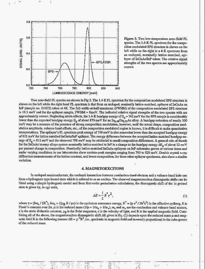
Figure 3. Two low-temperature zero-field PL spectra. The 1.4-K PL spectrum for the compo- sition modulated SPS structure is shown on the left while on the right is a 4-K spectrum from an undoped, nominally lattice matched, epi- layer of InGaAsDnP taken. The relative signal strengths of the two spectra are approximately correct.
Two zero-field PL spectra are shown in Fig 3. The 1.4-K PL spectrum for the composition modulated SPS structure is shown on the left while the right hand PL spectrum is that from an undoped, nominally lattice-matched, epilayer of InGaAs on InP (sample no. G1872) taken at 4K. The full-width-at-half-maximum 0 of the composition modulated SPS structure is 18.5 meV and for the epilayer sample, FWHM = 8meV. The indicated relative signal strengths of the two spectra with are approximately correct. Neglecting strain effects, the 1.4-K bandgap energy of Eg = 762 meV for the SPS sample is considerably lower than the expected bandgap energy Eg of about 870 meV for an h & 4 & ) 5 2 h alloy. A bandgap reduction of nearly 100 meV may be a measure of the presence of strong composition modulation, however, until the actual shape, composition mod- ulation amplitude, valenceband offsets, etc., of the composition modulated region is known, it is difficult to make quantitative interpretations. The epilayer's PL spectrum peak energy of 798 meV is also somewhat lower than the accepted bandgap energy of 812 meV for lattice matched InGaAsDnP epilayer. The energy difference between the accepted lattice matched bandgap en- ergy of Eg = 812 meV and the observed 798 meV may be attributih to small composition differences; A general rule of thumb for the InGaAs ternary alloys system nominally lattice matched to InP is a change to the bandgap energy AEg of about 12 meV per percent change in composition. Nominally latticematched InGaAs epilayers on InP substrates grown at various times and under varying conditions in our laboratories show exciton-peak energies ranging fiom 790 to 820 meV. Double crystal x-ray diffraction measurements of the lattice constant, and hence composition, for these other epilayer specimens, also show a similar variation.
4. MAGNETOEXCITONS In undoped semiconductors, the coulomb interaction between conduction-band electron and a valence-band hole can
form a hydrogenic type bound state which is referred to as an exciton. The observed magnetoexciton diamagnetic shifts can be fitted using a simple hydrogenic model and from first-order perturbation calculations, the diamagnetic shift of the 1s ground state is given by, in cgs units,
where y = (ha, / 2R*), hac = (2pp B / pc) is the cyclotron resonance energy, R* = (p e4 / 2fi2c2) is the effective rydberg, f i is Plank's constant over 27c, p is the reduced mass (Up = 11% + l/m,), m, and m, are the conduction and valence-band masses, E is the static dielectric constant, pp is the Bohr magneton, c is the velocity of light, and B is the applied magnetic field. Com- bining all of the above, the magnetoexciton diamagnetic shift AEi given in Eq. (1) depends upon the reduced mass p and mag- netic field B in the following manner AE = p-3B2, i.e., quadratic in magnetic field and inversely proportional to the cube-power of the reduced mass.
c
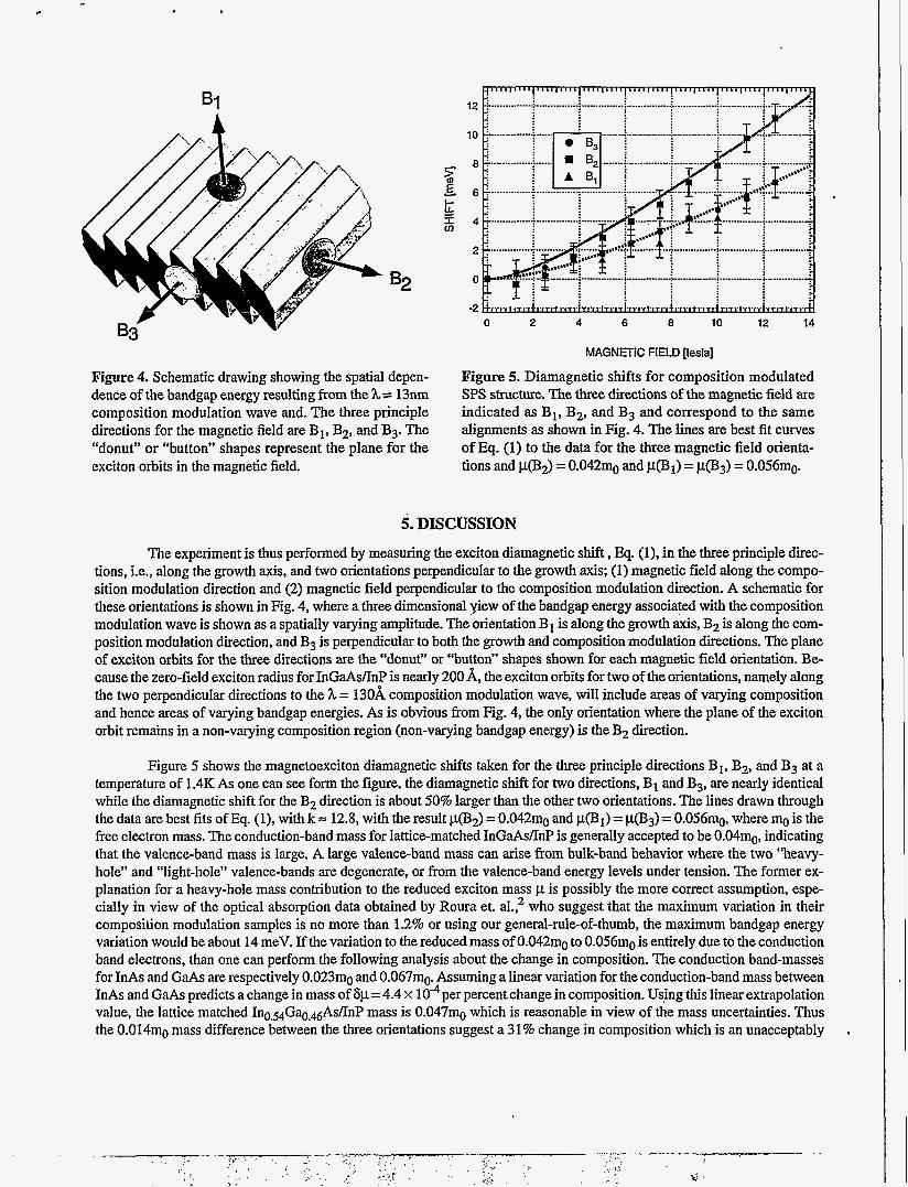
B1 A
Figure 4. Schematic drawing showing the spatial depen- dence of the bandgap energy resulting from the h= 13nm composition modulation wave and. The three principle directions for the magnetic field are B1, B2, and BJ. The “donut” or “button” shapes represent the plane for the exciton orbits in the magnetic field.
0 2 4 6 8 10 12 14
MAGNETIC FIELD [tesla]
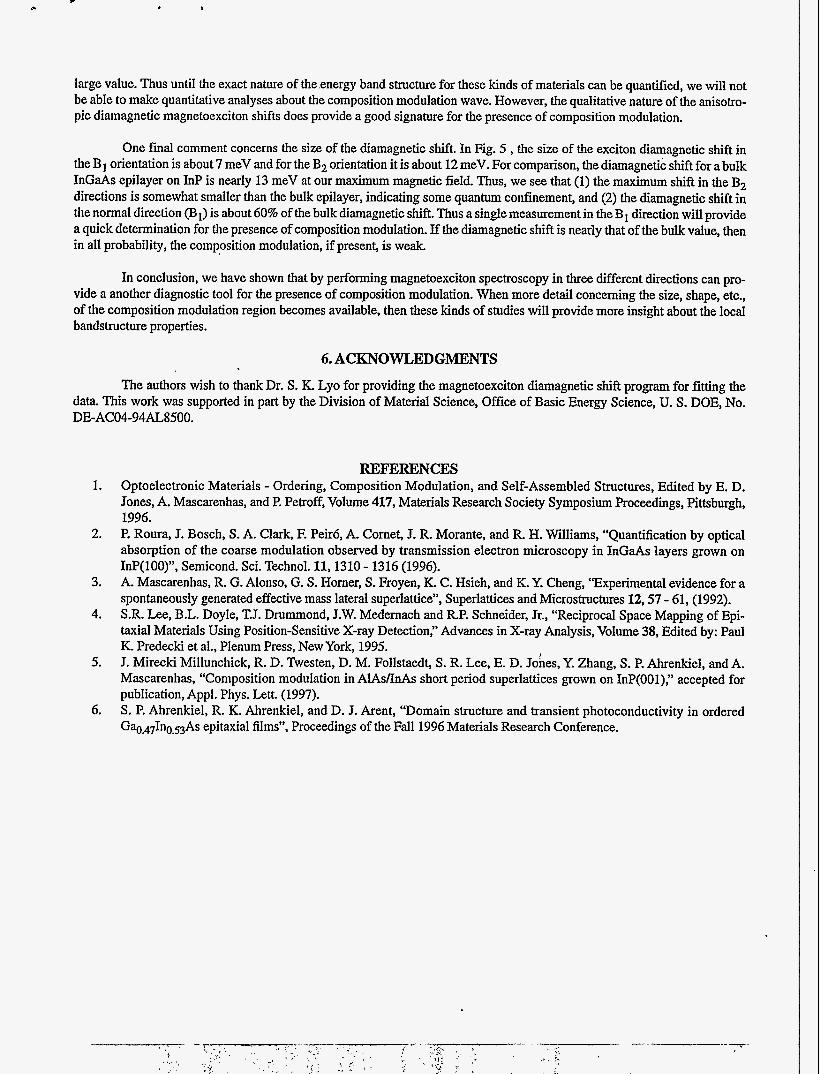
Figure 5. Diamagnetic shifts for composition modulated SPS structure. The three directions of the magnetic field are indicated as B1, B2, and B3 and correspond to the same alignments as shown in Fig. 4. The lines are best fit curves of Eq. (1) to the data for the three magnetic field orienta- tions and p(B2) = 0.042% and p(B,) = p(B3) = 0.056mo.
5. DISCUSSION The experiment is thus performed by measuring the exciton diamagnetic shift , Eq. (l), in the three principle direc-
tions, i.e., along the growth axis, and two orientations perpendicular to the growth axis; (1) magnetic field along the compo- sition modulation direction and (2) magnetic field perpendicular to the composition modulation direction. A schematic for these orientations is shown in Fig. 4, where a three dimensional yiew of the bandgap energy associated with the composition modulation wave is shown as a spatially varying amplitude. The orientation B1 is along the growth a&, B2 is along the com- position modulation direction, and B3 is perpendicular to both the growth and composition modulation directions. The plane of exciton orbits for the three directions are the “donut” or “button” shapes shown for each magnetic field orientation. Be- cause the zero-field exciton radius for InGaAsAd? is nearly 200 A, the exciton orbits for two of the orientations, namely along the two perpendicular directions to the h = 130A composition modulation wave, will include areas of varying composition and hence areas of varying bandgap energies. As is obvious from Fig. 4, the only orientation where the plane of the exciton orbit remains in a non-varying composition region (non-varying bandgap energy) is the B2 direction.
Figure 5 shows the magnetoexciton diamagnetic shifts taken for the three principle directions B1, B2, and B3 at a temperature of 1.4K As one can see form the figure, the diamagnetic shift for two directions, B1 and B3, are nearly identical while the diamagnetic shift for the B2 direction is about 50% larger than the other two orientations. The lines drawn through the data are best fits of Eq. (l), with k = 12.8, with the result p(B2) = 0.042% and p(B1) = p(B3) = 0.056%, where mo is the free electron mass. The conduction-band mass for lattice-matched InGaAsAnP is generally accepted to be 0.04m0, indicating that the valence-band mass is large. A large valence-band mass can arise from bulk-band behavior where the two “heavy- hole” and “light-hole,’ valence-bands are degenerate, or from the valence-band energy levels under tension. The former ex- planation for a heavy-hole mass contribution to the reduced exciton mass p is possibly the more correct assumption, espe- cially in view of the optical absorption data obtained by Roura et. al.? who suggest that the maximum variation in their composition modulation samples is no more than 1.2% or using our general-rule-of-thumb, the maximum bandgap energy variation would be about 14 meV. If the variation to the reduced mass of 0.042% to 0.056q is entirely due to the conduction band electrons, than one can perform the following analysis about the change in composition. The conduction band-masses for InAs and GaAs are respectively 0.023mo and 0.067m~ Assuming a linear variation for the conduction-band mass between InAs and GaAs predicts a change in mass of 6p= 4.4 X 10⁴per percent change in composition. Using this linear extrapolation value, the lattice matched In0.54G%.GAs/InP mass is 0.047mo which is reasonable in view of the mass uncertainties. Thus the 0.014mo mass difference between the three orientations suggest a 31% change in composition which is an unacceptably
large value. Thus until the exact nature of the.energy band structure for these kinds of materials can be quantified, we will not be able to make quantitative analyses about the composition modulation wave. However, the qualitative nature of the anisotro- pic diamagnetic magnetoexciton shifts does provide a good signature for the presence of composition modulation.
One final comment concerns the size of the diamagnetic shift. In Fig. 5 , the size of the exciton diamagnetic shift in the B1 orientation is about 7 meV and for the Bz orientation it is about 12 meV. For comparison, the diamagnetic shift for a bulk InGaAs epilayer on InP is nearly 13 meV at our maximum magnetic field. Thus, we see that (1) the maximum shift in the B2 directions is somewhat smaller than the bulk epilayer, indicating some quantum confinement, and (2) the diamagnetic shift in the normal direction (B is about 60% of the bulk diamagnetic shift. Thus a single measurement in the B, direction will provide a quick determination for the presence of composition modulation. If the diamagnetic shift is nearly that of the bulk value, then in all probability, the composition modulation, if present, is weak.
In conclusion, we have shown that by performing magnetoexciton spectroscopy in three different directions can pro- vide a another diagnostic tool for the presence of composition modulation. When more detail concerning the size, shape, etc., of the composition modulation region becomes available, then these kinds of studies will provide more insight about the local bandstructure properties.
6. ACKNOWLEDGMENTS The authors wish to thank Dr. S. K. Lyo for providing the magnetoexciton diamagnetic shift program for fitting the
data. This work was supported in part by the Division of Material Science, Office of Basic Energy Science, U. S. DOE, No. DE-AC04-94AL8500.
REFERENCES 1. Optoelectronic Materials - Ordering, Composition Modulation, and Self-Assembled Structures, Edited by E. D.
Jones, A. Mascarenhas, and P. Petroff, Volume 417, Materials Research Society Symposium Proceedings, Pittsburgh, 1996. P. Roura, J. Bosch, S. A. Clark, F. Peir6, A. Comet, J. R. Morante, and R H. Williams, “Quantification by optical absorption of the coarse modulation observed by transmission electron microscopy in InGaAs layers grown on InP(100)”, Semicond. Sci. Technol. 11,1310 - 1316 (1996). A. Mascarenhas, R. G. Alonso, G. S. Homer, S. Froyen, K. C. Hsieh, and K. Y. Cheng, “Experimental evidence for a spontaneously generated effective mass lateral superlattice”, Superlattices and Microstructures 12,57 - 61, (1992). S.R. Lee, B.L. Doyle, T.J. Drummond, J.W. Medemach and R.P. Schneider, Jr., “Reciprocal Space Mapping of Epi- taxial Materials Using Position-Sensitive X-ray Detection,” Advances in X-ray Analysis, Volume 38, Edited by: Paul K. Predecki et al., Plenum Press, New York, 1995. J. Mirecki Millunchick, R. D. Twesten, D. M. Follstaedt, S. R. Lee, E. D. Jones, Y. Zhang, S. P. Ahrenkiel, and A. Mascarenhas, “Composition modulation in AlAsAnAs short period superlattices grown on InP(001):’ accepted for publication, Appl. Phys. Lett. (1997). S. P. Ahrenkiel, R. K. Ahrenkiel, and D. J. Arent, “Domain structure and transient photoconductivity in ordered G%.@q,,,As epitaxial films”, Proceedings of the Fall 1996 Materials Research Conference.
2.
3.
4.
5.
6.


![Isotopic composition [ACE] Solar Modulation [PAMELA,ULYSSES]](https://static.fdocuments.net/doc/165x107/56814019550346895dab6670/isotopic-composition-ace-solar-modulation-pamelaulysses.jpg)
