Details of the First 3D-IC Multi-Project Wafer...
16
IEEE NSS-MIC, Knoxville, TN, USA, 30 Oct. - 6 Nov. 2010 1 email: [email protected] Details of the First 3D-IC Multi-Project Wafer Run OUTLINE: 1) involvement in 3D projects at Fermilab 2) 3D-IC consortium run 3) verification including 3D LVS 4) next steps 5) summary but no conclusions G. Deptuch, M.Demarteau, J.Hoff, R. Lipton, R. Patti 1 , A. Shenai, M. Trimpl, R.Yarema, T.Zimmerman 1 Tezzaron Semiconductor
Transcript of Details of the First 3D-IC Multi-Project Wafer...

IEEE NSS-MIC, Knoxville, TN, USA, 30 Oct. - 6 Nov. 2010
1email: [email protected]
Details of the First 3D-IC
Multi-Project Wafer Run
OUTLINE:
1) involvement in 3D projects at Fermilab
2) 3D-IC consortium run
3) verification including 3D LVS
4) next steps
5) summary but no conclusions
G. Deptuch, M.Demarteau, J.Hoff, R. Lipton, R. Patti1,
A. Shenai, M. Trimpl, R.Yarema, T.Zimmerman
1 Tezzaron Semiconductor

IEEE NSS-MIC, Knoxville, TN, USA, 30 Oct. - 6 Nov. 2010
2
Involvement in 3D projects at Fermilab
Two generations of Vertically Integrated Pixel (VIP1 & VIP2A) chips with
features for ILC detector vertex
1) run 3DM2;
to fab Oct. 2006 -> back Nov. 2007
2) and 3DM3;
to fab Oct. 2008 -> back Aug. 2010
VIA-LAST process (vias after bonding
and thinning) – excludes area for local
interconnect in TSV locations;
3 tiers (wafers) 180/150nm FDSOI
process with 3 regular metals and 2 tiers
with back-metal
SOI feature natural oxides = etch
stoppers and bonding surfaces
potential use of heteregenous wafers
Features:
Via Last

IEEE NSS-MIC, Knoxville, TN, USA, 30 Oct. - 6 Nov. 2010
3
Involvement in 3D projects at Fermilab
Sample
1
To analog output buses
VthDelay S. Trig
Sample 1
Sample
2
Pad to Sensor
Tier 3
Digital time stamp bus
Analog ramp bus
Write data
b0 Analog T.S.
Analog time stamp bus
Read data
In Out
Inject Pulse
Test input S. R.
Token in
X addesss
Y addressData
clock
Pixel
skip
logic
Token out
Read all
Read data
D FF
Q S
R
Tier 2
Tier 1
Thru
silicon
vias
b1 b2 b3 b4 b5 b6
D_Reset
Previous Hit AccumulationAccumulated Hit Signal
Tier C
“analog”
Tier B
“time stamp”
Tier A
“sparsify”
VIP = vertically integrated pixel – ILC type
Design from MIT-LL migrated to Tezz./Chartered
VIP2A
VIP1 found to be functional. Architecture proven but:VIP1 yield was low.VIP2A s submitted including adaptations
to analog design in FDSOI and played
safe face to laboratory scale processFocus has shifted from working in FD SOI to bulk CMOS processes
Decreasing threshold

IEEE NSS-MIC, Knoxville, TN, USA, 30 Oct. - 6 Nov. 2010
4
Involvement in 3D projects at Fermilab
VIP2A tests are showing
that 3D-IC technology works
Integrator response for 0fF and 20fF of input capacitance, Cin.
Noise as a function of sampling interval for Cin=20fF.
Pixel-pixel
discriminator
threshold
dispersions
300mVSingle pixel test structure
Full acquisition with
sparsified readout !!!

IEEE NSS-MIC, Knoxville, TN, USA, 30 Oct. - 6 Nov. 2010
5
3D-IC consortium run
Features:
0.13 mm bulk CMOS by Chartered with
Tezzaron 3D via-first technology
Via FirstMigrated VIP2A->VIP2B design
+ 2 other designs from Fermilab
and 9 other subreticules from
3D-IC consortium institutions
submitted on a Fermi MPW
1) to fab May/June 2009 -> back not yet
8” wafers, large ~26×31 mm2 reticule,
1P/6M (8M) + RDL, DNW, SM MIM Caps, LP
(chosen), standard VT + low VT, + Zero Vt +
IO MOSFETs, HR poly resistors,
embedded TSVs
Tungsten TSVs are part of the FEOL,
f=1.3 mm, 3.8 mm rec. spacing and 6 mm
depth,
6th metal used as a bond interface for
face-face Cu-Cu thermo-compression
bonding
After bonding, thinned to dashed line

IEEE NSS-MIC, Knoxville, TN, USA, 30 Oct. - 6 Nov. 2010
6
3D-IC consortium run
Alternative would be to fabricate two sets of wafers from two
sets of masks if there were enough customers
Economical solution employed on the 3D-IC run

IEEE NSS-MIC, Knoxville, TN, USA, 30 Oct. - 6 Nov. 2010
7
Full frame 0.13 mm
Chartered processVertical Symmetry
About Center
Test chips:
TX, TY
2.0 x 6.3 mm
Top tiers Bottom Tiers
Subreticules:
A, B, C, D, E,
F, G, H, I, J
5.5 x 6.3 mm
– Run organization:
• Consortium established by Fermilab in
late 2008, now 17 members; 6
countries (USA, Italy, France,
Germany, Poland, Canada)
• first designers’ meeting: Dec. 2008,
then Feb., Mar., and May 2009
• Initial designs for MPW run completed
in May 2009; 2 tier 3D chip, single
mask set face-to-face bonding;
Chartered 130 nm CMOS
• Numerous problems were
encountered with designs, software
tools at Tezzaron, shifting Chartered
requirements, etc.
• MPW frame accepted by Chartered in
March 2010, Waiting for chips –
Oct./Nov. 2010
• Delay appears related to
Global/Chartered decision to move
some equipment from prototype line,
where 3D wafers are done, to the
production line due to increase
production demands
3D-IC consortium run

IEEE NSS-MIC, Knoxville, TN, USA, 30 Oct. - 6 Nov. 2010
8
3D-IC consortium run – Depth of 3D-IC exploration:
• ideas for bonding fabricated chips to detectors were present from the beginning of chip design
• complexity of envisaged solutions was growing – from simple bonding apetite has grown to full double side connectivity
– Physical and functional verification
• continuous checking of designs by Fermilab and Tezzaron → identified numerous problems:+ layer map tables, bond interfaces,mirroring of designs in frame,+ different DRC violations found with Assura, Calibre, and Magma+ problems with CAD software MicroMagic, Calibre and Magma+ newer DRC versions uploaded
– Fabrication schedule
• order is for 31 wafers for all users
• 8 weeks for wafer fabrication.
• 4 weeks for 3D assembly
• 5 wafers for DBI try-out from Fermilab
Division of the frame into 12 subreticule pairs: left-right.
– Fermilab designs:
• H = VICTR; short pixel realizing pt cut for L1 trigger embedded in tracker for CMS @ SLHC
• I = VIP2b; time stamping pixel for vertex detector @ ILC
• J = VIPIC; very high frame rate with sparsification
pixel for Xray Photon Correlation Spectroscopy @ light source
• TX, TY test structures (single transistors and subcircuits)

IEEE NSS-MIC, Knoxville, TN, USA, 30 Oct. - 6 Nov. 2010
9
Verification including 3D LVS
NCSU merged global gds
Invoke Calibre /Assura
Run Calibre(NCSU)/Assura
LVS(FermiLab)
Schematic/Netlist
Are there
errors
reported?
Layout is
correct.
Highlight errors
Correct the errors
No
Yes
Fig. I: Basic LVS Flow Using Calibre or Assura
Open Layout
Invoke Calibre /Assura
Run Calibre/Assura LVS
Schematic/Netlist
Are there
errors
reported?
Layout is
correct.
Highlight errors
Correct the errors
No
Yes
Fig. 2: 3D LVS Flow Using Calibre or Assura
Run NCSU software to
create Tier0.gds &Tier1.gds
Open Layout
flow for 2D-IC
flow for 3D-IC
IEEE NSS-MIC, Knoxville, TN, USA, 30 Oct. - 6 Nov. 2010
10
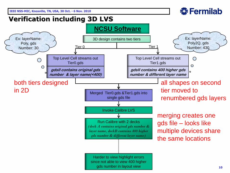
NCSU Software
Top Level Cell streams out
Tier0.gds
Top Level Cell streams out
Tier1.gds
3D design contains two tiers
gdsII contains original gds number & layer name(<400)
gdsII contains 400 higher gds number & different layer name
Merged Tier0.gds &Tier1.gds into
single gds file
Invoke Calibre LVS
Run Calibre with 2 decks(deck A contains original gds number &
layer name, deckB contains 400 higher
gds number & different layer name)
Tier 0 Tier 1
Harder to view highlight errors
since not able to view 400 higher
gds number in layout view
Ex: layerName:
Poly2Q, gds
Number: 430
Ex: layerName:
Poly, gds
Number: 30
Verification including 3D LVS
both tiers designed
in 2D
all shapes on second
tier moved to
renumbered gds layers
merging creates one
gds file – looks like
multiple devices share
the same locations

IEEE NSS-MIC, Knoxville, TN, USA, 30 Oct. - 6 Nov. 2010
11
Tier0: Fig. 3
Simple Inverter with 3 inter-tier connection (VDD, VSS, Tier0_out)
Tier1: Fig. 4
Inverter is flipped with 3 inter-tier connection (VDD, VSS, Tier1_in)
• Design contains two tiers(tier0 and tier1) & each tier design is top-level cell
• Don’t flip the design until after the LVS
• Connectivity are done between two tiers through Metal 6
• Sliding either direction tier0 or tier1 will connect both tiers VDD, VSS, and Tier0_out to Tier1_in
• Available pins after sliding: VDD, VSS, in, & out
No flipping, just
Slide to Tier1
No flipping, just
Slide to Tier0
VDD
VSS
Tier0_out
VDD
VSS
Tier1_in
Input pin: inOutput pin: out
See Fig. 3
Tier0: Inverter Layout
See Fig. 4
Tier1: Inverter Layout
Tier1_in
Tier0_out
Verification including 3D LVS

IEEE NSS-MIC, Knoxville, TN, USA, 30 Oct. - 6 Nov. 2010
12
Next steps•Preparation of sensors •Direct Bonding Interconnect (DBI®) by Ziptronix oxide-oxide W-to-W bonding
Detector wafer for 3D pixel chips from the MPW run
(Gabriela Carini, BNL )
Collaborative effort on the first 3D detector
for light source FNAL : BNL : AGH-UST
IEEE NSS-MIC, Knoxville, TN, USA, 30 Oct. - 6 Nov. 2010
13
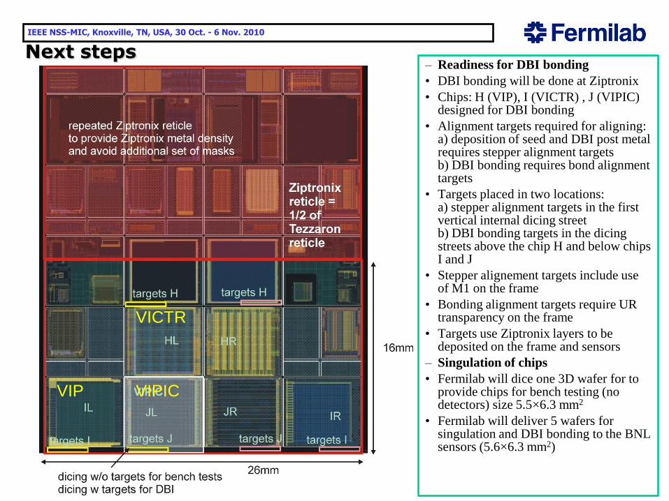
– Readiness for DBI bonding
• DBI bonding will be done at Ziptronix
• Chips: H (VIP), I (VICTR) , J (VIPIC) designed for DBI bonding
• Alignment targets required for aligning:a) deposition of seed and DBI post metal requires stepper alignment targets b) DBI bonding requires bond alignment targets
• Targets placed in two locations:a) stepper alignment targets in the first vertical internal dicing street b) DBI bonding targets in the dicing streets above the chip H and below chips I and J
• Stepper alignement targets include use of M1 on the frame
• Bonding alignment targets require UR transparency on the frame
• Targets use Ziptronix layers to be deposited on the frame and sensors
– Singulation of chips
• Fermilab will dice one 3D wafer for to provide chips for bench testing (no detectors) size 5.5×6.3 mm2
• Fermilab will deliver 5 wafers for singulation and DBI bonding to the BNL sensors (5.6×6.3 mm2)
Next steps
VICTR
VIP VIPIC

IEEE NSS-MIC, Knoxville, TN, USA, 30 Oct. - 6 Nov. 2010
14
Next steps
Fermilab, has worked closely with MOSIS/CMP and CMC to establish MPW runs for 3D circuits with commercial silicon brokers. Next submission of 3D chips planned for Spring 2011 via CMP/CMC/MOSIS partnership
• Developments for Future Runs– Chartered to stop TSVs on 8 inch
0.13 CMOS wafers for the foreseeable future
– Chartered agrees to process wafers from FEOL through M4
– Tezzaron will have SVTC add TSVs from M4 down into the substrate and complete the BEOL processing including the bond interface metalization
– Implication is that space will need to be left open on M1-M4 for the vias to pass through.
– Future potential benefit will be that wafers from other foundries can use the Tezzaron 3D process.
- 2 tier face to face bonded wafer
- 130 nm CMOS for both tiers
IEEE NSS-MIC, Knoxville, TN, USA, 30 Oct. - 6 Nov. 2010
15
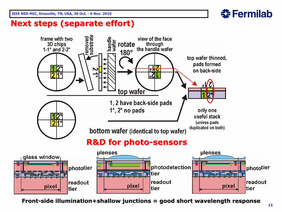
Next steps (separate effort)
R&D for photo-sensors
Front-side illumination+shallow junctions = good short wavelength response
photo photo

IEEE NSS-MIC, Knoxville, TN, USA, 30 Oct. - 6 Nov. 2010
16
Summary
.
Attempts made to explore the 3D technology has shown:
Successful Implementation of circuits
that go beyond the complexity of the test
structures and targeting real applications,
are achievable
The processing for 3D is new for the
industry (TSV cut, alignment, etc.); many
surprises are lurking on the users as the industry sticks to strict rules
and these rules are not yet settled for 3D techniques,
time needed for processing far exceeds initial estimations
There is no universal manufacturing
technology of integrated circuits 3D
– such a situation is expected
to maintain in the near future
It is not unreasonable to expect that with
the popularization of 3D techniques, which
undoubtedly will happen in the near future,
many of the problems find their solution
Commercial brokers MOSIS / CMP /
CMC have recognized opportunities
and decided to announce 3D MPW
service based on experience
Fermilab - the access to
the technology will be facilitatedThe first run has currently its wafers
being refabricated due to misalignment of reticles (targeting maximum # of
chips / wafer) preventing w-to-w bonding – priority at the fab;