Designing with the THS1206 High-Speed Data … 4 Designing With the THS1206 High-Speed Data...
29
Application Report SLAA094 - April 2000 1 Designing With the THS1206 High-Speed Data Converter Heinz-Peter Beckemeyer Advanced Analog Products ABSTRACT This application report is intended as a guide in the use of the digital and analog portions of the THS1206 A/D converter. On the digital portion, it discusses the main timing features to explain the requirements for initialization and operation. Two interface examples are presented where the THS1206 is connected to digital signal processors TMS320C54x and TMS320C6201. On the analog portion, it offers a discussion of the options to drive the THS1206 analog input. The system layout considerations presented will help achieve optimum system performance. Contents 1 Introduction 3 . . . . . . . . . . . . . . . . . . . . . . . . . . . . . . . . . . . . . . . . . . . . . . . . . . . . . . . . . . . . . . . . . . . . . . . . . 2 THS1206 Block Diagram 3 . . . . . . . . . . . . . . . . . . . . . . . . . . . . . . . . . . . . . . . . . . . . . . . . . . . . . . . . . . . . . . 3 Reset and Initialization 5 . . . . . . . . . . . . . . . . . . . . . . . . . . . . . . . . . . . . . . . . . . . . . . . . . . . . . . . . . . . . . . . 4 Integrated FIFO 6 . . . . . . . . . . . . . . . . . . . . . . . . . . . . . . . . . . . . . . . . . . . . . . . . . . . . . . . . . . . . . . . . . . . . . . 5 FIFO Reset 9 . . . . . . . . . . . . . . . . . . . . . . . . . . . . . . . . . . . . . . . . . . . . . . . . . . . . . . . . . . . . . . . . . . . . . . . . . . 6 Autoscan Mode 10 . . . . . . . . . . . . . . . . . . . . . . . . . . . . . . . . . . . . . . . . . . . . . . . . . . . . . . . . . . . . . . . . . . . . . 7 Control Signal DATA_AV 10 . . . . . . . . . . . . . . . . . . . . . . . . . . . . . . . . . . . . . . . . . . . . . . . . . . . . . . . . . . . . 8 Configuration of DATA_AV 11 . . . . . . . . . . . . . . . . . . . . . . . . . . . . . . . . . . . . . . . . . . . . . . . . . . . . . . . . . . 9 DATA_AV in Pulse Mode 12 . . . . . . . . . . . . . . . . . . . . . . . . . . . . . . . . . . . . . . . . . . . . . . . . . . . . . . . . . . . . . 10 DATA_AV in Static Mode 12 . . . . . . . . . . . . . . . . . . . . . . . . . . . . . . . . . . . . . . . . . . . . . . . . . . . . . . . . . . . . 11 Continuous-Conversion Mode 13 . . . . . . . . . . . . . . . . . . . . . . . . . . . . . . . . . . . . . . . . . . . . . . . . . . . . . . . 12 Single-Conversion Mode 14 . . . . . . . . . . . . . . . . . . . . . . . . . . . . . . . . . . . . . . . . . . . . . . . . . . . . . . . . . . . . 13 Reference Voltage 15 . . . . . . . . . . . . . . . . . . . . . . . . . . . . . . . . . . . . . . . . . . . . . . . . . . . . . . . . . . . . . . . . . . 14 Read-Back Mode 15 . . . . . . . . . . . . . . . . . . . . . . . . . . . . . . . . . . . . . . . . . . . . . . . . . . . . . . . . . . . . . . . . . . . 15 Test Mode 15 . . . . . . . . . . . . . . . . . . . . . . . . . . . . . . . . . . . . . . . . . . . . . . . . . . . . . . . . . . . . . . . . . . . . . . . . . . 16 Overflow Flag 16 . . . . . . . . . . . . . . . . . . . . . . . . . . . . . . . . . . . . . . . . . . . . . . . . . . . . . . . . . . . . . . . . . . . . . . 17 Equivalent Analog Input Schematic 16 . . . . . . . . . . . . . . . . . . . . . . . . . . . . . . . . . . . . . . . . . . . . . . . . . . 18 Analog Input Configuration 17 . . . . . . . . . . . . . . . . . . . . . . . . . . . . . . . . . . . . . . . . . . . . . . . . . . . . . . . . . . 18.1 Single-Ended Mode 18 . . . . . . . . . . . . . . . . . . . . . . . . . . . . . . . . . . . . . . . . . . . . . . . . . . . . . . . . . . . . . 18.2 DC Coupling 18 . . . . . . . . . . . . . . . . . . . . . . . . . . . . . . . . . . . . . . . . . . . . . . . . . . . . . . . . . . . . . . . . . . . 18.3 AC-Coupled Input 19 . . . . . . . . . . . . . . . . . . . . . . . . . . . . . . . . . . . . . . . . . . . . . . . . . . . . . . . . . . . . . . . 18.4 Differential Mode 19 . . . . . . . . . . . . . . . . . . . . . . . . . . . . . . . . . . . . . . . . . . . . . . . . . . . . . . . . . . . . . . . . 19 Layout Considerations 20 . . . . . . . . . . . . . . . . . . . . . . . . . . . . . . . . . . . . . . . . . . . . . . . . . . . . . . . . . . . . . .
Transcript of Designing with the THS1206 High-Speed Data … 4 Designing With the THS1206 High-Speed Data...
Application ReportSLAA094 - April 2000
1
Designing With the THS1206 High-Speed Data ConverterHeinz-Peter Beckemeyer Advanced Analog Products
ABSTRACT
This application report is intended as a guide in the use of the digital and analog portions ofthe THS1206 A/D converter. On the digital portion, it discusses the main timing features toexplain the requirements for initialization and operation. Two interface examples arepresented where the THS1206 is connected to digital signal processors TMS320C54x andTMS320C6201. On the analog portion, it offers a discussion of the options to drive theTHS1206 analog input. The system layout considerations presented will help achieveoptimum system performance.
Contents
1 Introduction 3. . . . . . . . . . . . . . . . . . . . . . . . . . . . . . . . . . . . . . . . . . . . . . . . . . . . . . . . . . . . . . . . . . . . . . . . .
2 THS1206 Block Diagram 3. . . . . . . . . . . . . . . . . . . . . . . . . . . . . . . . . . . . . . . . . . . . . . . . . . . . . . . . . . . . . .
3 Reset and Initialization 5. . . . . . . . . . . . . . . . . . . . . . . . . . . . . . . . . . . . . . . . . . . . . . . . . . . . . . . . . . . . . . .
4 Integrated FIFO 6. . . . . . . . . . . . . . . . . . . . . . . . . . . . . . . . . . . . . . . . . . . . . . . . . . . . . . . . . . . . . . . . . . . . . .
5 FIFO Reset 9. . . . . . . . . . . . . . . . . . . . . . . . . . . . . . . . . . . . . . . . . . . . . . . . . . . . . . . . . . . . . . . . . . . . . . . . . .
6 Autoscan Mode 10. . . . . . . . . . . . . . . . . . . . . . . . . . . . . . . . . . . . . . . . . . . . . . . . . . . . . . . . . . . . . . . . . . . . .
7 Control Signal DATA_AV 10. . . . . . . . . . . . . . . . . . . . . . . . . . . . . . . . . . . . . . . . . . . . . . . . . . . . . . . . . . . .
8 Configuration of DATA_AV 11. . . . . . . . . . . . . . . . . . . . . . . . . . . . . . . . . . . . . . . . . . . . . . . . . . . . . . . . . .
9 DATA_AV in Pulse Mode 12. . . . . . . . . . . . . . . . . . . . . . . . . . . . . . . . . . . . . . . . . . . . . . . . . . . . . . . . . . . . .
10 DATA_AV in Static Mode 12. . . . . . . . . . . . . . . . . . . . . . . . . . . . . . . . . . . . . . . . . . . . . . . . . . . . . . . . . . . .
11 Continuous-Conversion Mode 13. . . . . . . . . . . . . . . . . . . . . . . . . . . . . . . . . . . . . . . . . . . . . . . . . . . . . . .
12 Single-Conversion Mode 14. . . . . . . . . . . . . . . . . . . . . . . . . . . . . . . . . . . . . . . . . . . . . . . . . . . . . . . . . . . .
13 Reference Voltage 15. . . . . . . . . . . . . . . . . . . . . . . . . . . . . . . . . . . . . . . . . . . . . . . . . . . . . . . . . . . . . . . . . .
14 Read-Back Mode 15. . . . . . . . . . . . . . . . . . . . . . . . . . . . . . . . . . . . . . . . . . . . . . . . . . . . . . . . . . . . . . . . . . .
15 Test Mode 15. . . . . . . . . . . . . . . . . . . . . . . . . . . . . . . . . . . . . . . . . . . . . . . . . . . . . . . . . . . . . . . . . . . . . . . . . .
16 Overflow Flag 16. . . . . . . . . . . . . . . . . . . . . . . . . . . . . . . . . . . . . . . . . . . . . . . . . . . . . . . . . . . . . . . . . . . . . .
17 Equivalent Analog Input Schematic 16. . . . . . . . . . . . . . . . . . . . . . . . . . . . . . . . . . . . . . . . . . . . . . . . . .
18 Analog Input Configuration 17. . . . . . . . . . . . . . . . . . . . . . . . . . . . . . . . . . . . . . . . . . . . . . . . . . . . . . . . . . 18.1 Single-Ended Mode 18. . . . . . . . . . . . . . . . . . . . . . . . . . . . . . . . . . . . . . . . . . . . . . . . . . . . . . . . . . . . . 18.2 DC Coupling 18. . . . . . . . . . . . . . . . . . . . . . . . . . . . . . . . . . . . . . . . . . . . . . . . . . . . . . . . . . . . . . . . . . . 18.3 AC-Coupled Input 19. . . . . . . . . . . . . . . . . . . . . . . . . . . . . . . . . . . . . . . . . . . . . . . . . . . . . . . . . . . . . . . 18.4 Differential Mode 19. . . . . . . . . . . . . . . . . . . . . . . . . . . . . . . . . . . . . . . . . . . . . . . . . . . . . . . . . . . . . . . .
19 Layout Considerations 20. . . . . . . . . . . . . . . . . . . . . . . . . . . . . . . . . . . . . . . . . . . . . . . . . . . . . . . . . . . . . .

SLAA094
2 Designing With the THS1206 High-Speed Data Converter
20 Parallel Interface 23. . . . . . . . . . . . . . . . . . . . . . . . . . . . . . . . . . . . . . . . . . . . . . . . . . . . . . . . . . . . . . . . . . . .
21 Interfacing the THS1206 to the TMS320VC5402 23. . . . . . . . . . . . . . . . . . . . . . . . . . . . . . . . . . . . . . .
22 Interfacing the THS1206 to the TMS320C6211 25. . . . . . . . . . . . . . . . . . . . . . . . . . . . . . . . . . . . . . . . .
23 Summary 27. . . . . . . . . . . . . . . . . . . . . . . . . . . . . . . . . . . . . . . . . . . . . . . . . . . . . . . . . . . . . . . . . . . . . . . . . . .
24 References 28. . . . . . . . . . . . . . . . . . . . . . . . . . . . . . . . . . . . . . . . . . . . . . . . . . . . . . . . . . . . . . . . . . . . . . . . .
25 Glossary 28. . . . . . . . . . . . . . . . . . . . . . . . . . . . . . . . . . . . . . . . . . . . . . . . . . . . . . . . . . . . . . . . . . . . . . . . . . .
List of Figures
1 THS1206 Block Diagram 4. . . . . . . . . . . . . . . . . . . . . . . . . . . . . . . . . . . . . . . . . . . . . . . . . . . . . . . . . . . . . . . . . 2 THS1206 Initialization 6. . . . . . . . . . . . . . . . . . . . . . . . . . . . . . . . . . . . . . . . . . . . . . . . . . . . . . . . . . . . . . . . . . . 3 The FIFO as a Circular Buffer 7. . . . . . . . . . . . . . . . . . . . . . . . . . . . . . . . . . . . . . . . . . . . . . . . . . . . . . . . . . . . . 4 Example With Four Analog Inputs and a Trigger Level of 8 8. . . . . . . . . . . . . . . . . . . . . . . . . . . . . . . . . . . 5 Reading the FIFO Data in a Burst at 2 MSPS 9. . . . . . . . . . . . . . . . . . . . . . . . . . . . . . . . . . . . . . . . . . . . . . . 6 Reading the FIFO Data in a Burst at 6 MSPS 9. . . . . . . . . . . . . . . . . . . . . . . . . . . . . . . . . . . . . . . . . . . . . . . 7 Autoscan Mode for TL = 8 and Four Analog Inputs 10. . . . . . . . . . . . . . . . . . . . . . . . . . . . . . . . . . . . . . . . . 8 DATA_AV (In Active-Low, Pulse Configuration) After Reset 11. . . . . . . . . . . . . . . . . . . . . . . . . . . . . . . . . . 9 Timing of DATA_AV in Pulse Mode 12. . . . . . . . . . . . . . . . . . . . . . . . . . . . . . . . . . . . . . . . . . . . . . . . . . . . . . . 10 Timing of DATA_AV in Pulse Mode With Early Read 12. . . . . . . . . . . . . . . . . . . . . . . . . . . . . . . . . . . . . . . 11 Timing of DATA_AV in Static Mode 12. . . . . . . . . . . . . . . . . . . . . . . . . . . . . . . . . . . . . . . . . . . . . . . . . . . . . . 12 Timing of Continuous-Conversion Mode (One-Channel Operation) 13. . . . . . . . . . . . . . . . . . . . . . . . . . 13 Timing of Continuous-Conversion Mode (Four-Channel Operation) 14. . . . . . . . . . . . . . . . . . . . . . . . . . 14 Timing of Single-Conversion Mode 14. . . . . . . . . . . . . . . . . . . . . . . . . . . . . . . . . . . . . . . . . . . . . . . . . . . . . . 15 Equivalent Analog Schematic 16. . . . . . . . . . . . . . . . . . . . . . . . . . . . . . . . . . . . . . . . . . . . . . . . . . . . . . . . . . . 16 Single-Ended Input Stage 17. . . . . . . . . . . . . . . . . . . . . . . . . . . . . . . . . . . . . . . . . . . . . . . . . . . . . . . . . . . . . . 17 Differential Input Stage 17. . . . . . . . . . . . . . . . . . . . . . . . . . . . . . . . . . . . . . . . . . . . . . . . . . . . . . . . . . . . . . . . 18 Level Shift for DC-Coupled Input 18. . . . . . . . . . . . . . . . . . . . . . . . . . . . . . . . . . . . . . . . . . . . . . . . . . . . . . . . 19 AC-Coupled Input 19. . . . . . . . . . . . . . . . . . . . . . . . . . . . . . . . . . . . . . . . . . . . . . . . . . . . . . . . . . . . . . . . . . . . . 20 Single-Ended to Differential Conversion by Transformer 19. . . . . . . . . . . . . . . . . . . . . . . . . . . . . . . . . . . . 21 Mixed-Signal Four-Layer Board 20. . . . . . . . . . . . . . . . . . . . . . . . . . . . . . . . . . . . . . . . . . . . . . . . . . . . . . . . . 22 Recommendation for Ground Planes 21. . . . . . . . . . . . . . . . . . . . . . . . . . . . . . . . . . . . . . . . . . . . . . . . . . . . 23 Common Supply for a Mixed Signal Design 22. . . . . . . . . . . . . . . . . . . . . . . . . . . . . . . . . . . . . . . . . . . . . . 24 Use of Bypassing With The THS1206 22. . . . . . . . . . . . . . . . . . . . . . . . . . . . . . . . . . . . . . . . . . . . . . . . . . . 25 Logical Combination of CS0, CS1, RD, and WR 23. . . . . . . . . . . . . . . . . . . . . . . . . . . . . . . . . . . . . . . . . . 26 Interfacing the THS2106 to the TMS320VC5402 24. . . . . . . . . . . . . . . . . . . . . . . . . . . . . . . . . . . . . . . . . . 27 Write Access to the THS1206 (CS0-IOSTRB-Controlled) 24. . . . . . . . . . . . . . . . . . . . . . . . . . . . . . . . . . . 28 Read Access to the THS1206 (CS0-IOSTRB-Controlled) 25. . . . . . . . . . . . . . . . . . . . . . . . . . . . . . . . . . . 29 Interfacing the THS1206 to the TMS320C6211 25. . . . . . . . . . . . . . . . . . . . . . . . . . . . . . . . . . . . . . . . . . . 30 Write Access to the THS1206 (WR-AWE-Controlled) 26. . . . . . . . . . . . . . . . . . . . . . . . . . . . . . . . . . . . . . 31 Read Access to the THS1206 (RD-ARE-Controlled) 27. . . . . . . . . . . . . . . . . . . . . . . . . . . . . . . . . . . . . . .
List of Tables
1 Control Register 0 (CR0) 5. . . . . . . . . . . . . . . . . . . . . . . . . . . . . . . . . . . . . . . . . . . . . . . . . . . . . . . . . . . . . . . . . 2 Control Register 1 (CR1) 5. . . . . . . . . . . . . . . . . . . . . . . . . . . . . . . . . . . . . . . . . . . . . . . . . . . . . . . . . . . . . . . . . 3 Control Register Addressing 5. . . . . . . . . . . . . . . . . . . . . . . . . . . . . . . . . . . . . . . . . . . . . . . . . . . . . . . . . . . . . .
SLAA094
3 Designing With the THS1206 High-Speed Data Converter
4 FIFO Trigger Level 7. . . . . . . . . . . . . . . . . . . . . . . . . . . . . . . . . . . . . . . . . . . . . . . . . . . . . . . . . . . . . . . . . . . . . 5 Configuration of DATA_AV 11. . . . . . . . . . . . . . . . . . . . . . . . . . . . . . . . . . . . . . . . . . . . . . . . . . . . . . . . . . . . . . 6 Test Modes of the THS1206 15. . . . . . . . . . . . . . . . . . . . . . . . . . . . . . . . . . . . . . . . . . . . . . . . . . . . . . . . . . . . .
1 Introduction
The THS1206 is a low-power, 12-bit, 6-MSPS analog-to-digital converter (ADC). Its mainfeatures include four analog inputs, which are switched from sampling to hold modesimultaneously, fast speed, high resolution, and high data throughput. These features make theTHS1206 very attractive in radar, imaging, high-speed acquisition, communications, and controlapplications. The THS1206, with its programmable interface, is designed to be compatible withmultiple processors on the market. A fast data throughput to the connected processor isachieved with an integrated FIFO.
2 THS1206 Block Diagram
Figure 1 shows the THS1206 block diagram. The analog-to-digital converter (ADC) is built as amultistage pipelined architecture using output error correction logic to assure code integrity overthe full operating temperature range. The ADC has 12 bits of resolution and a maximumconversion rate up to 6 MSPS (megasamples per second). The main feature of the analogportion of the THS1206 is its four analog input stages, which are simultaneously switched fromsampling to hold mode. These stages can be selected individually and configured assingle-ended, as differential inputs, or as a combination of both. This feature makes the deviceattractive for use in control applications as well as in conversion of I/Q-modulated signals. Thephase relation between the analog inputs is important in these applications. An internalreference voltage (1.5 V or 3.5 V) is provided to reduce the amount of external components.However, an external-reference voltage can also be chosen to match the dc-accuracy of theapplication. The common-mode voltage of the internal reference is available at REFOUT. If thisoutput is used as a system reference signal, it can be utilized to bias single-supply operationalamplifiers, or to set the common-mode voltage at the output of a transformer for use in theanalog input path.
SLAA094
4 Designing With the THS1206 High-Speed Data Converter
1.225 VReference
S/H
12 BitPipeline
ADC
+
–
SingleEndedand/or
DiffMUX
S/H
S/H
S/H
FIFO16 × 12
12
Buffers
Logicand
Control
ControlRegister
AVDD DVDD
REFP
REFM
REFINAINP
AINM
BINP
BINM
CONV_CLK (CONVST)
CS0
CS1
RD
WR (R/W)
AGND DGND
REFOUT
DATA_AV
BVDDD0D1D2D3D4D5D6D7D8D9D10/RA0D11/RA1
BGND
3.5 V
1.5 VVREFP
2.5 V
VREFM
Figure 1. THS1206 Block Diagram
Another important feature of the THS1206 is its 16-word 12-bit FIFO. The FIFO takes the loadoff the processor connected to the ADC. Data can be transferred in bust mode, greatlyimproving the data throughput to the processor. The THS1206 interface to the processor is veryflexible and can be configured, offering the possibility of glueless interface to modernprocessors. The digital conversion result is provided in parallel data format via data bus pinsD0 – D11.
Two different conversion modes can be selected: single and continuous. In the single-conversion mode, a single simultaneous conversion of up to four analog input channels can beinitiated by the single-conversion start signal (CONVST). The conversion clock in thesingle-conversion mode is generated internally using a clock oscillator circuit. Thesingle-conversion mode is specifically used in control applications. In the continuous-conversionmode, an external clock signal is applied to the CONV_CLK input of the THS1206. The internalclock oscillator is switched off in this mode. The continuous-conversion mode is specifically usedin applications where a block of data must be converted from analog to digital format, forexample when a window of 2048 words is used in a fast fourier transformation (FFT). Twointernal control registers are used to configure the conversion modes of the THS1206.
SLAA094
5 Designing With the THS1206 High-Speed Data Converter
3 Reset and Initialization
The THS1206 contains two internal control registers (control register 0 and 1). These registersare required to configure the THS1206 to the desired mode and to reset the device. TheTHS1206 should be reset at the beginning of initialization. Reset is performed by writing 0x401hto control register 1. Control registers 0 and 1 are 10-bits wide and can be accessed via theTHS1206 parallel data bus D0 to D11. Tables 1 and 2 show the individual bits of controlregisters 0 and 1. The THS1206 data sheet presents a description of each bit.
Table 1. Control Register 0 (CR0)
Bit 9 Bit 8 Bit 7 Bit 6 Bit 5 Bit 4 Bit 3 Bit 2 Bit 1 Bit 0
TEST1 TEST0 SCAN DIFF1 DIFF0 CHSEL1 CHSEL0 PD MODE VREF
Table 2. Control Register 1 (CR1)
Bit 9 Bit 8 Bit 7 Bit 6 Bit 5 Bit 4 Bit 3 Bit 2 Bit 1 Bit 0
RBACK OFFSET BIN/2s R/W DATA_P DATA_T TRIG1 TRIG0 OVFL/FRST RESET
Upper bits D10 and D11 are used for the control register address, whereas the control registervalue is contained in data bits D0 to D9 during the write process. Table 3 shows the controlregister addressing.
Table 3. Control Register Addressing
D0 – D9 D10/RA0 D11/RA1 ADDRESSED CONTROL REGISTER
Desired register value 0 0 Control Register 0 (CR0)
Desired register value 1 0 Control Register 1 (CR1)
Data bit D11/RA1 is reserved and should always be zero.

SLAA094
6 Designing With the THS1206 High-Speed Data Converter
The THS1206 should be initialized in the following sequence:
Start
Use DefaultValues?
Yes
Write 0x401 toTHS1206
(Set Reset Bit in CR1)
No
Write 0x401 toTHS1206
(Set Reset Bit inCR1)
Clear RESET byWriting 0x400 to
CR1
Write the UserConfiguration to
CR0
Write the UserConfiguration toCR1 (Can IncludeFIFO Reset, MustExclude Reset)
Continue
Clear RESET byWriting 0x400 to
CR1
Figure 2. THS1206 Initialization
The default values are defined in the data sheet.
4 Integrated FIFO
The THS1206 has an integrated FIFO which is organized as a circular buffer in order to achievethe higher data throughputs required by today’s processors. This circular buffer can store up to16 samples. A new sample is written to the FIFO with every falling edge of the conversion clock(CONV_CLK). The FIFO has a flexible and configurable design, and it allows overwriting. Thislast feature can be particularly interesting in applications where data must be collected at certainintervals. The data read by the processor should always be the latest data, which is assured bythe special circular buffer structure. Overwriting during the relevant intervals is prevented by fastreading the stored data.
Figure 3 shows the structure of the THS1206 FIFO. It is arranged so that sample reading takesplace asynchronously to the sampling clock CONV_CLK.

SLAA094
7 Designing With the THS1206 High-Speed Data Converter
8910
11
12
13
14
1516 1
2
3
4
5
6
7
Read Pointer
Trigger Pointer
Write Pointer
Data in FIFO
Free
Figure 3. The FIFO as a Circular Buffer
Samples are automatically written to the FIFO. Write, read, and trigger pointers are used tocontrol the writing and reading processes. The read pointer always points to the next location tobe read. The write pointer always points to the location which contains the last written sample.With a selection of multiple analog input channels, the converted values are written to thecircular buffer in a predefined sequence (autoscan mode). In this way, the channel informationfor the reading processor is continuously maintained.
A specific storage depth (trigger level) must be selected for the circular buffer. When this level isreached, the THS1206 signals the connected processor via the digital output DATA_AV (dataavailable) that a block of conversion values is ready to be transferred. The block size to be readis always equal to the setting of the trigger level; this is important in order to maintain thechannel information when multiple channels are selected. Table 4 shows the trigger levelsavailable with each particular number of analog inputs selected.
Table 4. FIFO Trigger Level
BIT 3TRIG1
BIT 2TRIG0
TRIGGER LEVELFOR 1 CHANNEL
TRIGGER LEVELFOR 2 CHANNELS
TRIGGER LEVELFOR 3 CHANNELS
TRIGGER LEVELFOR 4 CHANNELS
0 0 01 02 03 04
0 1 04 04 06 08
1 0 08 08 09 12
1 1 14 12 12 Reserved
Let’s consider a specific example where all four analog input channels (AINP, AINM, BINP andBINM) are selected and the trigger level is set to 8. The samples are written to the FIFOaccording to the autoscan mode. The signal DATA_AV becomes active when the write pointerreaches the trigger pointer. Using DATA_AV as an interrupt, the processor is immediately able toread the eight-word block and the trigger pointer will be incremented by 8 (see Figure 4). If theprocessor can not read the data immediately, new samples are written to the FIFO and thetrigger and read pointers stay at the same location. Thus, when the write pointer returns tolocation 1, the four oldest data samples in the FIFO are overwritten. At this time, the read pointerand the trigger pointer are incremented by the number of selected channels (four in thisexample) in order to maintain the channel information.

SLAA094
8 Designing With the THS1206 High-Speed Data Converter
910
11
12
13
14
1516 AINP
AINM
BINP
BINM
AINP
AINM
BINPBINM
ReadPointer
Trigger Pointer
PointerMoves WithFirst Read
Write Pointer
Figure 4. Example With Four Analog Inputs and a Trigger Level of 8
The programmable storage depth allows for adjustment to different processors. This techniquestrongly reduces the burden on the processor. The THS1206 data is transferred in batches bymeans of the integrated FIFO and its control logic. This represents the optimum use of theinterface between the THS1206 and the processor.
A problem may be found with timely transfer of samples from the A/D processor when theconversion rate is above 1 MSPS. The data is normally transferred from the A/D converter to theprocessor during an interrupt-service routine (ISR). However, the maximum speed is somehowlimited, as every processor exhibits a latency time (the time required for first possible accessduring the ISR). The latency time can amount to as much as a hundred nanoseconds,depending on the particular processor and on its frequency. The resulting speed is therebylimited to 1 MHz to 2 MHz. This creates the problems of selecting data, which is controlled viaan interrupt from a fast A/D converter, and of further processing this data afterwards. Figures 5and 6 give a more detailed explanation of this issue.
Figure 5 shows a measurement taken with the THS1206 connected to the TMS320C542 DSP,which has a cycle time of 25 ns. The clock signal CONV_CLK is set to 2 MHz in this example.The resultant DSP latency time due to the interrupt service routine within the DSP (time fromDATA_AV falling edge to RD falling edge) is approximately 400 ns. This means that the DSP willnot be able to read the data from the THS1206 within one CONV_CLK cycle if the processor hasto jump into an interrupt service routine for every conversion value.
The FIFO incorporated in the THS1206 allows the processor to read the conversion values in aburst. Data reading in burst mode increases the data throughput, because the latency time ofthe processor is seen only once per burst.

SLAA094
9 Designing With the THS1206 High-Speed Data Converter
tLAT
CONV_CLK
DATA_AV
RD
WR
CONV_CLK = 2 MHz
Figure 5. Reading the FIFO Data in a Burst at 2 MSPS
Figures 5 illustrates an example of burst reading of the THS1206 FIFO data. The FIFO triggerlevel is set to 8 in this example. This means that signal DATA_AV becomes active after writingeight values to the FIFO. Therefore, the processor must read eight values from the THS1206within one ISR. In order to achieve the required data throughput from the THS1206 to the DSP,the DSP must be able to read all the samples before the next DATA_AV becomes active. This2-MHz sampling frequency is only possible if reading occurs in a burst. Therefore, this approachincreases the maximum data throughput.
tLAT
CONV_CLK
DATA_AV
RD
WR
CONV_CLK = 6 MHz
Figure 6. Reading the FIFO Data in a Burst at 6 MSPS
Figure 6 shows a measurement taken with the same THS1206 to TMS320C542 DSP interface,but using a sampling frequency of 6 MSPS. It can be observed that the processor is just able tocatch the block of data between of two DATA_AV signals, which is a requirement in order to readthe data from the ADC. This roughly determines the maximum data throughput between theTHS1206 and the TMS320C542, with 25 ns cycle time for this mode of operation. Typically, atrigger level of 8 (9 for three analog input channels) is the best choice for an optimized datatransfer rate.
5 FIFO Reset
A reset of the FIFO is typically performed when configuring the THS1206 during the last step ofthe initialization routine. A reset can also be performed at any other time, and it is particularlyrecommended when the ADC is only active during a specific time frame so that an overflowwithin the FIFO occurs. An example of this is the continuous reading of a block of data (such as4K of data for a FFT) over a given period of time. Before the THS1206 starts on a new block ofdata, a reset should be initiated in order to reset the internal FIFO pointer and the DATA_AVsignal.

SLAA094
10 Designing With the THS1206 High-Speed Data Converter
6 Autoscan Mode
The autoscan mode is required in order to achieve channel integrity. In a multichannel operation,data is always written to the FIFO in a predefined sequence. Therefore, the processor alwayshas to read a specific number of samples equal to the trigger level (TL) selected in order to havethe channel information.
859 1C1 F31 3C4 859 1C1 F31 3C4 859 1C1 F31 3C4 859 1C1 F31
DataAINM
DataBINM
DataAINM
DataBINM
DataAINP
DataBINP
DataAINP
DataBINP
CONV_CLK
DATA_AV
RD
WR
DATA
Figure 7. Autoscan Mode for TL = 8 and Four Analog Inputs
Using four analog input channels and a trigger level of eight as an example, the processor hasto read within each interrupt service routine, as illustrated in Figure 7. The first data read afterDATA_AV becomes active belongs to channel AINP. This remains valid as long as the processorreads a number of times equal to the trigger level (TL) for every activation of DATA_AV.
7 Control Signal DATA_AV
DATA_AV (data available) can be used as a control signal to indicate the processor that data isready to be read from the FIFO. DATA_AV can be programmed in a flexible way. This sectiongives detailed information on the possible configurations and on the behavior of DATA_AV afterreset and during operation.
DATA_AV becomes active when the write pointer associated with the FIFO reaches the triggerpointer. Since the write pointer is incremented with every clock cycle, there is a relation betweenthe conversion clock CONV_CLK and signal DATA_AV. The number of clock cycles until thesignal DATA_AV becomes active is equal to the selected trigger level (TL). This relationshipremains true as long as the processor can read the data from the THS1206 on time.
However, the behavior is different after reset of the THS1206. The first conversion value iswritten to the FIFO with a delay (latency) caused by the pipeline architecture and the resetarchitecture of the THS1206. DATA_AV becomes active 7 + TL conversion clock cycles afterreset.
SLAA094
11 Designing With the THS1206 High-Speed Data Converter
1 2 3 4 5 6 7 8 9 10 11
RESET
ClearRESET
CR0
CR1
CONV_CLK
DATA_AV
RD
WR
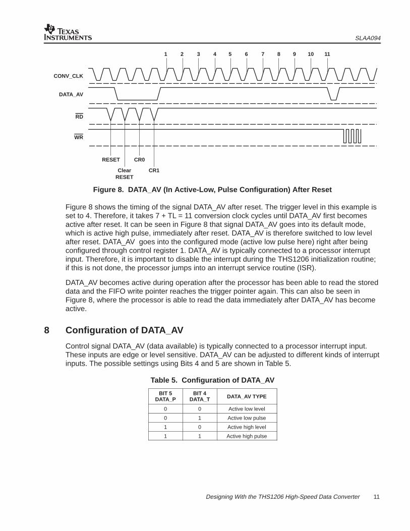
Figure 8. DATA_AV (In Active-Low, Pulse Configuration) After Reset
Figure 8 shows the timing of the signal DATA_AV after reset. The trigger level in this example isset to 4. Therefore, it takes 7 + TL = 11 conversion clock cycles until DATA_AV first becomesactive after reset. It can be seen in Figure 8 that signal DATA_AV goes into its default mode,which is active high pulse, immediately after reset. DATA_AV is therefore switched to low levelafter reset. DATA_AV goes into the configured mode (active low pulse here) right after beingconfigured through control register 1. DATA_AV is typically connected to a processor interruptinput. Therefore, it is important to disable the interrupt during the THS1206 initialization routine;if this is not done, the processor jumps into an interrupt service routine (ISR).
DATA_AV becomes active during operation after the processor has been able to read the storeddata and the FIFO write pointer reaches the trigger pointer again. This can also be seen inFigure 8, where the processor is able to read the data immediately after DATA_AV has becomeactive.
8 Configuration of DATA_AV
Control signal DATA_AV (data available) is typically connected to a processor interrupt input.These inputs are edge or level sensitive. DATA_AV can be adjusted to different kinds of interruptinputs. The possible settings using Bits 4 and 5 are shown in Table 5.
Table 5. Configuration of DATA_AV
BIT 5DATA_P
BIT 4DATA_T DATA_AV TYPE
0 0 Active low level
0 1 Active low pulse
1 0 Active high level
1 1 Active high pulse

SLAA094
12 Designing With the THS1206 High-Speed Data Converter
9 DATA_AV in Pulse ModeIn pulse mode, control signal DATA_AV is activated with the rising edge of the conversion clockif the trigger condition is satisfied. DATA_AV becomes inactive with the next falling edge of theconversion clock. Therefore, the pulse width is equal to half a clock cycle of the conversionclock. The next activation of DATA_AV will not happen until the processor has read the block ofdata with a block size equal to the trigger level TL. This is shown in Figure 9 for signal DATA_AVin the pulse mode and active-low configuration. The trigger level TL is set to 8 in this example.
CONV_CLK
DATA_AV
RD
WR
Figure 9. Timing of DATA_AV in Pulse Mode
The timing in this mode changes only if the first read in a block occurs before the falling edge ofthe conversion clock. In this case, the falling edge of the first fast signal read forces DATA_AV tobecome inactive earlier, instead of waiting for the CONV_CLK. This behavior is shown inFigure 10.
CONV_CLK
DATA_AV
RD
WR
Figure 10. Timing of DATA_AV in Pulse Mode With Early Read
10 DATA_AV in Static ModeIn the static mode, DATA_AV becomes active with the rising edge of the conversion clock. Itswitches back to inactive mode as soon as the processor starts the first read operation. The nextactivation of DATA_AV will not occur until the block of data has been read, The block size isequal to the trigger level TL. This is shown in Figure 11 for the signal DATA_AV in the staticmode and active-low configuration. The trigger level TL is set to 8 in this example.
CONV_CLK
DATA_AV
RD
WR
Figure 11. Timing of DATA_AV in Static Mode

SLAA094
13 Designing With the THS1206 High-Speed Data Converter
11 Continuous-Conversion Mode
The THS1206 offers two different conversion modes: continuous and single. These modes canbe programmed using bit 1 of control register 0. The continuous-conversion mode is of particularinterest in applications where a block of data is required for signal analysis. An example of this isthe FFT (fast fourier transformation). Typically, a set of data with more than 1000 (1024, 2048,4096) values will be used in a Cooley-Tukey radix-2 algorithm.
The THS1206 operates in the continuous-conversion mode with a free-running external clockwith a 50% duty cycle applied to the digital input CONV_CLK. A new conversion is continuallyinitiated with every falling edge of the clock signal. The converted values are written to the FIFOwith a latency of 5 clock cycles. This latency results from the pipeline architecture of theanalog-to-digital converter. Figure 12 shows the latency time td(pipe) and the general timing withselection of just one analog input channel. Control signal DATA_AV is shown in this figure fortrigger levels of 1 and 4. The resulting maximum conversion rate with one analog input channelis 6 MSPS.
Sample NChannel 1
Sample N+1Channel 1
Sample N+2Channel 1
Sample N+3Channel 1
Sample N+4Channel 1
Sample N+5Channel 1
Sample N+6Channel 1
Sample N+7Channel 1
Sample N+8Channel 1
Data N-5Channel 1
Data N-4Channel 1
Data N-3Channel 1
Data N-2Channel 1
Data N-1Channel 1
Data NChannel 1
Data N+1Channel 1
Data N+2Channel 1
Data N+3Channel 1
td(A)
tw(CONV_CLKH) tw(CONV_CLKL)
tc td(O)
td(DATA_AV)
td(DATA_AV)
AIN
CONV_CLK
Data IntoFIFO
DATA_AV,Trigger Level = 1
DATA_AV,Trigger Level = 4
td(pipe)
Figure 12. Timing of Continuous-Conversion Mode (One-Channel Operation)
Figure 13 shows the timing of the continuous-conversion mode with four analog input channelsselected. The maximum throughput rate in this mode is 1.5 MSPS per channel. Every fourthfalling edge of the conversion clock simultaneously switches the four sample and hold stagesfrom the sample mode to the hold mode. The conversion of the four analog inputs is performedsequentially afterwards.

SLAA094
14 Designing With the THS1206 High-Speed Data Converter
AIN
CONV_CLK
Data IntoFIFO
DATA_AV,Trigger Level = 4
tw(CONV_CLKH)
Sample NChannel 1,2,3,4
Sample N+1Channel 1,2,3,4
Sample N+2Channel 1,2,3,4
td(Pipe)tw(CONV_CLKL)
tc td(O)
Data N-2Channel 4
Data N-1Channel 1
Data N-1Channel 2
Data N-1Channel 3
Data N-1Channel 4
Data NChannel 1
Data NChannel 2
Data NChannel 3
Data NChannel 4
td(DATA_AV)
td(A)
50% 50%
Figure 13. Timing of Continuous-Conversion Mode (Four-Channel Operation)
A new sample is written to the FIFO with every falling edge of the conversion clock. It becomesnecessary to maintain the channel information when more than one analog input channel isselected. The converted values are written to the FIFO in a predefined sequence according tothe autoscan mode. The processor always has the channel information. The timing of theDATA_AV signal is shown here for a trigger level of 4.
12 Single-Conversion Mode
The single-conversion mode performs a single conversion of the selected analog input channels.The single-conversion mode can be selected with bit 1 of control register 0. A pulse on theCONVST input initiates the conversion. At the falling edge of CONVST, the sample and holdstages of the selected analog inputs are simultaneously placed into hold mode, and conversionof the selected analog input channels is started sequentially. The conversion clock is generatedinternally using an internal clock oscillator circuit. The trigger level can be selected from Table 4.Control signal DATA_AV displays the same behavior as in the continuous-conversion mode.Figure 14 shows the timing of the single-conversion mode. Up to four analog input channels canbe selected and sampled simultaneously.
CONVST
AIN
Sample N
t1 t1
td(A)
t2
tDATA_AV
DATA_AV,Trigger Level = 1
Figure 14. Timing of Single-Conversion Mode
In Figure 14, the time (t2) between consecutive starts of single conversions depends on thenumber of analog input channels selected. The individual timing parameters are specified in thedata sheet.
SLAA094
15 Designing With the THS1206 High-Speed Data Converter
The single-conversion mode is of particular interest in control applications, where it is especiallyimportant to preserve the relative phase information between the selected analog inputchannels. The initiation of the conversion (switching from sampling to hold modes) is controlledby an external signal which can be applied to the CONVST (conversion start) input.
13 Reference VoltageThe THS1206 provides two internal reference voltages to the analog-to-digital converter: VREFP(the upper 3.5-V reference voltage) and VREFM (the lower 1.5-V reference voltage). It isimportant to bypass the external reference pins REFP and REFM with a 10-µF tantalumcapacitor to AGND in order to stabilize the reference voltages. In addition to the internalreferences, the THS1206 provides a 2.5-V external reference output voltage (REFOUT). Thisreference voltage can be used to bias the operational amplifiers to bring their output voltage intothe input range of the THS1206. This signal can also be used to bias the center tap of atransformer. In this case, REFOUT sets the common-mode voltage for the secondary side of thetransformer. REFOUT should be bypassed with a 10-µF tantalum capacitor to AGND.
An external reference voltage can be chosen in order to fulfill the dc requirements. This optionshould be programmed via the internal control register. The external references should beapplied to REFP and REFM.
14 Read-Back ModeThe content of control registers 0 and 1 can be read back if bit 9 of control register 1 is set to 1.This mode is especially important during the debug phase of system development in order toensure successful writing to the THS1206. The DATA_AV signal is disabled in this mode. Thecontent of the two control registers is alternately placed on the data bus while continuouslyreading, beginning with the content of control register 0. The initialization routine must beperformed again in order to bring the THS1206 back to the normal conversion mode.
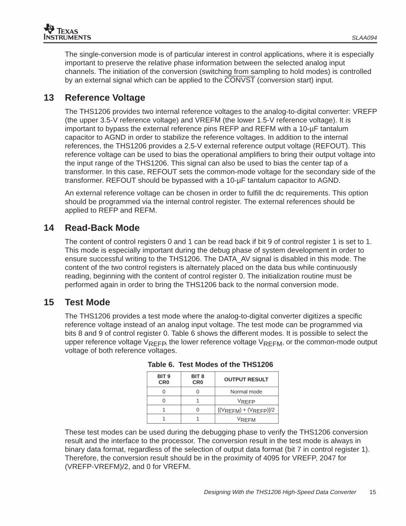
15 Test ModeThe THS1206 provides a test mode where the analog-to-digital converter digitizes a specificreference voltage instead of an analog input voltage. The test mode can be programmed viabits 8 and 9 of control register 0. Table 6 shows the different modes. It is possible to select theupper reference voltage VREFP, the lower reference voltage VREFM, or the common-mode outputvoltage of both reference voltages.
Table 6. Test Modes of the THS1206
BIT 9CR0
BIT 8CR0 OUTPUT RESULT
0 0 Normal mode
0 1 VREFP
1 0 [(VREFM) + (VREFP)]/2
1 1 VREFM
These test modes can be used during the debugging phase to verify the THS1206 conversionresult and the interface to the processor. The conversion result in the test mode is always inbinary data format, regardless of the selection of output data format (bit 7 in control register 1).Therefore, the conversion result should be in the proximity of 4095 for VREFP, 2047 for(VREFP-VREFM)/2, and 0 for VREFM.
SLAA094
16 Designing With the THS1206 High-Speed Data Converter
The conversion is based on the reference voltage selected: either internal or external. Thisoption must be configured via the internal control register.
The DATA_AV signal is disabled in this test mode. This means that the conversion value of thetest voltage can be read from the processor independent of any control signal. However, thismeans that in the test mode the DATA_AV signal can not be used as a control signal to causethe processor to jump to an interrupt service routine.
16 Overflow FlagAn overflow flag set to 1 indicates that the FIFO data was overwritten before the processor wasable to read it. This feature can be useful during debugging and development phases were theprocessor software must be tested. Such tests can be conducted as indicated in the followingexample. The application demands the processing of 4,096 digital values. It must be ensuredthat FIFO overflow does not occur during the conversion process. The overflow condition can bechecked immediately after the 4,096 values have been read in order to ensure that theprocessor is sufficiently fast to read all the data. The THS1206 should be programmed into theread-back mode to read the overflow bit. Since the conversion clock is still running, theprocedure must be sufficiently fast to prevent an overflow during the test. The initializationroutine should be performed again to bring the THS1206 back to normal conversion mode. Theoverflow flag is set back to 0 during the initialization routine.
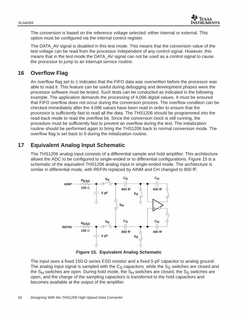
17 Equivalent Analog Input SchematicThe THS1206 analog input consists of a differential sample and hold amplifier. This architectureallows the ADC to be configured to single-ended or to differential configurations. Figure 15 is aschematic of the equivalent THS1206 analog input in single-ended mode. The architecture issimilar in differential mode, with REFIN replaced by AINM and CH changed to 800 fF.
_
+
CH
400 fF
CH
CS
800 fFSS
CS
SS
SH
SS
SS
5 pF
5 pF
RESD
150 Ω
RESD
150 Ω
AINP
REFIN400 fF800 fF
Figure 15. Equivalent Analog Schematic
The input sees a fixed 150-Ω series ESD resistor and a fixed 5-pF capacitor to analog ground.The analog input signal is sampled with the CS capacitors, while the SS switches are closed andthe SH switches are open. During hold mode, the SH switches are closed, the SS switches areopen, and the charge of the sampling capacitors is transferred to the hold capacitors andbecomes available at the output of the amplifier.

SLAA094
17 Designing With the THS1206 High-Speed Data Converter
18 Analog Input ConfigurationThe THS1206 features four analog input channels. These channels can be configured for eithersingle-ended or differential operation. Figure 16 shows a simplified model with a single-endedconfiguration selected for channel AINP. The reference voltages for the ADC itself are VREFPand VREFM (either internal or external reference voltages). The analog input voltage ranges fromVREFM to VREFP. This means that VREFM defines the minimum voltage, and VREFP defines themaximum voltage that can be applied to the ADC. The internal reference source provides thevoltage VREFM of 1.5 V and the voltage VREFP of 3.5 V (see the Reference Voltage section). Theresulting analog input voltage swing of 2 V can be expressed by:
VREFM AINP VREFP
12-BitADC
VREFP
VREFM
AINP
Figure 16. Single-Ended Input Stage
In many applications a differential operation is required to attain a better signal-to-noise ratio.Figure 17 shows a simplified model of analog inputs AINM and AINP, which are configured fordifferential operation. The differential mode is recommended because it offers benefits inperformance over the single-ended mode. However, the THS1206 offers two differential analoginputs in this mode, while the single-ended mode offers four analog inputs. Common-modenoise and common-mode voltages can be rejected using a differential analog input architecture.Further details on both modes are given below.
12-BitADC
VREFP
VREFM
AINP
ΣVADC
AINM
+
-
Figure 17. Differential Input Stage
In contrast to the single-ended configuration, it can be seen that the voltage VADC applied at theinput of the ADC is the difference between the AINP and AINM inputs. The voltage VADC can becalculated as follows:
VADC |AINP AINM|
The advantage of single-ended operation is that the common-mode voltage:
VCMAINM AINP
2
can be rejected in the differential configuration if the analog input satisfies the followingconditions:
(1)
(2)
(3)

SLAA094
18 Designing With the THS1206 High-Speed Data Converter
AGND AINM, AINP AVDD
1 V VCM 4 V
18.1 Single-Ended Mode
The THS1206 can be configured for single-ended operation using dc or ac coupling. In eithercase the THS1206 input should be driven by an operational amplifier that does not degrade theperformance of its ADC. Because the THS1206 operates from a single 5-V supply, it isnecessary to level-shift ground-based bipolar signals to comply with its input requirements. Thiscan be achieved with dc and ac couplings. Application examples will be shown for bothmethods.
18.2 DC Coupling
An operational amplifier can be configured to shift the signal level according to the THS1206analog input voltage range. This voltage range extends from 1.5 V to 3.5 V. An op amp can beused as shown in Figure 18.
_
+
5 VR1
51 Ω
3.5 V2.5 V1.5 V
THS1206
AINP
REFOUT
R2
1.25 V
1 V0 V
–1 VTHS4011/THS4031/THS4051
–5 V
R1
REFIN
10 µF+
R2
1 nF
Figure 18. Level Shift for DC-Coupled Input
Figure 18 shows an application example where an analog input signal range of –1-V to 1-V isshifted by an op amp to the analog input range of the THS1206 (1.5 V to 3.5 V). The op amp isconfigured as an inverting amplifier with a gain of –1. The required 1.25 Vdc voltage at thenoninverting input is derived from the THS1206’s 2.5-V output reference REFOUT by using aresistor divider. Therefore, the op amp output voltage will be centered at 2.5 V. The 10-µFtantalum capacitor is required to bypass REFOUT. REFIN should be directly connected toREFOUT in single-ended mode. The use of ratio-matched, thin-film resistor networks minimizesgain and offset errors. A resistor value of 10 kΩ is recommended, since REFOUT is capable ofdelivering 250 µA. The RC filter (with R = 51 Ω and C = 1 nF) at the output of the op ampimproves the THS1206 dynamic performance.
Texas Instruments provides a wide range of high speed operational amplifiers which best fit theTHS1206. The THS4051 is an excellent choice for high-speed applications. It has a high slewrate of 200 V/µs and an extremely-low distortion of only –87 dB at ± 5-V supply voltage. Forhigher dc precision requirements, the THS4031 is a good choice with its maximum input offsetvoltage of only 2 mV. Other parameters include an extremely low distortion of –90 dB and a slewrate of 80 V/µs at ± 5-V supply voltage.
(4)
(5)

SLAA094
19 Designing With the THS1206 High-Speed Data Converter
18.3 AC-Coupled Input
Figure 19 shows an analog input ac-coupled to the THS1206. Capacitor C1 is placed in serieswith the input of the op amp for ac-coupling. The analog signal is shifted by biasing thenoninverting input of the amplifier with the THS1206’s REFOUT signal.
_
+
5 V
R
R51 Ω
3.5 V2.5 V1.5 V
THS1206
AINP
1 V0 V
–1 V
THS4011/THS4031/THS4051
–5 V
100 nF1 nF
C1
REFIN
REFOUT
+10 µF
Figure 19. AC-Coupled Input
18.4 Differential Mode
In the differential mode of operation, a differential analog signal is applied to the differential inputof the THS1206. A conversion from a single ended to a differential signal is required in mostcases. This can be achieved in different ways: using two operational amplifiers configured toprovide a differential output, or using an operational amplifier to provide a differential input aswell as a differential output.
An RF transformer with a center tap on the secondary side provides an alternative to theoperational amplifier. The use of the RF transformer is advantageous at the higher frequenciesin terms of total harmonic distortion (THD) and spurious free dynamic range (SFDR). The centertap of the transformer can be used to shift the differential signal to the common-mode levelrequired. In contrast to the operational amplifier, the analog signal is ac-coupled automaticallywhen using an RF-transformer.
Figure 20 shows an RF-transformer used to generate a differential signal from a single-endedsignal. The center tap of the secondary is connected to REFOUT of the THS1206. Therefore,the common-mode level of the analog signal is tied to REFOUT, which is 2.5 V. The RC filter(with R = 51 Ω and C = 1 nF) in front of the analog input of the THS1206 op amp improves thenoise performance.
THS1206
AINP
AINM
REFOUT
1 nF
51 Ω200 Ω
49.9 Ω
MinicircuitsT4-1
51 Ω
1 nF
Figure 20. Single-Ended to Differential Conversion by Transformer

SLAA094
20 Designing With the THS1206 High-Speed Data Converter
19 Layout Considerations
The layout of a mixed signal design must fulfill the digital and analog signal requirements. Inpurely digital systems, the signals to be transmitted from one point (device) to the other aresolely high- and low-levels. Very fast edges (up to 200 ps/V) can occur with high-speed devices.These fast edges cause very high current spikes on the supply voltage. In analog systems it ismost important to transceive signals without distortion, noise, ripple, or crosstalk. In mixed signalsystems the challenge is to avoid coupling from the noisy digital portion to the sensitive analogarea, especially with the increasing processor clock rates. The analog portion must bedecoupled from the digital portion. Using the THS1206 as an example, the weight of one LSB(least significant bit) in the single-ended mode is less than 500 µV, indicating that anyinterference from the processor can easily exceed this value. It becomes especially important toreview some of the basic rules in order to make the analog side of a mixed signal design lesssensitive to any digital activity in the system.
The mixed signal design requires the use of a multilayer board to minimize the influence of thenoisy digital part into the analog part, especially at higher speed and resolution. Figure 21 showsan example of a four-layer board. The multilayer board allows for separation of the analog anddigital sections of the system.
Analog Signal Lines
Analog Ground Plane
Analog Supply Voltages
Analog Signal Lines
Digital Signal Lines
Digital Ground Plane
Digital Supply Voltages
Digital Signal Lines
Distance BetweenGround PlanesLayer 1
Layer 4
Figure 21. Mixed-Signal Four-Layer Board
The second layer provides separate analog and digital ground planes. The first and fourth layersare used for the analog and digital signal lines. The analog signal lines are laid over the analogground plane, and the digital signal lines are laid over the digital ground plane. The analogsignal lines should be as short as possible, not too dense, and parallel to other lines. The areabetween signal lines can be filled by extending the ground area connected to the ground plane.This provides further shielding and reduces the sensitivity to coupling and crosstalk, especiallyimportant with analog signals. The third layer provides the analog and digital supply voltages.The two adjacent ground and supply line planes form an extremely-low inductive decouplingcapacitor. This design results in the best decoupling between analog and digital signal lines.
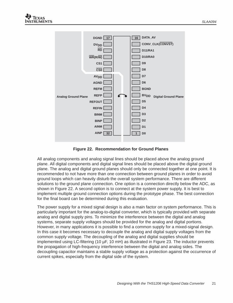
Figure 22 illustrates the recommendations for ground-plane splitting on the THS1206. Splitting ofthe ground plane is done directly below the THS1206 so that all digital pins are beyond thedigital ground plane, and the analog pins are beyond the analog ground plane. The splitbetween ground planes should be separated by at least 3 mm to minimize the capacitancebetween these planes.
SLAA094
21 Designing With the THS1206 High-Speed Data Converter
32
17
1
16DGND
DVDD
RD
WR(R/W)
CS1
CS0
AVDD
AGND
REFM
REFP
REFOUT
REFIN
BINM
BINP
AINM
AINP
DATA_AV
CONV_CLK(CONVST)
D11/RA1
D10/RA0
D9
D8
D7
D6
BGND
BVDD
D5
D4
D3
D2
D1
D0
Analog Ground Plane Digital Ground Plane
Figure 22. Recommendation for Ground Planes
All analog components and analog signal lines should be placed above the analog groundplane. All digital components and digital signal lines should be placed above the digital groundplane. The analog and digital ground planes should only be connected together at one point. It isrecommended to not have more than one connection between ground planes in order to avoidground loops which can heavily disturb the overall system performance. There are differentsolutions to the ground plane connection. One option is a connection directly below the ADC, asshown in Figure 22. A second option is to connect at the system power supply. It is best toimplement multiple ground connection options during the prototype phase. The best connectionfor the final board can be determined during this evaluation.
The power supply for a mixed signal design is also a main factor on system performance. This isparticularly important for the analog-to-digital converter, which is typically provided with separateanalog and digital supply pins. To minimize the interference between the digital and analogsystems, separate supply voltages should be provided for the analog and digital portions.However, in many applications it is possible to find a common supply for a mixed-signal design.In this case it becomes necessary to decouple the analog and digital supply voltages from thecommon supply voltage. The decoupling of the analog and digital supplies should beimplemented using LC-filtering (10 µF, 10 mH) as illustrated in Figure 23. The inductor preventsthe propagation of high-frequency interference between the digital and analog sides. Thedecoupling capacitor maintains a stable supply voltage as a protection against the occurrence ofcurrent spikes, especially from the digital side of the system.

SLAA094
22 Designing With the THS1206 High-Speed Data Converter
+ +
Ld La
Cd Ca
AVDDDVDD
Supply Voltage
Figure 23. Common Supply for a Mixed Signal Design
The THS1206 provides separate supply pins for the analog side (AVDD, AGND), for the digitalside (DVDD, DGND), and for the buffer unit (BVDD, BGND) of the device. The buffer has its ownsupply pins to minimize noise interference to the sensitive analog area during switching of therelatively-strong buffer. AVDD should come from the analog supply, and DVDD and BVDD shouldcome from the digital supply. Every supply should have its own decoupling. This filtering is veryimportant because the digital supply for the THS1206 comes from the common digital supplyvoltage.
The analog portion of the THS1206 should be decoupled from the noisy digital supply voltage.This is typically done by using a 10-µF tantalum capacitor in parallel with a 100-nF ceramiccapacitor. The tantalum capacitor takes care of the lower-frequency disturbing components,while the ceramic capacitor takes care of the higher-frequency disturbing components. Newtantalum capacitors are available with similarly good behavior at both low and high frequencies(for example, the Siemens B45196E3106). The use of a ceramic capacitor in parallel with atantalum capacitor has now become unnecessary. In addition to the capacitor, a 10-µH inductorshould be used to provide further filtering. This bypassing example is shown in Figure 24. Thebypass capacitors should be placed as close as possible to the THS1206 supply pins.
+
THS1206
AVDD
AGND
DVDD
DGND
+10 µF
AGND
10 µH 10 µHAVDD DVDD
BVDD
BGND
+
10 µH
10 µF
10 µF
DGND
DGND
Figure 24. Use of Bypassing With The THS1206
Siemens is a trademark of Siemens Components, Inc.
SLAA094
23 Designing With the THS1206 High-Speed Data Converter
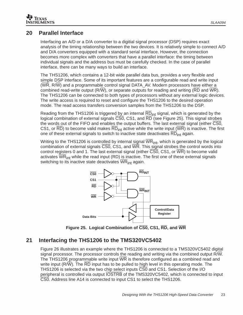
20 Parallel Interface
Interfacing an A/D or a D/A converter to a digitial signal processor (DSP) requires exactanalysis of the timing relationship between the two devices. It is relatively simple to connect A/Dand D/A converters equipped with a standard serial interface. However, the connectionbecomes more complex with converters that have a parallel interface: the timing betweenindividual signals and the address bus must be carefully checked. In the case of parallelinterface, there can be many ways to build an interface.
The THS1206, which contains a 12-bit wide parallel data bus, provides a very flexible andsimple DSP interface. Some of its important features are a configurable read and write input(WR, R/W) and a programmable control signal DATA_AV. Modern processors have either acombined read-write output (R/W), or separate outputs for reading and writing (RD and WR).The THS1206 can be connected to both types of processors without any external logic devices.The write access is required to reset and configure the THS1206 to the desired operationmode. The read access transfers conversion samples from the THS1206 to the DSP.
Reading from the THS1206 is triggered by an internal RDint signal, which is generated by thelogical combination of external signals CS0, CS1, and RD (see Figure 25). This signal strobesthe words out of the FIFO and enables the output buffers. The last external signal (either CS0,CS1, or RD) to become valid makes RDint active while the write input (WR) is inactive. The firstone of these external signals to switch to inactive state deactivates RDint again.
Writing to the THS1206 is controlled by internal signal WRint, which is generated by the logicalcombination of external signals CS0, CS1, and WR. This signal strobes the control words intocontrol registers 0 and 1. The last external signal (either CS0, CS1, or WR) to become validactivates WRint while the read input (RD) is inactive. The first one of these external signalsswitching to its inactive state deactivates WRint again.
RDINT
WRINT
Control/DataRegister
CS0
CS1
RD
WR
Data Bits
Figure 25. Logical Combination of CS0 , CS1, RD, and WR
21 Interfacing the THS1206 to the TMS320VC5402
Figure 26 illustrates an example where the THS1206 is connected to a TMS320VC5402 digitalsignal processor. The processor controls the reading and writing via the combined output R/W.The THS1206 programmable write input WR is therefore configured as a combined read andwrite input (R/W). The RD input has to be pulled to high level in this operating mode. TheTHS1206 is selected via the two chip select inputs CS0 and CS1. Selection of the I/Operipheral is controlled via output IOSTRB of the TMS320VC5402, which is connected to inputCS0. Address line A14 is connected to input CS1 to select the THS1206.

SLAA094
24 Designing With the THS1206 High-Speed Data Converter
IOSTRB
A14
R/W
INTX
BCLKX
DATA
TMS320VC5402
12
CS0
CS1
R/W
DATA_AV
CONV_CLK
DATA
RD
AINP
AINM
BINP
BINM
4.7 kΩ
DVDD
AIN 1
AIN 2
AIN 3
AIN 4
THS1206
Figure 26. Interfacing the THS2106 to the TMS320VC5402
The THS1206 data bus (D0–D11) is directly connected to the TMS320VC5402 data bus. D0–D11of the THS1206 can be connected to the lower data bits D0–D11 or to the higher data bits D4–D15of the TMS320VC5402. This choice should be application dependent. In this example, theconversion clock is generated by the TMS320VC5402 serial port. Signal BCLKX can beprogrammed to provide a clock signal with a 50% duty cycle. To attain the best dynamic performaceit is recommended to use a low-jitter external clock source. The clock source jitter has a significantimpact on noise performance. The converted data is read by the TMS320VC5402 and thentriggered via an interrupt (INTX) connected to DATA_AV.
Figure 27 shows the timing diagram for a write to the THS1206 based on the interface shown inFigure 26. The data is latched into the THS1206 with the rising edge of IOSTRB. The datasetup (tsu) and hold time (th) of the THS1206 have to be aligned with the timing for a parallel I/Oport write of the TMS320VC5402.
ÎÎÎÎÎÎ
ÏÏÏÏÏÏ
10% 10%90%
tWCS
tsu(R/W) th(R/W)
tsu th
90%90%
CS0 (IOSTRB)
CS1 (A14)
R/W
RD
D[11:0]
10% 10%
Figure 27. Write Access to the THS1206 (CS0 -IOSTRB-Controlled)
If the setup time for the processor data is too small, the timing between peripheral andprocessor must be adjusted. This adjustment is done from the TMS320VC5402 byprogramming of internal wait states.
SLAA094
25 Designing With the THS1206 High-Speed Data Converter
ÎÎÎÎÎÎ
ÏÏÏÏÏÏ
10% 10%90%
tWCS
tsu(RD) th(RD)
th
90%90%
CS0 (IOSTRB)
CS1 (A14)
R/W
RD
D[11:0]
10% 10%
ta
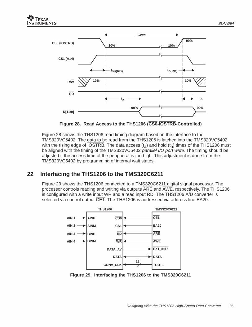
Figure 28. Read Access to the THS1206 (CS0 -IOSTRB-Controlled)
Figure 28 shows the THS1206 read timing diagram based on the interface to theTMS320VC5402. The data to be read from the THS1206 is latched into the TMS320VC5402with the rising edge of IOSTRB. The data access (ta) and hold (th) times of the THS1206 mustbe aligned with the timing of the TMS320VC5402 parallel I/O port write. The timing should beadjusted if the access time of the peripheral is too high. This adjustment is done from theTMS320VC5402 by programming of internal wait states.
22 Interfacing the THS1206 to the TMS320C6211
Figure 29 shows the THS1206 connected to a TMS320C6211 digital signal processor. Theprocessor controls reading and writing via outputs ARE and AWE, respectively. The THS1206is configured with a write input WR and a read input RD. The THS1206 A/D converter isselected via control output CE1. The THS1206 is addressed via address line EA20.
CE1
EA20
ARE
AWE
EXT_INT6
DATA
TMS320C6211
12
CS0
CS1
WR
DATA_AV
CONV_CLK
DATA
AINP
AINM
BINP
BINM
AIN 1
AIN 2
AIN 3
AIN 4
THS1206
RD
TOUT1
Figure 29. Interfacing the THS1206 to the TMS320C6211

SLAA094
26 Designing With the THS1206 High-Speed Data Converter
The THS1206 data bus (D0–D11) is directly connected to the TMS320C6211 data bus. In thisexample, the conversion clock is generated by timer1, which can be configured to provide aclock signal with a 50% duty cycle. The use of a low-jitter external clock source isrecommended to attain the best dynamic performance. Clock source jitter has a significantimpact on noise performance. The converted data is read by the TMS320C6211 under controlof an interrupt (EXT_INT6) connected to DATA_AV.
tw(WR)
10% 10%
tsu th
90% 90%
CS0 (CE1)
CS1 (EA20)
WR (AWE)
RD (ARE)
D [11:0]
Figure 30. Write Access to the THS1206 (WR -AWE-Controlled)
Figure 30 shows the THS1206 write timing diagram for an interface to the TMS320C6211. Thedata is latched into the THS1206 with the rising edge of AWE. The THS1206 data setup (tsu)and hold (th) times must be compared with the asynchronous memory write timing of theTMS320C6211. If the setup and hold times for the TMS320C6211 data are too small, the timingbetween the peripheral and the processor should be adjusted. This adjustment can be doneeasily on the TMS320C6211 by programming of internal wait states for the setup and for thehold times.

SLAA094
27 Designing With the THS1206 High-Speed Data Converter
ÏÏÏÏÏÏÏÏÏÏÏÏ
ÎÎÎÎÎÎÎÎÎÎÎÎ
tsu(CS) th(CS)
tw(RD)
ta th
90% 90%
10% 10%90%
90%90%
CS0 (CE1)
CS1 (EA20)
WR (AWE)
RD (ARE)
D (11–0)
Figure 31. Read Access to the THS1206 (RD -ARE-Controlled)
Figure 31 shows the read timing diagram of the THS1206 based on an interface to theTMS320C6211. The data to be read from the THS1206 is latched into the TMS320C6211 withthe rising edge of ARE. The data access (ta) and hold time (th) of the THS1206 should bealigned with the TMS320C6211 asynchronous memory read timing. If the access time of theperipheral is too high, the timing should be adjusted. This adjustment is done from theTMS320C6211 by programming of internal wait states.
23 Summary
This application report describes the criteria applied in designing a system using the THS1206high-speed data converter. The THS1206, with its 12-bit data bus and 6-MSPS conversion rate,is an analog-to-digital converter especially designed to operate with digital signal processors(DSP). The THS1206 features make it especially attractive in radar, high-speed dataacquisition, communications, and control applications. The main features of the THS1206 areits four analog inputs which can be switched from sampling to hold mode simultaneously and itsintegrated FIFO which incresases the maximum data throughput between ADC and processor.
The report explains the initialization and operation of the THS1206. Two examples show theTHS1206 connected to digital signal processors TMS320VC5402 and TMS320C6201. A dis-cussion on different options to drive the analog input of the THS1206 is also included. Layoutconsiderations offer hints on achieving the best system performance.

SLAA094
28 Designing With the THS1206 High-Speed Data Converter
24 References1. Texas Instruments, THS1206 data sheet, literature number SLAS217C
2. Texas Instruments, Data Acquisition Circuits data sheet, literature number SLAD001A
3. Texas Instruments, TMS320C6211 data sheet, literature number SPRS073A
4. Texas Instruments, TMS320VC5402 data sheet, literature number SPRS079D
5. Texas Instruments, Analog Applications, literature number SLYT005
6. Texas Instruments, Analog Applications Journal, literature number SLYT010
7. Texas Instruments, Electrostatic Discharge application note, literature number SSYA008
8. Texas Instruments, Selecting an Amplifier for a Data Converter, literature number SLOA035
9. Texas Instruments, Linear Design Seminar 1999, literature number SLYD016
25 Glossary
AC Alternating currentADC Analog-to-digital converterDC Direct currentDSP Digital signal processorFIFO Firt-in first-outRF Radio frequencySFDR Spurious free dynamic rangeTHD Total harmonic distorsionTL Trigger level

IMPORTANT NOTICE
Texas Instruments and its subsidiaries (TI) reserve the right to make changes to their products or to discontinueany product or service without notice, and advise customers to obtain the latest version of relevant informationto verify, before placing orders, that information being relied on is current and complete. All products are soldsubject to the terms and conditions of sale supplied at the time of order acknowledgment, including thosepertaining to warranty, patent infringement, and limitation of liability.
TI warrants performance of its semiconductor products to the specifications applicable at the time of sale inaccordance with TI’s standard warranty. Testing and other quality control techniques are utilized to the extentTI deems necessary to support this warranty. Specific testing of all parameters of each device is not necessarilyperformed, except those mandated by government requirements.
Customers are responsible for their applications using TI components.
In order to minimize risks associated with the customer’s applications, adequate design and operatingsafeguards must be provided by the customer to minimize inherent or procedural hazards.
TI assumes no liability for applications assistance or customer product design. TI does not warrant or representthat any license, either express or implied, is granted under any patent right, copyright, mask work right, or otherintellectual property right of TI covering or relating to any combination, machine, or process in which suchsemiconductor products or services might be or are used. TI’s publication of information regarding any thirdparty’s products or services does not constitute TI’s approval, warranty or endorsement thereof.
Copyright 2000, Texas Instruments Incorporated