Designandimplementation ofaDDS-basedmulti-carrier … · Designandimplementation...
17
INTERNATIONAL JOURNAL OF COMMUNICATION SYSTEMS Int. J. Commun. Syst. (2009) Published online in Wiley InterScience (www.interscience.wiley.com). DOI: 10.1002/dac.1014 Design and implementation of a DDS-based multi-carrier GMSK modulator M. J. Kesoulis 1 , C. S. Koukourlis 1,∗, † , J. N. Lygouras 1 , D. Soudris 1 and J. N. Sahalos 2 1 Department of Electrical and Computer Engineering, Democritus University of Thrace, Xanthi GR-67100, Greece 2 Radiocommunications Laboratory, Department of Physics, Aristotle University of Thessaloniki, Thessaloniki GR-54124, Greece SUMMARY The design and hardware implementation of a multi-carrier Gaussian minimum shift keying (GMSK) modulator, based on a direct digital synthesizer, suitable for global system for mobile (GSM) base station applications is described. The synthesizer does not only generate the baseband GMSK signal, but also delivers it at a low IF. Special care has been taken in order to minimize the required memory of the synthe- sizer. The hardware implementation is mainly based on a field programmable gate array device (FPGA) and a D/A converter. The number of carriers depends on the size of the FPGA. Finally, the hardware implementation of a two-carrier modulator is given. Copyright 2009 John Wiley & Sons, Ltd. Received 14 March 2008; Accepted 15 February 2009 KEY WORDS: GSM; GMSK modulation; Direct Digital Synthesis (DDS); Gaussian filter 1. INTRODUCTION Gaussian minimum shift keying (GMSK) is a well-known modulation scheme since it was adopted for the second generation of European mobile telephony standard, global system for mobile (GSM). A common practice in mobile communications base stations is to multiplex the power amplifier outputs of several frequency channels just on the transmitting antenna. Combiners are implemented to use the same antenna for several carriers. The more the carriers are combined, the greater the combiner loss appears. Up to 8:1 combiners are found to be in use in micro and pico cells. The multiplexing (combining) technique affects the spectrum usage. Spectrum is a finite and costly resource to an operator. Making optimum use provides the best possible customer service ∗ Correspondence to: C. S. Koukourlis, Department of Electrical and Computer Engineering, Democritus University of Thrace, Xanthi GR-67100, Greece. † E-mail: [email protected] Copyright 2009 John Wiley & Sons, Ltd.
Transcript of Designandimplementation ofaDDS-basedmulti-carrier … · Designandimplementation...
INTERNATIONAL JOURNAL OF COMMUNICATION SYSTEMSInt. J. Commun. Syst. (2009)Published online in Wiley InterScience (www.interscience.wiley.com). DOI: 10.1002/dac.1014
Design and implementation of a DDS-based multi-carrierGMSKmodulator
M. J. Kesoulis1, C. S. Koukourlis1,∗,†, J. N. Lygouras1, D. Soudris1 and J. N. Sahalos2
1Department of Electrical and Computer Engineering, Democritus University of Thrace,Xanthi GR-67100, Greece
2Radiocommunications Laboratory, Department of Physics, Aristotle University of Thessaloniki,Thessaloniki GR-54124, Greece
SUMMARY
The design and hardware implementation of a multi-carrier Gaussian minimum shift keying (GMSK)modulator, based on a direct digital synthesizer, suitable for global system for mobile (GSM) base stationapplications is described. The synthesizer does not only generate the baseband GMSK signal, but alsodelivers it at a low IF. Special care has been taken in order to minimize the required memory of the synthe-sizer. The hardware implementation is mainly based on a field programmable gate array device (FPGA)and a D/A converter. The number of carriers depends on the size of the FPGA. Finally, the hardwareimplementation of a two-carrier modulator is given. Copyright q 2009 John Wiley & Sons, Ltd.
Received 14 March 2008; Accepted 15 February 2009
KEY WORDS: GSM; GMSK modulation; Direct Digital Synthesis (DDS); Gaussian filter
1. INTRODUCTION
Gaussian minimum shift keying (GMSK) is a well-known modulation scheme since it was adoptedfor the second generation of European mobile telephony standard, global system for mobile (GSM).A common practice in mobile communications base stations is to multiplex the power amplifieroutputs of several frequency channels just on the transmitting antenna. Combiners are implementedto use the same antenna for several carriers. The more the carriers are combined, the greater thecombiner loss appears. Up to 8:1 combiners are found to be in use in micro and pico cells.
The multiplexing (combining) technique affects the spectrum usage. Spectrum is a finite andcostly resource to an operator. Making optimum use provides the best possible customer service
∗Correspondence to: C. S. Koukourlis, Department of Electrical and Computer Engineering, Democritus Universityof Thrace, Xanthi GR-67100, Greece.
†E-mail: [email protected]
Copyright q 2009 John Wiley & Sons, Ltd.
M. J. KESOULIS ET AL.
at the lowest cost. The optimum spectrum usage depends on the ability to assign the spectrumflexibly, which is feasible when somebody has the total freedom of deploying channels across abase station network. Early base stations used selective cavity combiners that sum the transmitsignals to the antenna feeder. The combining process wasted a relatively little amount of the RFtransmitter power. However, it was inflexible in terms of the carriers that could be deployed at agiven base site. Generally, a 5–10 carrier ‘dead zone’ existed on either side of a deployed carrierin a typical GSM cell-site installation. Recently, lossy passive combiners have been employed inbase station designs. The latter overcome the frequency allocation restrictions of cavity combiners,which means a high price in terms of cell-site efficiency and, hence, materialization cost.
The purpose of this paper is not only to give another implementation of the modulation, butalso to provide a technique according to which the multiplexing takes place at an earlier stage, i.e.the multiplexed signal is generated directly at the output of a digital-to-analog converter (DAC),which is the final building block of a direct digital synthesizer (DDS) stage. In addition, thechannel allocation is provided efficiently by the use of appropriate channel frequency setting words(FSWC). The described implementation of the GMSK modulator is referred only for GSM basestation applications since multiplexing of frequency channels is meaningless for hand-held devices.Thus, the size or the power consumption is not considered as major aspects. The proposed designis based on commercially available chips for the major parts, i.e. the field programmable gate array(FPGA) and the DAC, leading to short time to the market solutions. In addition, in contrast toASIC implementations, the programmability of the FPGA provides the flexibility of fast circuitrychanges. One of the main characteristics of our design is that several stages of the synthesizer,including the DAC are common for all the composed frequency channels.
A very interesting approach in multi-carrier modulation is given in [1, 2]. In the above, fourDDS-based GMSK modulators, combined in the digital domain, drive a common D/A converter.Our approach differs to [1, 2] because not only the final D/A converter but also the whole DDSand the Gaussian filter are shared among all the frequency channels. Combining the carriers in thetime domain aims at the reduction of the large number of analog components that are requiredfor the traditional implementations. The problem that arises is that if a common nonlinear poweramplifier is to be used, this will give rise to intermodulation products and to spectral growth. Thisis in contrast to the basic property of GMSK, single channel modulation, where a constant envelopeexists. This problem can be bypassed by linearization of the operation of the above amplifier.
2. GMSK MODULATION
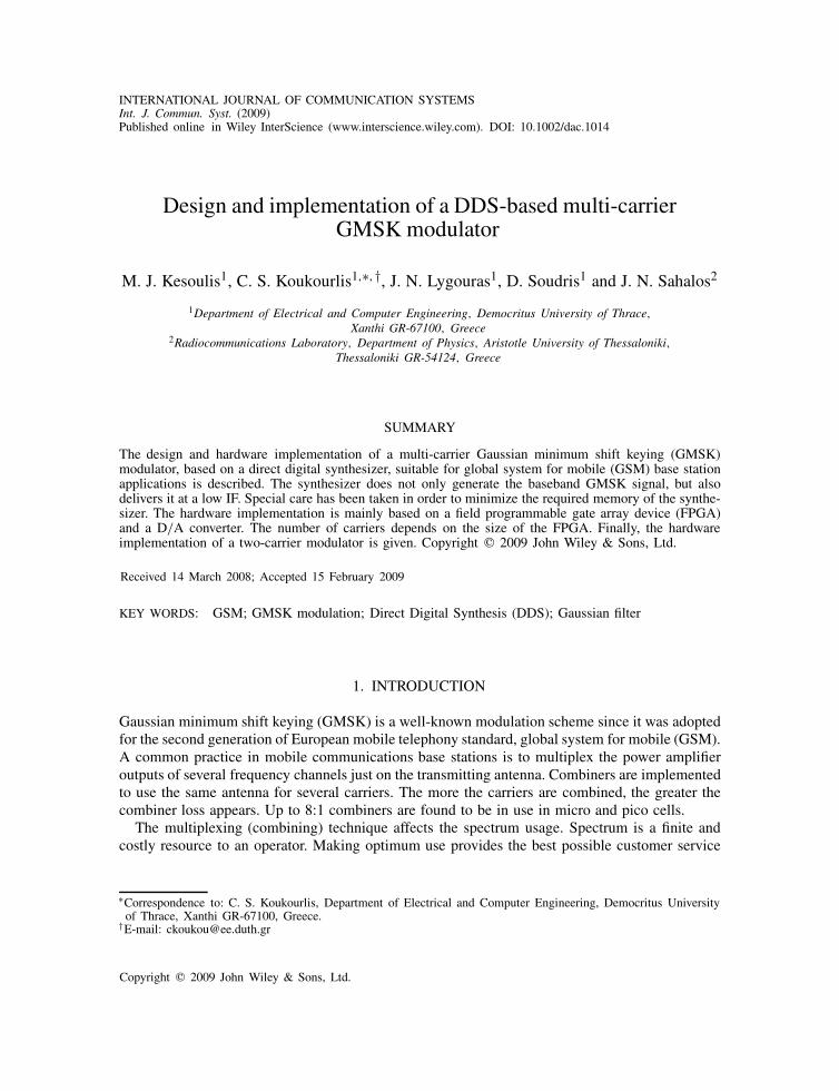
It is well known that GMSK modulation has been proposed a long time ago [3] and since thenseveral implementations took place. The ‘analog’ approach, shown in Figure 1, for generating aGMSK signal is the ‘Gaussian’ filtering of the incoming data and next their entry to a frequencymodulator, i.e. a voltage controlled oscillator (VCO). If the input data are suitably Gaussian pre-filtered (bell shaped) and then are applied to the MSK modulator, GMSK modulation results,(Figure 1). In the present paper a digital implementation is described where a DDS replaces theVCO, and a look-up table replaces the Gaussian filter [4]. In an all-analog implementation, theVCO is driven by the filtered version of the data waveform. Instead, in the DDS case, a sequence ofFSW has to be supplied in an appropriate manner to the DDS input in order to ensure the generationof GMSK waveform. Additional advantages of the mostly digital implementation with the use ofa DDS [1, 2] instead of an I/Q modulator is the saving of large number of analog components
Copyright q 2009 John Wiley & Sons, Ltd. Int. J. Commun. Syst. (2009)DOI: 10.1002/dac
DDS-BASED MULTI-CARRIER GMSK MODULATOR
FM (MSK) TRANSMITTER
or VCO
PREMODULATIONGAUSSIAN
FILTER
GAIN k
Modulated Carrier
TX Data Input
Figure 1. GMSK transmitting system.
many of which require production tuning and lead to reduced accuracy of implementation overthe digital one. Also there is no need of adjustments of dc offset and amplitude levels as in I/Qmodulator.
It is well known that the Gaussian filter in GSM needs a normalized bandwidth BT =0.3(bandwidth and symbol time product), which prevents the intersymbol interference (ISI). It hasbeen shown [5] that for ISI evaluation it is enough to take into account only the interference oftwo neighboring bits. Each one of them lies at each side of the currently processed bit. In Figure 1the gain k ensures a modulation index � of exactly 1
2 [6, 7].
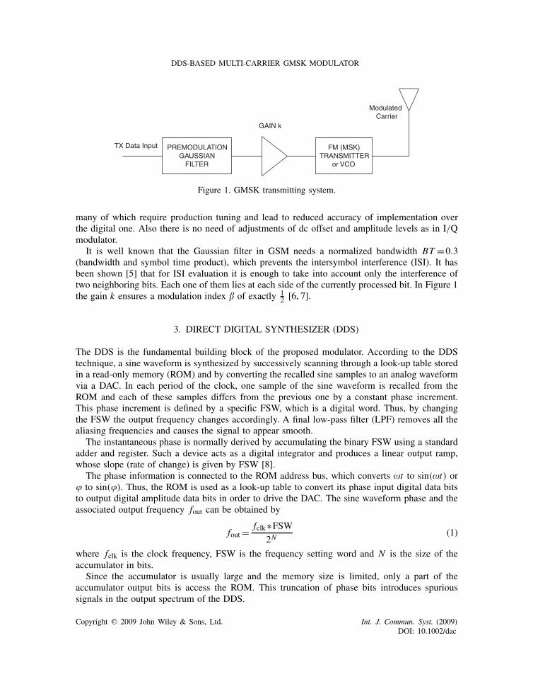
3. DIRECT DIGITAL SYNTHESIZER (DDS)
The DDS is the fundamental building block of the proposed modulator. According to the DDStechnique, a sine waveform is synthesized by successively scanning through a look-up table storedin a read-only memory (ROM) and by converting the recalled sine samples to an analog waveformvia a DAC. In each period of the clock, one sample of the sine waveform is recalled from theROM and each of these samples differs from the previous one by a constant phase increment.This phase increment is defined by a specific FSW, which is a digital word. Thus, by changingthe FSW the output frequency changes accordingly. A final low-pass filter (LPF) removes all thealiasing frequencies and causes the signal to appear smooth.
The instantaneous phase is normally derived by accumulating the binary FSW using a standardadder and register. Such a device acts as a digital integrator and produces a linear output ramp,whose slope (rate of change) is given by FSW [8].
The phase information is connected to the ROM address bus, which converts �t to sin(�t) or� to sin(�). Thus, the ROM is used as a look-up table to convert its phase input digital data bitsto output digital amplitude data bits in order to drive the DAC. The sine waveform phase and theassociated output frequency fout can be obtained by
fout= fclk∗FSW2N
(1)
where fclk is the clock frequency, FSW is the frequency setting word and N is the size of theaccumulator in bits.
Since the accumulator is usually large and the memory size is limited, only a part of theaccumulator output bits is access the ROM. This truncation of phase bits introduces spurioussignals in the output spectrum of the DDS.
Copyright q 2009 John Wiley & Sons, Ltd. Int. J. Commun. Syst. (2009)DOI: 10.1002/dac
M. J. KESOULIS ET AL.
W
x
L
MFine
Rom
Coarse
RomB
A
C
A
XOR
XOR ShiftReg
g(x)
D
Additional
logic
W-5
W-3
W-2
q(x)
W-4
XOR XOR(1)
x/4
N
Acc
umul
ator
fclk
Figure 2. Block diagram of the DDS.
In this paper, a technique developed in [9] is adopted for implementing the DDS. This techniqueexploits certain properties of the existing algorithms and modifies them properly, achieving bettercompression ratios of ROM.
The basic concept of this method (Figure 2) is the generation of an auxiliary function f (x),easily implemented concerning the hardware complexity, which approximates the sine waveformin a closer level than the existing techniques. This function introduces minor errors at the derivedsine waveform, which are interpreted as very good spectral purity results. Actually, the auxiliaryfunction f (x) is composed of two subfunctions, g(x) and q(x). By storing, in the Coarse ROMtable, the samples of the differences between sin(x) and g(x),q(x) (i.e. sin(x)−g(x)−q(x)), wecan reduce more the memory size (reducing amplitude of the samples). This algorithm achieveshigher compression levels, regardless of the length of the accumulator being increased (number ofN bits) [9].
4. GAUSSIAN FILTERING AND MODULATION
The implementation of the Gaussian filter in analog form is a serious task. The purpose of thisfilter is to smooth out the symbol edges. The transfer function and the impulse response of theGaussian filter are
H( f )=exp
[−
(f
B
)2 ln2
2
](2)
and
h(t)=√
2�
ln2(BT )exp
(−2
(BT t�)2
ln2
)(3)
respectively, where B is the 3-dB bandwidth and T is the symbol duration.
Copyright q 2009 John Wiley & Sons, Ltd. Int. J. Commun. Syst. (2009)DOI: 10.1002/dac
DDS-BASED MULTI-CARRIER GMSK MODULATOR
-1.5 -1 -0.5 0 0.5 1 1.50
0.1
0.2
0.3
0.4
0.5
0.6
0.7
0.8
0.9
1
t/ T
Am
plitu
de
T
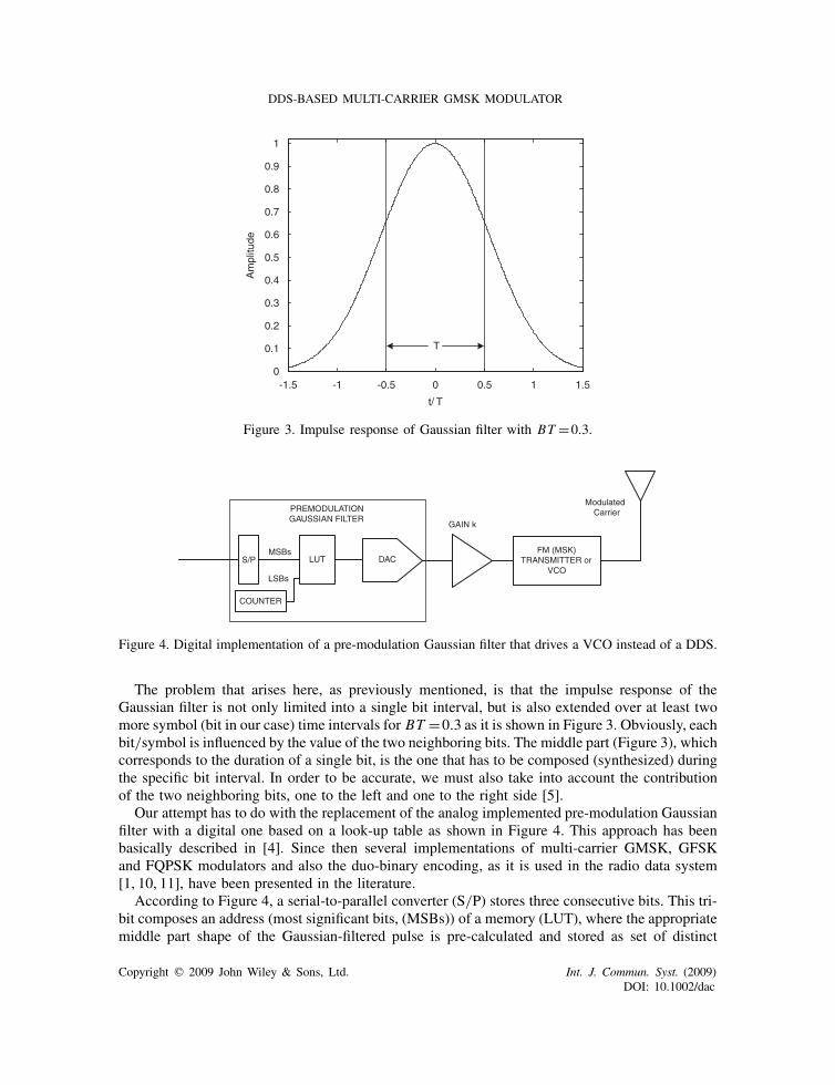
Figure 3. Impulse response of Gaussian filter with BT =0.3.
FM (MSK) TRANSMITTER or
VCO
GAIN k
Modulated CarrierPREMODULATION
GAUSSIAN FILTER
LUTS/PMSBs
COUNTER
LSBs
DAC
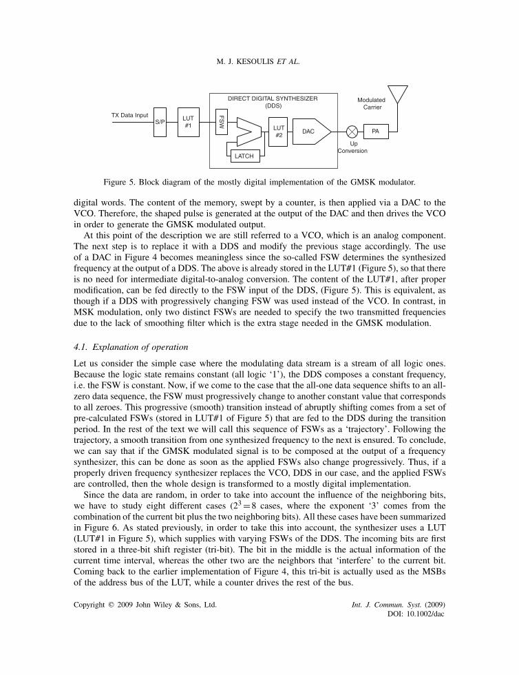
Figure 4. Digital implementation of a pre-modulation Gaussian filter that drives a VCO instead of a DDS.
The problem that arises here, as previously mentioned, is that the impulse response of theGaussian filter is not only limited into a single bit interval, but is also extended over at least twomore symbol (bit in our case) time intervals for BT =0.3 as it is shown in Figure 3. Obviously, eachbit/symbol is influenced by the value of the two neighboring bits. The middle part (Figure 3), whichcorresponds to the duration of a single bit, is the one that has to be composed (synthesized) duringthe specific bit interval. In order to be accurate, we must also take into account the contributionof the two neighboring bits, one to the left and one to the right side [5].
Our attempt has to do with the replacement of the analog implemented pre-modulation Gaussianfilter with a digital one based on a look-up table as shown in Figure 4. This approach has beenbasically described in [4]. Since then several implementations of multi-carrier GMSK, GFSKand FQPSK modulators and also the duo-binary encoding, as it is used in the radio data system[1, 10, 11], have been presented in the literature.
According to Figure 4, a serial-to-parallel converter (S/P) stores three consecutive bits. This tri-bit composes an address (most significant bits, (MSBs)) of a memory (LUT), where the appropriatemiddle part shape of the Gaussian-filtered pulse is pre-calculated and stored as set of distinct
Copyright q 2009 John Wiley & Sons, Ltd. Int. J. Commun. Syst. (2009)DOI: 10.1002/dac
M. J. KESOULIS ET AL.
Modulated Carrier
DIRECT DIGITAL SYNTHESIZER (DDS)
LUT#1 LUT
#2
FS
W
TX Data InputS/P
LATCH
PA
Up Conversion
DAC
Figure 5. Block diagram of the mostly digital implementation of the GMSK modulator.
digital words. The content of the memory, swept by a counter, is then applied via a DAC to theVCO. Therefore, the shaped pulse is generated at the output of the DAC and then drives the VCOin order to generate the GMSK modulated output.
At this point of the description we are still referred to a VCO, which is an analog component.The next step is to replace it with a DDS and modify the previous stage accordingly. The useof a DAC in Figure 4 becomes meaningless since the so-called FSW determines the synthesizedfrequency at the output of a DDS. The above is already stored in the LUT#1 (Figure 5), so that thereis no need for intermediate digital-to-analog conversion. The content of the LUT#1, after propermodification, can be fed directly to the FSW input of the DDS, (Figure 5). This is equivalent, asthough if a DDS with progressively changing FSW was used instead of the VCO. In contrast, inMSK modulation, only two distinct FSWs are needed to specify the two transmitted frequenciesdue to the lack of smoothing filter which is the extra stage needed in the GMSK modulation.
4.1. Explanation of operation
Let us consider the simple case where the modulating data stream is a stream of all logic ones.Because the logic state remains constant (all logic ‘1’), the DDS composes a constant frequency,i.e. the FSW is constant. Now, if we come to the case that the all-one data sequence shifts to an all-zero data sequence, the FSW must progressively change to another constant value that correspondsto all zeroes. This progressive (smooth) transition instead of abruptly shifting comes from a set ofpre-calculated FSWs (stored in LUT#1 of Figure 5) that are fed to the DDS during the transitionperiod. In the rest of the text we will call this sequence of FSWs as a ‘trajectory’. Following thetrajectory, a smooth transition from one synthesized frequency to the next is ensured. To conclude,we can say that if the GMSK modulated signal is to be composed at the output of a frequencysynthesizer, this can be done as soon as the applied FSWs also change progressively. Thus, if aproperly driven frequency synthesizer replaces the VCO, DDS in our case, and the applied FSWsare controlled, then the whole design is transformed to a mostly digital implementation.
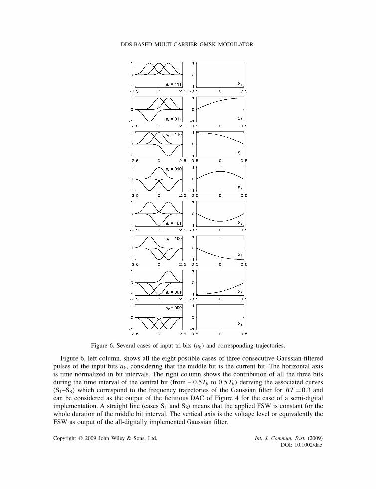
Since the data are random, in order to take into account the influence of the neighboring bits,we have to study eight different cases (23=8 cases, where the exponent ‘3’ comes from thecombination of the current bit plus the two neighboring bits). All these cases have been summarizedin Figure 6. As stated previously, in order to take this into account, the synthesizer uses a LUT(LUT#1 in Figure 5), which supplies with varying FSWs of the DDS. The incoming bits are firststored in a three-bit shift register (tri-bit). The bit in the middle is the actual information of thecurrent time interval, whereas the other two are the neighbors that ‘interfere’ to the current bit.Coming back to the earlier implementation of Figure 4, this tri-bit is actually used as the MSBsof the address bus of the LUT, while a counter drives the rest of the bus.
Copyright q 2009 John Wiley & Sons, Ltd. Int. J. Commun. Syst. (2009)DOI: 10.1002/dac
DDS-BASED MULTI-CARRIER GMSK MODULATOR
Figure 6. Several cases of input tri-bits (ak) and corresponding trajectories.
Figure 6, left column, shows all the eight possible cases of three consecutive Gaussian-filteredpulses of the input bits ak , considering that the middle bit is the current bit. The horizontal axisis time normalized in bit intervals. The right column shows the contribution of all the three bitsduring the time interval of the central bit (from – 0.5Tb to 0.5Tb) deriving the associated curves(S1–S8) which correspond to the frequency trajectories of the Gaussian filter for BT =0.3 andcan be considered as the output of the fictitious DAC of Figure 4 for the case of a semi-digitalimplementation. A straight line (cases S1 and S8) means that the applied FSW is constant for thewhole duration of the middle bit interval. The vertical axis is the voltage level or equivalently theFSW as output of the all-digitally implemented Gaussian filter.
Copyright q 2009 John Wiley & Sons, Ltd. Int. J. Commun. Syst. (2009)DOI: 10.1002/dac
M. J. KESOULIS ET AL.
g(n)
j
a(n)
3-S
tage
Shi
ft R
egis
ter
ak
ak+1
ak-1
Address Decoder
Counter MOD 2j
Modified Gaussian
Trajectories ROM
MS
Bs
LSB
s
k k
XOR2
XOR3
j
XOR1ak+1
ak
ak-1
to XOR
to ROM
Address Decoder
amod,k-1
amod ,k+1
Figure 7. Block diagram of the digital implementation of the Gaussian filter, which takes into account thesymmetries of the frequency trajectories.
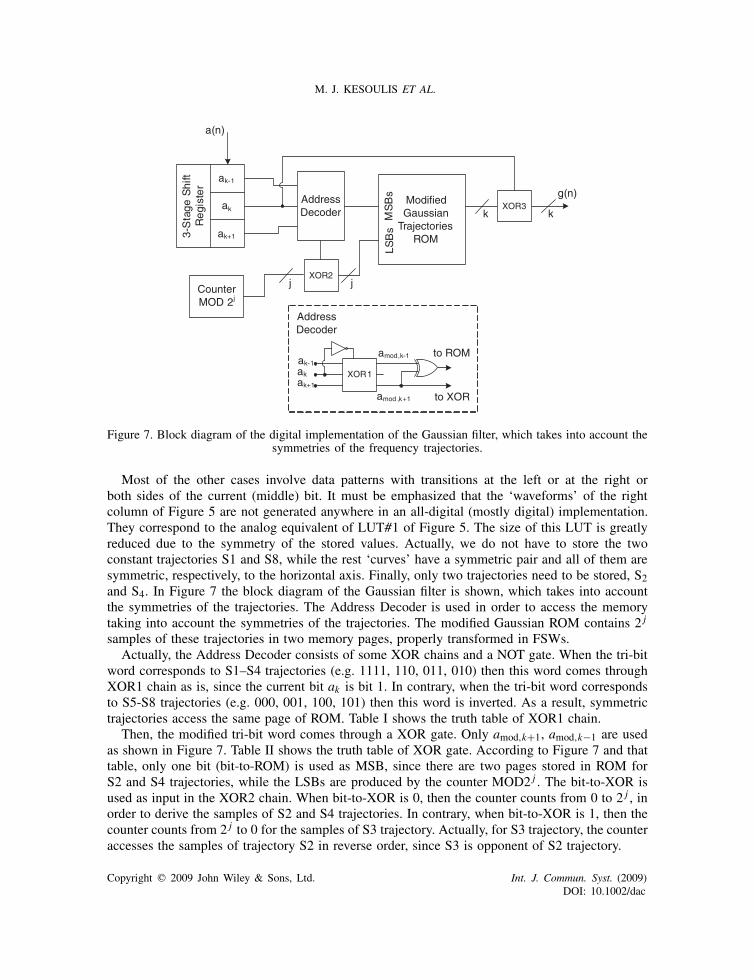
Most of the other cases involve data patterns with transitions at the left or at the right orboth sides of the current (middle) bit. It must be emphasized that the ‘waveforms’ of the rightcolumn of Figure 5 are not generated anywhere in an all-digital (mostly digital) implementation.They correspond to the analog equivalent of LUT#1 of Figure 5. The size of this LUT is greatlyreduced due to the symmetry of the stored values. Actually, we do not have to store the twoconstant trajectories S1 and S8, while the rest ‘curves’ have a symmetric pair and all of them aresymmetric, respectively, to the horizontal axis. Finally, only two trajectories need to be stored, S2and S4. In Figure 7 the block diagram of the Gaussian filter is shown, which takes into accountthe symmetries of the trajectories. The Address Decoder is used in order to access the memorytaking into account the symmetries of the trajectories. The modified Gaussian ROM contains 2 j
samples of these trajectories in two memory pages, properly transformed in FSWs.Actually, the Address Decoder consists of some XOR chains and a NOT gate. When the tri-bit
word corresponds to S1–S4 trajectories (e.g. 1111, 110, 011, 010) then this word comes throughXOR1 chain as is, since the current bit ak is bit 1. In contrary, when the tri-bit word correspondsto S5-S8 trajectories (e.g. 000, 001, 100, 101) then this word is inverted. As a result, symmetrictrajectories access the same page of ROM. Table I shows the truth table of XOR1 chain.
Then, the modified tri-bit word comes through a XOR gate. Only amod,k+1, amod,k−1 are usedas shown in Figure 7. Table II shows the truth table of XOR gate. According to Figure 7 and thattable, only one bit (bit-to-ROM) is used as MSB, since there are two pages stored in ROM forS2 and S4 trajectories, while the LSBs are produced by the counter MOD2 j . The bit-to-XOR isused as input in the XOR2 chain. When bit-to-XOR is 0, then the counter counts from 0 to 2 j , inorder to derive the samples of S2 and S4 trajectories. In contrary, when bit-to-XOR is 1, then thecounter counts from 2 j to 0 for the samples of S3 trajectory. Actually, for S3 trajectory, the counteraccesses the samples of trajectory S2 in reverse order, since S3 is opponent of S2 trajectory.
Copyright q 2009 John Wiley & Sons, Ltd. Int. J. Commun. Syst. (2009)DOI: 10.1002/dac
DDS-BASED MULTI-CARRIER GMSK MODULATOR
Table I. Truth table of XOR1 chain.
Tri-bit word ak XOR1 output
111 1 111110 1 110011 1 011010 1 010000 0 111001 0 110100 0 011101 0 010
Table II. Truth table of XOR gate.
amod,k+1 amod,k−1 bit-to-ROM bit-to-XOR
0 0 0 00 1 1 01 0 1 11 1 0 1
Address Decoder and counter access the ROM and derive S2, S3, S4 trajectories, while S1trajectory is constant and is generated differently. For S5, S6 and S7 trajectories, as shown inFigure 7, XOR3 chain is used. This chain reverses the output bits of the memory when ak is0, because, as referred, S1–S8, S2–S6, S3–S7 and S4–S5 are symmetric to horizontal axis. Thememory reduction is about 75%. If S1–S8 were stored in ROM, then the required memory wouldbe 8∗2 j ∗k, where k is the number of output bits of ROM, while in this case the required memoryis 2∗2 j ∗k.
The number of samples stored in this memory, 2 j , depends on the required accuracy of responseof the implementation, whereas the number k of the output bits of LUT#1 depends on the size ofthe phase accumulator of the DDS. This dependence is due to the characteristics of the GMSKmodulation, since the upper frequency must be f+ = fC +Rb/4 and the lower frequency must bef− = fC −Rb/4, i.e. the frequency deviation is � f = Rb/4, where Rb is the bit rate and fC is thecarrier frequency.
According to the specifications of the GSM standard, the data rate is Rb =270.833kbps. Then,the characteristics of the Gaussian filter can be calculated:
• We choose S=32 as the number of samples for each ‘waveform’ of the right column ofFigure 6, i.e. the FSW changes 32 times during one trajectory period. Since Rb =270.833kbpswe have fclk= S ·Rb=8.66MHz.
• For the length of the words stored in the memory, we must have: fout=2k fclk/2N�� f , where� f = Rb/4 is the frequency deviation, k is the number of the output bits of the LUT#1 andN =16 is the number of bits of the phase accumulator. This gives k�10.
• Computation of the maximum required FSWmax:
� f = FSWmax fclk2N
⇔FSWmax= Rb
4
2N
fclk⇔FSWmax=512 (4)
Copyright q 2009 John Wiley & Sons, Ltd. Int. J. Commun. Syst. (2009)DOI: 10.1002/dac
M. J. KESOULIS ET AL.
Table III. Frequency setting word samples.
Trajectory 011 0 30 60 90 120 149 178 205232 257 282 305 327 347 366 384401 416 429 442 453 463 472 480487 493 498 502 506 508 510 512
010 0 26 51 77 102 123 148 169184 200 215 230 241 246 251 256256 251 246 241 230 215 200 184169 148 123 102 77 51 26 0
In order to produce the maximum (minimum) output frequency, we have to add (subtract) theFSWmax to the actual frequency setting word FSWC. In our implementation we can program ordecide which is the IF carrier frequency by setting independently proper FSWC values for theseveral carriers to be synthesized and add or subtract the FSWmax, which is produced by theproposed design. For example, the two stored trajectories S2 and S4, according to the previousconsideration, are given in Table III. This table contains the decimal values of trajectories S2 andS4 for k=10.
5. SINGLE CARRIER MODULATOR—SIMULATION AND EXPERIMENTAL RESULTS
To verify the proposed technique a prototype has been designed and implemented according to theabove description of the DDS and the Gaussian filter. For the implementation the XCS104PC84,a Xilinx (SPARTAN series) FPGA was used. The clock frequency was set at 8.666MHz. Forexperimental purposes a pseudo-random bit pattern generator was incorporated in the same FPGA.In the GMSK modulator the input data are passing through a shift register. For each input bita counter sweeps the serially stored 32 samples (from 0 to 31) of the proper trajectory, whichcorrespond to the input tri-bit. The value of the trajectory sample, added/subtracted to the FSWCdrives the output of the synthesizer to the synthesized frequency in the range from the higher( fc+Rb/4) to the lower ( fc−Rb/4) output frequency.
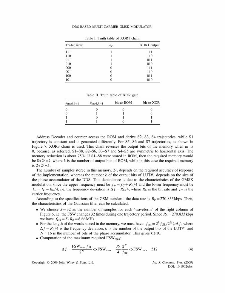
In Figure 8 the GMSK modulated signal in the IF stage is shown from both the simulation andthe oscilloscope image capture. As it is shown the simulation and experimental waveforms are verysimilar. In measurements, the carrier frequency was set equal to fc=938KHz by the appropriateFSWC. The phase continuity that gives smooth transition from the lower ( fc−Rb/4) to the upperfrequency ( fc+Rb/4) as well as the flat envelope is obvious.
In Figure 9 an image capture from the spectrum analyzer of the output of the implementedGMSK modulator is shown. The spectrum and the suppression of the side lobes are the onesexpected from theory [3]: the main lobe of the spectrum of the GMSK modulation is 1.5 timeswider than the corresponding of the QPSK modulation, i.e. the equivalent bandwidth is 1.5Rb andB99%=1.5Rb=406.25KHz, as shown in Figure 9.
6. TWO-CARRIER MODULATOR—SIMULATION AND IMPLEMENTATION
In order to demonstrate the previously proposed architecture for a multi-carrier GMSKmodulator, atwo-carrier system has been designed and implemented. The block diagram of the implementation
Copyright q 2009 John Wiley & Sons, Ltd. Int. J. Commun. Syst. (2009)DOI: 10.1002/dac
DDS-BASED MULTI-CARRIER GMSK MODULATOR
Figure 8. A single carrier modulator (simulation and oscilloscope image capture).
Figure 9. Image capture of the spectrum, (B99%=406.25KHz) of one-channel GMSK modulator.
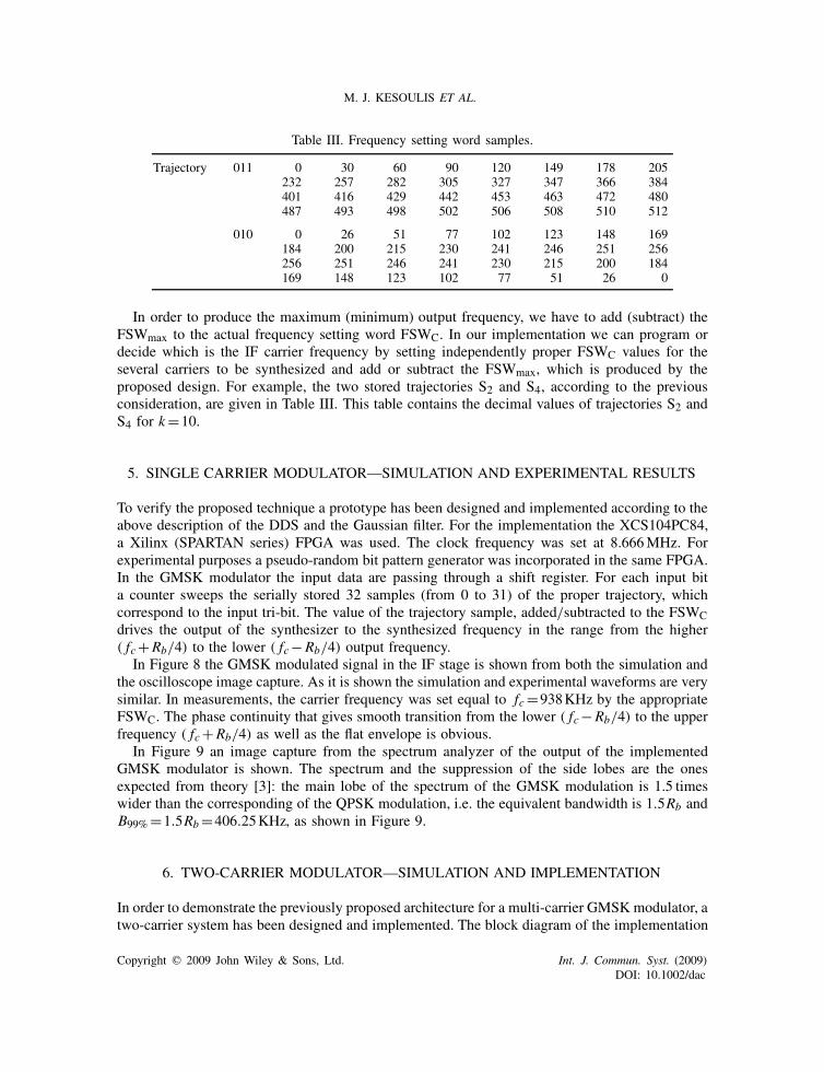
is shown in Figure 10, while the technical specifications of two-carrier GMSK modulator arepresented in Table IV. Except of the DAC and the filter, the rest of the circuit is implementedin the FPGA. As referred above, the available FPGA device was the XCS104PC84 of the XilinxSpartan series. The two-carrier implementation required 96% of the available space. We note thatdue to the re-use of most of the stages the addition of more carriers does not require proportionalspace. This is the reason why a two-carrier system was implemented instead of a multi-carrierone. In Figure 10 and all the associated figures the symbol of XOR gate denotes a single gate,whereas the box with the word XOR denotes a chain of gates, one for each line. For the requireddigital-to-analog conversion at the FPGA output, a 12-bit DAC was selected (AD-9762AR) as itis optimized both for DDS and base station applications [12]. Also it gives the opportunity to trimthe reference current by several ways that, in turn, trims the power level of the composed signal.
Copyright q 2009 John Wiley & Sons, Ltd. Int. J. Commun. Syst. (2009)DOI: 10.1002/dac
M. J. KESOULIS ET AL.
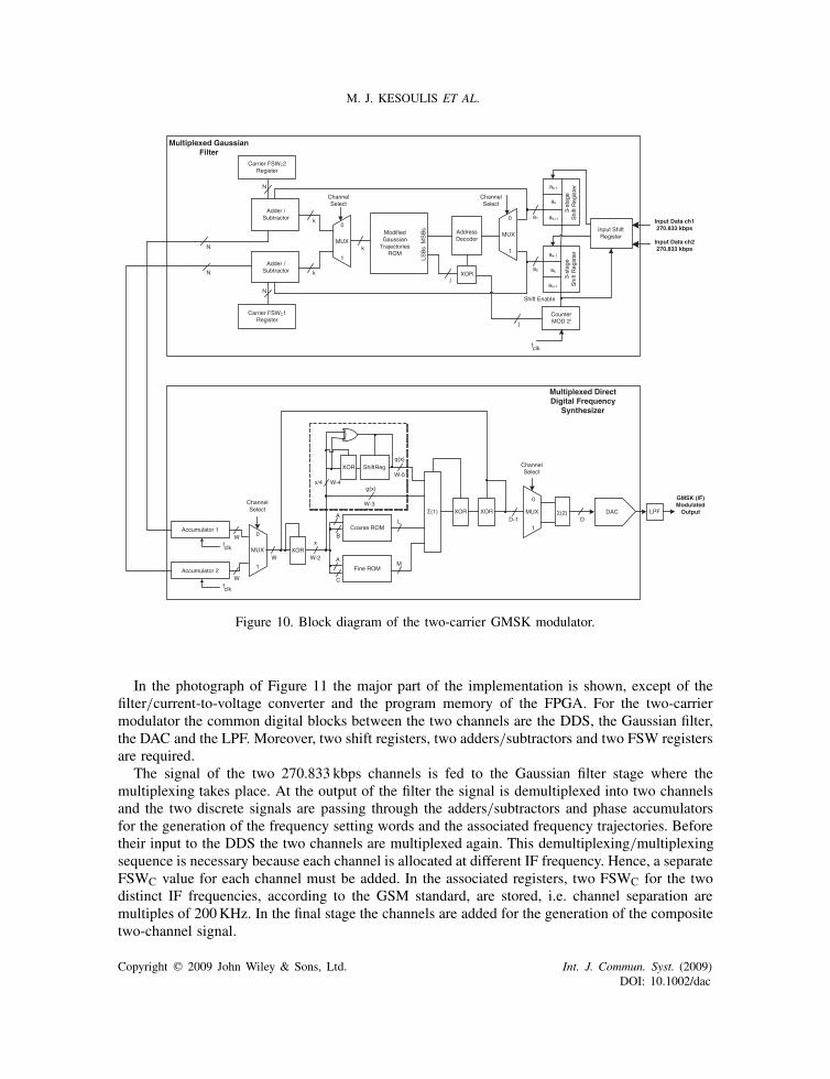
Figure 10. Block diagram of the two-carrier GMSK modulator.
In the photograph of Figure 11 the major part of the implementation is shown, except of thefilter/current-to-voltage converter and the program memory of the FPGA. For the two-carriermodulator the common digital blocks between the two channels are the DDS, the Gaussian filter,the DAC and the LPF. Moreover, two shift registers, two adders/subtractors and two FSW registersare required.
The signal of the two 270.833 kbps channels is fed to the Gaussian filter stage where themultiplexing takes place. At the output of the filter the signal is demultiplexed into two channelsand the two discrete signals are passing through the adders/subtractors and phase accumulatorsfor the generation of the frequency setting words and the associated frequency trajectories. Beforetheir input to the DDS the two channels are multiplexed again. This demultiplexing/multiplexingsequence is necessary because each channel is allocated at different IF frequency. Hence, a separateFSWC value for each channel must be added. In the associated registers, two FSWC for the twodistinct IF frequencies, according to the GSM standard, are stored, i.e. channel separation aremultiples of 200KHz. In the final stage the channels are added for the generation of the compositetwo-channel signal.
Copyright q 2009 John Wiley & Sons, Ltd. Int. J. Commun. Syst. (2009)DOI: 10.1002/dac
DDS-BASED MULTI-CARRIER GMSK MODULATOR
Table IV. Technical specifications of two-carrier GMSK modulator.
Multiplexed Gaussian filterClock frequency fclk=17.3MHzInput data rate ch1 270.833 kbpsInput data rate ch2 270.833 kbpsTotally stored modified trajectories 2 (S2, S4)Stored samples per trajectory 32 samplesInput bits of GMSK ROM j+1=6 bitsOutput bits of GMSK ROM k=10 bitsGMSK ROM size 640 bitsFSWc1 7093 (in decimal radix)Carrier frequency 1 Fc1=938kHzFSWc2 14 654 (in decimal radix)Carrier frequency 2 Fc2=1938kHz
Multiplexed direct digital synthesizerClock frequency fclk=17.3MHzAccumulator1,2 length N =16 bitsInput bits of DDS W =12 bitsOutput bits of DDS D=11 bitsFrequency resolution 132 HzSpectral purity SFDR=−61 dBcInput bits of coarse ROM A+B=6 bitsOutput bits of coarse ROM L=5 bitsInput bits of fine ROM A+C=5 bitsOutput bits of fine ROM M=4 bitsDDS ROM size (coarse and fine ROM) 448 bits
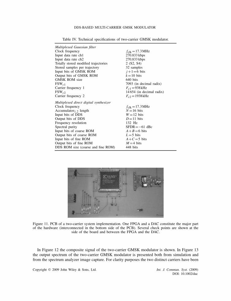
Figure 11. PCB of a two-carrier system implementation. One FPGA and a DAC constitute the major partof the hardware (interconnected in the bottom side of the PCB). Several check points are shown at the
side of the board and between the FPGA and the DAC.
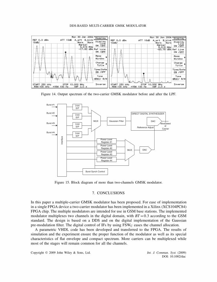
In Figure 12 the composite signal of the two-carrier GMSK modulator is shown. In Figure 13the output spectrum of the two-carrier GMSK modulator is presented both from simulation andfrom the spectrum analyzer image capture. For clarity purposes the two distinct carriers have been
Copyright q 2009 John Wiley & Sons, Ltd. Int. J. Commun. Syst. (2009)DOI: 10.1002/dac
M. J. KESOULIS ET AL.
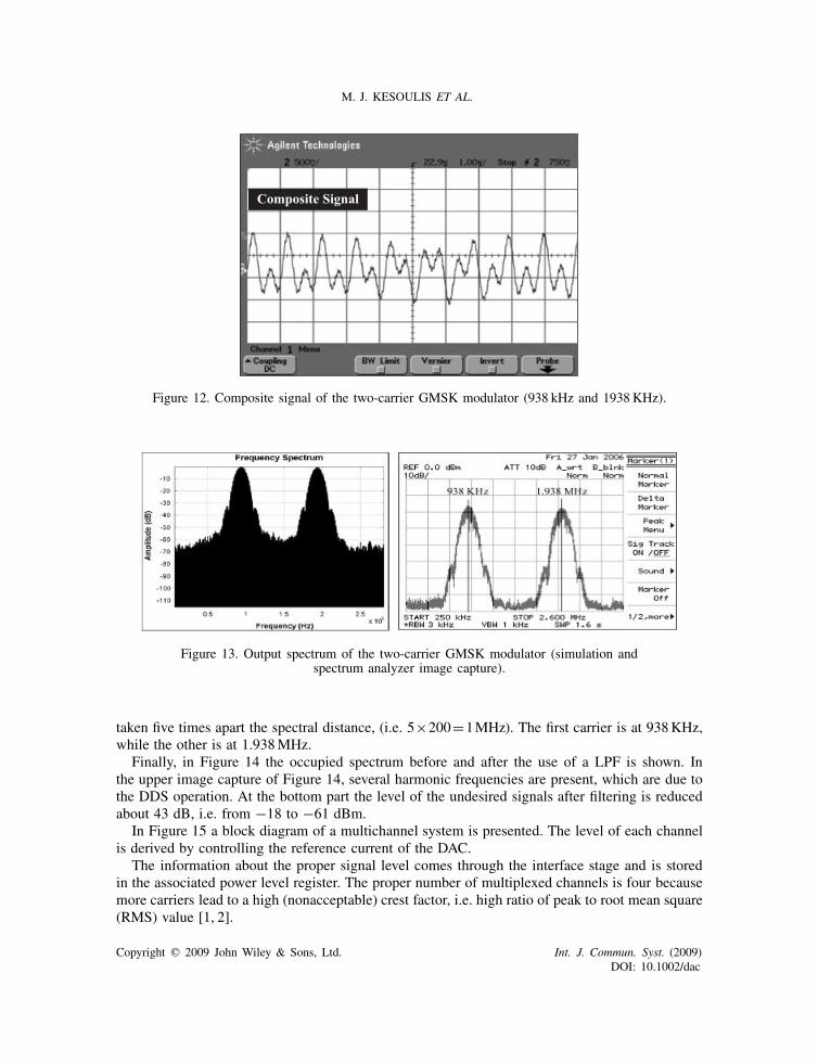
Figure 12. Composite signal of the two-carrier GMSK modulator (938 kHz and 1938 KHz).
Figure 13. Output spectrum of the two-carrier GMSK modulator (simulation andspectrum analyzer image capture).
taken five times apart the spectral distance, (i.e. 5×200=1MHz). The first carrier is at 938KHz,while the other is at 1.938MHz.
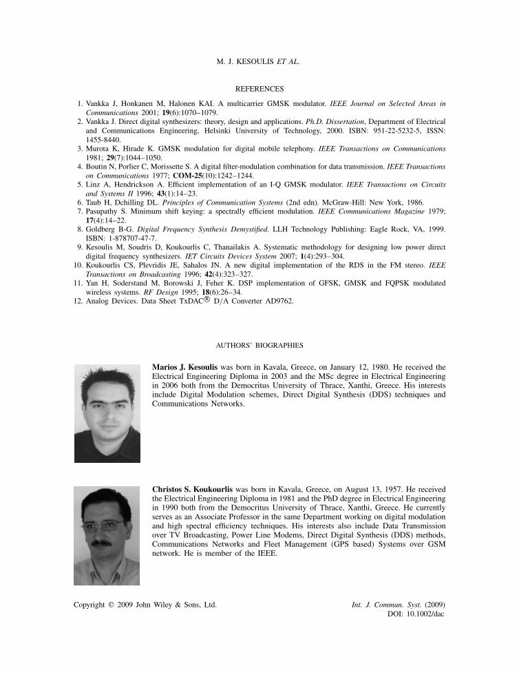
Finally, in Figure 14 the occupied spectrum before and after the use of a LPF is shown. Inthe upper image capture of Figure 14, several harmonic frequencies are present, which are due tothe DDS operation. At the bottom part the level of the undesired signals after filtering is reducedabout 43 dB, i.e. from −18 to −61 dBm.
In Figure 15 a block diagram of a multichannel system is presented. The level of each channelis derived by controlling the reference current of the DAC.
The information about the proper signal level comes through the interface stage and is storedin the associated power level register. The proper number of multiplexed channels is four becausemore carriers lead to a high (nonacceptable) crest factor, i.e. high ratio of peak to root mean square(RMS) value [1, 2].Copyright q 2009 John Wiley & Sons, Ltd. Int. J. Commun. Syst. (2009)
DOI: 10.1002/dac
DDS-BASED MULTI-CARRIER GMSK MODULATOR
Figure 14. Output spectrum of the two-carrier GMSK modulator before and after the LPF.
3-bitS/P
3-bitS/P
3-bitS/P
3-bitS/P
MUX
Inte
rfac
e
Gaussian Filter
Power Level Register #1
Power Level Register #2
Power Level Register #3
Power Level Register #4
MUX
DIRECT DIGITAL SYNTHESIZER
Burst Synch Control
Burst #1
Burst #2
Burst #3
Burst #4
ModulatedIF
CarrierReference Adjust
DAC
DAC
Figure 15. Block diagram of more than two-channels GMSK modulator.
7. CONCLUSIONS
In this paper a multiple-carrier GMSK modulator has been proposed. For ease of implementationin a single FPGA device a two-carrier modulator has been implemented in a Xilinx (XCS104PC84)FPGA chip. The multiple modulators are intended for use in GSM base stations. The implementedmodulator multiplexes two channels in the digital domain, with BT=0.3 according to the GSMstandard. The design is based on a DDS and on the digital implementation of the Gaussianpre-modulation filter. The digital control of IFs by using FSWC eases the channel allocation.
A parametric VHDL code has been developed and transferred to the FPGA. The results ofsimulation and the experiment ensure the proper function of the modulator as well as its specialcharacteristics of flat envelope and compact spectrum. More carriers can be multiplexed whilemost of the stages will remain common for all the channels.
Copyright q 2009 John Wiley & Sons, Ltd. Int. J. Commun. Syst. (2009)DOI: 10.1002/dac
M. J. KESOULIS ET AL.
REFERENCES
1. Vankka J, Honkanen M, Halonen KAI. A multicarrier GMSK modulator. IEEE Journal on Selected Areas inCommunications 2001; 19(6):1070–1079.
2. Vankka J. Direct digital synthesizers: theory, design and applications. Ph.D. Dissertation, Department of Electricaland Communications Engineering, Helsinki University of Technology, 2000. ISBN: 951-22-5232-5, ISSN:1455-8440.
3. Murota K, Hirade K. GMSK modulation for digital mobile telephony. IEEE Transactions on Communications1981; 29(7):1044–1050.
4. Boutin N, Porlier C, Morissette S. A digital filter-modulation combination for data transmission. IEEE Transactionson Communications 1977; COM-25(10):1242–1244.
5. Linz A, Hendrickson A. Efficient implementation of an I-Q GMSK modulator. IEEE Transactions on Circuitsand Systems II 1996; 43(1):14–23.
6. Taub H, Dchilling DL. Principles of Communication Systems (2nd edn). McGraw-Hill: New York, 1986.7. Pasupathy S. Minimum shift keying: a spectrally efficient modulation. IEEE Communications Magazine 1979;
17(4):14–22.8. Goldberg B-G. Digital Frequency Synthesis Demystified. LLH Technology Publishing: Eagle Rock, VA, 1999.
ISBN: 1-878707-47-7.9. Kesoulis M, Soudris D, Koukourlis C, Thanailakis A. Systematic methodology for designing low power direct
digital frequency synthesizers. IET Circuits Devices System 2007; 1(4):293–304.10. Koukourlis CS, Plevridis JE, Sahalos JN. A new digital implementation of the RDS in the FM stereo. IEEE
Transactions on Broadcasting 1996; 42(4):323–327.11. Yan H, Soderstand M, Borowski J, Feher K. DSP implementation of GFSK, GMSK and FQPSK modulated
wireless systems. RF Design 1995; 18(6):26–34.12. Analog Devices. Data Sheet TxDAC R© D/A Converter AD9762.
AUTHORS’ BIOGRAPHIES
Marios J. Kesoulis was born in Kavala, Greece, on January 12, 1980. He received theElectrical Engineering Diploma in 2003 and the MSc degree in Electrical Engineeringin 2006 both from the Democritus University of Thrace, Xanthi, Greece. His interestsinclude Digital Modulation schemes, Direct Digital Synthesis (DDS) techniques andCommunications Networks.
Christos S. Koukourlis was born in Kavala, Greece, on August 13, 1957. He receivedthe Electrical Engineering Diploma in 1981 and the PhD degree in Electrical Engineeringin 1990 both from the Democritus University of Thrace, Xanthi, Greece. He currentlyserves as an Associate Professor in the same Department working on digital modulationand high spectral efficiency techniques. His interests also include Data Transmissionover TV Broadcasting, Power Line Modems, Direct Digital Synthesis (DDS) methods,Communications Networks and Fleet Management (GPS based) Systems over GSMnetwork. He is member of the IEEE.
Copyright q 2009 John Wiley & Sons, Ltd. Int. J. Commun. Syst. (2009)DOI: 10.1002/dac
DDS-BASED MULTI-CARRIER GMSK MODULATOR
John N. Lygouras was born in Kozani, Greece in May 1955. He received the Diplomadegree and the PhD in Electrical Engineering from the Democritus University of Thrace,Greece in 1982 and 1990, respectively, both with honors. From 1982 he was a ResearchAssistant and since 2000 he is an Associate Professor at the Democritus Universityof Thrace, Department of Electrical and Computer Engineering. In 1997 he spentsix months at the University of Liverpool, Department of Electrical Engineering andElectronics as an Honorary Senior Research Fellow. His research interests are in thefield of analog and digital electronic systems design and implementation. His interestsalso include research on robotic manipulators and mobile robots trajectory planning andexecution and position control of underwater remotely operated vehicles (UROVs).
Dimitrios Soudris: Dimitrios Soudris received his Diploma in Electrical Engineeringfrom the University of Patras, Greece, in 1987. He received the PhD Degree in ElectricalEngineering, from the University of Patras in 1992. He is currently working as anAssistant Professor in the School of Electrical and Computer Engineering, Divisionof Computer Science, National Technical University of Athens, Greece. His researchinterests include low power design, parallel architectures, embedded systems designand VLSI signal processing. He has published more than 170 papers in internationaljournals and conferences. He was the leader and principal investigator in numerousresearch projects funded by the Greek Government and Industry as well as the EuropeanCommission (ESPRIT II-III-IV and 5th, 6th and 7th IST).
John N. Sahalos was born in Philippiada, Greece, in November 1943. He received hisBSc degree in Physics, in 1967 and his PhD degree in Physics, in 1974, from theUniversity of Thessaloniki, (AUTh), Thessaloniki, Greece. Except for his PhD, during1970–75, he studied in the School of Engineering of AUTh and he received his Diploma(BCE+MCE) in civil engineering, (1975). During 1972–74, he also studied in theElectronic Physics Department of AUTh and he received his professional Diploma ofpostgraduate studies in Radio-Electrology, (1975). Since 1985, he has been a Professorat the School of Science, AUTh, where he is the director of the postgraduate studiesin Electronic Physics and the director of the RadioCommunications Laboratory (RCL).During 1989, he was a visiting Professor at the Technical University of Madrid, Spain.He is the author of four books, five book chapters and more than 300 articles publishedin the scientific literature. He has supervised 21 PhDs and more than 100 postgraduate
diploma theses. His research interests are in the areas of antennas, high frequency methods, communications,applied electromagnetics, microwaves and biomedical engineering. Prof. Sahalos is an IEEE Fellow. He is alsoa Member of the Academy of Science of New York. He is a Professional Engineer and a Consultant in theindustry. He is a member of the Greek Physical Society and of the Technical Chamber of Greece. In 2002-04,he was on the Board of Directors of the OTE, the largest Telecommunications Company in Southeast Europe.
Copyright q 2009 John Wiley & Sons, Ltd. Int. J. Commun. Syst. (2009)DOI: 10.1002/dac