COURSE STRUCTURE & SYLLABUS M.Tech ECE VLSI, VLSI Design ...
Design Verification and Test of Digital VLSI Circuits NPTEL Video Course
Module-I
Lecture-I
Introduction to Digital VLSI Design Flow
Introduction
The functionality of electronics equipments and gadgets has achieved a phenomenal while their physical sizes and weights have come down drastically. The major reason is due to the rapid advances in integration technologies, which enables fabrication of millions of transistors in a single Integrated Circuit (IC) or chip. IC (used interchangeably with “chip” in this course) is a device having multiple transistors with interconnects manufactured on a single silicon substrate. Integration with a complexity of 10’s of transistors is called Small Scale Integration, with 100’s is Medium Scale Integration (MSI), with 1000’s is Large Scale Integration (LSI), with 10,000 it is Very Large Scale Integration (VLSI) Systems of systems can be implemented in a VLSI IC. However, with this rise in functionality of VLSI ICs, design problem has become huge and complex.
Introduction
• To address this complexly issue, after the design specifications are complete almost all the other steps are automated using CAD tools.
•However, even designs automated using CAD tools may have bugs.
•Also, due to extremely large size of the design space it is not possible to verify correctness of the design under all possible situations.
•So technique are required that can verify, without exercising exhaustive input-output combinations, that the design meets all the input specifications; this technique is called formal verification.
•In VLSI designs millions of transistors are packed into a single chip. This leads to manufacturing defects and all the chips need to be physically tested by giving input signals from a pattern generator and comparing responses using a logic analyzer; this process is called Testing.
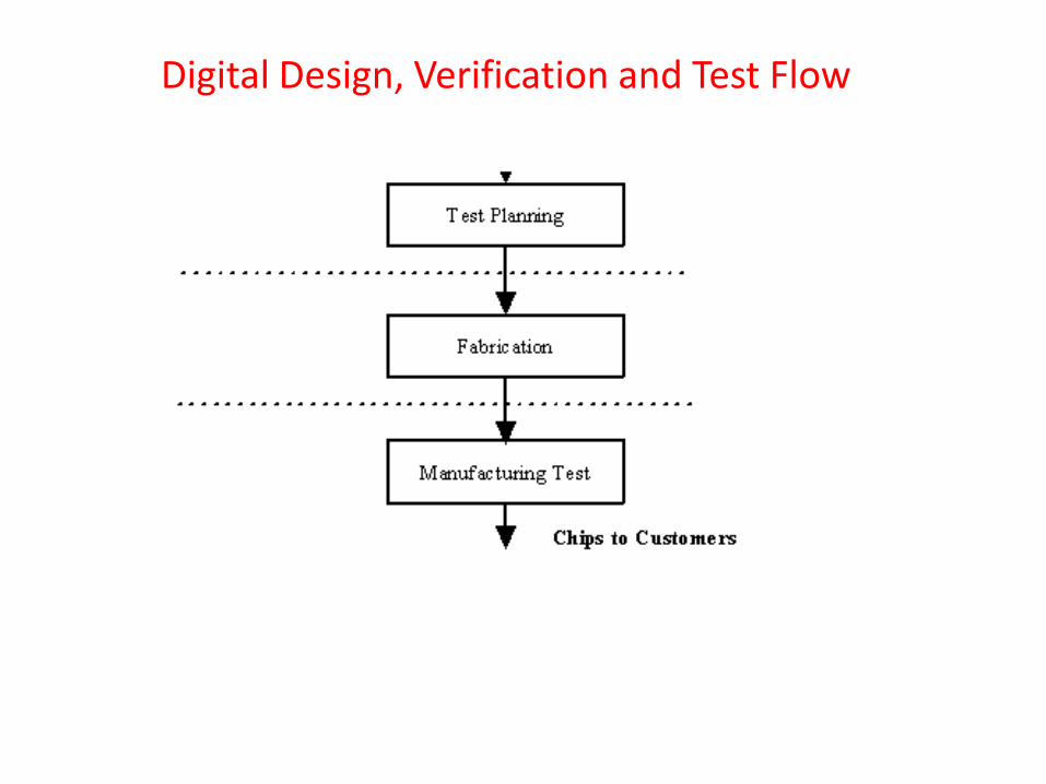
So, in the process of manufacturing a VLSI IC there are three broad steps: DESIGN-VERIFICATION-TEST.
Introduction • VLSI ICs can be divided into analog, digital or mixed-signal (both analog and digital on the same chip) based on their functionality.
•Digital ICs can contain logic gates, flip-flops, multiplexers, •Work using binary mathematics to process "one" and "zero" signals.
•Analog ICs, such as current mirrors, voltage followers, filters, OPAMPs etc. work by processing continuous signals.
•When single IC has both analog and digital components it is called mixed signal IC e.g, Analog to Digital Converter (ADC).
•The automation algorithms and CAD tools are mainly available for digital ICs because transformation of design specifications to silicon implementation can be accomplished using logical procedures (which can be converted to algorithms and tools). •However, most of the analog circuits design is like an “art” which is best performed by designers with “aid” of some CAD tools (which provides feedback to designer if the manual design is progressing fine etc.)
Introduction
• In this course we will deal only with digital VLSI circuits. Henceforth, in this course VLSI IC would imply digital VLSI ICs only and whenever we want to discuss about analog or mixed signal ICs it will be mentioned explicitly. Also, in this course the terms ICs and chips would mean VLSI ICs and chips.
• This course is concerned with algorithms required to automate the three steps “DESIGN-VERIFICATION-TEST” for Digital VLSI ICs.
Dig
ital
Des
ign
, Ver
ific
atio
n a
nd
Tes
t Fl
ow
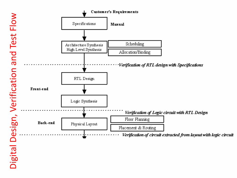
Digital Design, Verification and Test Flow
Digital Design, Verification and Test Flow
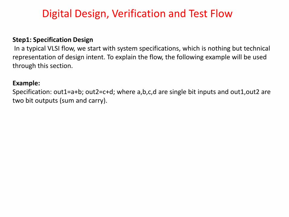
Step1: Specification Design In a typical VLSI flow, we start with system specifications, which is nothing but technical representation of design intent. To explain the flow, the following example will be used through this section. Example: Specification: out1=a+b; out2=c+d; where a,b,c,d are single bit inputs and out1,out2 are two bit outputs (sum and carry).
Digital Design, Verification and Test Flow: HLS
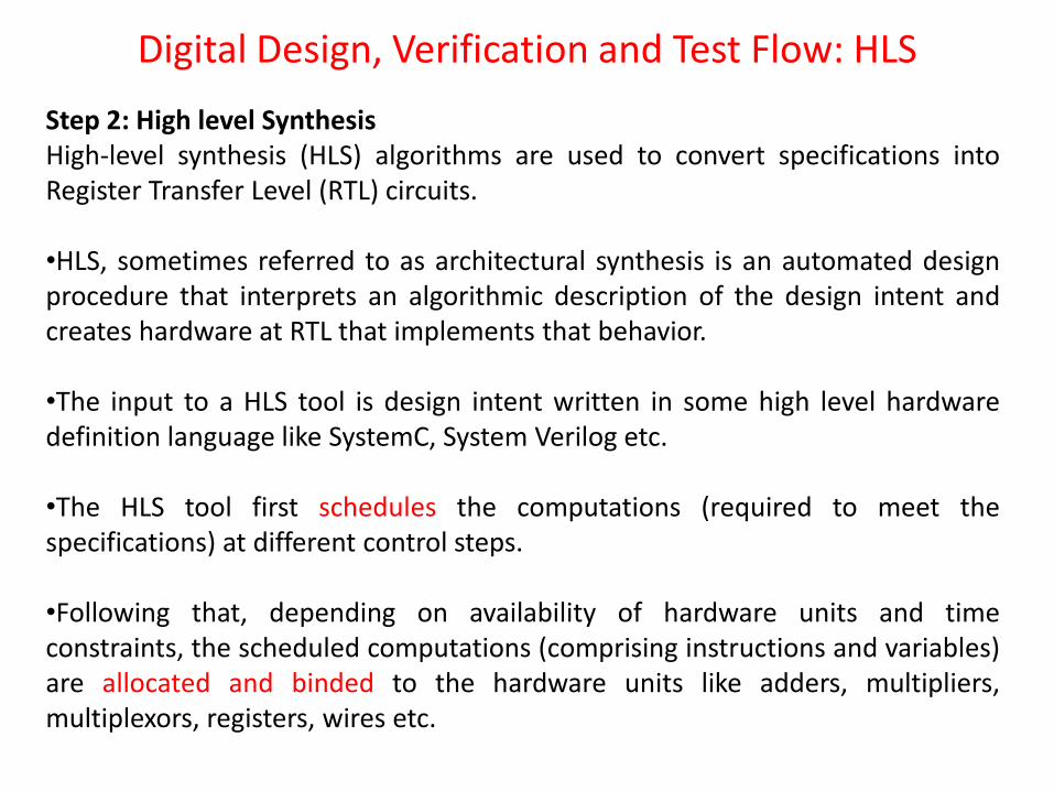
Step 2: High level Synthesis High-level synthesis (HLS) algorithms are used to convert specifications into Register Transfer Level (RTL) circuits. •HLS, sometimes referred to as architectural synthesis is an automated design procedure that interprets an algorithmic description of the design intent and creates hardware at RTL that implements that behavior.
•The input to a HLS tool is design intent written in some high level hardware definition language like SystemC, System Verilog etc.
•The HLS tool first schedules the computations (required to meet the specifications) at different control steps.
•Following that, depending on availability of hardware units and time constraints, the scheduled computations (comprising instructions and variables) are allocated and binded to the hardware units like adders, multipliers, multiplexors, registers, wires etc.
Digital Design, Verification and Test Flow: HLS
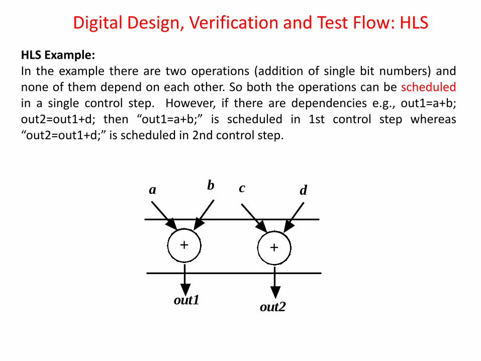
HLS Example: In the example there are two operations (addition of single bit numbers) and none of them depend on each other. So both the operations can be scheduled in a single control step. However, if there are dependencies e.g., out1=a+b; out2=out1+d; then “out1=a+b;” is scheduled in 1st control step whereas “out2=out1+d;” is scheduled in 2nd control step.
+ +
a b c d
out1out2
Digital Design, Verification and Test Flow: HLS
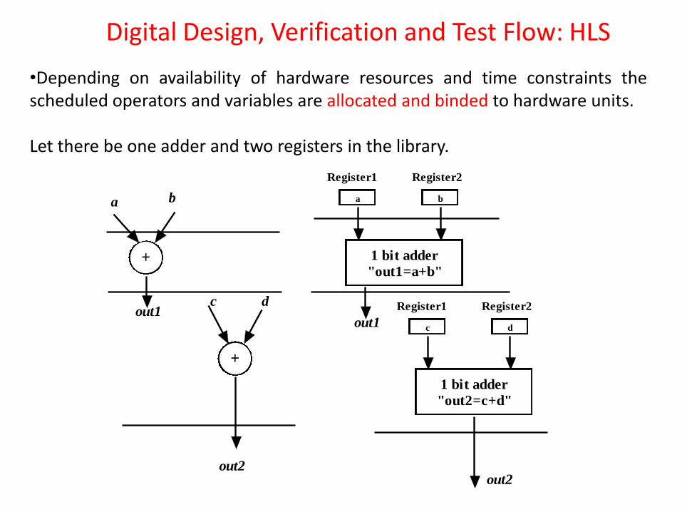
•Depending on availability of hardware resources and time constraints the scheduled operators and variables are allocated and binded to hardware units. Let there be one adder and two registers in the library.
+
+
a b
c dout1
out2
1 bit adder
"out1=a+b"
a b
Register2Register1
out1
1 bit adder
"out2=c+d"
c d
Register2Register1
out2
Digital Design, Verification and Test Flow: HLS
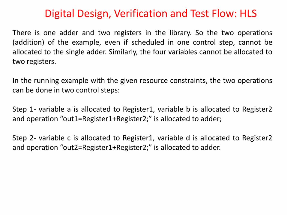
There is one adder and two registers in the library. So the two operations (addition) of the example, even if scheduled in one control step, cannot be allocated to the single adder. Similarly, the four variables cannot be allocated to two registers. In the running example with the given resource constraints, the two operations can be done in two control steps: Step 1- variable a is allocated to Register1, variable b is allocated to Register2 and operation “out1=Register1+Register2;” is allocated to adder; Step 2- variable c is allocated to Register1, variable d is allocated to Register2 and operation “out2=Register1+Register2;” is allocated to adder.
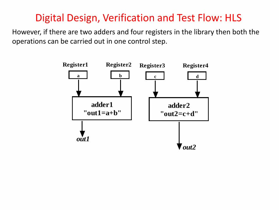
Digital Design, Verification and Test Flow: HLS However, if there are two adders and four registers in the library then both the operations can be carried out in one control step.
adder1
"out1=a+b"
a b
Register2Register1
out1
adder2
"out2=c+d"
c d
Register4Register3
out2
Digital Design, Verification and Test Flow: HLS
•Finally, based on allocation and binding, the control unit is to be designed (at high level).
•If the allocation/binding is according to (2 adders + 4 registers), the control is trivial.
•However, if the allocation is according to (1 adder + 2 registers), then the control circuit needs to provide signals that can do multiplexing between a and c, b and d;
•In 1st control step, a should be fed to Register1 and b should be fed to Register2, •In 2nd control step, c should be fed to Register1 and d should be fed to Register2.
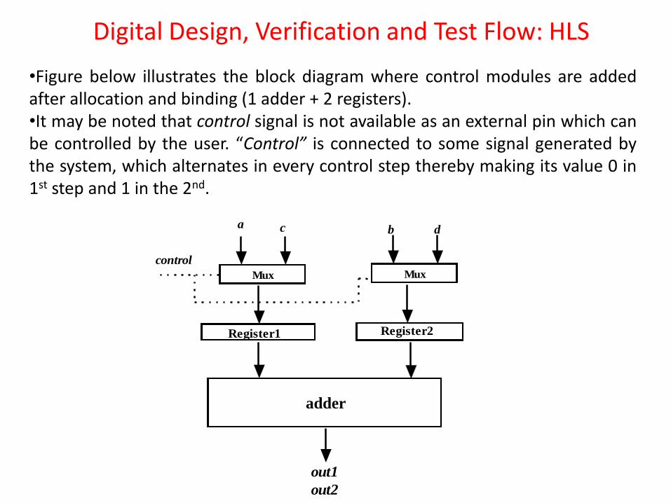
Digital Design, Verification and Test Flow: HLS
•Figure below illustrates the block diagram where control modules are added after allocation and binding (1 adder + 2 registers). •It may be noted that control signal is not available as an external pin which can be controlled by the user. “Control” is connected to some signal generated by the system, which alternates in every control step thereby making its value 0 in 1st step and 1 in the 2nd.
adder
Register2 Register1
out1
out2
Mux Mux
a c b d
control

Digital Design, Verification and Test Flow: HLS
The HLS tool generates output comprising, (i) operations-variables allocated-binded to hardware units and (ii) control modules. The output of HLS tool is called Register Transfer Level (RTL) circuit because data flow, data operations and control flow are captured between registers. After HLS, RTL circuits are transformed into logic gate level implementation; the step is called logic synthesis.
Digital Design, Verification and Test Flow: Verification
Before the staring of logic synthesis, one needs to verify if the RTL is equivalent to the specifications. In the running example, we can verify by applying all possible input conditions of a,b,c,d (along with control) to the RTL and checking if out1 and out2 are as expected. However, if the RTL has about hundreds of inputs then exercising all possible inputs is impossible because of the exponential complexity (i.e., if there are n inputs then all possible input combinations are 2n). So we need to have formal verification methods which verify equivalence of RTL with input specifications.
Broadly speaking, for formal verification we need to model the RTL circuit and the specifications using some formal modeling techniques and verify that both of them are equivalent. In other words, equivalence is determined without applying inputs. Control and Data Flow Diagram (CDFG), a formal modeling, to capture the RTL. Finite State Machine (FSM) to model the control logic. This example being very simple, we can see that both specifications and the model are equivalent. Formal techniques for checking equivalence can be will be elaborated in “VERIFICATION” section of the course.
Digital Design, Verification and Test Flow: Verification
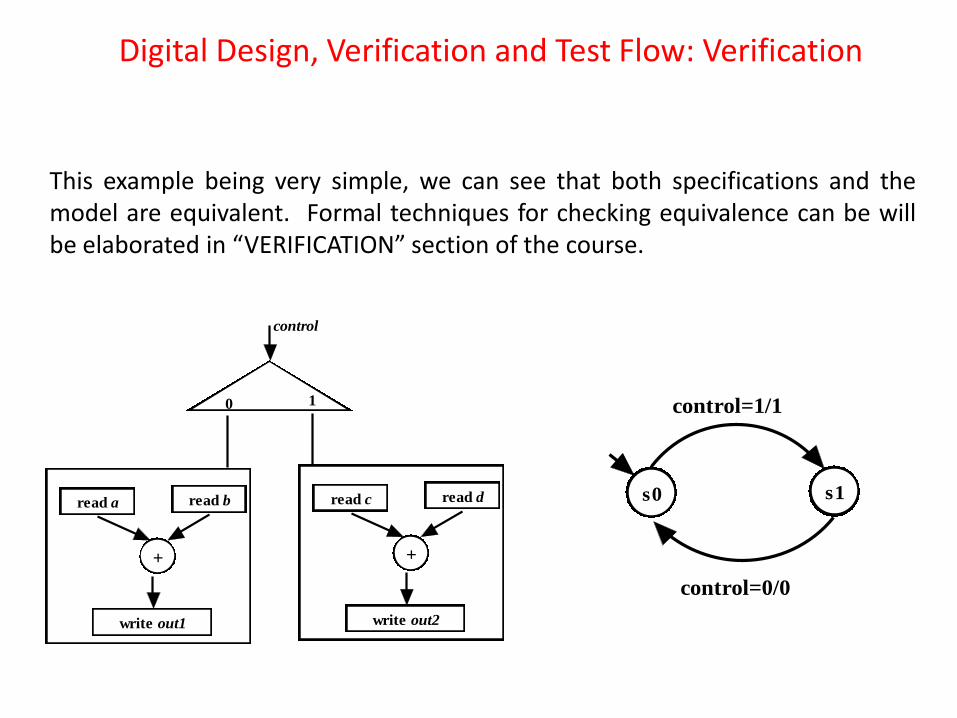
This example being very simple, we can see that both specifications and the model are equivalent. Formal techniques for checking equivalence can be will be elaborated in “VERIFICATION” section of the course.
control
0 1
read bread a
+
write out1
read dread c
+
write out2
s0 s1
control=1/1
control=0/0
Digital Design, Verification and Test Flow: Verification
Digital Design, Verification and Test Flow: Logic Synthesis
•After the RTL is verified to be equivalent to system specification, logic synthesis is performed by CAD tools. •In logic synthesis all blocks of the RTL circuit is transformed into logic gates and flip-flops.
•For the running example all the blocks namely, adder, multiplexers, control logic etc. need to be synthesized to logic gates.
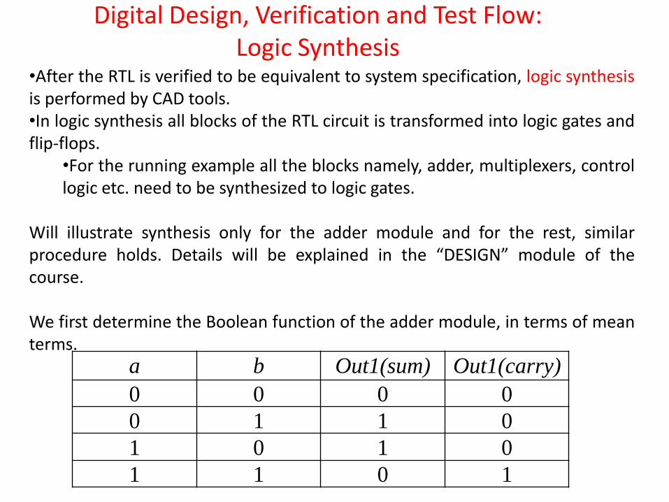
Will illustrate synthesis only for the adder module and for the rest, similar procedure holds. Details will be explained in the “DESIGN” module of the course. We first determine the Boolean function of the adder module, in terms of mean terms.
a b Out1(sum) Out1(carry)
0 0 0 0
0 1 1 0
1 0 1 0
1 1 0 1
Digital Design, Verification and Test Flow: Logic Synthesis
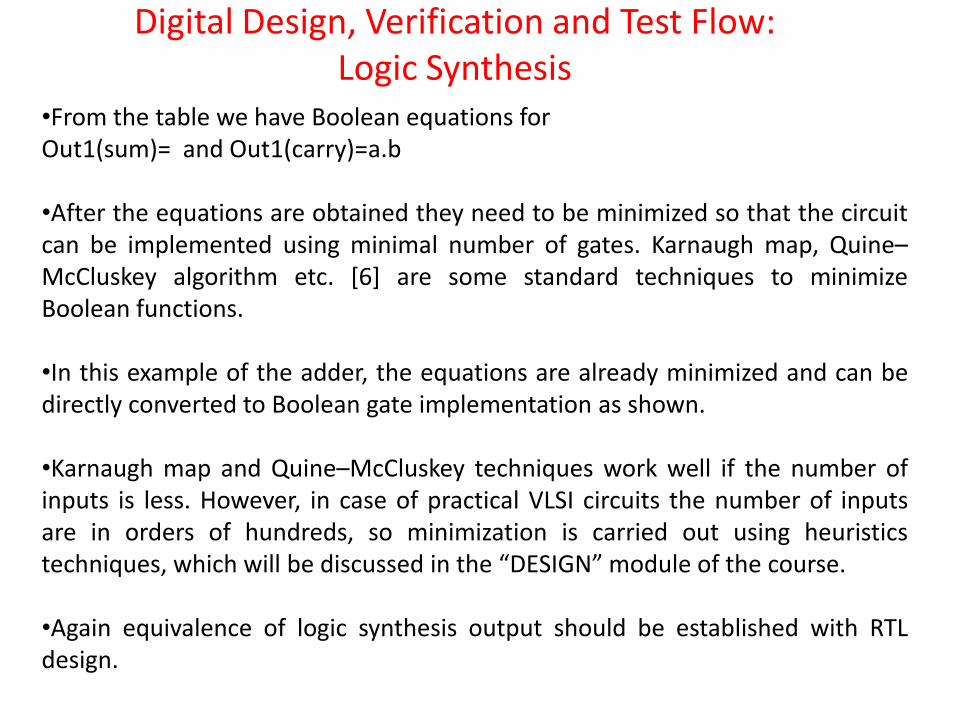
•From the table we have Boolean equations for Out1(sum)= and Out1(carry)=a.b •After the equations are obtained they need to be minimized so that the circuit can be implemented using minimal number of gates. Karnaugh map, Quine–McCluskey algorithm etc. [6] are some standard techniques to minimize Boolean functions.
•In this example of the adder, the equations are already minimized and can be directly converted to Boolean gate implementation as shown.
•Karnaugh map and Quine–McCluskey techniques work well if the number of inputs is less. However, in case of practical VLSI circuits the number of inputs are in orders of hundreds, so minimization is carried out using heuristics techniques, which will be discussed in the “DESIGN” module of the course.
•Again equivalence of logic synthesis output should be established with RTL design.
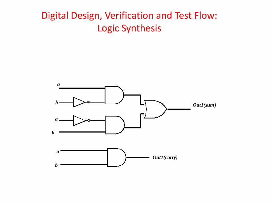
a
a
b
b
Out1(sum)
a
b
Out1(carry)
Digital Design, Verification and Test Flow: Logic Synthesis
Digital Design, Verification and Test Flow: Backend
•Once the logic level output of the circuit is obtained we move to backend phase of the design process. In backend we start with a software version of the silicon die where the chip will be finally fabricated.
•Broad plan regarding placement of gates, flip-flops etc. (output of logic synthesis) in appropriate places in the software representation of the chip; this process is called Floorplan.
•Exact locations in the die (software representation) where the circuit components are placed; this is called Placement.
•Required interconnections (as given in the logic circuit) among the gates that are placed in exact positions in the die; this process is called routing.
Again equivalence of output of Backend process should be established with logic design.
Digital Design, Verification and Test Flow: Test
•In VLSI designs millions of transistors are packed into a single chip, thereby leading to manufacturing defects. So all chips need to be physically tested by providing input signals from a pattern generator and comparing responses using a logic analyzer. • As in the case of verification, testing by applying all possible input combinations is prohibitive, due to curse of dimensionality problem. •The testing problem is more time hungry than verification because all chips need to be tested while only “one” design is to be verified. •Testing by applying all possible input combinations is called exhaustive functional testing, which is avoided because of prohibitive time requirements.
Digital Design, Verification and Test Flow: Test
•Testing is therefore done based on “structure” of the circuit and is called structural testing.
•In structural testing we first decide on set of faults that can occur, called Fault Models; stuck-at, bridging etc. are some well known fault models.
•Then we apply only those inputs which are required to validate that faults (as per fault model) are not present.
•Number of patterns required to perform structural testing is exponentially lower than that required for exhaustive functional testing.
• In Test Planning step, given a logic level circuit and fault model, we generate patterns, which when applied to a circuit determines that no fault from the fault model exists in the circuit.
Digital Design, Verification and Test Flow: Test
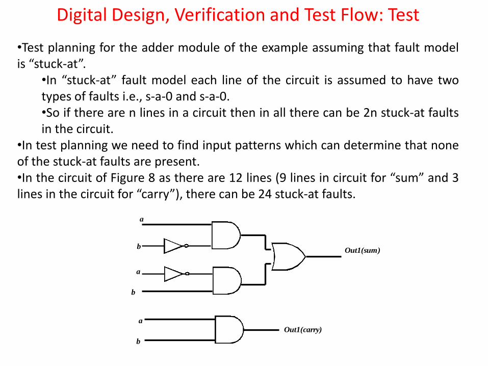
•Test planning for the adder module of the example assuming that fault model is “stuck-at”.
•In “stuck-at” fault model each line of the circuit is assumed to have two types of faults i.e., s-a-0 and s-a-0. •So if there are n lines in a circuit then in all there can be 2n stuck-at faults in the circuit.
•In test planning we need to find input patterns which can determine that none of the stuck-at faults are present. •In the circuit of Figure 8 as there are 12 lines (9 lines in circuit for “sum” and 3 lines in the circuit for “carry”), there can be 24 stuck-at faults.
a
a
b
b
Out1(sum)
a
b
Out1(carry)
Digital Design, Verification and Test Flow: Test
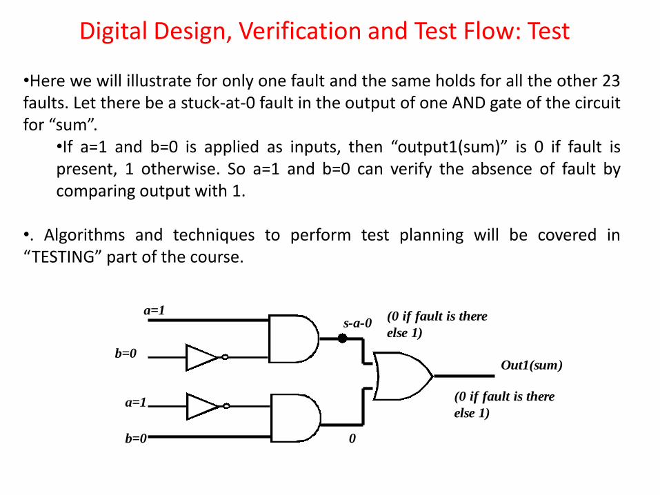
•Here we will illustrate for only one fault and the same holds for all the other 23 faults. Let there be a stuck-at-0 fault in the output of one AND gate of the circuit for “sum”.
•If a=1 and b=0 is applied as inputs, then “output1(sum)” is 0 if fault is present, 1 otherwise. So a=1 and b=0 can verify the absence of fault by comparing output with 1.
•. Algorithms and techniques to perform test planning will be covered in “TESTING” part of the course.
a=1
a=1
b=0
b=0
Out1(sum)
s-a-0
0
(0 if fault is there
else 1)
(0 if fault is there
else 1)
Digital Design, Verification and Test Flow: Fabrication, Test and Marketing
Once all steps are completed and verification after each level of transformations are done, the chips are fabricated, physically tested and fault free chips are sent for marketing.
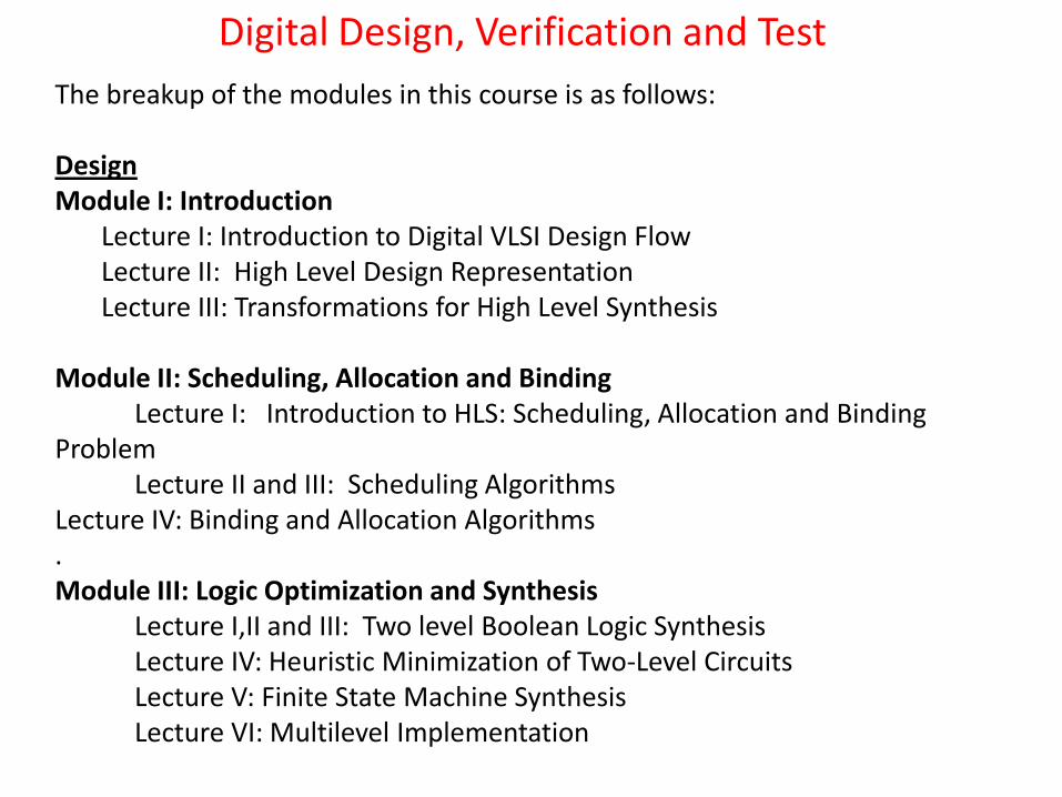
Digital Design, Verification and Test
The breakup of the modules in this course is as follows: Design Module I: Introduction Lecture I: Introduction to Digital VLSI Design Flow Lecture II: High Level Design Representation Lecture III: Transformations for High Level Synthesis Module II: Scheduling, Allocation and Binding Lecture I: Introduction to HLS: Scheduling, Allocation and Binding Problem Lecture II and III: Scheduling Algorithms Lecture IV: Binding and Allocation Algorithms . Module III: Logic Optimization and Synthesis Lecture I,II and III: Two level Boolean Logic Synthesis Lecture IV: Heuristic Minimization of Two-Level Circuits Lecture V: Finite State Machine Synthesis Lecture VI: Multilevel Implementation
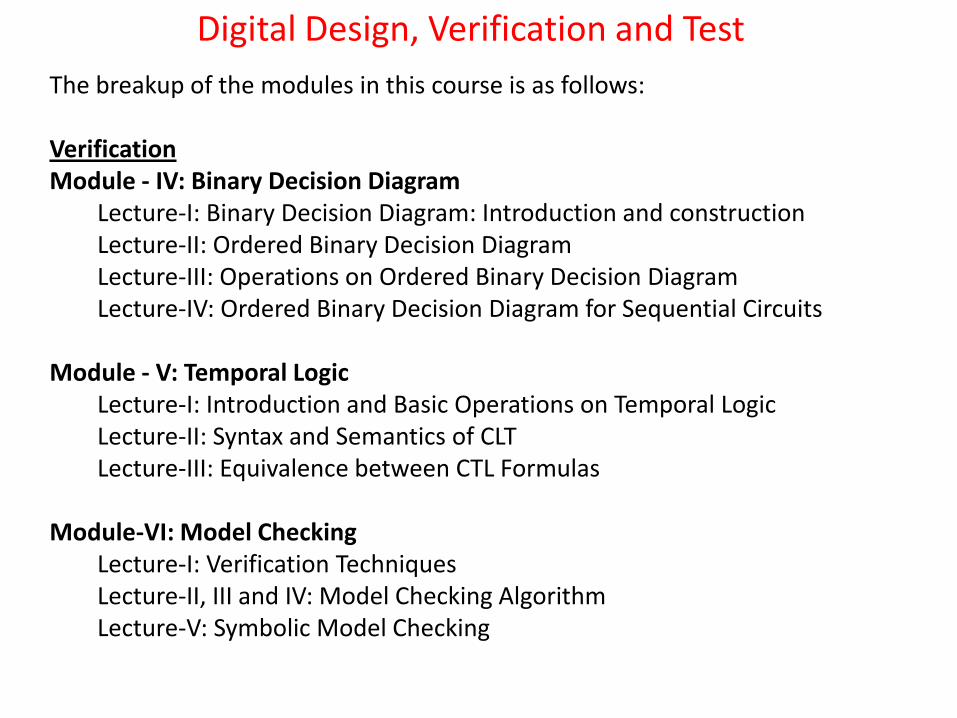
Digital Design, Verification and Test
The breakup of the modules in this course is as follows: Verification Module - IV: Binary Decision Diagram Lecture-I: Binary Decision Diagram: Introduction and construction Lecture-II: Ordered Binary Decision Diagram Lecture-III: Operations on Ordered Binary Decision Diagram Lecture-IV: Ordered Binary Decision Diagram for Sequential Circuits Module - V: Temporal Logic Lecture-I: Introduction and Basic Operations on Temporal Logic Lecture-II: Syntax and Semantics of CLT Lecture-III: Equivalence between CTL Formulas Module-VI: Model Checking Lecture-I: Verification Techniques Lecture-II, III and IV: Model Checking Algorithm Lecture-V: Symbolic Model Checking
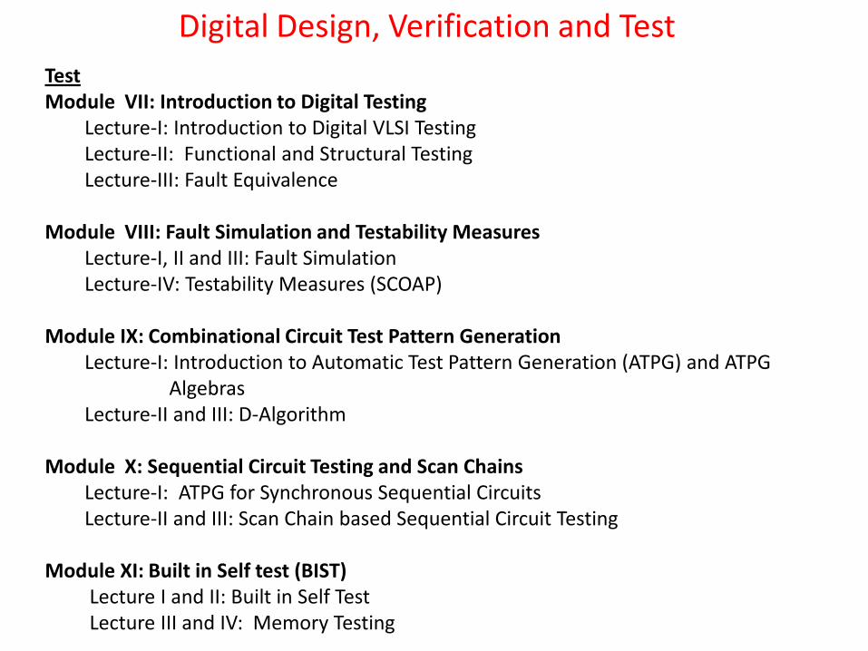
Digital Design, Verification and Test
Test Module VII: Introduction to Digital Testing Lecture-I: Introduction to Digital VLSI Testing Lecture-II: Functional and Structural Testing Lecture-III: Fault Equivalence Module VIII: Fault Simulation and Testability Measures Lecture-I, II and III: Fault Simulation Lecture-IV: Testability Measures (SCOAP) Module IX: Combinational Circuit Test Pattern Generation Lecture-I: Introduction to Automatic Test Pattern Generation (ATPG) and ATPG Algebras Lecture-II and III: D-Algorithm Module X: Sequential Circuit Testing and Scan Chains Lecture-I: ATPG for Synchronous Sequential Circuits Lecture-II and III: Scan Chain based Sequential Circuit Testing
Module XI: Built in Self test (BIST) Lecture I and II: Built in Self Test Lecture III and IV: Memory Testing
Design Verification and Test of Digital VLSI Circuits NPTEL Video Course
Module-I
Lecture-II
High Level Design Representation
Introduction
•Almost all steps of VLSI design are automated.
•Any automated procedure requires that input data being provided is in some predefined format. Also, the models used to represent the inputs and transformations (changes of the input) should be efficient for execution of the procedure.
•For example, in case of HLS the input specifications are generally in some Hardware Definition Language (HDSs) like Verilog, VHDL, System C etc.
•The HDL specifications are represented using several modeling paradigms like Control and Data Flow Diagram (CDFG) , DeJong’s hybrid flow graph, SSIM flow graph, Finite state machine with data etc., which are suitable for scheduling, allocation and binding procedures. •Sometimes timing constrains (on execution of steps) are also given in the specifications, which are modeled by the above paradigms, however, with timing parameter included e.g., CDFG with timing, DF with timing and CF with timing.
Introduction
•In this lecture, we will discuss CDFG paradigm for modeling of high-level hardware descriptions (given in Verilog). •CDFG is one of the most widely used modeling paradigm and the others mentioned above are not much different; for details of other paradigms the reader may look into the respective references.
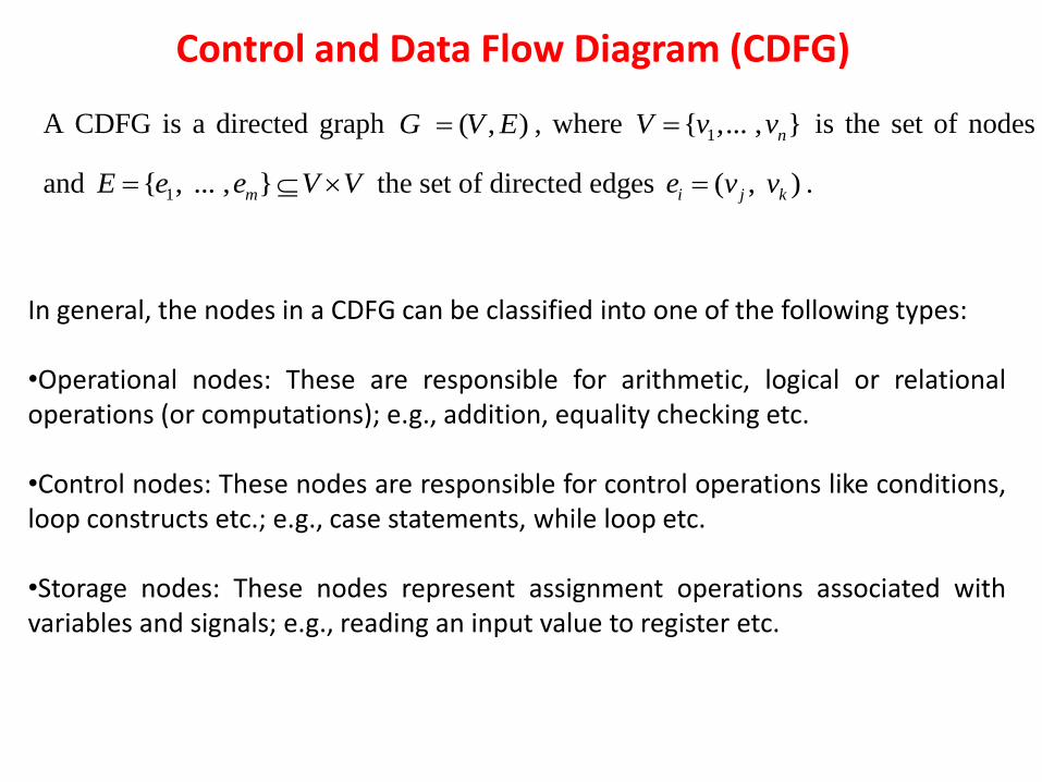
Control and Data Flow Diagram (CDFG)
In general, the nodes in a CDFG can be classified into one of the following types: •Operational nodes: These are responsible for arithmetic, logical or relational operations (or computations); e.g., addition, equality checking etc.
•Control nodes: These nodes are responsible for control operations like conditions, loop constructs etc.; e.g., case statements, while loop etc. •Storage nodes: These nodes represent assignment operations associated with variables and signals; e.g., reading an input value to register etc.
A CDFG is a directed graph ( , )G V E , where 1{ ,... , }nV v v is the set of nodes
and 1{ , ... , }mE e e V V the set of directed edges ( , )i j ke v v .
Control and Data Flow Diagram (CDFG)
The edges in a CDFG represent: •Transfer of values (in variables that are changed due to processing in operational and storage nodes). A node needs data generated by its predecessor nodes and generates new data needed by its successors. Nodes operate on the data of the incoming edges. The resulting data is put on the outgoing edges.
•Control flow from one node to another. An edge can also represent a condition, e.g., while implementing loop constructs, if/case statements etc.
Control and Data Flow Diagram (CDFG): Example
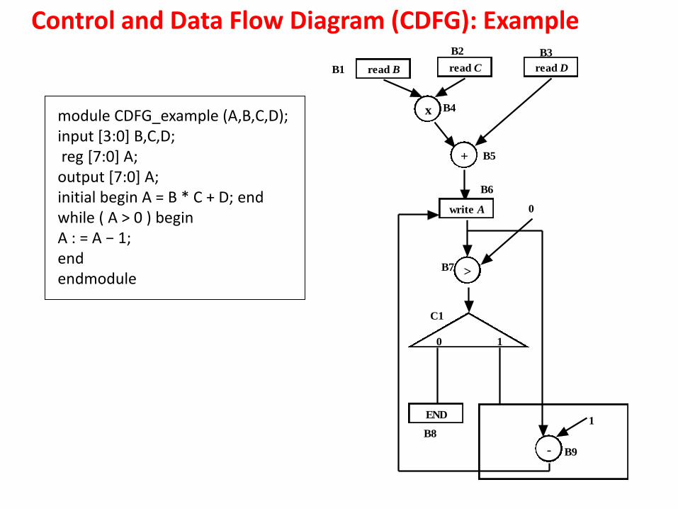
module CDFG_example (A,B,C,D); input [3:0] B,C,D; reg [7:0] A; output [7:0] A; initial begin A = B * C + D; end while ( A > 0 ) begin A : = A − 1; end endmodule
0 1
-
read Cread B
x
+
read D
write A
>
0
END1
B1
B2 B3
B4
B5
B6
B7
B8
B9
C1
Control and Data Flow Diagram (CDFG): Example
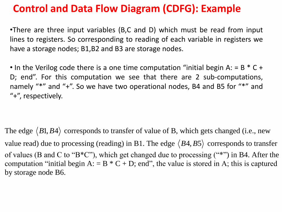
•There are three input variables (B,C and D) which must be read from input lines to registers. So corresponding to reading of each variable in registers we have a storage nodes; B1,B2 and B3 are storage nodes.
• In the Verilog code there is a one time computation “initial begin A: = B * C + D; end”. For this computation we see that there are 2 sub-computations, namely “*” and “+”. So we have two operational nodes, B4 and B5 for “*” and “+”, respectively.
The edge 1, 4B B corresponds to transfer of value of B, which gets changed (i.e., new
value read) due to processing (reading) in B1. The edge 4, 5B B corresponds to transfer
of values (B and C to “B*C”), which get changed due to processing (“*”) in B4. After the
computation “initial begin A: = B * C + D; end”, the value is stored in A; this is captured
by storage node B6.
Control and Data Flow Diagram (CDFG): Example
B7 is the operational node that checks 0 with A; output is 0 if 0A and 1,
otherwise. The output of B7 (carried by edge 7, 1B C ) controls the control node C1.
7, 1B C is the control flow edge, which corresponds to the condition (A>0) required
for execution/exit of the while loop.
Node C1 is a control node responsible for deciding data flow direction after the
condition “A>0” is checked at B7. If value transferred by 7, 1B C is 0 then the loops
exits at B8, else computation “A=A-1” is done at B9 and the loop continues.
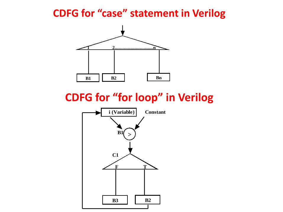
CDFG for “case” statement in Verilog
1 2.............................n
B1 B2 Bn
CDFG for “for loop” in Verilog
F T
>
B3
B1
C1
i (Variable) Constant
B2
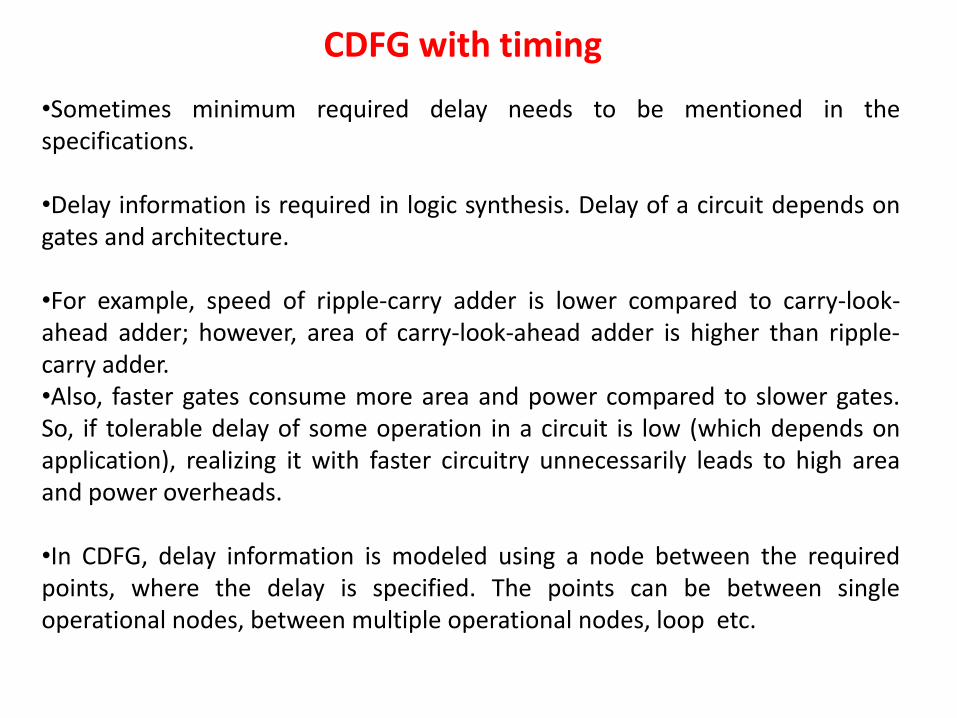
CDFG with timing
•Sometimes minimum required delay needs to be mentioned in the specifications.
•Delay information is required in logic synthesis. Delay of a circuit depends on gates and architecture.
•For example, speed of ripple-carry adder is lower compared to carry-look-ahead adder; however, area of carry-look-ahead adder is higher than ripple-carry adder. •Also, faster gates consume more area and power compared to slower gates. So, if tolerable delay of some operation in a circuit is low (which depends on application), realizing it with faster circuitry unnecessarily leads to high area and power overheads.
•In CDFG, delay information is modeled using a node between the required points, where the delay is specified. The points can be between single operational nodes, between multiple operational nodes, loop etc.
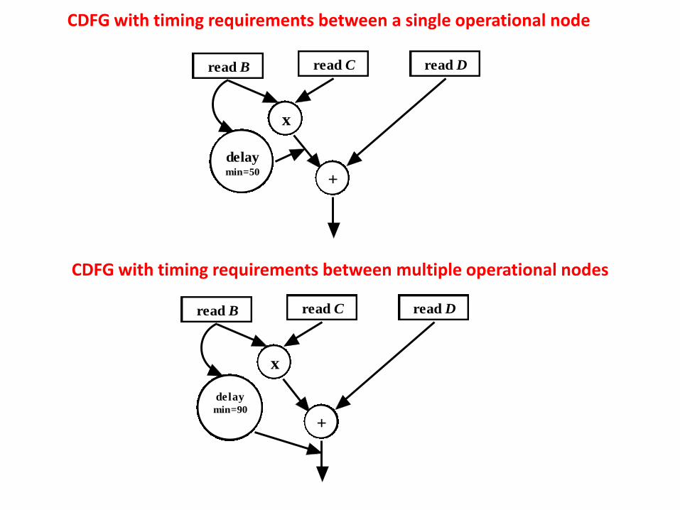
CDFG with timing requirements between a single operational node
read Cread B
x
+
read D
delaymin=50
CDFG with timing requirements between multiple operational nodes
read Cread B
x
+
read D
delaymin=90
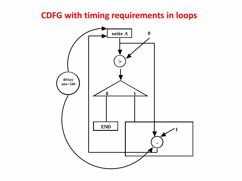
CDFG with timing requirements in loops
0 1
-
write A
>
0
END1
delaymin=100
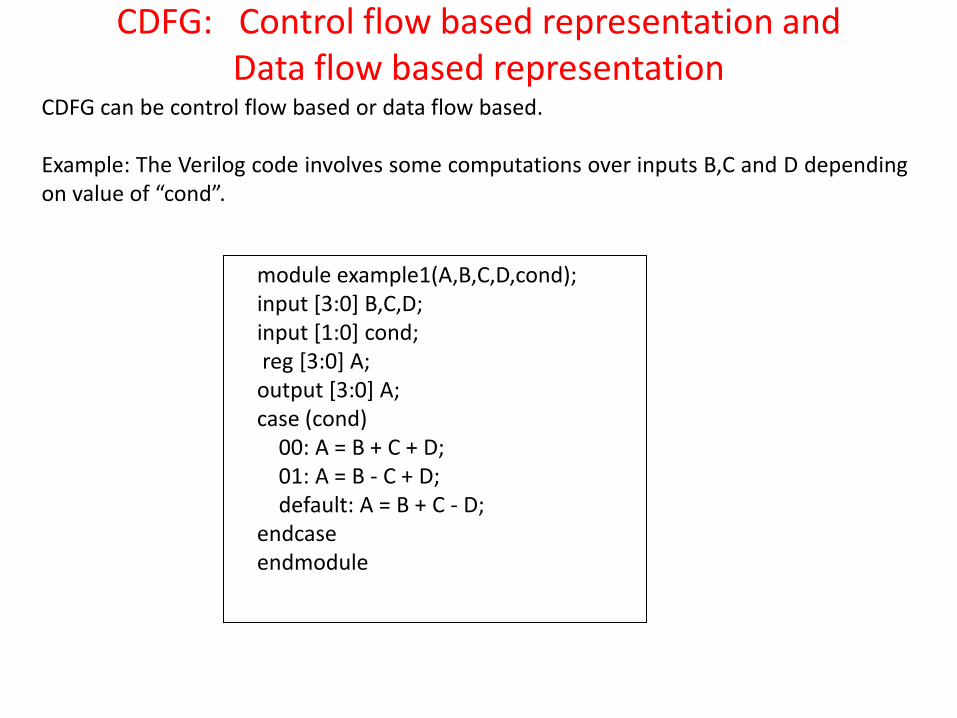
CDFG: Control flow based representation and Data flow based representation
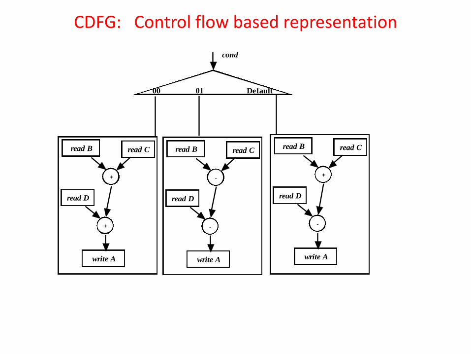
CDFG can be control flow based or data flow based. Example: The Verilog code involves some computations over inputs B,C and D depending on value of “cond”.
module example1(A,B,C,D,cond); input [3:0] B,C,D; input [1:0] cond; reg [3:0] A; output [3:0] A; case (cond) 00: A = B + C + D; 01: A = B - C + D; default: A = B + C - D; endcase endmodule
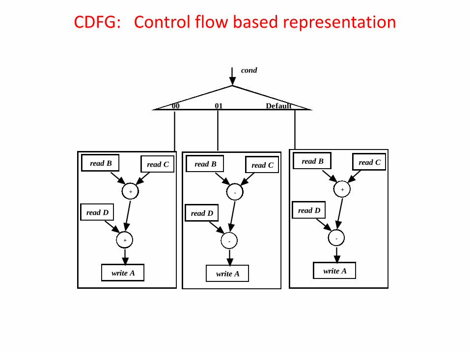
CDFG: Control flow based representation
00 01 Default
read B read C
read D
write A
+
+
read B read C
read D
write A
-
-
read B read C
read D
write A
+
-
cond
CDFG: Control flow based representation
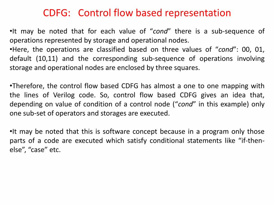
•It may be noted that for each value of “cond” there is a sub-sequence of operations represented by storage and operational nodes. •Here, the operations are classified based on three values of “cond”: 00, 01, default (10,11) and the corresponding sub-sequence of operations involving storage and operational nodes are enclosed by three squares.
•Therefore, the control flow based CDFG has almost a one to one mapping with the lines of Verilog code. So, control flow based CDFG gives an idea that, depending on value of condition of a control node (“cond” in this example) only one sub-set of operators and storages are executed.
•It may be noted that this is software concept because in a program only those parts of a code are executed which satisfy conditional statements like “if-then-else”, “case” etc.
CDFG: Control flow based representation
However, in hardware there is no concept of execution of a “sub-set” of operators/storages (i.e., statements of an HDL code), based on value of condition of a control node. In the example, variable “A” can be assigned three different values through three different computations depending on value of “cond”.
•So, three hardware circuitry are to be kept in the chip and depending on the value of “cond”, the output of appropriate circuitry would write “A”.
•In other words, unlike a software code, where parts of a code can be invoked based on values of a condition, in hardware, all the different types of circuitry are to be implemented in the chip (and would be executed) and the output being used depends on the value of a condition
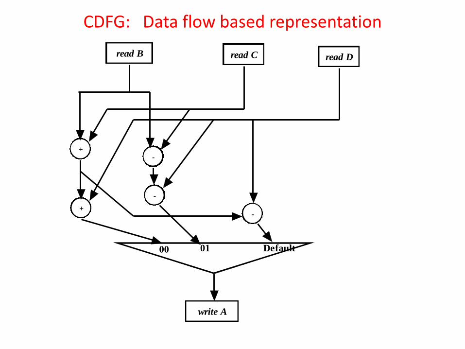
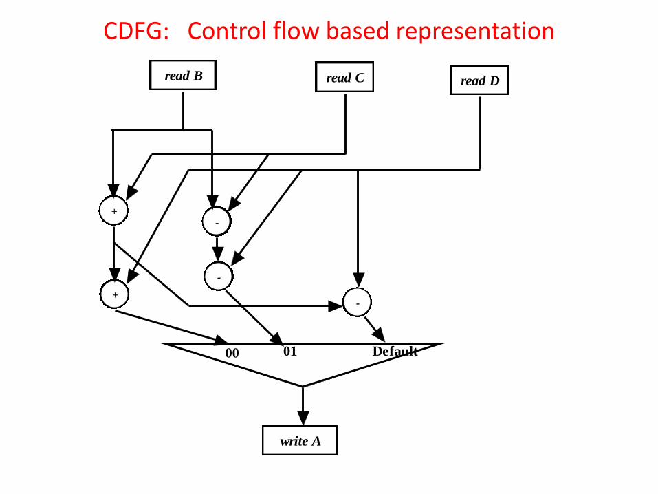
CDFG: Data flow based representation
01 Default
read B
write A
read C read D
+
+
00
-
-
-
CDFG: Data flow based representation
The control node is after the operational and storage nodes. •There are three circuits for computing different values of “A" , depending on “cond”. •The three circuits evaluate three different outputs irrespective of the value of “cond”; “A” is written by the output of the appropriate circuit depending on value of “cond”. It may also be noted that even if three different circuitry are required to compute different possible values of “A”, many operational and storage nodes are common among these circuits and redundancy can be eliminated. For example, reading of B,C,D are required by all the three circuits and they may be implemented by storage nodes common to all the three circuits. Also, operational node for “B+C” is common to circuit for “A = B + C + D” and circuit for “A = B + C - D”, which can be merged.
Question and Answer
Question: What are the advantages and disadvantages of Control flow based CDFG over Data flow based CDFG? In data flow based CDFG, we can represent parallel evaluation by operational and storage nodes for all branches of a control node. This is in real sense more near to hardware realization of the circuit, compared to that of the control flow based CDFG, where only that set of operational and storage nodes are executed for which (branch) the value of control node is satisfied. Therefore, optimizations and other steps of HLS are more suitable to be performed on data flow based CDFG. On the hand, data flow based CDFG is more tedious to draw from the specifications compared to the control flow based counterpart. In control flow based CDFG there is almost one-to-one mapping between the nodes of the CDFG and the lines of DHL code. If there are nested loops and conditions in the input specifications then it should be flattened before extracting the data flow based CDFG. Further, in such cases the CDFG may have a large number of nodes.
Design Verification and Test of Digital VLSI Circuits NPTEL Video Course
Module-I
Lecture-III
Transformations for High Level Synthesis
Introduction
•Any VLSI design starts with specifications and the first step is to obtain the Register Transfer Level (RTL) circuit.
•RTL circuit is obtained from specifications using High Level Synthesis (HLS) algorithms.
•As specifications are processed by HLS algorithms, they need to be represented using some modeling language.
•Control and Data Flow Graph (CDFG), is one of the most widely accepted modeling paradigm for specifications that are processed by HLS tools.
Introduction
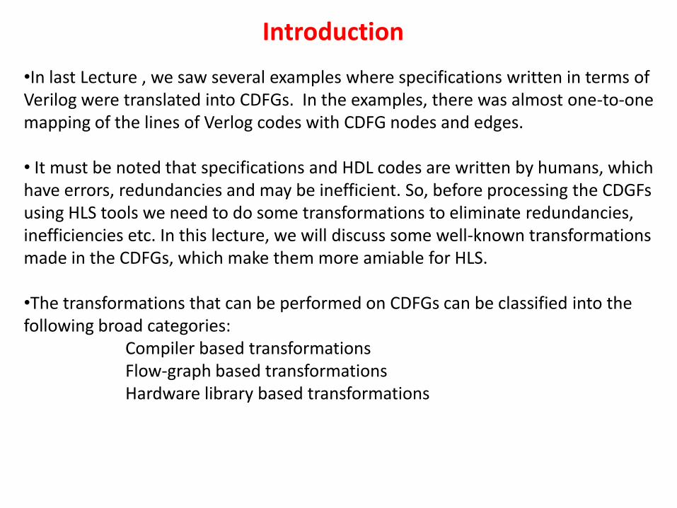
•In last Lecture , we saw several examples where specifications written in terms of Verilog were translated into CDFGs. In the examples, there was almost one-to-one mapping of the lines of Verlog codes with CDFG nodes and edges. • It must be noted that specifications and HDL codes are written by humans, which have errors, redundancies and may be inefficient. So, before processing the CDGFs using HLS tools we need to do some transformations to eliminate redundancies, inefficiencies etc. In this lecture, we will discuss some well-known transformations made in the CDFGs, which make them more amiable for HLS. •The transformations that can be performed on CDFGs can be classified into the following broad categories:
Compiler based transformations Flow-graph based transformations Hardware library based transformations
Compiler based transformations •In programming paradigm, “code optimization” is a very important step carried out by the compiler. The compiler improves the quality of a program in terms of runtime; this is called code optimization.
•Program improvement may comprise change of instruction sequence, elimination of instructions, changes in instructions itself, while retaining the meaning of the original code; these changes are called code transformations.
•Code optimization process has four components: (i) discovering opportunities to apply a transformation, (ii) proving that the transformation can be applied safely at those sites, (iii) ensuring that its application is profitable, and (iv) actually rewriting the code.
•The same philosophy can also be applied to transform a CDFG that models hardware. In case of software, code optimization reduces runtime by eliminating/reducing unnecessary computations and in case of hardware, code optimization would reduce circuit modules thereby resulting in lower area, lower power and high frequency (i.e., less computation).
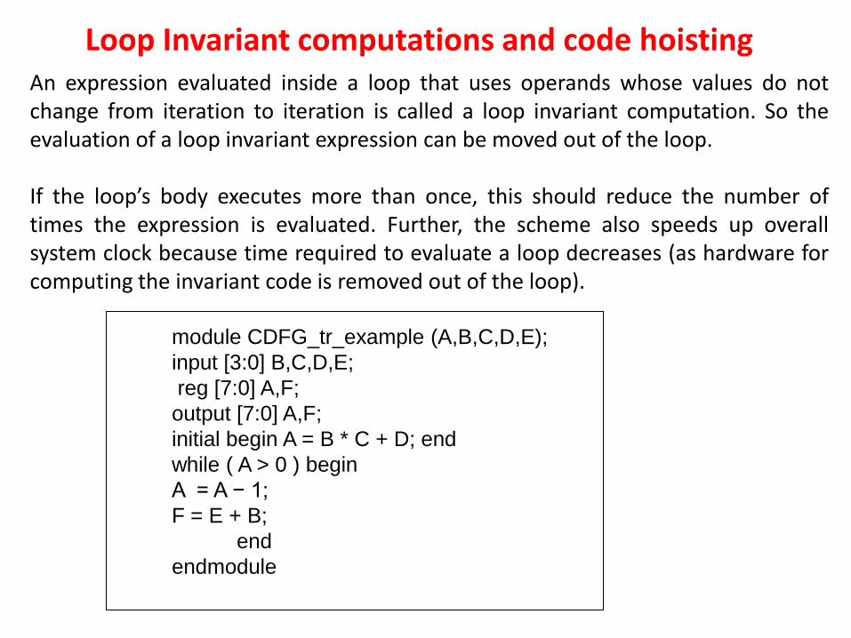
Loop Invariant computations and code hoisting An expression evaluated inside a loop that uses operands whose values do not change from iteration to iteration is called a loop invariant computation. So the evaluation of a loop invariant expression can be moved out of the loop. If the loop’s body executes more than once, this should reduce the number of times the expression is evaluated. Further, the scheme also speeds up overall system clock because time required to evaluate a loop decreases (as hardware for computing the invariant code is removed out of the loop).
module CDFG_tr_example (A,B,C,D,E);
input [3:0] B,C,D,E;
reg [7:0] A,F;
output [7:0] A,F;
initial begin A = B * C + D; end
while ( A > 0 ) begin
A = A − 1;
F = E + B;
end
endmodule
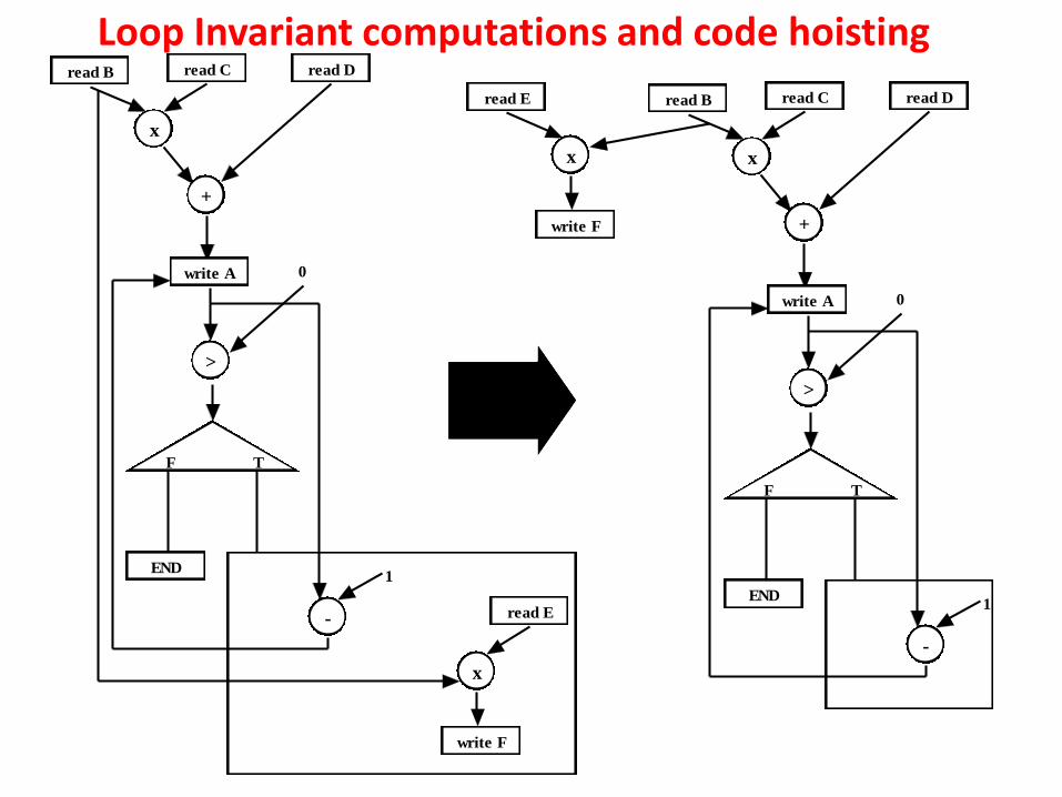
Loop Invariant computations and code hoisting
F T
-
read Cread B
x
+
read D
write A
>
0
END1
read E
x
write F
F T
-
read Cread B
x
+
read D
write A
>
0
END1
read E
x
write F
Loop Invariant computations and code hoisting
It may be noted that the computation “F = E + B;” is loop invariant, because the operands (E and B) used is the computation (to calculate F) do no change with iteration of the while loop. So we can bring the loop invariant computation “F = E + B;” before the loop begins; this is called code hosting.
Loop Invariant computations and code hoisting The conditions required to determine loop invariant computations are as follows. Any computation (or expression) can be written as “assigned variable= operand1 OPERATOR operand2… OPERATOR operandn” In terms of a CDFG, in the computation, “assigned variable” and “operand1” through “operandn” correspond to storage nodes while “OPERATOR”s corresponds to operational nodes. A computation “assigned variable=(operand1,operand2,……,operandn)” that is inside a loop, is loop invariant if 1. If all the operands are constants 2. All the computations that assign values to the operands are located outside
the loop 3. All the computations that assign values to the operands are themselves loop
invariant In the above example (Figure 1), “F = E + B;” is loop invariant because computations that assign values to the operands (F and B) are located outside the loop (taken from inputs).
Constant folding
An expression “assigned variable= operand1 OPERATOR operand2, … OPERATOR operandn” where all the operands are constants can be replaced with the pre-computed final result directly written to assigned variable. This principal of code optimization is called constant folding. Expressions, which involve computations over constants, always generate the same output irrespective of inputs. So the output of the computation over constants can be pre-computed by looking statically at the code and that output value can be directly used. So resources required for computing such expressions can be avoided.
Constant folding
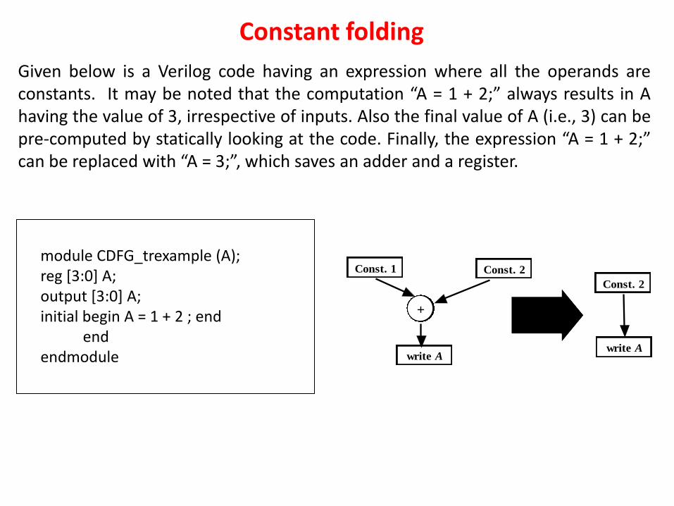
Given below is a Verilog code having an expression where all the operands are constants. It may be noted that the computation “A = 1 + 2;” always results in A having the value of 3, irrespective of inputs. Also the final value of A (i.e., 3) can be pre-computed by statically looking at the code. Finally, the expression “A = 1 + 2;” can be replaced with “A = 3;”, which saves an adder and a register.
Const. 2Const. 1
+
write Awrite A
Const. 2
module CDFG_trexample (A); reg [3:0] A; output [3:0] A; initial begin A = 1 + 2 ; end end endmodule
Redundant computation elimination
If there are two expressions “assigned variable1=operand11 OPERATOR11,..,OPERATOR1(n-1) operand1n” and “assigned variable2=operand21 OPERATOR21,..,OPERATOR2(n-1) operand2n” where, operand11=operand21, OPERATOR12=OPERATOR22, …., operand1n= operand2n and the operands of the computations do not get modified in between evaluating “assigned variable1” and “assigned variable2”, then we can perform the computation (i.e., “operand11 OPERATOR11 ……OPERATOR1n operand1n”) only once and assign “assigned variable2”= “assigned variable1”. This reduction is called redundant computation elimination. Obviously, redundant computation elimination reduces hardware requirements.
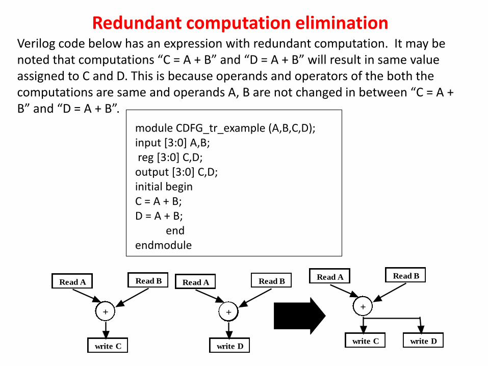
Redundant computation elimination Verilog code below has an expression with redundant computation. It may be noted that computations “C = A + B” and “D = A + B” will result in same value assigned to C and D. This is because operands and operators of the both the computations are same and operands A, B are not changed in between “C = A + B” and “D = A + B”.
Read A
+
write C
Read B Read A
+
write D
Read BRead A
+
write C
Read B
write D
module CDFG_tr_example (A,B,C,D); input [3:0] A,B; reg [3:0] C,D; output [3:0] C,D; initial begin C = A + B; D = A + B; end endmodule
Common Sub-computation elimination
If there are two expressions “assigned variable1=operand11 OPERATOR11 ……OPERATOR1n operand1n” and “assigned variable2=operand21 OPERATOR21 ….,OPERATOR2n operand2n” where, operand1k=operand2k, OPERATOR1k=OPERATOR2k,…., operand1m= operand2m and , and the operands operand1k, operand1(k+1),….. operand2m do not get modified in between evaluating “assigned variable1” and “assigned variable2”, then we can perform the sub-computation (i.e., “operand1k OPERATOR1k,…., OPERATOR1(k-1) operand2m”) only once for “assigned variable1” and use the value for “assigned variable2”. This reduction is called common sub-computation elimination. So, redundant computation elimination is a special case of common sub-computation elimination, where k=1 and m=n. Like redundant computation elimination, common sub-computation elimination also reduces hardware requirements.
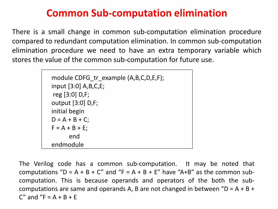
Common Sub-computation elimination
There is a small change in common sub-computation elimination procedure compared to redundant computation elimination. In common sub-computation elimination procedure we need to have an extra temporary variable which stores the value of the common sub-computation for future use.
module CDFG_tr_example (A,B,C,D,E,F); input [3:0] A,B,C,E; reg [3:0] D,F; output [3:0] D,F; initial begin D = A + B + C; F = A + B + E; end endmodule
The Verilog code has a common sub-computation. It may be noted that computations “D = A + B + C” and “F = A + B + E” have “A+B” as the common sub-computation. This is because operands and operators of the both the sub-computations are same and operands A, B are not changed in between “D = A + B + C” and “F = A + B + E
Common Sub-computation elimination
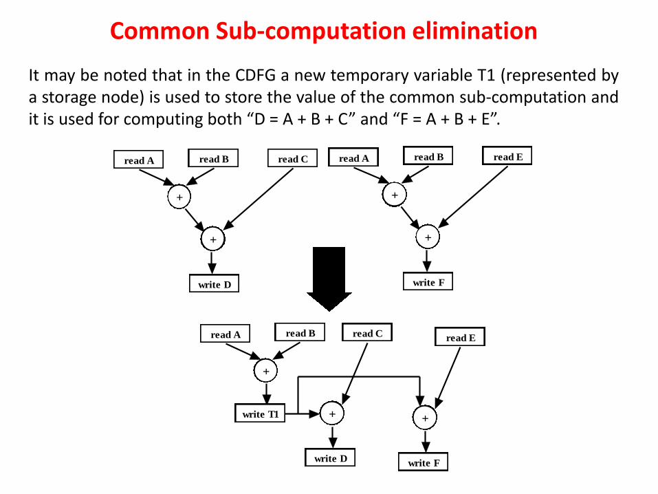
It may be noted that in the CDFG a new temporary variable T1 (represented by a storage node) is used to store the value of the common sub-computation and it is used for computing both “D = A + B + C” and “F = A + B + E”.
read Bread A
+
+
read C
write D
read Bread A
+
+
read E
write F
read Bread A
+
+
read C
write D
write T1 +
read E
write F
Dead-computation elimination
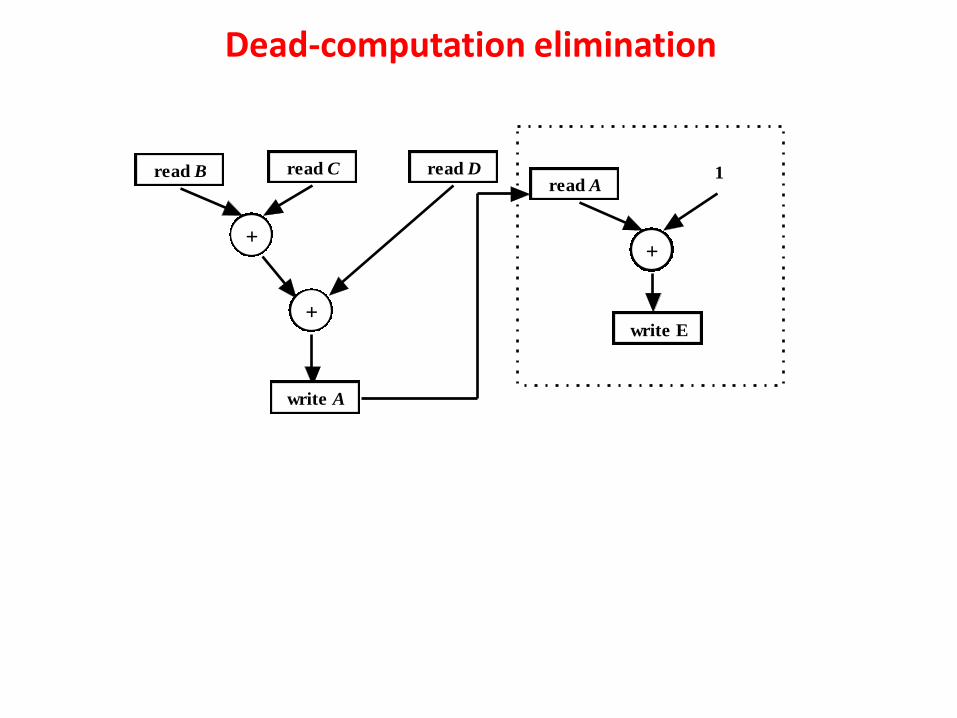
Dead-computation elimination is one of the most simple transformation where a computation that has no effect on the output of a code is eliminated. In the CDFG the corresponding nodes are eliminated.
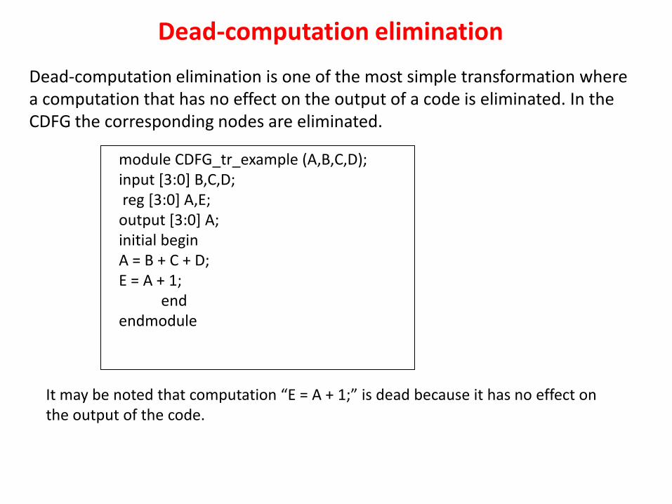
It may be noted that computation “E = A + 1;” is dead because it has no effect on the output of the code.
module CDFG_tr_example (A,B,C,D); input [3:0] B,C,D; reg [3:0] A,E; output [3:0] A; initial begin A = B + C + D; E = A + 1; end endmodule
Dead-computation elimination
read Cread B
+
+
read D
write A
+
write E
1read A
Flow-graph based transformations
In flow-graph based transformations the major objecting is to change the graph so that parallelism of the design can be explored. In this section, we will see two types of flow-graph transformations
•Tree height reduction based transformation •Control flow to data flow based transformation
Tree height reduction based transformation
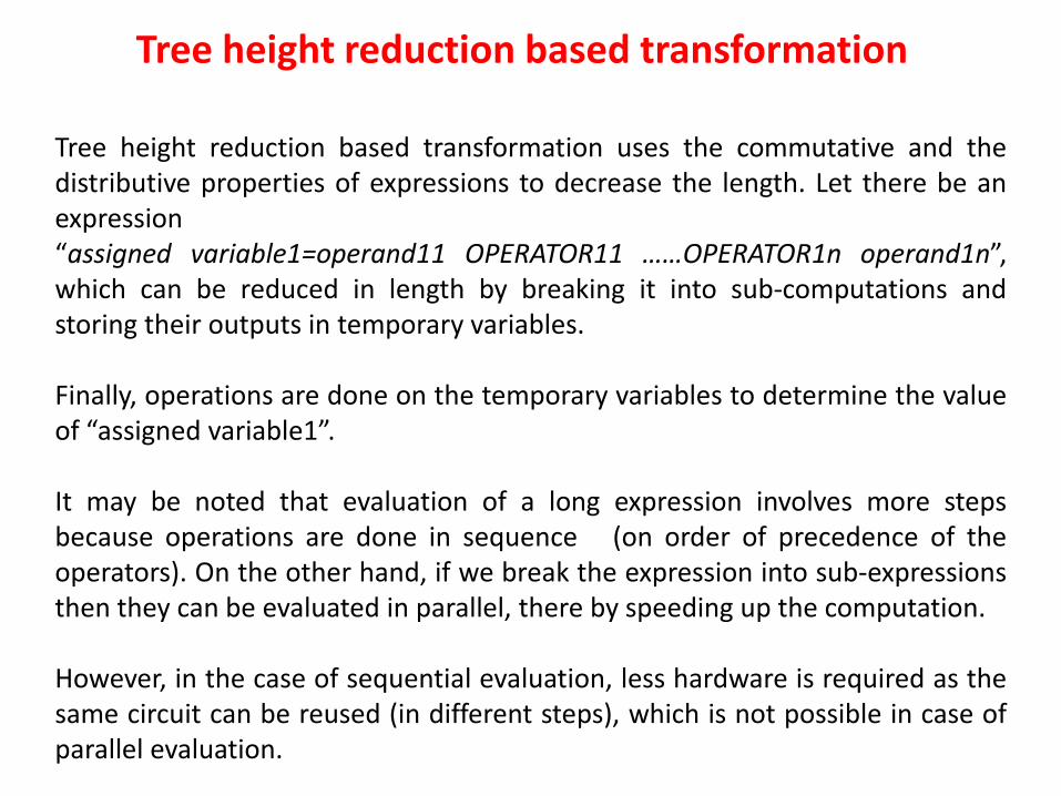
Tree height reduction based transformation uses the commutative and the distributive properties of expressions to decrease the length. Let there be an expression “assigned variable1=operand11 OPERATOR11 ……OPERATOR1n operand1n”, which can be reduced in length by breaking it into sub-computations and storing their outputs in temporary variables. Finally, operations are done on the temporary variables to determine the value of “assigned variable1”. It may be noted that evaluation of a long expression involves more steps because operations are done in sequence (on order of precedence of the operators). On the other hand, if we break the expression into sub-expressions then they can be evaluated in parallel, there by speeding up the computation. However, in the case of sequential evaluation, less hardware is required as the same circuit can be reused (in different steps), which is not possible in case of parallel evaluation.
Tree height reduction based transformation
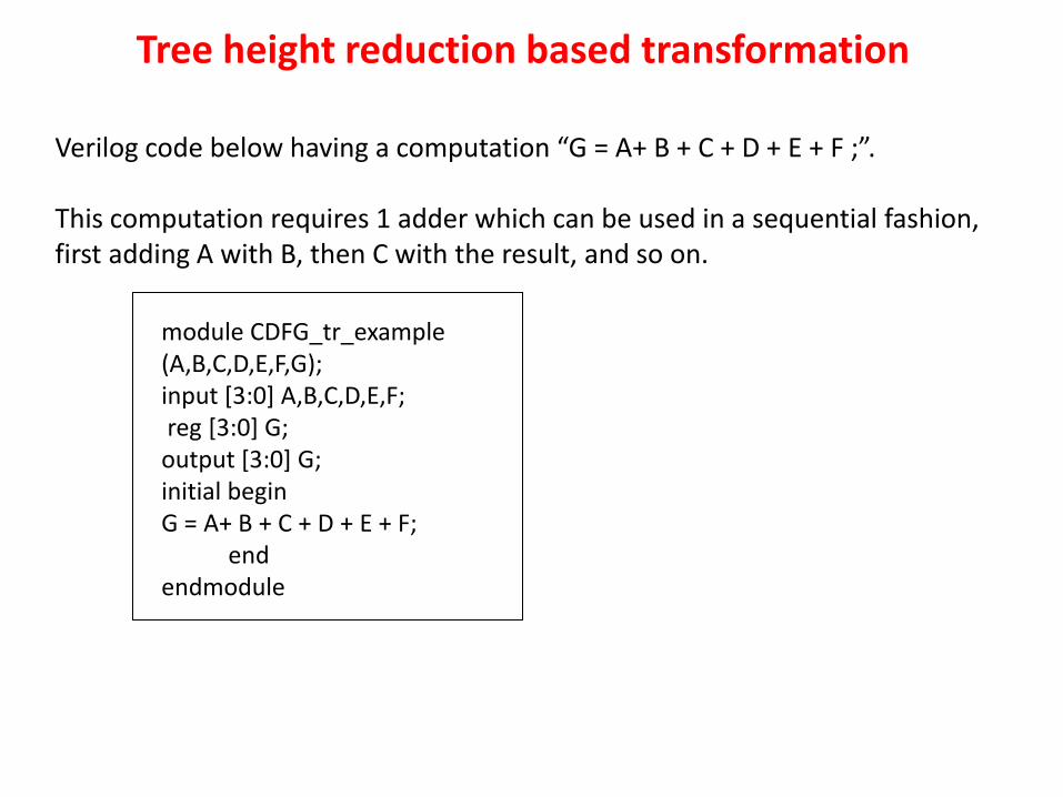
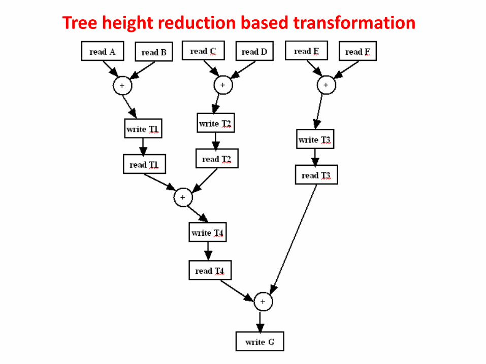
Verilog code below having a computation “G = A+ B + C + D + E + F ;”. This computation requires 1 adder which can be used in a sequential fashion, first adding A with B, then C with the result, and so on.
module CDFG_tr_example (A,B,C,D,E,F,G); input [3:0] A,B,C,D,E,F; reg [3:0] G; output [3:0] G; initial begin G = A+ B + C + D + E + F; end endmodule
Tree height reduction based transformation
Tree height reduction based transformation
Tree height reduction based transformation
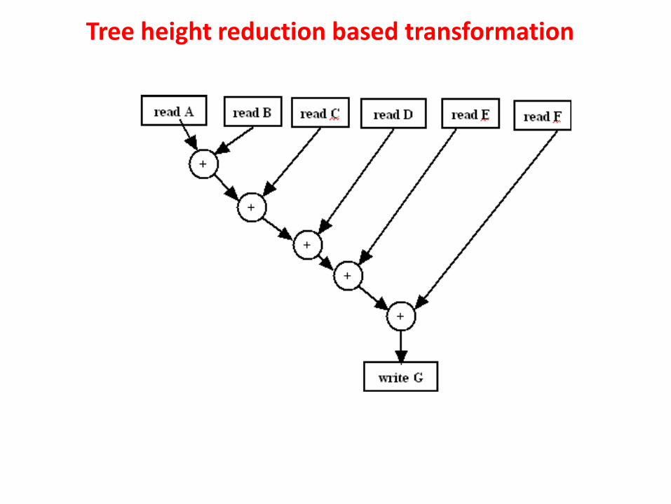
From the CDFG it may be noted that sequential computation requires 5 steps. Now, if we have more adders, then some of the sub-computations can be done in parallel; A+B, C+D and E+F can be done concurrently and results stored in three temporary variables. Finally G can be determined by adding the temporary variables. This parallel computation takes 3 steps.
CDFG: Control flow based representation
00 01 Default
read B read C
read D
write A
+
+
read B read C
read D
write A
-
-
read B read C
read D
write A
+
-
cond
CDFG: Control flow based representation
01 Default
read B
write A
read C read D
+
+
00
-
-
-
Hardware library based transformations
•Any operational node of a CDFG has a corresponding circuit capable of performing the operation e.g., adder to do addition, comparator for equality checking etc.
•This mapping of an operational node with hardware circuit depends on circuits available for implementation in the design library. For example, checking equality of a variable A (6 bit number say) with zero can be done using a 6-bit comparator or simply feeding all the 6 bits of A to an OR gate (if A is 0 then all the bits are 0 thereby generating 0 from the OR gate).
•The OR gate implementation consumes less hardware than the comparator, however, depends of availability of a 6 input OR gate in the library.
•Hardware library based transformations are modifications in the operational nodes of a CDFG, depending on availability of corresponding circuits in the design library, for achieving efficient circuit implementation in terms of area, frequency, power etc.
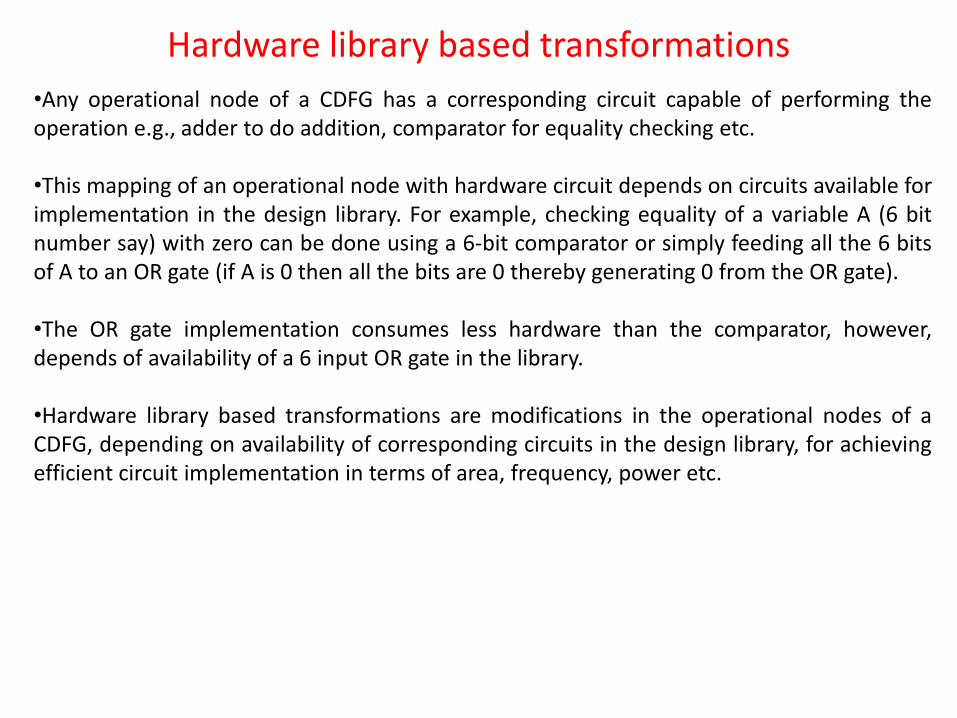
Hardware library based transformations
•Computation is “A=B+1”, involves an operational node for addition; this can be implemented using an adder where one operand is B and the other is 1.
• This computation can also be implemented using “INCR” circuit, which increments the input by 1. INCR block involves less resources than an adder.
•So, if the library has INCR block then CDFG can be transformed by replacing the adder operational node with INCR operational node
01 Default
write A
00
read B read C read D
+
1
+
01 Default
write A
00
read B read C read D
INCR+
Hardware library based transformations
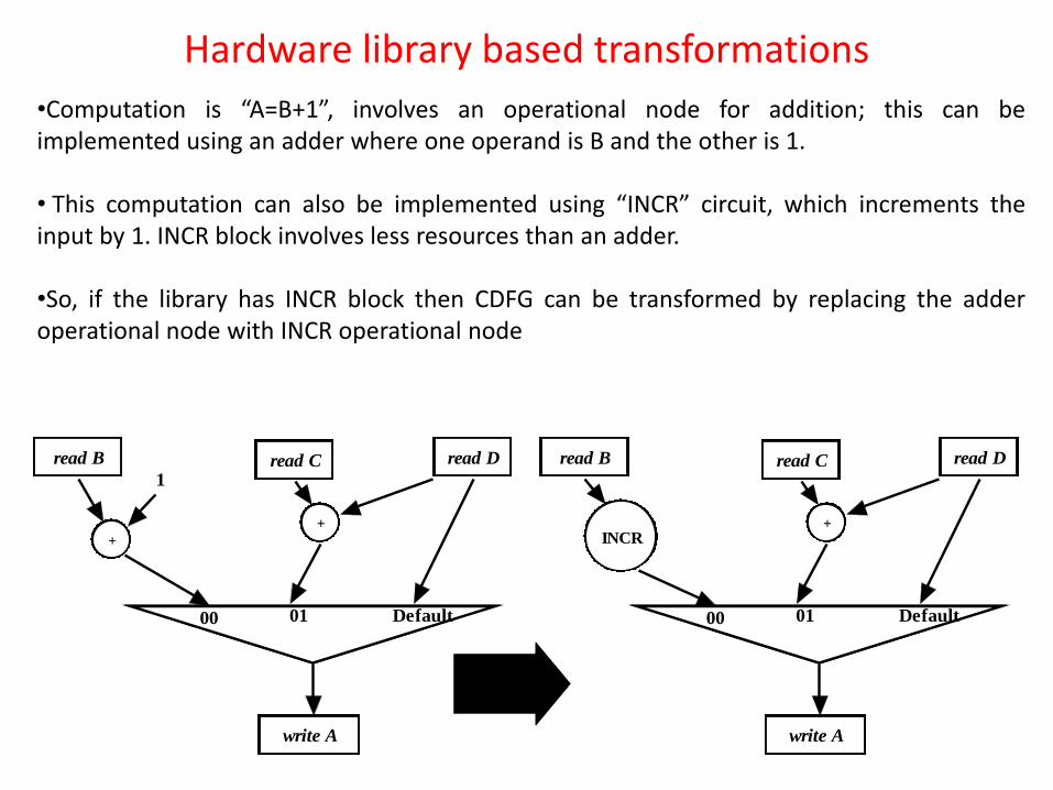
CDFG for computation “B=A*2”, involves an operational node for multiplication; this can be implemented using a multiplier where one operand is A and the other is 2. This computation can also be implemented using “left shift” circuit, which multiplies the input by 2. “Left shift” block is a shift register and therefore involves much less resources than a multiplier. So, if the library has “left shift” block then CDFG can be transformed by replacing the multiply operational node with “left shift” operational node
read A
X
2
write B
read A
<<
write B
left shift
Question and Answer
Question: After transformation of CDFGs and HDL codes, what step is required before processing them through HLS tools? After the CDFG / HDL code is transformed, it needs to be verified if their meaning (i.e., input-output behavior) remains same. In other words formal verification schemes are required to establish equivalence between the original and transformed CDFG/ HDL code. Although the techniques discussed above preserve equivalence, however, sometimes some parts of specifications may be missed resulting in behavioral difference. For example, sometimes dead-computations are kept in a loop to increase delay (for synchronization). If dead-code elimination is applied without looking into the timing specification then behavioral difference in terms of timing mismatch may occur.

Thank You