DESIGN SYNTHESIS AND MINIATURIZATION OF … · DESIGN SYNTHESIS AND MINIATURIZATION OF MULTIBAND...
218
DESIGN SYNTHESIS AND MINIATURIZATION OF MULTIBAND AND RECONFIGURABLE MICROSTRIP ANTENNA FOR FUTURE WIRELESS APPLICATIONS qi luo A Dissertation Submitted to Departamento de Engenharia Electrotécnica e de Computadores, Faculdade de Engenharia da Universidade do Porto in Partial Fulfillment of the Requirements for the Degree of Doctor of Philosophy July 2012
Transcript of DESIGN SYNTHESIS AND MINIATURIZATION OF … · DESIGN SYNTHESIS AND MINIATURIZATION OF MULTIBAND...

D E S I G N S Y N T H E S I S A N D M I N I AT U R I Z AT I O N O F M U LT I B A N DA N D R E C O N F I G U R A B L E M I C R O S T R I P A N T E N N A F O R
F U T U R E W I R E L E S S A P P L I C AT I O N S
qi luo
A Dissertation Submitted to Departamento de Engenharia Electrotécnica e deComputadores, Faculdade de Engenharia da Universidade do Porto in Partial
Fulfillment of the Requirements for the Degree of Doctor of Philosophy
July 2012

Qi Luo: Design Synthesis and Miniaturization of Multiband and Recon-figurable Microstrip Antenna for Future Wireless Applications, A Disser-tation Submitted to Departamento de Engenharia Electrotécnica e deComputadores, Faculdade de Engenharia da Universidade do Portoin Partial Fulfillment of the Requirements for the Degree of Doctor ofPhilosophy, © July 2012

T H E S I S I D E N T I F I C AT I O N
Title: Design Synthesis and Miniaturization of Multiband andReconfigurable Microstrip Antenna for Future Wireless
Applications
Keywords: Monopole Antenna, Fractal Antenna, Antenna Array,Electrically Small Antenna, Compact Antenna,
Reconfigurable Antenna, Artifical Magnetic Condutor
Start: November 2007
Duration: 4 years
Candidate information:
Name: Qi Luo
E-Mail: [email protected]
Curriculum Vitae: http://www.linkedin.com/in/luoqi
Supervisor information:
Name: Henrique Manuel de Castro Faria Salgado
E-Mail: [email protected]
Curriculum Vitae: http://www2.inescporto.pt/utm-en/author/hsalgado
Co-supervisor information:
Name: Jose Rocha Pereira
E-Mail: [email protected]
Curriculum Vitae: http://www.it.pt/person_detail_p.asp?id=468
Educational Establishment: Faculdade de Engenharia da Universidade doPorto-MAPTELE PhD Program
Research Institution: INESC Tech


S TAT E M E N T O F O R I G I N A L I T Y
The work presented in this thesis was carried out by the candidate.It has not been presented previously for any degree, nor is it presentunder consideration by any other degree awarding body.
Candidate:
(Qi Luo)
Principal Supervisor:
(Henrique Salgado)
Co-supervisor:
(Jose Rocha Pereira)


S TAT E M E N T O F AVA I L A B I L I T Y
I hereby give consent for my thesis, if accepted, to be available forphotocopying and for interlibrary loan, and for the title and summaryto be made available to outside organizatioins.
Candidate:
(Qi Luo)
Porto, Portugal, July 2012
vii

A B S T R A C T
This thesis is concerned with the design of compact multiband/re-configurable antennas and antenna arrays for wireless applications.
The size reduction of an antenna has an impact on its radiationperformance. Hence, methodologies for the design of compact sizeantennas with promising radiation characteristics are addressed inthis work by employing novel techniques for antenna miniaturizationbased on fractal geometries and by introducing lumped elements tothe printed monopole antenna design. Using fractal geometries threemultiband fractal monopole antennas, one fractal-based Inverted-Lantenna and one single feed fractal monopole antenna array are pre-sented. The experiment and simulation results of the proposed frac-tal antennas prove the advantages of fractal antennas, namely, com-pact size, multi-frequency operation and wide operation bandwidth.A second approach addressed in this work is the application of a tech-nique which includes a chip inductor into the antenna structure forthe purpose of reducing antenna size. By investigating the equivalentcircuit structure of the chip inductor, a design approach that involvesthe chip inductor to design a multiband antenna is proposed. Us-ing this methodology two electrically small antennas for dual bandWLAN as well as one compact antenna for multiband mobile com-munication that can cover almost the entire commercial available fre-quency bands were developed and their performances are discussed.
Moreover, the design of compact antenna arrays is also investigated.The approach discussed in this work to design compact multiband an-tenna arrays that contain closely space antennas, is to apply both theneutralizing and reconfigurable techniques on the printed monopoleantenna array. One compact size antenna array was developed for theWLAN 5.8 GHz USB dongle MIMO application. The other antennapresented is a reconfigurable compact dual band monopole antennaarray that can operate at each of the two WLAN frequency bandswhilst exhibiting high isolation. Additionally, innovative methods forthe design of reconfigurable antennas are also investigated. The ap-proach adopted to design the reconfigurable antenna is based on theconcept of active Artificial Magnetic Conductor ground plane. Herea new design is proposed using RF switches mounted on the surfaceof the AMC that consists of periodic square elements. After optimiza-tion, the resonant frequency of the coplanar antenna can be tuned byusing such an active AMC ground plane, whose reflection phase iscontrolled by the states of the RF switches.
These antennas have been implemented and characterized. The nu-merical simulations conducted in the Finite Element Method based
ix
electromagnetic simulation software package, Ansoft HFSS, are shownto match well with experimental results which proves the adequacyof the techniques devised.
R E S U M O
Esta Tese aborda o projecto de antenas compactas, multibanda e re-configuráveis para aplicações em comunicações sem fios.
A redução do tamanho duma antena tem um impacto negativono desempenho das suas características de radiação. Por consequên-cia, são abordadas nesta tese metodologias para projectar antenascom características de radiação promissoras empregando novas téc-nicas de miniaturização baseadas em geometrias fractais e na intro-dução de elementos discretos no projecto de antenas impressas dotipo monopolo. Usando geometrias fractais, apresentam-se aqui trêsantenas multibanda do tipo monopolo, uma Inverted-L Antenna eum agregado de duas antenas monopolo. Os resultados experimen-tais e os obtidos por simulação das antenas fractais propostas provamas vantagens destas antenas, nomeadamente no que diz respeito aotamanho compacto, à operação multifrequência e à grande largura debanda. Uma segunda abordagem usada neste trabalho é a utilizaçãode uma técnica que usa um elemento indutivo compacto inserido naestrutura da antena com o fim de reduzir o seu tamanho. Analisandoa estrutura do circuito equivalente do elemento indutivo, propõe-seuma abordagem adequada para o projecto de antenas multibandaque envolve a utilização destes elementos indutivos na implemen-tação de antenas de reduzida dimensão. Usando esta metodologiaforam desenvolvidas e analisadas duas antenas eletricamente peque-nas de banda dupla para WLAN, assim como uma antena compacta,para comunicações móveis multibanda, que pode cobrir quase todasas bandas de frequência comerciais disponíveis.
Além disso, foi também investigado o projecto de agregados deantenas compactos. A abordagem usada neste trabalho para projec-tar agregados de antenas multibanda compactos que contêm antenasmuito próximas, consistiu na aplicação das técnicas de neutralizaçãoe de reconfiguração a antenas impressas do tipo monopolo. Um agre-gado de antenas compacto, inserido num dispositivo dongle USB foidesenvolvido para uma aplicação MIMO WLAN a 5.8GHz. A outraantena aqui apresentada é um monopolo compacto reconfigurávele de banda dupla que pode operar em cada uma das duas bandasde frequências WLAN exibindo, mesmo assim, um isolamento ele-vado. Foram também investigados métodos inovadores para o pro-jeto de antenas reconfiguráveis. A abordagem adoptada para projetarestas antenas baseia-se no conceito de condutor magnético artificial,Artificial Magnetic Conductor (AMC). Por optimização a frequência
x

de ressonância da antena coplanar pode ser sintonizada usando esteAMC activo, cuja fase da reflexão é controlada pelo estado dos inter-ruptores de RF.
Todas as antenas foram construídas e caracterizadas. As simulaçõesnuméricas foram realizadas usando o software de simulação eletro-magnética HFSS da Ansoft baseado no Método dos Elementos Finitos(FEM). Obteve-se um bom acordo entre os resultados de simulação eexperimentais o que comprova a adequação das técnicas desenvolvi-das e utilizadas.
xi


A C K N O W L E D G M E N T S
It would not have been possible to write this doctoral thesis with-out the help and support of the kind people around me. First andforemost, I would like to thank my parents. Without out their love,support and encourage, I would not able to go abroad and accom-plish what I have done. I would also like to thank my girlfriend, YuXin Du, for her persistent support and encourage during these years.
I would like to express my appreciation to my supervisors, Prof.Henrique Salgado and Prof. Jose Rocha Pereira, for accepting me asa Ph.D student. I appreciate all their contributions of time and ad-vices to make my Ph.D experience productive and stimulating. With-out their continuous support, patience, enthusiasm, and motivation,I would not accomplish this work. Their guidance helped me in allthe time of research and writing of this thesis and I could not haveimagined having a better advisor and mentor for my Ph.D study.
Besides my supervisors, I would like to thank the rest of my the-sis committees, Prof. Artur Moura, Prof. Custódio Peixeiro, Prof. JoséRodrigues Rocha and Prof. Pedro Pinho, for their encouragement, in-sightful comments, and hard questions.
I would like to acknowledge the Fundação para a Ciência e a Tec-nologia (FCT), Portugal in the award of a PhD grant that providedthe necessary financial support for this research. I also would like tothank the staff at the Department of Electrical and Computer Engi-neering, University of Porto and Instituto de Telecomunicações (IT)Aveiro for their assistance and positive attitude. I would like to ex-press my thanks to Paulo Gonçalves and Carlos Graf for their help infabricating the antenna prototypes for my research work.
Last but not least, I wish to express my greatest thanks to thefriends and colleagues, who have supported and helped me duringmy staying in Portugal in the past five years. Their friendship is atreasure to me and without them, I could not enjoy my staying andhave such a nice life experience in Portugal.
xiii


C O N T E N T S
1 introduction 1
1.1 Motivation 1
1.2 Approach 3
1.2.1 Compact Multiband Antenna Design using Frac-tals 3
1.2.2 Antenna with Lumped Element 4
1.2.3 Neutralizing Techniques in Compact AntennaArray Design 5
1.2.4 Reconfigurable Techniques 6
1.3 Author’s Contributions 7
1.4 Thesis Overview 9
1.4.1 Part 1: Numerical Methods in Electromagnetic9
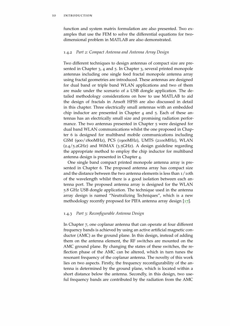
1.4.2 Part 2: Compact Antenna and Antenna ArrayDesign 10
1.4.3 Part 3: Reconfigurable Antenna Design 10
1.4.4 Conclusions and Future Work 11
i numerical methods in electromagnetics 13
2 numerical methods for electromagnetic compu-tation 15
2.1 Introduction 15
2.2 A Brief Review of Numerical Methods 15
2.2.1 Methods of Moments 15
2.2.2 Finite-Difference Time-Domain Method 17
2.2.3 Finite Element Method 18
2.2.4 Numerical Methods for Electrically Small An-tenna Design 20
2.3 Finite Element Method 21
2.3.1 FEM Analysis 21
2.3.2 Using FEM in 1D and 2D domain 29
2.3.3 Summary of the Chapter 36
ii compact antenna and antenna array design 39
3 fractal antenna design 41
3.1 Introduction 41
3.2 Basics of Fractal Geometry 41
3.3 Model Fractals in EM Simulation Tool with the Aid ofMATLAB 44
3.4 Multiband Fractal Monopole Antenna using MinkowskiIsland Geometry 51
3.4.1 Motivation 51
3.4.2 Antenna Design 52
xv

xvi contents
3.4.3 Simulated and Experimental Results 54
3.4.4 Antenna with Different Size of Ground Plane 57
3.4.5 Conclusion 58
3.5 Fractal Monopole Antenna for WLAN USB Dongle 59
3.5.1 Motivation 59
3.5.2 Antenna Design 60
3.5.3 Simulated and Experimental Results 62
3.5.4 Conclusion 63
3.6 Inverted-L Antenna (ILA) Design Using Fractal for WLANUSB Dongle 64
3.6.1 Motivation 64
3.6.2 Antenna Design 64
3.6.3 Simulated and Experimental Results 65
3.6.4 Antenna Performance Connected to a Laptop 69
3.6.5 Conclusions 71
3.7 Single Feed Fractal Monopole Antenna Array 73
3.7.1 Motivation 73
3.7.2 Antenna Design 74
3.7.3 Simulated and Measured Results 79
3.7.4 Proposed Antenna on a PDA Size Substrate 80
3.7.5 Conclusion 82
3.8 Summary of the Chapter 83
4 electrically small antenna design using chip
inductor 85
4.1 Introduction 85
4.2 Physical Limitations of Electrically Small Antenna 85
4.3 Simulation Model of Chip Inductor 88
4.4 Compact Printed C-shaped Monopole Antenna withChip Inductor 92
4.4.1 Motivation 92
4.4.2 Antenna Design 93
4.4.3 Simulated and Measured Results 94
4.4.4 Conclusion 101
4.5 Compact Printed Multi-Arm Monopole Antenna withChip Inductor for WLAN 102
4.5.1 Motivation 102
4.5.2 Antenna Structure 102
4.5.3 Simulated and Measured Results 104
4.5.4 Conclusion 109
4.6 Summary of the Chapter 109
5 printed monopole antenna for multiband mo-bile phone applications 111
5.1 Introduction 111
5.2 Motivation 111
5.3 Antenna Structure 112
5.4 Simulated and Measured Results 114

contents xvii
5.5 Antenna in Close Proximity to Human Head 120
5.6 Summary of the Chapter 123
6 compact printed monopole antenna array 125
6.1 Introduction 125
6.2 Performance Analysis of MIMO Antennas 125
6.2.1 Envelope Correlation Coefficient 125
6.2.2 Multi-Port Return Loss 128
6.3 Inverted-L Antennas Array in a Wireless USB Donglefor MIMO Application 129
6.3.1 Motivation 129
6.3.2 Antenna Design 130
6.3.3 Simulated and Measured Results 133
6.3.4 MIMO Performance Analysis 136
6.3.5 Conclusion 137
6.4 Summary of the Chapter 137
iii reconfigurable antenna design 139
7 tunable multiband antenna with an active ar-tificial magnetic conductor ground plane 141
7.1 Introduction 141
7.2 The Artificial Magnetic Conductor 141
7.3 Reconfigurable Antenna with Active AMC 146
7.3.1 Motivation 146
7.3.2 The Design of Active AMC Ground Plane 147
7.3.3 Design of Tunable Antenna on Active AMC GroundPlane 149
7.3.4 Simulated and Measured Results 150
7.3.5 Conclusion 154
7.4 Summary of the Chapter 154
8 reconfigurable dual-band monopole antenna ar-ray with high isolation 157
8.1 Introduction 157
8.2 Motivation 157
8.3 Single Band Compact Antenna Array For WLAN 2.4GHz 158
8.3.1 Antenna Structure 158
8.3.2 Simulated and Measured Results 160
8.4 Reconfigurable Dual-band Monopole Array With HighIsolation 164
8.4.1 Antenna Structure 164
8.4.2 Simulated and Measured Results 165
8.4.3 MIMO Performance Analysis 170
8.5 Summary of the Chapter 171
9 conclusion and future work 173
9.1 Conclusion 173
9.2 Future work 174

xviii contents
9.2.1 Electrically Small Antenna with 3D structure 174
9.2.2 Multiband Compact MIMO Antenna Array 176
bibliography 179

L I S T O F F I G U R E S
Figure 1 The evolution of the mobile communication stan-dards 1
Figure 2 The evolution of the Wireless LAN standards 2
Figure 3 Example of different standards that need to besupported by a future mobile phone 3
Figure 4 The general working flow of creating fractalsfor antenna modeling 4
Figure 5 The simplified circuit model of the chip induc-tor 5
Figure 6 Yee’s cell 18
Figure 7 Discretizing a block with triangular meshing 19
Figure 8 Linear discretization in one-dimensional domain 22
Figure 9 Triangular and Quadrilateral discretization intwo-dimensional domain (Meshing were gen-erated in MATLAB) 22
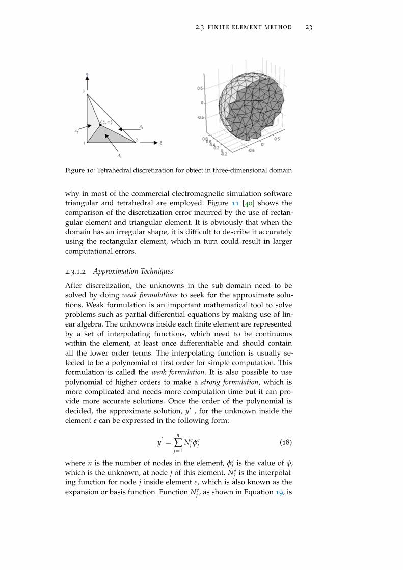
Figure 10 Tetrahedral discretization for object in three-dimensional domain 23
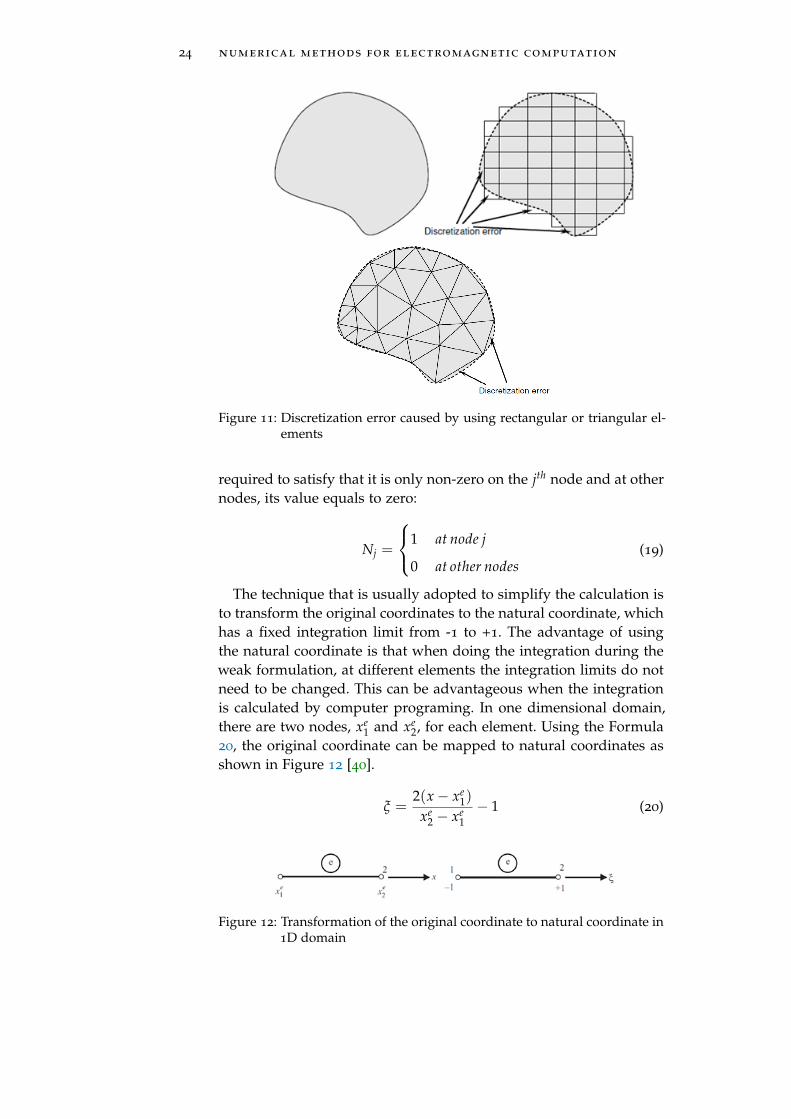
Figure 11 Discretization error caused by using rectangu-lar or triangular elements 24
Figure 12 Transformation of the original coordinate tonatural coordinate in 1D domain 24
Figure 13 Transformation of the triangular element to nat-ural coordinate 25
Figure 14 Transformation of the quadrilateral element tonatural coordinate 25
Figure 15 The local relationship of the nodes in 1-D do-main 28
Figure 16 The continuous condition of the domain usingtriangular finite element 29
Figure 17 A mesh with M linear elements in one-dimensionaldomain 30
Figure 18 The cross section of the joined coaxial waveg-uide at ρz plane 33
Figure 19 The subject domain with boundary conditions 34
Figure 20 The mesh of the domain and the calculatedelectric potential distribution. The unknownsinside the subject domain is meshed and solvedin MATLAB 34
Figure 21 Pseudo-code of the FEM programming in MAT-LAB 35
Figure 22 The rectangular box with metallic walls 35
xix
xx List of Figures
Figure 23 The plot of the mesh of the metallic box andthe calculated electric potential distribution byusing FEM 36
Figure 24 The first two iterations of the Koch Curve 43
Figure 25 The structure of Cantor set 43
Figure 26 A random version of the Koch Curve 44
Figure 27 Graph produced by formula iteration using Equa-tion 86 44
Figure 28 The 1st iteration of Koch Curve 45
Figure 29 The model of Koch Curve in the simulationtool 46
Figure 30 Process of design fractal geometries in simula-tion tool 47
Figure 31 Example of MATLAB coding to create vbs filefor designing fractal in HFSS 48
Figure 32 Interface of the MATLAB GUI tool for makingfractal geometries in HFSS 49
Figure 33 (a) Using GUI tool to make a vbs file for HilbertCurve of 3rd Iteration (b) The parameters listshown in HFSS after executing the vbs file (c)Top view of the Hilbert Curve in HFSS 49
Figure 34 (a) Using GUI tool to make a vbs file for de-signing a microstrip impedance match line us-ing the triangular taper technique; the impedanceof this microstrip line is transformed from 50
to 100 ohm (b) Top view of the designed mi-crostrip impedance line in HFSS 50
Figure 35 The 1st iteration and 2nd iteration of MinkowskiIsland geometry 52
Figure 36 Demonstration of the current cancellation ofmonopole design using the Hilbert Curve 53
Figure 37 The proposed fractal monopole antenna withgeometry of: (a) 1st iteration Minkowski Island;(b) 2nd iteration of Minkowski Island 54
Figure 38 The frequency ratio of the antenna with differ-ent value of d 54
Figure 39 Measured S11 of the proposed antenna withthe: (a) 1st iteration and (b) 2nd iteration ofMinkowski Island geometry 55
Figure 40 Simulated surface current distribution of themonopole antenna with the 1st iteration of MinkowskiIsland 56
Figure 41 Simulated surface current distribution of themonopole antenna with the 2nd iteration ofMinkowski Island 56
List of Figures xxi
Figure 42 Measured radiation pattern of the proposedantenna with 1st iteration Minkowski Islandat: (a) 2.4 GHz and (b) 5.2 GHz. Solid line rep-resents measured results on X-Z Plane whiledashed line represents measured results on X-Y plane 57
Figure 43 Measured radiation pattern of the proposedantenna with 2nd iteration Minkowski Islandat: (a) 2.4 GHz and (b) 5.2 GHz. Solid line rep-resents measured results on X-Z Plane whiledashed line represents measured results on X-Y plane 57
Figure 44 Simulated S11 of the proposed antenna: (a) with1st iteration Minkowski Island and (b) with2nd iteration Minkowski Island on ground planesof different size 58
Figure 45 The first three iterations of Cohen dipole 60
Figure 46 Top and bottom view of the proposed fractalmonopole antenna 61
Figure 47 (a) Top and (b) bottom view of the fabricatedfractal monopole 61
Figure 48 Measured S11 of the proposed USB fractal an-tenna 62
Figure 49 Simulated surface current distribution at 2.4,5.2 and 5.8 GHz of the proposed antenna 62
Figure 50 Measured radiation patterns at: (a) 2.4 GHzand (b) 5.2 GHz. Solid line represents mea-sured results on X-Z Plane (E-Plane) while dashedline represents measured results on X-Y plane(H-plane) 63
Figure 51 The structure of the previously designed an-tenna for WLAN USB Dongle 64
Figure 52 The proposed fractal ILA for WLAN USB Don-gle 65
Figure 53 Photo of the fabricated prototype during re-turn loss measurement 65
Figure 54 Comparison of the simulated and measuredS11 of the fractal ILA 66
Figure 55 Comparison of the measured S11 of the fractalILA and previously proposed fractal monopole 66
Figure 56 The structure of a typical Inverted-F antenna 66
Figure 57 Comparison of the simulated return loss be-tween the proposed fractal ILA and a typicalInverted-F antenna 67
Figure 58 The layout of the proposed antenna 68
xxii List of Figures
Figure 59 Parametrical studies for the proposed antenna:(a) simulated S11 of the antenna with differentvalue of L0; (b) simulated S11 of the antennawith different value of L1 68
Figure 60 Simulated S11of the antenna with different valueof L2 69
Figure 61 The frequency ratio of the antenna with differ-ent value of L1 (the length of L0 is fixed to 14
mm) 69
Figure 62 The simulation model of the fractal ILA con-necting to the laptop in HFSS 70
Figure 63 Simulated S11 of the proposed antenna withand without the laptop 70
Figure 64 Simulated S11 of the proposed antenna withlaptop computer of different length 71
Figure 65 Simulated radiation patterns of the proposedfractal ILA in free space and connected with alaptop computer 72
Figure 66 Structure of the 1st prototype fractal monopoleantenna array 74
Figure 67 The measured S11 of the 1st prototype of thedesigned single feed fractal antenna array 75
Figure 68 Proposed fractal antenna with different shapesof stubs on the ground plane: (a) Original de-sign; (b) Ground plane with rectangular shapestub; (c) Ground plane with circular shape stub;(d) Ground plane with triangular shape stub 76
Figure 69 Simulated S11 of the proposed antenna withdifferent stubs on the ground plane 76
Figure 70 Structure of the 2nd prototype fractal monopolearray antenna with improved impedance match77
Figure 71 Antenna with a L-Matching Network 77
Figure 72 The simulated input impedance of the frac-tal monopole array: (a) without using the pro-posed impedance match method; (b) with therectangular stub on the ground plane 78
Figure 73 The measured S11 of the fractal monopole an-tenna array with/out the proposed impedancematching method 79
Figure 74 Simulated 3D radiation pattern of the: (a) sin-gle feed fractal antenna array; (b) single fractalantenna 80
Figure 75 Top and side view of the proposed fractal monopolearray on a PDA size substrate 81

List of Figures xxiii
Figure 76 The measured and simulated S11 of the an-tenna array on a PDA size substrate 81
Figure 77 Measured radiation patterns of the proposedfractal array on the PDA size substrate. Thesolid line represents measured results on X-ZPlane (E-Plane) while dashed line representsmeasured results on X-Y plane (H-plane) 82
Figure 78 A dipole antenna enclosed in a sphere with ra-dius of a 86
Figure 79 The equivalent circuit structure of the chip in-ductor 88
Figure 80 Simplified equivalent circuit structure of thechip inductor 89
Figure 81 The value of equivalent series resistance andinductance of the chip inductor (Coilcraft 0402HP-20N) against frequency 90
Figure 82 The value of equivalent series resistance andinductance of the chip inductor (Coilcraft 0302CS-20NX) against frequency 90
Figure 83 Comparison of the calculated L( f ) for both chipinductors 91
Figure 84 Simulation model of the chip inductor in theEM simulation environment 91
Figure 85 (a) Top view, (b) Back view and (c) Side viewof the proposed C-shaped monopole antennawith embedded chip inductor 93
Figure 86 Simulated current distribution of the proposedC-shaped antenna at 2.4 GHz and 5.2 GHz 95
Figure 87 Simulated S11 of the proposed antenna withdifferent length of L3 and L4 96
Figure 88 Simulated S11 of the proposed antenna withdifferent length of L2 96
Figure 89 Simulated S11 of the proposed antenna withchip inductor in different locations on arm L3
97
Figure 90 Comparison between the measured and simu-lated S11 97
Figure 91 Comparison of the measured S11 between theproposed antenna with and without the chipinductor 98
Figure 92 Comparison of the return loss with new simu-lation model and measured result 98
Figure 93 Measured radiation pattern at X-Y plane (solidline) and X-Z plane (dashed line) at (a) 2.55GHzand (b) 5.25GHz 100

xxiv List of Figures
Figure 94 Simulated peak gain of the proposed antenna101
Figure 95 The top view of the proposed multi-arm monopoleantenna 104
Figure 96 Detailed view of the antenna radiation elementwith dimensions 104
Figure 97 Comparison between the simulated and mea-sured S11 of the proposed antenna 105
Figure 98 Simulated S11 of the proposed antenna withdifferent length of L3 105
Figure 99 Simulated S11 of the proposed antenna withdifferent length of L5 106
Figure 100 Simulated S11 of the proposed antenna withchip inductor in different positions 106
Figure 101 Simulated surface current distribution of theproposed antenna at 2.45 GHz (left) and 5.3GHz (right) 106
Figure 102 Measured E-plane (X-Z Plane) and H-plane (X-Y plane) radiation patterns of the proposed an-tenna at 2.45 GHz and 5.3 GHz 107
Figure 103 Simulated peak directivity and radiation effi-ciency of the proposed antenna at: (a)2.4 GHzband; (b)5.2 GHz band 108
Figure 104 Top and side view of the proposed multibandantenna 113
Figure 105 The main dimensions of the proposed antenna 113
Figure 106 The comparison between measured and simu-lated S11 of the proposed antenna 114
Figure 107 The comparison between the simulated S11 ofthe proposed antenna with and without thechip inductor 115
Figure 108 The simulated current distribution of the pro-posed antenna at: (a) 960 MHz; (b)1800 MHz;(c)1900 MHz; (d)2.4 GHz; (e)3.8 GHz and (f)5.25
GHz. The stronger current is represented bylighter colors 115
Figure 109 Simulated S11 of the proposed antenna whenchanging the length of L1 116
Figure 110 Simulated S11 of the proposed antenna whenchanging the length of L2 116
Figure 111 Simulated S11 of the proposed antenna whenchanging the length of L3 117
Figure 112 Simulated S11 of the proposed antenna whenchanging the length of L4 117
Figure 113 Simulated S11 of the proposed antenna whenchanging the length of L5 117

List of Figures xxv
Figure 114 Simulated S11of the proposed antenna with dif-ferent length of ground planes 118
Figure 115 Comparison of the simulated S11 of the pro-posed multiband antenna when placed in aplastic housing and in free space 118
Figure 116 Measured E-plane (X-Z Plane) and H-plane (X-Y plane) radiation patterns of the proposed multi-band antenna at: (a) 960MHz; (b) 1800MHz; (c)1900MHz; (d) 2.4GHz; (e) 3.5GHz; (f) 5.2GHz. 119
Figure 117 The simulation model of the proposed antennawith the human head 120
Figure 118 Comparison of the simulated S11 between theantenna with the head phantom and in the freespace 121
Figure 119 Simulated 3D radiation pattern of the proposedantenna with the human head phantom 122
Figure 120 Simulated SAR distribution on the head phan-tom for the proposed antenna at 960 MHz 123
Figure 121 The uncertainly of the calculated correlationcoefficient 128
Figure 122 The structure of a typical Inverted-L antenna 130
Figure 123 The layout of the WLAN USB dongle 130
Figure 124 The structure of the antenna array with neu-tralizing line 131
Figure 125 ILA with a L-shape stub 132
Figure 126 The structure of the proposed antenna array 132
Figure 127 Photo of the fabricated ILA array 133
Figure 128 Measured scattering parameters of the ILAs ar-ray 134
Figure 129 Comparison the simulated and measured re-turn loss and isolation of the proposed antennaarray 134
Figure 130 Simulated surface current distribution of theantenna array when Port 2 is excited 135
Figure 131 Comparison of the simulated S11 and S21 ofthe proposed antenna array with and withoutthe vertical stub on the neutralizing line 135
Figure 132 Comparison between the simulated and mea-sured radiation patterns of the proposed ILAsarray 136
Figure 133 Calculated envelope correlation coefficient ofthe proposed antenna array 137
Figure 134 Calculated TMRL of the proposed antenna ar-ray 137
Figure 135 Cavity model for the Artificial Magnetic Con-ductor 141

xxvi List of Figures
Figure 136 The propagation model when the source is lo-cated at a distance of d from the AMC 142
Figure 137 The plane wave with normal incident anglepropagates towards the AMC with impedanceof Zs(w) 143
Figure 138 Artificial Magnetic Conductor with square patcharrays 144
Figure 139 The effective surface impedance model of theAMC structure 144
Figure 140 The transmission line model of the AMC asa parallel connection of the PRS and a metal-backed dielectric slab 145
Figure 141 Top and side view of the AMC ground plane 147
Figure 142 (a): Demonstration of four unit cells aggregatedto one larger unit cell; (b): Demonstration of4×4 unit cells aggregated to 2×2 unit cells ofequivalent size 148
Figure 143 Reflection phase when the switches on the AMCsurface are ON (dotted line) and OFF (solidline); the results are exported from HFSS 148
Figure 144 (a) Top view of the coplanar patch antenna; (b)side view of the coplanar patch antenna 2 mmabove the AMC 149
Figure 145 Top view of the two fabricated AMC groundplane that mimic the case when the switcheson the AMC surface are perfectly switched (a)‘OFF’and (b) ‘ON’. 150
Figure 146 (a) Simulated and (b) Measured S11 of copla-nar antenna in free space and with the AMCground plane when the RF switches are OFF151
Figure 147 (a) Simulated and (b) Measured S11 of the pro-posed reconfigurable coplanar antenna whenthe RF switches are in ‘ON’ (dash line) and‘OFF’ (solid line) state. 152
Figure 148 Measured E-plane (X-Z Plane) and H-plane (X-Y plane) radiation patterns at: (a) 2.42 GHz, (b)5.2 GHz, (c) 4.5 GHz and (d) 5.9 GHz 153
Figure 149 (a)Top view, (b)back view and (c) side view ofthe proposed antenna array 159
Figure 150 The influence of the location of the neutraliz-ing line to the S11 and S21 for several value ofh 160
Figure 151 Simulated current distribution of the antennaarray: (a) with the neutralizing line; and (b)without the neutralizing line 161
Figure 152 Photos of the fabricated prototypes 161
Figure 153 Measured S12 of the C-shaped antenna arraywith and without the neutralizing line 162
Figure 154 Comparison of the measured and simulated:(a) S11 and (b) S21 of the proposed C-shapedantenna array 162
Figure 155 Measure S11 and S21 of the single band printedmonopole antenna array at 2.4 GHz 163
Figure 156 Measured radiation patterns at E plane (X-ZPlane) and H plane (X-Y Plane) of the pro-posed antenna array with port 1 excited andport 2 connected to a 50ohm load 163
Figure 157 Neutralizing line with two RF switches 164
Figure 158 The equivalent circuit structure when: (a) theRF switches are turned ON and (b) the RF switchesare turned OFF 165
Figure 159 The dimensions of the proposed monopole an-tenna array. The two slots on the neutralizingline are the positions for RF switches 165
Figure 160 Simulated S11 and S12 of the antenna arraywith RF switches on different locations withswitches in the ’OFF’ state 166
Figure 161 Current distribution at 2.4 GHz (right) whenthe RF switches are turned ’OFF’ and 5.2 GHz(left) when the RF switches are turned ’ON’167
Figure 162 Fabricated two antenna array prototypes on FR4
168
Figure 163 Measured S11 and S12 of the reconfigurableprinted monopole array at: (a) 2.4 and (b) 5.2GHzwhen the switches are turned ‘ON’ and ‘OFF’ 168
Figure 164 Simulated 3D radiation pattern of the proposedantenna array at 2.4 GHz and at 5.3 GHz 169
Figure 165 Calculated envelope correlation coefficient ofproposed antenna array: (a) At 2.4 GHz whenswitches are ‘ON’; (b) At 5.2 GHz when switchesare ‘OFF’ 170
Figure 166 Calculated TMRL against the S11 of the pro-posed antenna array 171
Figure 167 Two electrically small antennas designed forthe car key application at 868 MHz. (a) Design1, which has a planar structure; (b) Design 2,which has a 3D structure 175
Figure 168 The simulated return loss of both proposedelectrically small antennas 175
xxvii

xxviii List of Tables
L I S T O F TA B L E S
Table 1 The list of coordinates for the Koch Curve 45
Table 2 Parameters of the proposed antenna 94
Table 3 Calculated Q factor of the proposed antenna 101
Table 4 Summary of performance of the proposed printedmonopole antenna 109
Table 5 Simulated Peak gain and radiation efficiencyof the proposed antenna at each frequency band 120
Table 6 Simulated Peak gain of the proposed antennaat each frequency band 121
Table 7 Values of the parameters 132
Table 8 Summary of the radiation characteristics of theproposed antenna 153
Table 9 The quality (Q) factor of the designed two an-tennas 176

L I S T O F A C R O N Y M S
AC Alternating CurrentAMC Artificial Magnetic ConductorDC Direct CurrentDCS Digital Communications SystemDNG Double NegativeDVB Digital Video BroadcastingEBG Electromagnetic Band-GapEM ElectromagneticESA Electrically Small AntennaFDTD Finite-Difference Time-DomainFEM Finite Element MethodHFSS High Frequency Structure SimulatorHIP High Impedance SurfaceIEEE Institute of Electrical and Electronics EngineersIFA Inverted-F AntennaIFS Iterated Function SystemILA Inverted-L AntennaGPS Global Positioning SystemGUI Graphical User InterfaceGSM Global System for Mobile CommunicationsLTE Long Term EvolutionMIMO Multiple Input Multiple OutputMoM Method of MomentsMEMS Micro-electromechanical SystemsPCB Printed Circuit BoardPCS Personal Communications ServicePDA Personal Digital AssistantPEC Perfect Electrical ConductorPIFA Planar Inverted-F AntennaPMC Perfect Magnetic ConductorPRS Partial Reflection SurfaceQ Quality FactorRF Radio FrequencyRLC Resistor-Inductor-CapacitorSAR Specific Absorption RatioTMRL Total Multiport Return Loss
xxix

xxx List of Tables
UMTS Universal Mobile Telecommunications SystemUSB Universal Serial BusWiMAX Worldwide Interoperability for Microwave AccessWLAN Wireless Local Area NetworkWWAN Wireless Wide Area NetworkZOR Zeroth Order Resonator
1I N T R O D U C T I O N
1.1 motivation
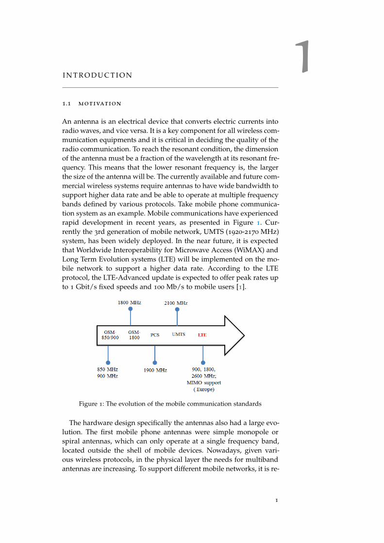
An antenna is an electrical device that converts electric currents intoradio waves, and vice versa. It is a key component for all wireless com-munication equipments and it is critical in deciding the quality of theradio communication. To reach the resonant condition, the dimensionof the antenna must be a fraction of the wavelength at its resonant fre-quency. This means that the lower resonant frequency is, the largerthe size of the antenna will be. The currently available and future com-mercial wireless systems require antennas to have wide bandwidth tosupport higher data rate and be able to operate at multiple frequencybands defined by various protocols. Take mobile phone communica-tion system as an example. Mobile communications have experiencedrapid development in recent years, as presented in Figure 1. Cur-rently the 3rd generation of mobile network, UMTS (1920-2170 MHz)system, has been widely deployed. In the near future, it is expectedthat Worldwide Interoperability for Microwave Access (WiMAX) andLong Term Evolution systems (LTE) will be implemented on the mo-bile network to support a higher data rate. According to the LTEprotocol, the LTE-Advanced update is expected to offer peak rates upto 1 Gbit/s fixed speeds and 100 Mb/s to mobile users [1].
Figure 1: The evolution of the mobile communication standards
The hardware design specifically the antennas also had a large evo-lution. The first mobile phone antennas were simple monopole orspiral antennas, which can only operate at a single frequency band,located outside the shell of mobile devices. Nowadays, given vari-ous wireless protocols, in the physical layer the needs for multibandantennas are increasing. To support different mobile networks, it is re-
1
2 introduction
quired to have the handset be equipped with an multiband antenna,a quad-band or even penta-band antenna for example, or multipleantennas. LTE requires Multiple Input Multiple Output (MIMO) tech-niques to be employed on the mobile devices [2]. In order to enableone mobile device to support all of these mobile wireless protocols,at the physical layer, it is essential to have one multiband antenna oreven an multiband antenna array integrated on this mobile device.
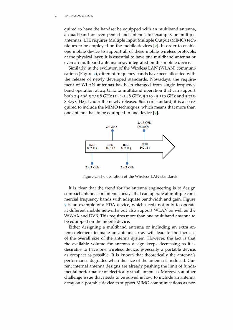
Similarly, in the evolution of the Wireless LAN (WLAN) communi-cations (Figure 2), different frequency bands have been allocated withthe release of newly developed standards. Nowadays, the require-ment of WLAN antennas has been changed from single frequencyband operation at 2.4 GHz to multiband operation that can supportboth 2.4 and 5.2/5.8 GHz (2.41-2.48 GHz, 5.250 - 5.350 GHz and 5.725-8.825 GHz). Under the newly released 802.11n standard, it is also re-quired to include the MIMO techniques, which means that more thanone antenna has to be equipped in one device [3].
Figure 2: The evolution of the Wireless LAN standards
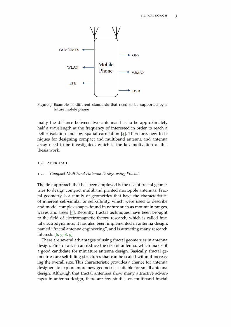
It is clear that the trend for the antenna engineering is to designcompact antennas or antenna arrays that can operate at multiple com-mercial frequency bands with adequate bandwidth and gain. Figure3 is an example of a PDA device, which needs not only to operateat different mobile networks but also support WLAN as well as theWiWAX and DVB. This requires more than one multiband antenna tobe equipped on the mobile device.
Either designing a multiband antenna or including an extra an-tenna element to make an antenna array will lead to the increaseof the overall size of the antenna system. However, the fact is thatthe available volume for antenna design keeps decreasing as it isdesirable to have one wireless device, especially a portable device,as compact as possible. It is known that theoretically the antenna’sperformance degrades when the size of the antenna is reduced. Cur-rent internal antenna designs are already pushing the limit of funda-mental performance of electrically small antennas. Moreover, anotherchallenge issue that needs to be solved is how to include an antennaarray on a portable device to support MIMO communications as nor-
1.2 approach 3
Figure 3: Example of different standards that need to be supported by afuture mobile phone
mally the distance between two antennas has to be approximatelyhalf a wavelength at the frequency of interested in order to reach abetter isolation and low spatial correlation [4]. Therefore, new tech-niques for designing compact and multiband antenna and antennaarray need to be investigated, which is the key motivation of thisthesis work.
1.2 approach
1.2.1 Compact Multiband Antenna Design using Fractals
The first approach that has been employed is the use of fractal geome-tries to design compact multiband printed monopole antennas. Frac-tal geometry is a family of geometries that have the characteristicsof inherent self-similar or self-affinity, which were used to describeand model complex shapes found in nature such as mountain ranges,waves and trees [5]. Recently, fractal techniques have been broughtto the field of electromagnetic theory research, which is called frac-tal electrodynamics; it has also been implemented in antenna design,named “fractal antenna engineering”, and is attracting many researchinterests [6, 7, 8, 9].
There are several advantages of using fractal geometries in antennadesign. First of all, it can reduce the size of antenna, which makes ita good candidate for miniature antenna design. Basically, fractal ge-ometries are self-filling structures that can be scaled without increas-ing the overall size. This characteristic provides a chance for antennadesigners to explore more new geometries suitable for small antennadesign. Although that fractal antennas show many attractive advan-tages in antenna design, there are few studies on multiband fractal
4 introduction
antenna design especially on its applications to printed monopole an-tennas. Therefore, this is a field that needs to be further explored.
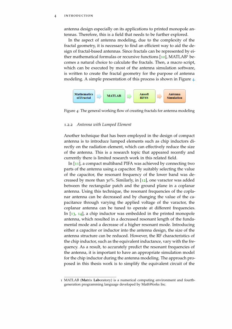
In the aspect of antenna modeling, due to the complexity of thefractal geometry, it is necessary to find an efficient way to aid the de-sign of fractal-based antennas. Since fractals can be represented by ei-ther mathematical formulas or recursive functions [10], MATLAB1 be-comes a natural choice to calculate the fractals. Then, a macro script,which can be executed by most of the antenna simulation software,is written to create the fractal geometry for the purpose of antennamodeling. A simple presentation of this process is shown in Figure 4.
Figure 4: The general working flow of creating fractals for antenna modeling
1.2.2 Antenna with Lumped Element
Another technique that has been employed in the design of compactantenna is to introduce lumped elements such as chip inductors di-rectly on the radiation element, which can effectively reduce the sizeof the antenna. This is a research topic that appeared recently andcurrently there is limited research work in this related field.
In [11], a compact multiband PIFA was achieved by connecting twoparts of the antenna using a capacitor. By suitably selecting the valueof the capacitor, the resonant frequency of the lower band was de-creased by more than 30%. Similarly, in [12], one varactor was addedbetween the rectangular patch and the ground plane in a coplanarantenna. Using this technique, the resonant frequencies of the copla-nar antenna can be decreased and by changing the value of the ca-pacitance through varying the applied voltage of the varactor, thecoplanar antenna can be tuned to operate at different frequencies.In [13, 14], a chip inductor was embedded in the printed monopoleantenna, which resulted in a decreased resonant length of the funda-mental mode and a decrease of a higher resonant mode. Introducingeither a capacitor or inductor into the antenna design, the size of theantenna structure can be reduced. However, the RF characteristics ofthe chip inductor, such as the equivalent inductance, vary with the fre-quency. As a result, to accurately predict the resonant frequencies ofthe antenna, it is important to have an appropriate simulation modelfor the chip inductor during the antenna modeling. The approach pro-posed in this thesis work is to simplify the equivalent circuit of the
1 MATLAB (Matrix Laboratory) is a numerical computing environment and fourth-generation programming language developed by MathWorks Inc.
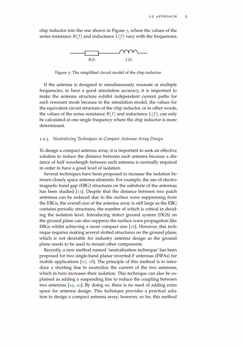
1.2 approach 5
chip inductor into the one shown in Figure 5, where the values of theseries resistance R( f ) and inductance L( f ) vary with the frequencies.
Figure 5: The simplified circuit model of the chip inductor
If the antenna is designed to simultaneously resonate at multiplefrequencies, to have a good simulation accuracy, it is important tomake the antenna structure exhibit independent current paths foreach resonant mode because in the simulation model, the values forthe equivalent circuit structure of the chip inductor, or in other words,the values of the series resistance R( f ) and inductance L( f ), can onlybe calculated at one single frequency where the chip inductor is moredeterminant.
1.2.3 Neutralizing Techniques in Compact Antenna Array Design
To design a compact antenna array, it is important to seek an effectivesolution to reduce the distance between each antenna because a dis-tance of half wavelength between each antenna is normally requiredin order to have a good level of isolation.
Several techniques have been proposed to increase the isolation be-tween closely space antenna elements. For example, the use of electro-magnetic band gap (EBG) structures on the substrate of the antennashas been studied [15]. Despite that the distance between two patchantennas can be reduced due to the surface wave suppressing fromthe EBGs, the overall size of the antenna array is still large as the EBGcontains periodic structures, the number of which is critical in decid-ing the isolation level. Introducing defect ground system (DGS) onthe ground plane can also suppress the surface wave propagation likeEBGs whilst achieving a more compact size [16]. However, this tech-nique requires making several slotted structures on the ground plane,which is not desirable for industry antenna design as the groundplane needs to be used to mount other components.
Recently, a new method named ‘neutralization technique’ has beenproposed for two single-band planar inverted-F antennas (PIFAs) formobile applications [17, 18]. The principle of this method is to intro-duce a shorting line to neutralize the current of the two antennas,which in turn increases their isolation. This technique can also be ex-plained as adding a suspending line to reduce the coupling betweentwo antennas [19, 20]. By doing so, there is no need of adding extraspace for antenna design. This technique provides a practical solu-tion to design a compact antenna array; however, so far, this method

6 introduction
has two limitations. Firstly, this technique has been employed only inthe PIFA antenna design. Secondly and more importantly, this tech-nique can only be applied to single band antenna arrays, yet there isincreasing need to have a multi-frequency antenna array.
This technique is further studied in this thesis work and has beensuccessfully applied to the design of a printed monopole antenna ar-ray. One major breakthrough that has been achieved is to introducethe reconfigurable concept into the neutralizing technique, which re-sults in a dual band compact printed monopole antenna array withhigh isolation.
1.2.4 Reconfigurable Techniques
Reconfigurable antennas are predicted to be one of the best candi-dates for future high data rate wireless communication systems [21].With the development of Microelectromechanical systems (MEMS)technologies, the fabrication of RF switches with good working per-formance become possible. Generally there are three methods to de-sign an reconfigurable antenna [22]:
1. Total geometry morphing, which employs a large amount ofswitchable sub-elements to form the desired antenna structure
2. Matching network morphing, which modifies the structure offeed and impedance matching network
3. Smart geometry morphing, which only modifies some impor-tant parameters of the antenna
The smart geometry morphing, which uses the minimum numberof switches, attracts most of the research interests. Work has beenconducted in this area, including the use of PIN diodes or MEMSin designing reconfigurable dipoles, slot antennas and stacked patchantennas [23, 24, 25].
Another approach that can be used to design reconfigurable an-tennas is to introduce varactor, whose capacitance varies with ap-plied voltage, into the antenna structure. One frequency reconfig-urable coplanar antenna [12] and patch antenna [26] were designedby adding one varactor between the antenna and its ground plane. Bychanging the value of the capacitance, the resonant frequency of bothantennas can be adjusted.
Materials that exhibit novel electromagnetic properties not found innature are attracting much attention of the research community. Suchstructures, known as metamaterials, are designed to have propertiesand operate in ways that bulk materials cannot. One example of suchmicrowave metamaterials are electromagnetic band-gap (EBG) struc-tures. These structures are playing a vital role to improve the perfor-mance of microwave components and antennas. Many researchers are
1.3 author’s contributions 7
using Metallic Electromagnetic Band Gap (MEBG) on antenna design.MEBG is composed by 2-D arrays of conducting elements immersedin the substrate. Generally, MEBG exhibits two unique characteristics:surface wave suppressing when used as EBG surface and in-phasereflection (90 degree to -90 degree) which can be used as an ArtificialMagnetic Conductor (AMC) [27]. In some literature, the second char-acteristic is also mentioned as High Impedance Surface (HIS) [28].
Recently, researchers found that when using the AMC as a groundplane for one antenna, it can to some degree influence the originalresonant frequency of the antenna. Therefore, the concept of using areconfigurable AMC structure to design reconfigurable antennas hasbeen studied [29, 30, 31]. Since EBG is a recent technology, improve-ments on present techniques for the design of microwave circuits andantennas are continuously being made. Great emphasis is presentlybeing given to the design of multiband AMCs and the use of recon-figurable or active AMC as the ground plane of a multiband antenna,which is also addressed in this thesis.
1.3 author’s contributions
The main contributions of this dissertation include:
• A method to use MATLAB to aid the modeling of the fractalantennas is proposed. This technique can be applied to mostof the EM simulation software packages. A small software toolhas been built in MATLAB by using the proposed method, withwhich several multiband printed fractal-based monopole anten-nas have been designed. These antennas have compact size andmulti-frequency operation characteristics. With the combinationof other antenna size reduction techniques such as meander line,the frequency ratio of the antenna can be better controlled.
• An equivalent simplified circuit model of the chip inductor,which is suitable to be introduced to the EM simulation soft-ware for antenna modeling, has been proposed. A methodologyof designing multiband antenna with chip inductor is also de-veloped. With the proposed method, the radiation performanceof the antenna can be accurately predicted. Two electrically smallmonopole antennas for dual band WLAN application and onemultiband printed monopole antenna that can support severalcommercial frequency bands, including GSM, UMTS, WLANand WiMAX, were proposed.
• A novel method that introduces the reconfigurable concept tothe neutralization technique is studied. It is demonstrated thatcompact printed monopole antenna arrays can be achieved byusing the neutralization technique. By introducing two RF switches

8 introduction
to the neutralization line, the design of compact dual band an-tenna arrays with high isolation can be achieved.
• A reconfigurable coplanar antenna is designed by using an ac-tive AMC ground plane. The frequency reconfiguration of theantenna is achieved by adding RF switches to the AMC groundplane, which itself behaves also as one additional radiation el-ements similar to a stacked antenna structure. This providesa new approach to design reconfigurable multi-frequency an-tenna.
This research work has resulted several publications on internationaljournals and conferences. The main publications are:
Journal Publications:
1. Qi Luo; J. R. Pereira and H.M. Salgado. Compact printed monopoleantenna with chip inductor for WLAN. IEEE Antennas and Wire-less Propagation Letters, 10:880-883, September 2011.
2. Q. Luo; J.R. Pereira and H.M. Salgado. Reconfigurable dualband C-shaped monopole antenna array with high isolation.Electronics Letters, 46(13):888-889, June 2010.
International Conferences:
1. Q. Luo; C. Quigley; J. Pereira and H. M Salgado. Inverted-L An-tennas Array in a Wireless USB Dongle for MIMO Application.In Proceedings of 6th European Conference on Antennas and Propa-gation (EuCAP), Prague, Czech Republic, March 2012.
2. Qi Luo; Jose Pereira and Henrique Salgado. Compact PrintedC-shaped Monopole Antenna With Chip Inductor. In Proceed-ings of IEEE International Symposium on Antennas and Propagation,Washington,USA, July 2011.
3. Qi Luo; H. M. Salgado and J. R. Pereira. Compact Printed MonopoleAntenna Array for Dual Band WLAN Application. In Proceed-ings of International Conference on Computer as a Tool (EUROCON),Lisbon, Portugal, November 2011.
4. Q. Luo; J.R. Pereira and H.M. Salgado. Tunable Multiband An-tenna With An Active Artificial Magnetic Conductor GroundPlane. In Proceedings of European Microwave Conference (EuMC),Paris, France, October 2010.
5. Q. Luo; H.M. Salgado and J.R. Pereira. Printed C-shaped MonopoleAntenna Array With High Isolation For MIMO Applications. InProceedings of IEEE Antennas and Propagation Society InternationalSymposium, Toronto, Canada, July 2010.

1.4 thesis overview 9
6. Q. Luo; H.M. Salgado and J.R. Pereira. Printed Fractal MonopoleAntenna Array For WLAN. In Proceedings of International Work-shop on Antenna Technology (iWAT), Lisbon, Portugal, March 2010.
7. Q. Luo; J.R. Pereira and H. Salgado. Fractal Monopole AntennaFor WLAN USB Dongle. In Proceedings of Loughborough Antennasand Propagation Conference, vol. 1, pp. 245-247, Loughborough,UK, November 2009.
8. Q. Luo; H. M. Salgado and J. R. Pereira. Fractal Monopole An-tenna Design Using Minkowski Island Geometry. In Proceed-ings of IEEE International Symposium on Antennas and Propagation,Charleston, United States, June 2009.
National Conferences:
1. Qi Luo; Jose Pereira and Henrique Salgado. Inverted-L Antenna(ILA) Design using Fractal for WLAN USB Dongle. In Proceed-ings of Conference on Electronics, Telecommunications and Comput-ers, Lisbon, Portugal, November 2011.
1.4 thesis overview
This thesis introduces several antenna and antenna array miniatur-ization techniques. The antennas proposed in this work are mainlydesigned for the application in WLAN and personal mobile commu-nications. This work is divided into three parts and the details of eachpart are outlined in the following sub-sections.
1.4.1 Part 1: Numerical Methods in Electromagnetic
An overview of the computational numerical methods is presentedin Chapter 2. The basics of three important numerical techniques,Method of Moment (MoM), Finite-Difference Time-Domain (FDTD)and Finite Element Method (FEM), are introduced. These three tech-niques have been widely employed by many electromagnetic simula-tion software packages for the design of different types of antennas.Considering the advantages and disadvantages of the above three nu-merical techniques, the method-of-choice of this thesis work is FEMmethod, which is more suitable to the design of compact and electri-cally small antennas that normally have a complicated structure andnarrow bandwidth. The main software that was used to simulate theantennas is Ansoft HFSS, which is a 3D EM simulator based on theFEM.
Although commercial software is available for antenna simulation,it is important to understand the theories of the numerical technique.In Chapter 2, the fundamental theory and mathematical derivationof FEM analysis including the domain discretization, interpolating
10 introduction
function and system matrix formulation are also presented. Two ex-amples that use the FEM to solve the differential equations for two-dimensional problem in MATLAB are also demonstrated.
1.4.2 Part 2: Compact Antenna and Antenna Array Design
Two different techniques to design antennas of compact size are pre-sented in Chapter 3, 4 and 5. In Chapter 3, several printed monopoleantennas including one single feed fractal monopole antenna arrayusing fractal geometries are introduced. These antennas are designedfor dual band or triple band WLAN applications and two of themare made under the scenario of a USB dongle application. The de-tailed methodology considerations on how to use MATLAB to aidthe design of fractals in Ansoft HFSS are also discussed in detailin this chapter. Three electrically small antennas with an embeddedchip inductor are presented in Chapter 4 and 5. Each of these an-tennas has an electrically small size and promising radiation perfor-mance. The two antennas presented in Chapter 5 were designed fordual band WLAN communications whilst the one proposed in Chap-ter 6 is designed for multiband mobile communications includingGSM (900/1800MHz), PCS (1900MHz), UMTS (2100MHz), WLAN(2.4/5.2GHz) and WiMAX (3.5GHz). A design guideline regardingthe appropriate method to employ the chip inductor for multibandantenna design is presented in Chapter 4.
One single band compact printed monopole antenna array is pre-sented in Chapter 6. The proposed antenna array has compact sizeand the distance between the two antenna elements is less than 1/10thof the wavelength whilst there is a good isolation between each an-tenna port. The proposed antenna array is designed for the WLAN5.8 GHz USB dongle application. The technique used in the antennaarray design is named “Neutralizing Techniques”, which is a newmethodology recently proposed for PIFA antenna array design [17].
1.4.3 Part 3: Reconfigurable Antenna Design
In Chapter 7, one coplanar antenna that can operate at four differentfrequency bands is achieved by using an active artificial magnetic con-ductor (AMC) as the ground plane. In this design, instead of addingthem on the antenna element, the RF switches are mounted on theAMC ground plane. By changing the states of these switches, the re-flection phase of the AMC can be altered, which in turn tunes theresonant frequency of the coplanar antenna. The novelty of this worklies on two aspects. Firstly, the frequency reconfigurability of the an-tenna is determined by the ground plane, which is located within ashort distance below the antenna. Secondly, in this design, two use-ful frequency bands are contributed by the radiation from the AMC

1.4 thesis overview 11
unit cells, which is an innovative method to make a multi-frequencyantenna.
One reconfigurable dual band compact monopole array is presentedin Chapter 8. This antenna array contains two C-shaped monopoleswith a shorting line, on which two RF switches were integrated, con-necting the two antenna elements that are separated by a distance of0.09λ2.4GHz. High isolation at 2.4 or 5.2 GHz bands can be achieved bychanging the states of the RF switches. By introducing the concept ofreconfigurability, it is demonstrated that one antenna array with twoclosely spaced antennas operating at WLAN dual frequency bandwith high isolation can be attained.
1.4.4 Conclusions and Future Work
Chapter 9 presents the conclusions of this thesis work as well as thefuture work that should be continually investigated in the scope ofcompact and electrically small multiband antenna and antenna arraydesign.


Part I
N U M E R I C A L M E T H O D S I NE L E C T R O M A G N E T I C S

2N U M E R I C A L M E T H O D S F O R E L E C T R O M A G N E T I CC O M P U TAT I O N
2.1 introduction
Nowadays, antenna design needs to employ numerical analysis tosolve the complex electromagnetic wave propagation, radiation andscattering problems, which are not always analytically calculable. Thesenumerical methods can be used to derive the closed form solutionof Maxwell’s equations by solving a large amount of integrations ordifferential equations. Thanks to the advances of the modern com-puter technologies, several commercial Electromagnetic (EM) simu-lators are available for antenna design. Generally speaking, there arethree main numerical methods that have been widely implemented inthe field of antenna simulation, namely Methods of Moments (MoM),Finite-Difference Time-Domain (FDTD) and Finite Element Method(FEM). The fundamental principles of these three popular computa-tional electromagnetic methods, MoM, FDTD and FEM, are brieflyintroduced in the Section2.2, where some discussions about the ad-vantages and disadvantages of each numerical method in the fieldof electrically small antenna simulation are also presented. More de-tailed discussion of the computational electromagnetic can be foundat [32, 33, 34].
Since the antennas presented in this thesis work were analyzed byusing Finite Element Method, it is important to understand the princi-ples of this numerical method for the purpose of better antenna mod-eling, which is the main objective of Section2.3. This section gives adetailed introduction of the FEM analysis in the order of the four ba-sic steps involved in a FEM analysis, namely domain discretization,interpolating function selection, system equations formulation andsolution of the system equations. Implementation of FEM to solveone-and two-dimensional problems are presented with some exam-ples that were solved with the aid of MATLAB. The discussion of theFEM analysis in the three-dimensional domain is not covered in thischapter due to the large computation complexity.
2.2 a brief review of numerical methods
2.2.1 Methods of Moments
Methods of Moments was first proposed by Harrington in 1968 [35].This method makes use of Maxwell’s equation in integration form
15
16 numerical methods for electromagnetic computation
to formulate the electromagnetic problems in terms of unknown cur-rents and calculates the coupling between the current elements basedon the Helmholtz-Equations:
4Φ + k20Φ = − ρ
ε0(1)
4−→A + k20−→A = −µ
−→J (2)
k0 = ω√
ε0µ0 (3)
where Φ represents the electrical potential, k0 is the free space wavenumber, ρ is the density of the electrical charge,
−→J is the current
vector,−→A is the magnetic vector potential, ε0 and µ0 is permittivity
and permeability of the free space, respectively. Using the definitionof potential functions, the
−→E and
−→H field can be calculated:
−→H =
1µ∇×−→A (4)
−→E = −jωµ
−→A −∇Φ (5)
With the help of the general solutions of the Helmholtz-Equations,and after mathematical derivation the coupling between each currentelement can be represented in the following form:
Uk =N
∑i=1
Zki Ii (6)
or
Z11 · · · Z1i · · · Z1N...
. . ....
Zk1 Zki ZkN...
. . ....
ZN1 · · · ZNi · · · ZNN
I1...
Ik...
IN
=
U1...
Uk...
UN
(7)
where Uk is the given source voltage, Zk is the coupling impedancematrix that describes the coupling relationship between each elementsand I is the unknown currents needed to be solved. After solvingthese linear equations, the current distribution on the conductive ma-terials can be calculated and then the other unknowns, for instancethe radiation pattern or return loss of one antenna, can be calculatedby post-processing.
The use of MoM technique usually leads to a dense matrix and thememory usage is proportional to the N2, where N is number of nodeswithin the subject domain after discretization. The MoM method issuitable to solve Perfect Electrical Conductor (PEC) objects, where the
2.2 a brief review of numerical methods 17
currents are only distributed on the surface. However, MoM will notbe an efficient method to solve problems that involves dielectrics andlayered structures in finite area. For example, in the software packageAdvanced Design System (ADS), during the antenna simulation italways considers an infinite substrate and ground plane and try toextract the current distribution on the substrate. This could lead to aninaccurate prediction when the antenna is designed on a substrate ofrelatively small size.
2.2.2 Finite-Difference Time-Domain Method
The FDTD method is based on the theory that the E-field and H-fieldare inter-related according the Maxwell’s differential equations: thetime derivative of the E-field is dependent on the curl of the H-fieldwhilst the time derivative of the H-field is dependent on the curl ofthe E-field:
∇×−→E = −µ∂−→H
∂t− σM
−→H (8)
∇×−→H = ε∂−→E
∂t+ σM
−→E (9)
In the Cartesian coordinate system, the above two equations can berewritten as the following six coupled partial differential equations:
∂Hx
∂t=
1µx
(∂Ey
∂z− ∂Ez
∂y− σMx Hx) (10)
∂Hy
∂t=
1µy
(∂Ez
∂x− ∂Ex
∂z− σMyHy) (11)
∂Hz
∂t=
1µz
(∂Ex
∂y−
∂Ey
∂x− σMzHz) (12)
∂Ex
∂t=
1εx(
∂Hz
∂y−
∂Hy
∂z− σxEx) (13)
∂Ey
∂t=
1εy(
∂Hx
∂z− ∂Hz
∂x− σyEy) (14)
∂Ez
∂t=
1εz(
∂Hy
∂x− ∂Hx
∂y− σzEz) (15)
In 1966, Yee [36] introduces the concept of “Yee cell” (Figure 6),which discretizes the computational domain into a rectangular grid.Based on this concept, using the FDTD method the E- and H-fieldcan be calculated step by step in a cyclic manner: the electric field issolved at a given instant in time, then the magnetic field is solved atthe next instant in time, and the process is repeated over and over
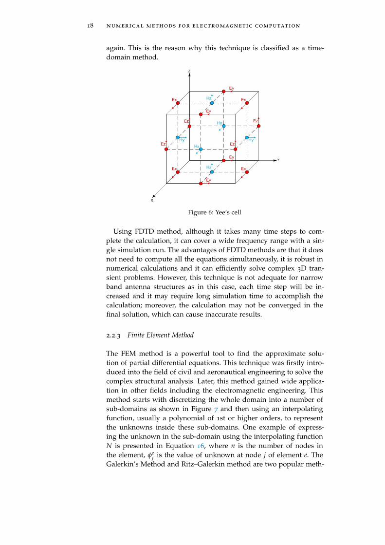
18 numerical methods for electromagnetic computation
again. This is the reason why this technique is classified as a time-domain method.
Figure 6: Yee’s cell
Using FDTD method, although it takes many time steps to com-plete the calculation, it can cover a wide frequency range with a sin-gle simulation run. The advantages of FDTD methods are that it doesnot need to compute all the equations simultaneously, it is robust innumerical calculations and it can efficiently solve complex 3D tran-sient problems. However, this technique is not adequate for narrowband antenna structures as in this case, each time step will be in-creased and it may require long simulation time to accomplish thecalculation; moreover, the calculation may not be converged in thefinal solution, which can cause inaccurate results.
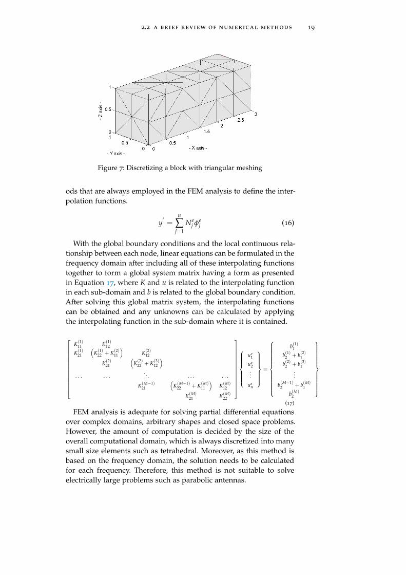
2.2.3 Finite Element Method
The FEM method is a powerful tool to find the approximate solu-tion of partial differential equations. This technique was firstly intro-duced into the field of civil and aeronautical engineering to solve thecomplex structural analysis. Later, this method gained wide applica-tion in other fields including the electromagnetic engineering. Thismethod starts with discretizing the whole domain into a number ofsub-domains as shown in Figure 7 and then using an interpolatingfunction, usually a polynomial of 1st or higher orders, to representthe unknowns inside these sub-domains. One example of express-ing the unknown in the sub-domain using the interpolating functionN is presented in Equation 16, where n is the number of nodes inthe element, φe
j is the value of unknown at node j of element e. TheGalerkin’s Method and Ritz–Galerkin method are two popular meth-
2.2 a brief review of numerical methods 19
Figure 7: Discretizing a block with triangular meshing
ods that are always employed in the FEM analysis to define the inter-polation functions.
y′=
n
∑j=1
Nej φe
j (16)
With the global boundary conditions and the local continuous rela-tionship between each node, linear equations can be formulated in thefrequency domain after including all of these interpolating functionstogether to form a global system matrix having a form as presentedin Equation 17, where K and u is related to the interpolating functionin each sub-domain and b is related to the global boundary condition.After solving this global matrix system, the interpolating functionscan be obtained and any unknowns can be calculated by applyingthe interpolating function in the sub-domain where it is contained.
K(1)11 K(1)
12
K(1)21
(K(1)
22 + K(2)11
)K(2)
12
K(2)21
(K(2)
22 + K(3)12
)· · · · · ·
. . . · · · · · ·K(M−1)
21
(K(M−1)
22 + K(M)11
)K(M)
12
K(M)21 K(M)
22
ue1
ue2...
uen
=
b(1)1
b(1)2 + b(2)1
b(2)2 + b(3)1...
b(M−1)2 + b(M)
1
b(M)2
(17)
FEM analysis is adequate for solving partial differential equationsover complex domains, arbitrary shapes and closed space problems.However, the amount of computation is decided by the size of theoverall computational domain, which is always discretized into manysmall size elements such as tetrahedral. Moreover, as this method isbased on the frequency domain, the solution needs to be calculatedfor each frequency. Therefore, this method is not suitable to solveelectrically large problems such as parabolic antennas.
20 numerical methods for electromagnetic computation
More discussions about FEM analysis can be found at Chapter 3,which is a chapter dedicated to the introduction of FEM method.
2.2.4 Numerical Methods for Electrically Small Antenna Design
Electrically small antenna refers to an antenna whose maximum di-mension is much smaller than its corresponding free space wave-length at its resonant frequency. To design an electrically small an-tenna, techniques that employ antenna of irregular shapes, substratewith non-homogeneous properties or multiple layers have been pro-posed. In this case, it is not suitable to simulate such structures us-ing the MoM as the antenna is confined in limited space and hasa non-planar structure or inhomogeneous substrate. An electricallysmall antenna usually has a narrow bandwidth since there is alwaysa trade-off between the antenna size and operation bandwidth/ef-ficiency/gain. The use of FDTD method to analyze such antennaswould take a long sequence of time steps to complete because thismethod is based on the time domain, which is inversely proportionalto the frequency domain. However, it is necessary to point out thatseveral commercial EM simulation software packages have integratedother techniques to overcome such limits and improve the calculationefficiency as well as accuracy of the original methods. For instance,the fast multiple method (FMM) has been applied to accelerate theiterative solver of MoM and the Finite integration technique (FIT) hasbeen developed to incorporate with the FDTD analysis.
Compared to the MoM and FDTD methods, FEM is naturally suit-able to model antennas of compact size and complicated structure.The computation of FEM is carried out in frequency domain and theamount of equations only depends on the total amount of the meshgenerated, which is proportional to the size of the domain needed tobe solved. Moreover, FEM is capable of solving antenna of arbitraryshape or within an inhomogeneous media. The objective of this re-search is to investigate the techniques for multiband antenna minia-turization and the antennas designed in this thesis work will be ofcompact size or electrically small. Moreover, the shapes of the anten-nas will have complex geometry (e.g. fractal) and substrates of highpermittivity might be used. Therefore, comparing the pros and consof the above three numerical techniques, the method-of-choice of thisthesis work layed on the FEM method. The main software chosen tosimulate the antennas is Ansoft HFSS, which is a 3D EM simulatorbased on the FEM.

2.3 finite element method 21
2.3 finite element method
2.3.1 FEM Analysis
The Finite Element Method (FEM) is a numerical technique to obtainapproximate solution of partial differential equations and integralequations. It can be used to derive the accurate solutions for com-plex engineering problems such as aircraft and car structural prob-lems. This method was proposed in 1940s and began to be employedin the field of airframe and structure analysis the 1950s. Nowadays,the FEM has been well established and widely used in various fieldsincluding mechanical, civil and aeronautical engineering as well aselectromagnetic.
The finite element method is considered to be one of the best meth-ods that can efficiently solve a wide variety of practical problems. Theprinciple behind this method is to discretize the subject domain intosmaller sub-domains, referred as the finite elements, and then useinterpolating functions to approximate the unknowns inside them.These sub-domains contain certain amount of nodes depending onthe employed discretization method. The triangular element is a typi-cal choice for solving 2-D problems and the use of tetrahedral elementis common for solving 3-D problems. The primary unknown will besolved inside these finite elements and the accuracy of the final solu-tion depends on the order of the interpolation functions used, whichmay be polynomials with first or higher orders. In the last step, thesefunctions will form a global matrix system with the internal relation-ships between the nodes and the values at the edges. After applyingthe global boundary conditions, the solutions can be obtained by solv-ing this global matrix system of equations.
One of the main advantages of this method is that once the gen-eral mathematical model has been built, which is normally writtenin computer code due to the large computation effort required, it canbe utilized to solve other similar problems by simply changing theinput data (such as the coefficients of the differential equation) andapplying suitable boundary conditions.
In the field of microwave and electromagnetics, the finite elementmethod was introduced by Silvester in 1969 [37]. After that, therewere a tremendous amount of researches that had been carried outand since 1970s, the finite element method started to be applied inthe analysis and design of various antennas [38]. Generally speaking,there are four basic steps included in a finite element analysis [39]:
• Discretization or subdivision of the domain
• Selection of the interpolation function
• Formulation of the system equations
22 numerical methods for electromagnetic computation
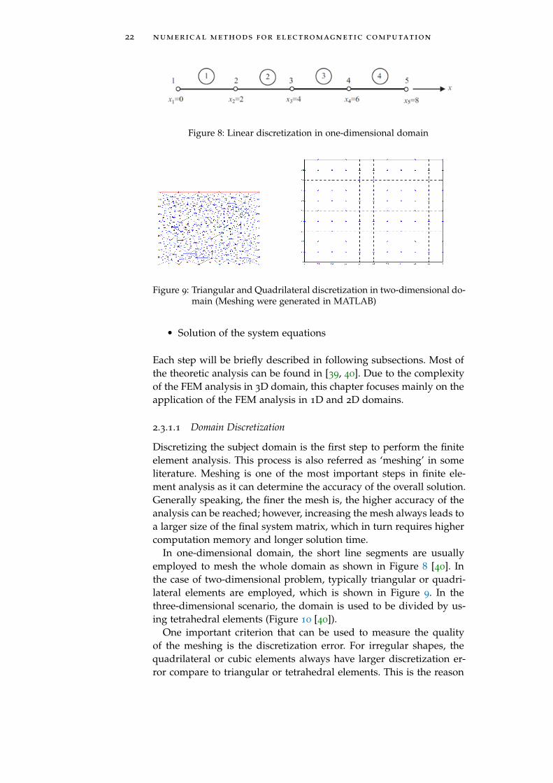
Figure 8: Linear discretization in one-dimensional domain
Figure 9: Triangular and Quadrilateral discretization in two-dimensional do-main (Meshing were generated in MATLAB)
• Solution of the system equations
Each step will be briefly described in following subsections. Most ofthe theoretic analysis can be found in [39, 40]. Due to the complexityof the FEM analysis in 3D domain, this chapter focuses mainly on theapplication of the FEM analysis in 1D and 2D domains.
2.3.1.1 Domain Discretization
Discretizing the subject domain is the first step to perform the finiteelement analysis. This process is also referred as ‘meshing’ in someliterature. Meshing is one of the most important steps in finite ele-ment analysis as it can determine the accuracy of the overall solution.Generally speaking, the finer the mesh is, the higher accuracy of theanalysis can be reached; however, increasing the mesh always leads toa larger size of the final system matrix, which in turn requires highercomputation memory and longer solution time.
In one-dimensional domain, the short line segments are usuallyemployed to mesh the whole domain as shown in Figure 8 [40]. Inthe case of two-dimensional problem, typically triangular or quadri-lateral elements are employed, which is shown in Figure 9. In thethree-dimensional scenario, the domain is used to be divided by us-ing tetrahedral elements (Figure 10 [40]).
One important criterion that can be used to measure the qualityof the meshing is the discretization error. For irregular shapes, thequadrilateral or cubic elements always have larger discretization er-ror compare to triangular or tetrahedral elements. This is the reason
2.3 finite element method 23
Figure 10: Tetrahedral discretization for object in three-dimensional domain
why in most of the commercial electromagnetic simulation softwaretriangular and tetrahedral are employed. Figure 11 [40] shows thecomparison of the discretization error incurred by the use of rectan-gular element and triangular element. It is obviously that when thedomain has an irregular shape, it is difficult to describe it accuratelyusing the rectangular element, which in turn could result in largercomputational errors.
2.3.1.2 Approximation Techniques
After discretization, the unknowns in the sub-domain need to besolved by doing weak formulations to seek for the approximate solu-tions. Weak formulation is an important mathematical tool to solveproblems such as partial differential equations by making use of lin-ear algebra. The unknowns inside each finite element are representedby a set of interpolating functions, which need to be continuouswithin the element, at least once differentiable and should containall the lower order terms. The interpolating function is usually se-lected to be a polynomial of first order for simple computation. Thisformulation is called the weak formulation. It is also possible to usepolynomial of higher orders to make a strong formulation, which ismore complicated and needs more computation time but it can pro-vide more accurate solutions. Once the order of the polynomial isdecided, the approximate solution, y′ , for the unknown inside theelement e can be expressed in the following form:
y′=
n
∑j=1
Nej φe
j (18)
where n is the number of nodes in the element, φej is the value of φ,
which is the unknown, at node j of this element. Nej is the interpolat-
ing function for node j inside element e, which is also known as theexpansion or basis function. Function Ne
j , as shown in Equation 19, is
24 numerical methods for electromagnetic computation
Figure 11: Discretization error caused by using rectangular or triangular el-ements
required to satisfy that it is only non-zero on the jth node and at othernodes, its value equals to zero:
Nj =
1 at node j
0 at other nodes(19)
The technique that is usually adopted to simplify the calculation isto transform the original coordinates to the natural coordinate, whichhas a fixed integration limit from -1 to +1. The advantage of usingthe natural coordinate is that when doing the integration during theweak formulation, at different elements the integration limits do notneed to be changed. This can be advantageous when the integrationis calculated by computer programing. In one dimensional domain,there are two nodes, xe
1 and xe2, for each element. Using the Formula
20, the original coordinate can be mapped to natural coordinates asshown in Figure 12 [40].
ξ =2(x− xe
1)
xe2 − xe
1− 1 (20)
Figure 12: Transformation of the original coordinate to natural coordinate in1D domain
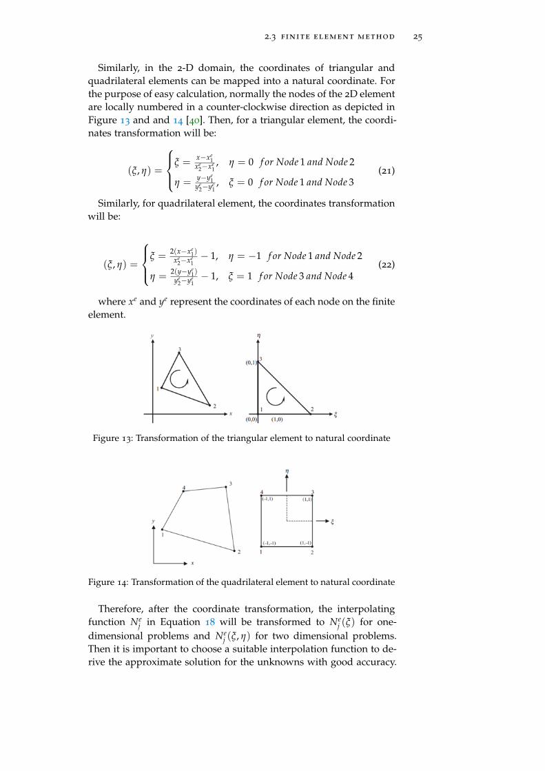
2.3 finite element method 25
Similarly, in the 2-D domain, the coordinates of triangular andquadrilateral elements can be mapped into a natural coordinate. Forthe purpose of easy calculation, normally the nodes of the 2D elementare locally numbered in a counter-clockwise direction as depicted inFigure 13 and and 14 [40]. Then, for a triangular element, the coordi-nates transformation will be:
(ξ, η) =
ξ =x−xe
1xe
2−xe1, η = 0 f or Node 1 and Node 2
η =y−ye
1ye
2−ye1, ξ = 0 f or Node 1 and Node 3
(21)
Similarly, for quadrilateral element, the coordinates transformationwill be:
(ξ, η) =
ξ =2(x−xe
1)xe
2−xe1− 1, η = −1 f or Node 1 and Node 2
η =2(y−ye
1)ye
2−ye1− 1, ξ = 1 f or Node 3 and Node 4
(22)
where xe and ye represent the coordinates of each node on the finiteelement.
Figure 13: Transformation of the triangular element to natural coordinate
Figure 14: Transformation of the quadrilateral element to natural coordinate
Therefore, after the coordinate transformation, the interpolatingfunction Ne
j in Equation 18 will be transformed to Nej (ξ) for one-
dimensional problems and Nej (ξ, η) for two dimensional problems.
Then it is important to choose a suitable interpolation function to de-rive the approximate solution for the unknowns with good accuracy.
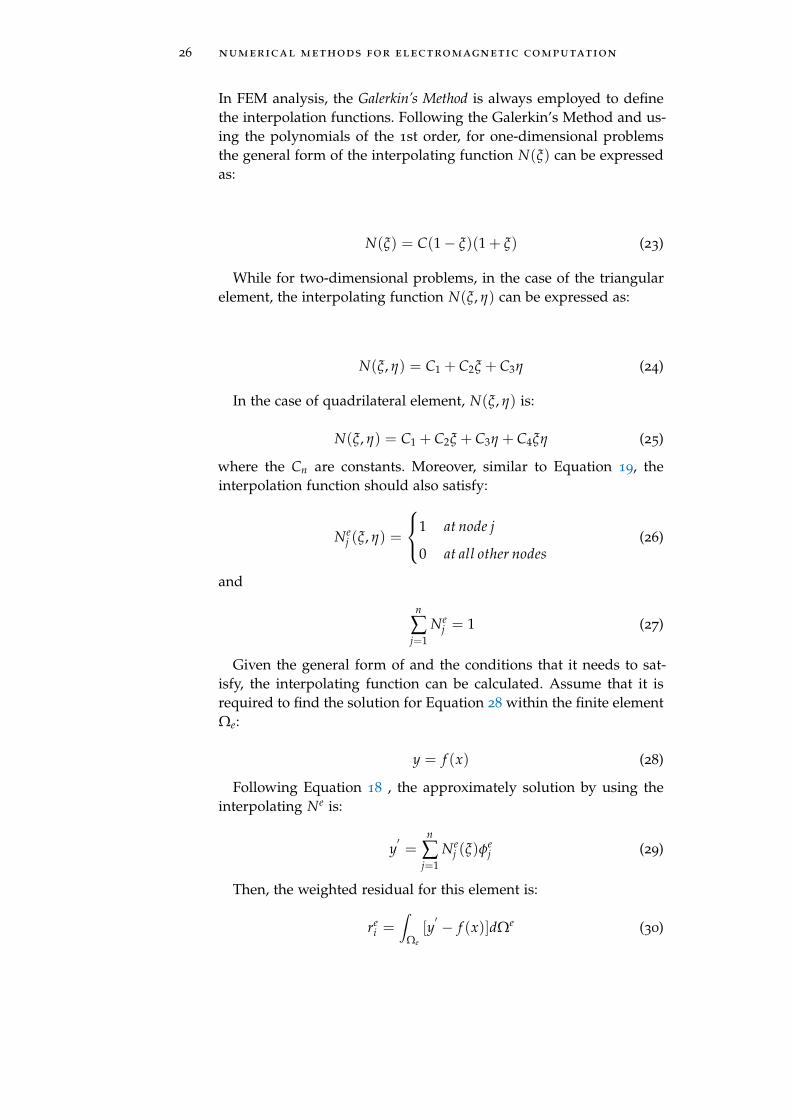
26 numerical methods for electromagnetic computation
In FEM analysis, the Galerkin’s Method is always employed to definethe interpolation functions. Following the Galerkin’s Method and us-ing the polynomials of the 1st order, for one-dimensional problemsthe general form of the interpolating function N(ξ) can be expressedas:
N(ξ) = C(1− ξ)(1 + ξ) (23)
While for two-dimensional problems, in the case of the triangularelement, the interpolating function N(ξ, η) can be expressed as:
N(ξ, η) = C1 + C2ξ + C3η (24)
In the case of quadrilateral element, N(ξ, η) is:
N(ξ, η) = C1 + C2ξ + C3η + C4ξη (25)
where the Cn are constants. Moreover, similar to Equation 19, theinterpolation function should also satisfy:
Nej (ξ, η) =
1 at node j
0 at all other nodes(26)
and
n
∑j=1
Nej = 1 (27)
Given the general form of and the conditions that it needs to sat-isfy, the interpolating function can be calculated. Assume that it isrequired to find the solution for Equation 28 within the finite elementΩe:
y = f (x) (28)
Following Equation 18 , the approximately solution by using theinterpolating Ne is:
y′=
n
∑j=1
Nej (ξ)φ
ej (29)
Then, the weighted residual for this element is:
rei =
∫Ωe
[y′ − f (x)]dΩe (30)
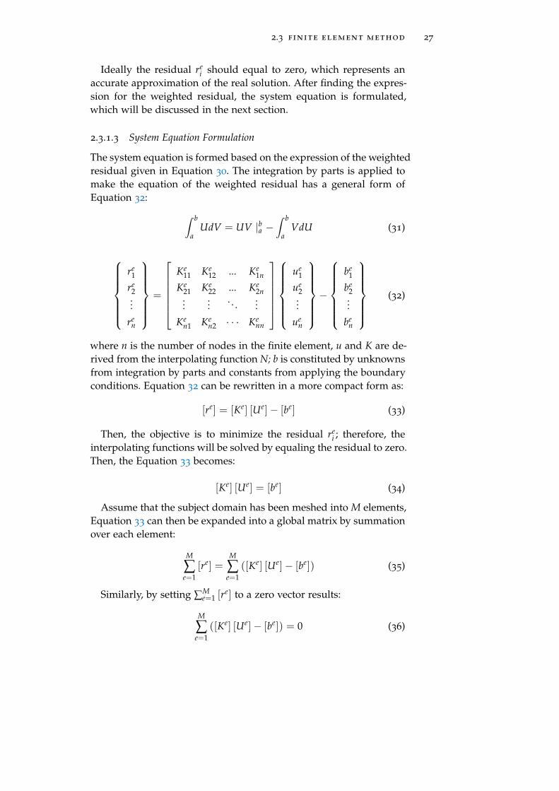
2.3 finite element method 27
Ideally the residual rei should equal to zero, which represents an
accurate approximation of the real solution. After finding the expres-sion for the weighted residual, the system equation is formulated,which will be discussed in the next section.
2.3.1.3 System Equation Formulation
The system equation is formed based on the expression of the weightedresidual given in Equation 30. The integration by parts is applied tomake the equation of the weighted residual has a general form ofEquation 32: ∫ b
aUdV = UV |ba −
∫ b
aVdU (31)
re
1
re2...
ren
=
Ke
11 Ke12 ... Ke
1n
Ke21 Ke
22 ... Ke2n
......
. . ....
Ken1 Ke
n2 · · · Kenn
ue
1
ue2...
uen
−
be
1
be2...
ben
(32)
where n is the number of nodes in the finite element, u and K are de-rived from the interpolating function N; b is constituted by unknownsfrom integration by parts and constants from applying the boundaryconditions. Equation 32 can be rewritten in a more compact form as:
[re] = [Ke] [Ue]− [be] (33)
Then, the objective is to minimize the residual rei ; therefore, the
interpolating functions will be solved by equaling the residual to zero.Then, the Equation 33 becomes:
[Ke] [Ue] = [be] (34)
Assume that the subject domain has been meshed into M elements,Equation 33 can then be expanded into a global matrix by summationover each element:
M
∑e=1
[re] =M
∑e=1
([Ke] [Ue]− [be]) (35)
Similarly, by setting ∑Me=1 [r
e] to a zero vector results:
M
∑e=1
([Ke] [Ue]− [be]) = 0 (36)
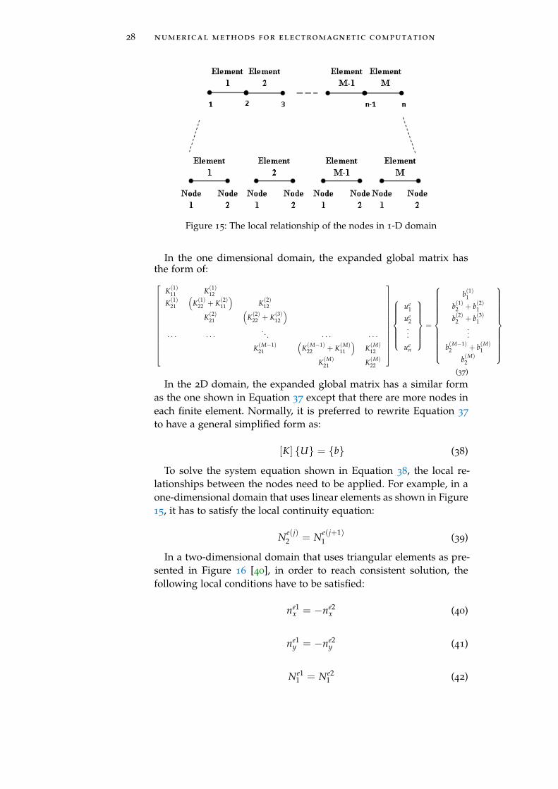
28 numerical methods for electromagnetic computation
Figure 15: The local relationship of the nodes in 1-D domain
In the one dimensional domain, the expanded global matrix hasthe form of:
K(1)11 K(1)
12
K(1)21
(K(1)
22 + K(2)11
)K(2)
12
K(2)21
(K(2)
22 + K(3)12
)· · · · · ·
. . . · · · · · ·K(M−1)
21
(K(M−1)
22 + K(M)11
)K(M)
12
K(M)21 K(M)
22
ue1
ue2...
uen
=
b(1)1
b(1)2 + b(2)1
b(2)2 + b(3)1...
b(M−1)2 + b(M)
1
b(M)2
(37)
In the 2D domain, the expanded global matrix has a similar formas the one shown in Equation 37 except that there are more nodes ineach finite element. Normally, it is preferred to rewrite Equation 37
to have a general simplified form as:
[K] U = b (38)
To solve the system equation shown in Equation 38, the local re-lationships between the nodes need to be applied. For example, in aone-dimensional domain that uses linear elements as shown in Figure15, it has to satisfy the local continuity equation:
Ne(j)2 = Ne(j+1)
1 (39)
In a two-dimensional domain that uses triangular elements as pre-sented in Figure 16 [40], in order to reach consistent solution, thefollowing local conditions have to be satisfied:
ne1x = −ne2
x (40)
ne1y = −ne2
y (41)
Ne11 = Ne2
1 (42)
2.3 finite element method 29
Figure 16: The continuous condition of the domain using triangular finiteelement
Ne12 = Ne2
3 (43)
After applying these local conditions as well as the global bound-ary conditions, the system of equation can be solved. Normally thesystem equations are required to be solved with aid of the computerprograms as it usually consists of a large amount of linear equationsfor a single frequency. The size of the global system equation is de-termined by the number of nodes and elements inside the subject do-main. This is the reason why large computation time and computermemory are required when solving an electrically large antenna us-ing the FEM technique.
2.3.2 Using FEM in 1D and 2D domain
In this section, the general solutions of several common differentialequations solved by using FEM technique will be presented. In one di-mensional domain, with the general solution the calculation is muchmore straightforward than in the two dimensional domain. Hence, inthis section, for the 2D domain problem, after introducing the generalsolution of the differential equations, two examples of using MAT-LAB to solve EM problems based on the FEM technique are given.
2.3.2.1 One-dimensional Problem using FEM
Assume the differential Equation 44 needs to be solved in one di-mensional domain and its domain has been discretized into M linearelements as shown in Figure 17.
− ddx
(α
dΦdx
)+ βΦ = f (44)

30 numerical methods for electromagnetic computation
where Φ is the unknown function, α and β are known parameters.The unknown function Φ inside each finite element can be repre-sented by using Equation 18 and can be written as:
Φe(x) =2
∑j=1
Nej (x)Φe
j (45)
Figure 17: A mesh with M linear elements in one-dimensional domain
By letting the interpolating function Ne have the general form givenby Equation 23 and apply the condition presented in Equation 26, theNe can be found to be:
Ne1(x) =
xe2 − xle (46)
Ne2(x) =
x− xe1
le (47)
where le is the length of each segment:
le = xe2 − xe
1 (48)
After applying the Galerkin’s Method, the weighted residual canbe derived to have the following form [39]:
Re = [Ke] Φe − be − ge (49)
where:
Keij =
∫ xe2
xe1
(α
dNei
dx
dNej
dx+ βNe
i Nej
)dx (50)
bei =
∫ xe2
xe1
Nei f dx (51)
gei = αNe
idΦdx|x=xe
2−αNe
idΦdx|x=xe
1(52)
Let Re = 0 can lead to the general solution of a one-dimensionalproblem that needs to solve the 1st order differential equation shown

2.3 finite element method 31
in Equation 44. Following the general rules of the FEM technique, [41]gives the general solution for the following second order differentialequation in the one-dimensional domain:
ad2udx2 + b
dudx
+ cu = f (x) (53)
where a, b, c are given constants. Using the linear shape function, [41]derived that:
Ke =∫ xi+1
xi
(−a
H′1H′2
[H′1 H′2
]+ b
H′1H′2
[H′1 H′2
]+ c
H′1H′2
[H′1 H′2
])dx
(54)
Fe = be+ ge = le
2
H1
H2
dx (55)
where:
H1(x) =xi+1 − x
le (56)
H2(x) =x− xi
le (57)
The expression of Ke can be calculated by evaluating the integra-tion with the linear interpolating function given in Equation 23. Sincein one-dimensional domain, the domain is discretized into linear seg-ment with only two nodes, so Ke can be further derived to have amore simple form as:
Ke = − ale
[1 −1
−1 1
]+
b2
[−1 1
−1 1
]+
c le
6
[2 1
1 2
](58)
Then, the global system matrix can be formed according to theEquation 37 and the solution can be found by taking into considera-tion of the global boundary conditions of the domain and the localrelationship of the nodes as presented in Equation 39.
2.3.2.2 Two-Dimensional Problem using FEM
In the two-dimensional domain, assume that the following differen-tial equation needs to be solved:
− ∂
∂x
(αx
∂Φ∂x
)− ∂
∂y
(αy
∂Φ∂y
)+ βΦ = f (59)
where Φ is the unknown function, αx, αy and β are constant, f is afunction of x and y. In two dimensional domain, the derivation of thegeneral solution is much more complicated than in one-dimensional
32 numerical methods for electromagnetic computation
domain as the increasing of nodes and unknown variables. The gen-eral solution for the equation shown in Equation 59 is given in [39].Firstly, the unknown function is approximated by using the interpo-lating functions:
Φe(x, y) =3
∑j=1
Nej (x, y)Φe
j (60)
In [39], the domain is discretized using triangular elements. Usingthe weak formulation and the general form (Equation 24) as well asthe characteristics of a interpolation function given in Equation 26
and 27, the interpolating function Ne can be found to be:
Nej (x, y) =
12∆e (ae
j + bejx + ce
jy) (61)
where:ae
1 = xe2ye
3 − ye2xe
3 (62)
be1 = ye
2 − ye3 (63)
ce1 = xe
3 − xe2 (64)
ae2 = xe
3ye1 − ye
3xe1 (65)
be2 = ye
3 − ye1 (66)
ce2 = xe
1 − xe3 (67)
ae3 = xe
1ye2 − ye
1xe2 (68)
be3 = ye
1 − ye2 (69)
ce3 = xe
2 − xe1 (70)
∆e =12
1 xe1 ye
1
1 xe2 ye
2
1 xe3 ye
3
(71)
The weighted residual can be written in the following form:
Re = [Ke] Φe − be − ge (72)
where:
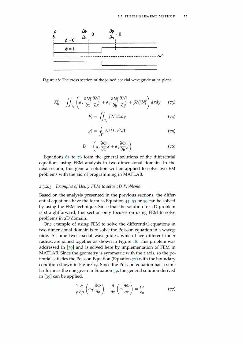
2.3 finite element method 33
Figure 18: The cross section of the joined coaxial waveguide at ρz plane
Keij =
∫∫Ωe
(αx
∂Nei
∂x
∂Nej
∂x+ αy
∂Nei
∂y
∂Nej
∂y+ βNe
i Nej
)dxdy (73)
bei =
∫∫Ωe
f Nei dxdy (74)
gei =
∮Γe
Nei D · nedΓ (75)
D =
(αx
∂Φ∂x
x + αy∂Φ∂y
y)
(76)
Equations 61 to 76 form the general solutions of the differentialequations using FEM analysis in two-dimensional domain. In thenext section, this general solution will be applied to solve two EMproblems with the aid of programming in MATLAB.
2.3.2.3 Examples of Using FEM to solve 2D Problems
Based on the analysis presented in the previous sections, the differ-ential equations have the form as Equation 44, 53 or 59 can be solvedby using the FEM technique. Since that the solution for 1D problemis straightforward, this section only focuses on using FEM to solveproblems in 2D domain.
One example of using FEM to solve the differential equations intwo dimensional domain is to solve the Poisson equation in a waveg-uide. Assume two coaxial waveguides, which have different innerradius, are joined together as shown in Figure 18. This problem wasaddressed in [39] and is solved here by implementation of FEM inMATLAB. Since the geometry is symmetric with the z axis, so the po-tential satisfies the Poisson Equation (Equation 77) with the boundarycondition shown in Figure 19. Since the Poisson equation has a simi-lar form as the one given in Equation 59, the general solution derivedin [39] can be applied.
− 1ρ
∂
∂ρ
(εrρ
∂Φ∂ρ
)− ∂
∂z
(εr
∂Φ∂z
)=
ρc
ε0(77)
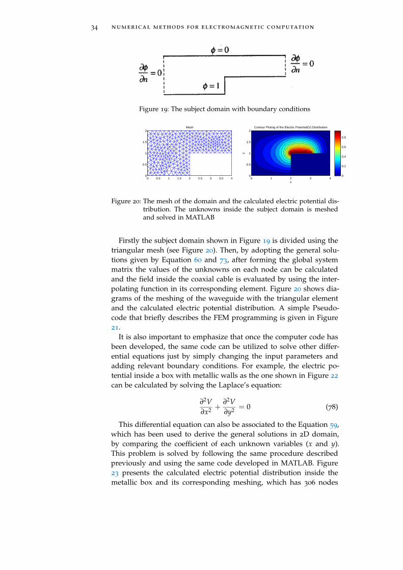
34 numerical methods for electromagnetic computation
Figure 19: The subject domain with boundary conditions
0 0.5 1 1.5 2 2.5 3 3.5 40
0.5
1
1.5
2Mesh
x
y
Contour Ploting of the Electric Potential(V) Distribution
0 1 2 3 40
0.5
1
1.5
2
0
0.2
0.4
0.6
0.8
Figure 20: The mesh of the domain and the calculated electric potential dis-tribution. The unknowns inside the subject domain is meshedand solved in MATLAB
Firstly the subject domain shown in Figure 19 is divided using thetriangular mesh (see Figure 20). Then, by adopting the general solu-tions given by Equation 60 and 73, after forming the global systemmatrix the values of the unknowns on each node can be calculatedand the field inside the coaxial cable is evaluated by using the inter-polating function in its corresponding element. Figure 20 shows dia-grams of the meshing of the waveguide with the triangular elementand the calculated electric potential distribution. A simple Pseudo-code that briefly describes the FEM programming is given in Figure21.
It is also important to emphasize that once the computer code hasbeen developed, the same code can be utilized to solve other differ-ential equations just by simply changing the input parameters andadding relevant boundary conditions. For example, the electric po-tential inside a box with metallic walls as the one shown in Figure 22
can be calculated by solving the Laplace’s equation:
∂2V∂x2 +
∂2V∂y2 = 0 (78)
This differential equation can also be associated to the Equation 59,which has been used to derive the general solutions in 2D domain,by comparing the coefficient of each unknown variables (x and y).This problem is solved by following the same procedure describedpreviously and using the same code developed in MATLAB. Figure23 presents the calculated electric potential distribution inside themetallic box and its corresponding meshing, which has 306 nodes
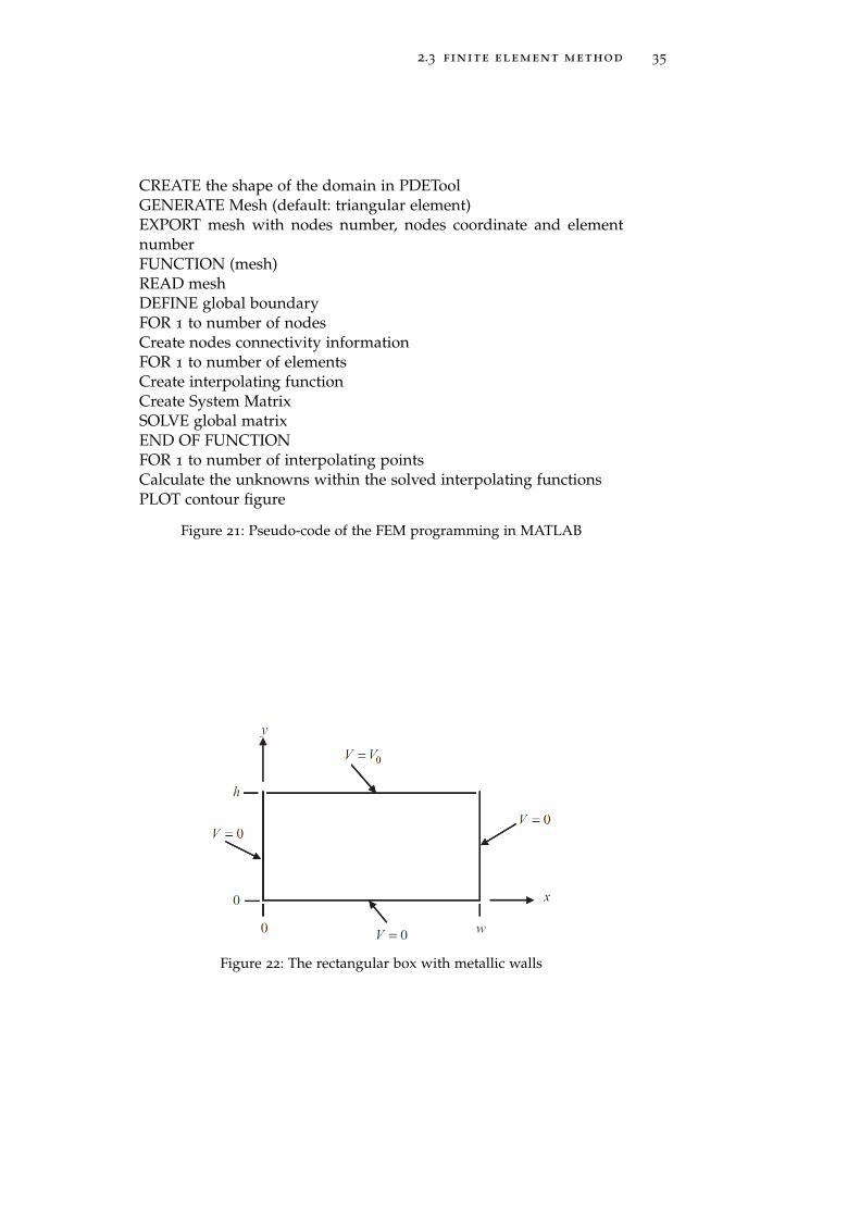
2.3 finite element method 35
CREATE the shape of the domain in PDEToolGENERATE Mesh (default: triangular element)EXPORT mesh with nodes number, nodes coordinate and elementnumberFUNCTION (mesh)READ meshDEFINE global boundaryFOR 1 to number of nodesCreate nodes connectivity informationFOR 1 to number of elementsCreate interpolating functionCreate System MatrixSOLVE global matrixEND OF FUNCTIONFOR 1 to number of interpolating pointsCalculate the unknowns within the solved interpolating functionsPLOT contour figure
Figure 21: Pseudo-code of the FEM programming in MATLAB
Figure 22: The rectangular box with metallic walls
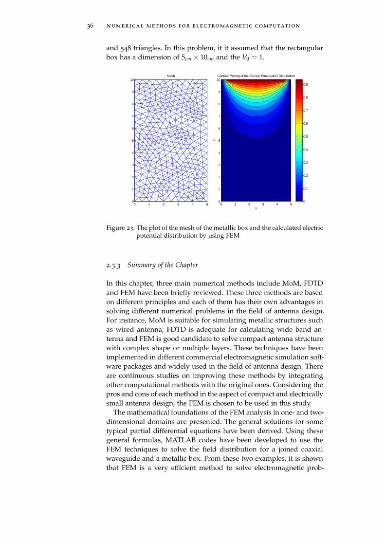
36 numerical methods for electromagnetic computation
and 548 triangles. In this problem, it it assumed that the rectangularbox has a dimension of 5cm × 10cm and the V0 = 1.
0 1 2 3 4 50
1
2
3
4
5
6
7
8
9
10Mesh
xy
Contour Ploting of the Electric Potential(V) Distribution
0 1 2 3 4 50
1
2
3
4
5
6
7
8
9
10
0
0.1
0.2
0.3
0.4
0.5
0.6
0.7
0.8
0.9
Figure 23: The plot of the mesh of the metallic box and the calculated electricpotential distribution by using FEM
2.3.3 Summary of the Chapter
In this chapter, three main numerical methods include MoM, FDTDand FEM have been briefly reviewed. These three methods are basedon different principles and each of them has their own advantages insolving different numerical problems in the field of antenna design.For instance, MoM is suitable for simulating metallic structures suchas wired antenna; FDTD is adequate for calculating wide band an-tenna and FEM is good candidate to solve compact antenna structurewith complex shape or multiple layers. These techniques have beenimplemented in different commercial electromagnetic simulation soft-ware packages and widely used in the field of antenna design. Thereare continuous studies on improving these methods by integratingother computational methods with the original ones. Considering thepros and cons of each method in the aspect of compact and electricallysmall antenna design, the FEM is chosen to be used in this study.
The mathematical foundations of the FEM analysis in one- and two-dimensional domains are presented. The general solutions for sometypical partial differential equations have been derived. Using thesegeneral formulas, MATLAB codes have been developed to use theFEM techniques to solve the field distribution for a joined coaxialwaveguide and a metallic box. From these two examples, it is shownthat FEM is a very efficient method to solve electromagnetic prob-

2.3 finite element method 37
lems that involves differential or partial differential equations. Thecomputation method, which is usually written in computer code, canalways be re-used to solve other similar problems as presented in thetwo examples.
Regarding to the use of FEM in antenna design, as the large com-plexity of the mathematical analysis due to the fact that the antennasare required to be modeled in 3D domain and it is also critical toemploy suitable model of the antenna excitation, this subject is notaddressed in this thesis work. Generally, commercial numerical sim-ulation software is required to aid the antenna design. In the rest ofthis thesis, all of the antennas are designed and simulated in AnsoftHFSS.


Part II
C O M PA C T A N T E N N A A N D A N T E N N A A R R AYD E S I G N

3F R A C TA L A N T E N N A D E S I G N
3.1 introduction
This chapter presents the design of compact printed monopole anten-nas using fractal techniques. The objective of this study is to utilizethe space filling characteristic of the fractals to reduce the size of amonopole antenna whilst maintain its good radiation performance.Moreover, it also aims to make such compact antennas operate atmultiple frequency bands of interests.
This chapter is organized as follows. Firstly the basics of fractalsand the use of mathematical methods to generate fractal geometriesare introduced in Section 3.2. Then, a methodology that utilizes MAT-LAB to aid the modeling of fractals in EM simulation tool, is demon-strated in Section 3.3. With the help of these developed MATLABfunctions, several fractal-based multiband printed monopole anten-nas have been proposed. Section 3.4 introduces two multiband frac-tal monopoles using Minkowski Island geometry. Section 3.5 and 3.6present two fractal inspired antennas for WLAN USB dongle applica-tion. One single feed fractal monopole antenna array, which exhibitshigher directivity as a result of employing two identical fractal ele-ments, is demonstrated in Section 3.7. Section 3.8 is a brief summaryof this chapter.
3.2 basics of fractal geometry
In 1975, Mandelbrot coined the word "fractal" from the Latin word’fractus’ to label objects or shapes that have similar properties at alllevels of magnification or across all times. Mandelbrot defined fractalas:
"A fractal is by definition a set for which the Hausdorff-Besicovitch dimension strictly exceeds the topological di-mension" [42].
The Hausdorff-Besicovitch dimension, which is also referred as Haus-dorff dimension in some literature, is one of the most important meth-ods to define the dimension of a fractal geometry. The dimension of afractal geometry is greater than one but smaller than two and cannotbe expressed as an integer. In this case, it is required to use the Haus-dorff dimension to describe it. For a fractal F, its Hausdorff dimensionis defined as [43]:
41
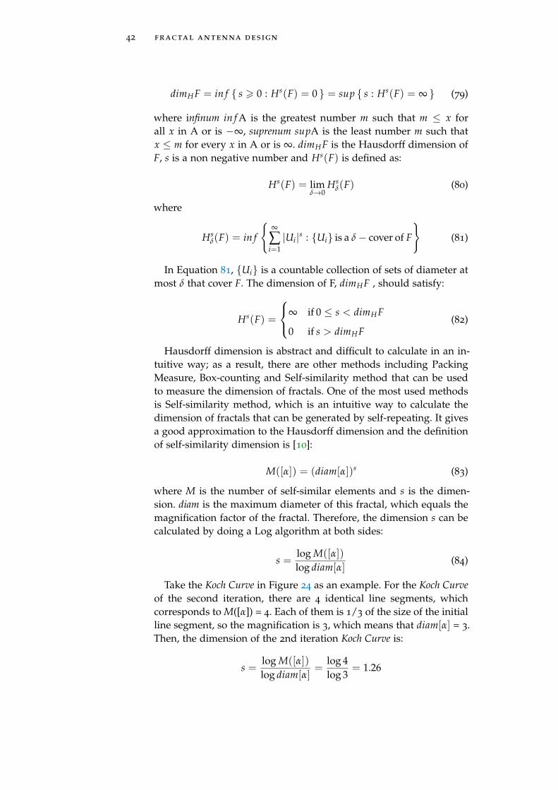
42 fractal antenna design
dimH F = in f s > 0 : Hs(F) = 0 = sup s : Hs(F) = ∞ (79)
where infinum in f A is the greatest number m such that m ≤ x forall x in A or is −∞, suprenum supA is the least number m such thatx ≤ m for every x in A or is ∞. dimH F is the Hausdorff dimension ofF, s is a non negative number and Hs(F) is defined as:
Hs(F) = limδ→0
Hsδ(F) (80)
where
Hsδ(F) = in f
∞
∑i=1|Ui|s : Ui is a δ− cover of F
(81)
In Equation 81, Ui is a countable collection of sets of diameter atmost δ that cover F. The dimension of F, dimH F , should satisfy:
Hs(F) =
∞ if 0 ≤ s < dimH F
0 if s > dimH F(82)
Hausdorff dimension is abstract and difficult to calculate in an in-tuitive way; as a result, there are other methods including PackingMeasure, Box-counting and Self-similarity method that can be usedto measure the dimension of fractals. One of the most used methodsis Self-similarity method, which is an intuitive way to calculate thedimension of fractals that can be generated by self-repeating. It givesa good approximation to the Hausdorff dimension and the definitionof self-similarity dimension is [10]:
M([α]) = (diam[α])s (83)
where M is the number of self-similar elements and s is the dimen-sion. diam is the maximum diameter of this fractal, which equals themagnification factor of the fractal. Therefore, the dimension s can becalculated by doing a Log algorithm at both sides:
s =log M([α])
log diam[α](84)
Take the Koch Curve in Figure 24 as an example. For the Koch Curveof the second iteration, there are 4 identical line segments, whichcorresponds to M([α]) = 4. Each of them is 1/3 of the size of the initialline segment, so the magnification is 3, which means that diam[α] = 3.Then, the dimension of the 2nd iteration Koch Curve is:
s =log M([α])
log diam[α]=
log 4log 3
= 1.26
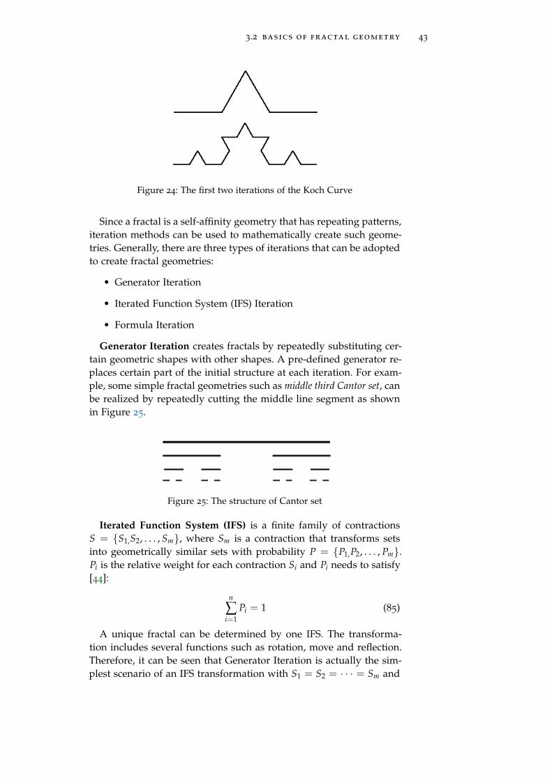
3.2 basics of fractal geometry 43
Figure 24: The first two iterations of the Koch Curve
Since a fractal is a self-affinity geometry that has repeating patterns,iteration methods can be used to mathematically create such geome-tries. Generally, there are three types of iterations that can be adoptedto create fractal geometries:
• Generator Iteration
• Iterated Function System (IFS) Iteration
• Formula Iteration
Generator Iteration creates fractals by repeatedly substituting cer-tain geometric shapes with other shapes. A pre-defined generator re-places certain part of the initial structure at each iteration. For exam-ple, some simple fractal geometries such as middle third Cantor set, canbe realized by repeatedly cutting the middle line segment as shownin Figure 25.
Figure 25: The structure of Cantor set
Iterated Function System (IFS) is a finite family of contractionsS = S1,S2, . . . , Sm, where Sm is a contraction that transforms setsinto geometrically similar sets with probability P = P1,P2, . . . , Pm.Pi is the relative weight for each contraction Si and Pi needs to satisfy[44]:
n
∑i=1
Pi = 1 (85)
A unique fractal can be determined by one IFS. The transforma-tion includes several functions such as rotation, move and reflection.Therefore, it can be seen that Generator Iteration is actually the sim-plest scenario of an IFS transformation with S1 = S2 = · · · = Sm and
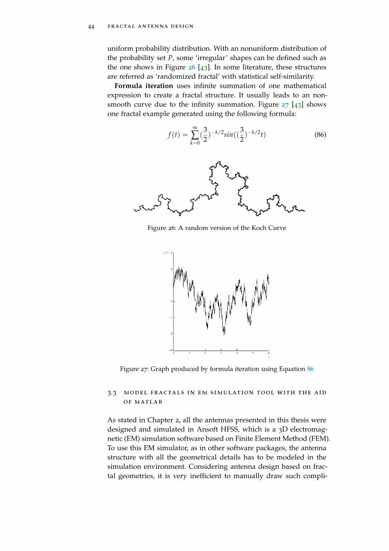
44 fractal antenna design
uniform probability distribution. With an nonuniform distribution ofthe probability set P, some ‘irregular’ shapes can be defined such asthe one shows in Figure 26 [43]. In some literature, these structuresare referred as ‘randomized fractal’ with statistical self-similarity.
Formula iteration uses infinite summation of one mathematicalexpression to create a fractal structure. It usually leads to an non-smooth curve due to the infinity summation. Figure 27 [43] showsone fractal example generated using the following formula:
f (t) =∞
∑k=0
(32)−k/2sin((
32)−k/2t) (86)
Figure 26: A random version of the Koch Curve
Figure 27: Graph produced by formula iteration using Equation 86
3.3 model fractals in em simulation tool with the aid
of matlab
As stated in Chapter 2, all the antennas presented in this thesis weredesigned and simulated in Ansoft HFSS, which is a 3D electromag-netic (EM) simulation software based on Finite Element Method (FEM).To use this EM simulator, as in other software packages, the antennastructure with all the geometrical details has to be modeled in thesimulation environment. Considering antenna design based on frac-tal geometries, it is very inefficient to manually draw such compli-
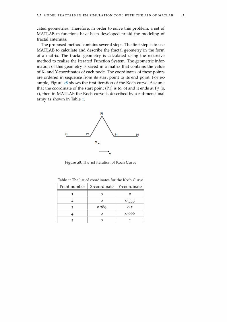
3.3 model fractals in em simulation tool with the aid of matlab 45
cated geometries. Therefore, in order to solve this problem, a set ofMATLAB m-functions have been developed to aid the modeling offractal antennas.
The proposed method contains several steps. The first step is to useMATLAB to calculate and describe the fractal geometry in the formof a matrix. The fractal geometry is calculated using the recursivemethod to realize the Iterated Function System. The geometric infor-mation of this geometry is saved in a matrix that contains the valueof X- and Y-coordinates of each node. The coordinates of these pointsare ordered in sequence from its start point to its end point. For ex-ample, Figure 28 shows the first iteration of the Koch curve. Assumethat the coordinate of the start point (P1) is (0, 0) and it ends at P5 (0,1), then in MATLAB the Koch curve is described by a 2-dimensionalarray as shown in Table 1.
Figure 28: The 1st iteration of Koch Curve
Table 1: The list of coordinates for the Koch Curve
Point number X-coordinate Y-coordinate
1 0 0
2 0 0.333
3 0.289 0.5
4 0 0.666
5 0 1
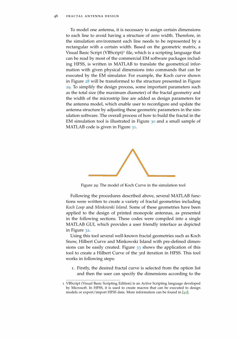
46 fractal antenna design
To model one antenna, it is necessary to assign certain dimensionsto each line to avoid having a structure of zero width. Therefore, inthe simulation environment each line needs to be represented by arectangular with a certain width. Based on the geometric matrix, aVisual Basic Script (VBScript)1 file, which is a scripting language thatcan be read by most of the commercial EM software packages includ-ing HFSS, is written in MATLAB to translate the geometrical infor-mation with given physical dimensions into commands that can beexecuted by the EM simulator. For example, the Koch curve shownin Figure 28 will be transformed to the structure presented in Figure29. To simplify the design process, some important parameters suchas the total size (the maximum diameter) of the fractal geometry andthe width of the microstrip line are added as design parameters forthe antenna model, which enable user to reconfigure and update theantenna structure by adjusting these geometric parameters in the sim-ulation software. The overall process of how to build the fractal in theEM simulation tool is illustrated in Figure 30 and a small sample ofMATLAB code is given in Figure 31.
Figure 29: The model of Koch Curve in the simulation tool
Following the procedures described above, several MATLAB func-tions were written to create a variety of fractal geometries includingKoch Loop and Minkowski Island. Some of these geometries have beenapplied to the design of printed monopole antennas, as presentedin the following sections. These codes were compiled into a singleMATLAB GUI, which provides a user friendly interface as depictedin Figure 32.
Using this tool several well-known fractal geometries such as KochSnow, Hilbert Curve and Minkowski Island with pre-defined dimen-sions can be easily created. Figure 33 shows the application of thistool to create a Hilbert Curve of the 3rd iteration in HFSS. This toolworks in following steps:
1. Firstly, the desired fractal curve is selected from the option listand then the user can specify the dimensions according to the
1 VBScript (Visual Basic Scripting Edition) is an Active Scripting language developedby Microsoft. In HFSS, it is used to create macros that can be executed to designmodels or export/import HFSS data. More information can be found in [45].
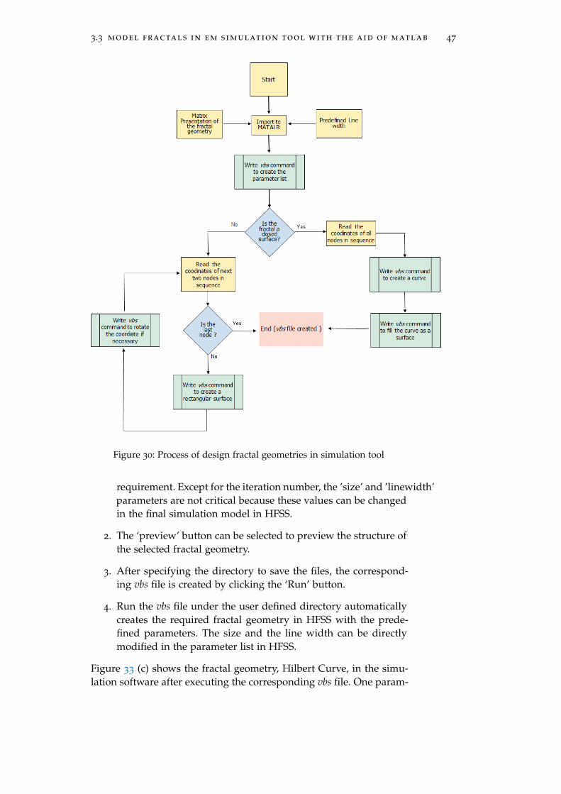
3.3 model fractals in em simulation tool with the aid of matlab 47
Figure 30: Process of design fractal geometries in simulation tool
requirement. Except for the iteration number, the ’size’ and ’linewidth’parameters are not critical because these values can be changedin the final simulation model in HFSS.
2. The ‘preview’ button can be selected to preview the structure ofthe selected fractal geometry.
3. After specifying the directory to save the files, the correspond-ing vbs file is created by clicking the ‘Run’ button.
4. Run the vbs file under the user defined directory automaticallycreates the required fractal geometry in HFSS with the prede-fined parameters. The size and the line width can be directlymodified in the parameter list in HFSS.
Figure 33 (c) shows the fractal geometry, Hilbert Curve, in the simu-lation software after executing the corresponding vbs file. One param-

48 fractal antenna design
function test_MinLoop
close all;
hfssScriptFile = ’E:\fractal design\fractal.vbs’; % set up
file path
fid = fopen(hfssScriptFile, ’wt’); % create vb file for a
new project
createNewProject(fid);
% add Local variables
addLocalVariable(fid,’size’,25); % use "size" to control
the overall length of the fractal
addLocalVariable(fid,’w’,0.25); % use "w" to control the
width of the microstrip line
iteration = 2; % define the iteration of the fractal
geometry
d = 4; % d is the depth of each iteration
fractal_curve_new(fid,iteration,d); % translate into the
final vbs file
fclose(fid); % close the vbs file
Figure 31: Example of MATLAB coding to create vbs file for designing frac-tal in HFSS
eter list, which enable one to adjust the fractal by updating the valueof each parameter, is also created as depicted in Figure 33(b).
One additional tool was also created in MATLAB, which aims tocreate a microstrip impedance transformer line. This tool adopts twotechniques, triangular taper and exponential taper, to design a mi-crostrip line with the desired impedance characteristics. With thistool, the design of an impedance matching line for printed microstripantenna is greatly simplified. Figure 34 (a) shows the interface of thistool and Figure 34 (b) presents one example of its application to cre-ate one impedance transformer line using triangular taper in HFSS.In this example, it is assumed that the substrate has permittivity of3.38 and thickness of 0.813 mm. The theoretical explanation of thetapered microstrip transmission line can be found in [46].
In following sections, several proposed fractal-based printed monopoleantennas are going to be presented. All of these antennas were de-signed by utilizing the tools described above.
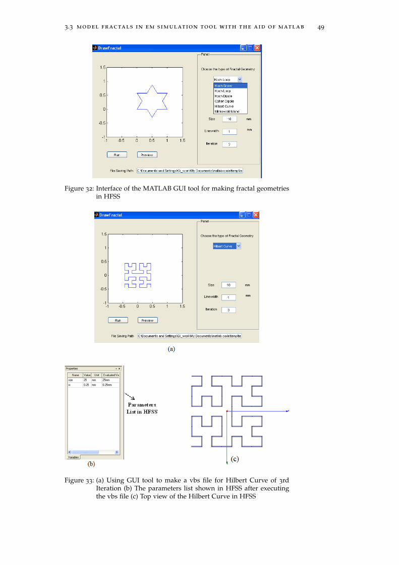
3.3 model fractals in em simulation tool with the aid of matlab 49
Figure 32: Interface of the MATLAB GUI tool for making fractal geometriesin HFSS
Figure 33: (a) Using GUI tool to make a vbs file for Hilbert Curve of 3rdIteration (b) The parameters list shown in HFSS after executingthe vbs file (c) Top view of the Hilbert Curve in HFSS

50 fractal antenna design
Figure 34: (a) Using GUI tool to make a vbs file for designing a microstripimpedance match line using the triangular taper technique; theimpedance of this microstrip line is transformed from 50 to 100
ohm (b) Top view of the designed microstrip impedance line inHFSS
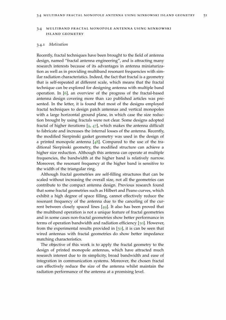
3.4 multiband fractal monopole antenna using minkowski island geometry 51
3.4 multiband fractal monopole antenna using minkowski
island geometry
3.4.1 Motivation
Recently, fractal techniques have been brought to the field of antennadesign, named “fractal antenna engineering”, and is attracting manyresearch interests because of its advantages in antenna miniaturiza-tion as well as in providing multiband resonant frequencies with sim-ilar radiation characteristics. Indeed, the fact that fractal is a geometrythat is self-repeated at different scale, which means that the fractaltechnique can be explored for designing antenna with multiple bandoperation. In [6], an overview of the progress of the fractal-basedantenna design covering more than 120 published articles was pre-sented. In the letter, it is found that most of the designs employedfractal techniques to design patch antennas and vertical monopoleswith a large horizontal ground plane, in which case the size reduc-tion brought by using fractals were not clear. Some designs adoptedfractal of higher iterations [9, 47], which makes the antenna difficultto fabricate and increases the internal losses of the antenna. Recently,the modified Sierpinski gasket geometry was used in the design ofa printed monopole antenna [48]. Compared to the use of the tra-ditional Sierpinski geometry, the modified structure can achieve ahigher size reduction. Although this antenna can operate at multiplefrequencies, the bandwidth at the higher band is relatively narrow.Moreover, the resonant frequency at the higher band is sensitive tothe width of the triangular ring.
Although fractal geometries are self-filling structures that can bescaled without increasing the overall size, not all the geometries cancontribute to the compact antenna design. Previous research foundthat some fractal geometries such as Hilbert and Peano curves, whichexhibit a high degree of space filling, cannot effectively reduce theresonant frequency of the antenna due to the canceling of the cur-rent between closely spaced lines [49]. It also has been proved thatthe multiband operation is not a unique feature of fractal geometriesand in some cases non-fractal geometries show better performance interms of operation bandwidth and radiation efficiency [50]. However,from the experimental results provided in [50], it is can be seen thatwired antennas with fractal geometries do show better impedancematching characteristics.
The objective of this work is to apply the fractal geometry to thedesign of printed monopole antennas, which have attracted muchresearch interest due to its simplicity, broad bandwidth and ease ofintegration in communication systems. Moreover, the chosen fractalcan effectively reduce the size of the antenna whilst maintain theradiation performance of the antenna at a promising level.
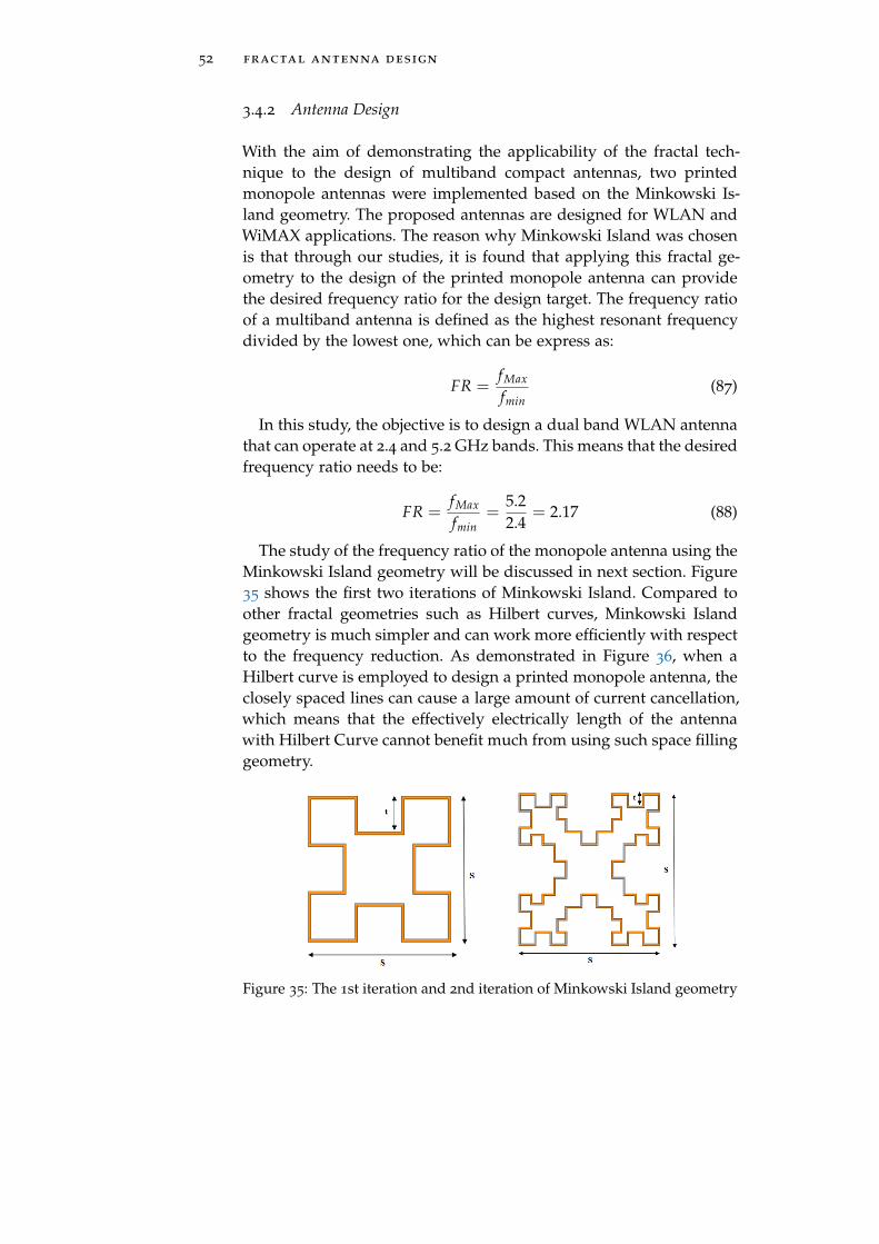
52 fractal antenna design
3.4.2 Antenna Design
With the aim of demonstrating the applicability of the fractal tech-nique to the design of multiband compact antennas, two printedmonopole antennas were implemented based on the Minkowski Is-land geometry. The proposed antennas are designed for WLAN andWiMAX applications. The reason why Minkowski Island was chosenis that through our studies, it is found that applying this fractal ge-ometry to the design of the printed monopole antenna can providethe desired frequency ratio for the design target. The frequency ratioof a multiband antenna is defined as the highest resonant frequencydivided by the lowest one, which can be express as:
FR =fMax
fmin(87)
In this study, the objective is to design a dual band WLAN antennathat can operate at 2.4 and 5.2 GHz bands. This means that the desiredfrequency ratio needs to be:
FR =fMax
fmin=
5.22.4
= 2.17 (88)
The study of the frequency ratio of the monopole antenna using theMinkowski Island geometry will be discussed in next section. Figure35 shows the first two iterations of Minkowski Island. Compared toother fractal geometries such as Hilbert curves, Minkowski Islandgeometry is much simpler and can work more efficiently with respectto the frequency reduction. As demonstrated in Figure 36, when aHilbert curve is employed to design a printed monopole antenna, theclosely spaced lines can cause a large amount of current cancellation,which means that the effectively electrically length of the antennawith Hilbert Curve cannot benefit much from using such space fillinggeometry.
Figure 35: The 1st iteration and 2nd iteration of Minkowski Island geometry
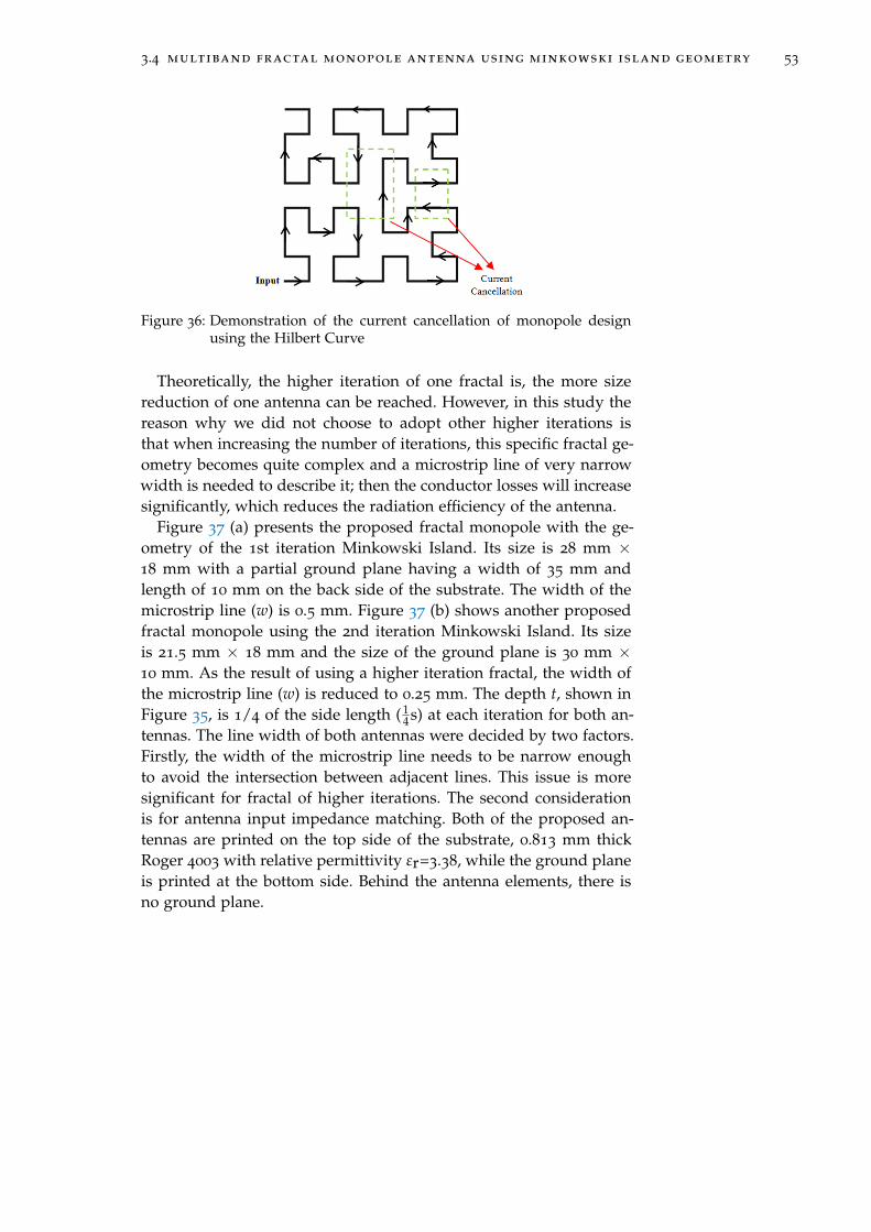
3.4 multiband fractal monopole antenna using minkowski island geometry 53
Figure 36: Demonstration of the current cancellation of monopole designusing the Hilbert Curve
Theoretically, the higher iteration of one fractal is, the more sizereduction of one antenna can be reached. However, in this study thereason why we did not choose to adopt other higher iterations isthat when increasing the number of iterations, this specific fractal ge-ometry becomes quite complex and a microstrip line of very narrowwidth is needed to describe it; then the conductor losses will increasesignificantly, which reduces the radiation efficiency of the antenna.
Figure 37 (a) presents the proposed fractal monopole with the ge-ometry of the 1st iteration Minkowski Island. Its size is 28 mm ×18 mm with a partial ground plane having a width of 35 mm andlength of 10 mm on the back side of the substrate. The width of themicrostrip line (w) is 0.5 mm. Figure 37 (b) shows another proposedfractal monopole using the 2nd iteration Minkowski Island. Its sizeis 21.5 mm × 18 mm and the size of the ground plane is 30 mm ×10 mm. As the result of using a higher iteration fractal, the width ofthe microstrip line (w) is reduced to 0.25 mm. The depth t, shown inFigure 35, is 1/4 of the side length ( 1
4 s) at each iteration for both an-tennas. The line width of both antennas were decided by two factors.Firstly, the width of the microstrip line needs to be narrow enoughto avoid the intersection between adjacent lines. This issue is moresignificant for fractal of higher iterations. The second considerationis for antenna input impedance matching. Both of the proposed an-tennas are printed on the top side of the substrate, 0.813 mm thickRoger 4003 with relative permittivity εr=3.38, while the ground planeis printed at the bottom side. Behind the antenna elements, there isno ground plane.
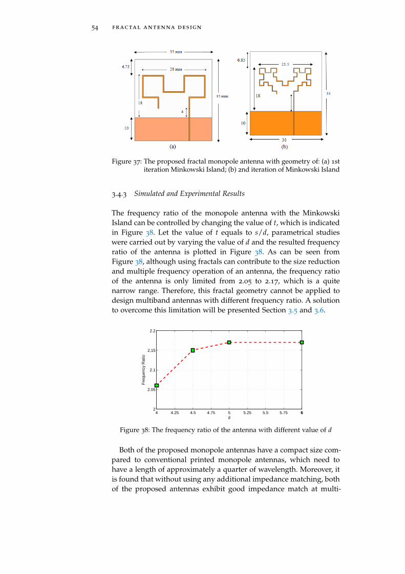
54 fractal antenna design
Figure 37: The proposed fractal monopole antenna with geometry of: (a) 1stiteration Minkowski Island; (b) 2nd iteration of Minkowski Island
3.4.3 Simulated and Experimental Results
The frequency ratio of the monopole antenna with the MinkowskiIsland can be controlled by changing the value of t, which is indicatedin Figure 38. Let the value of t equals to s/d, parametrical studieswere carried out by varying the value of d and the resulted frequencyratio of the antenna is plotted in Figure 38. As can be seen fromFigure 38, although using fractals can contribute to the size reductionand multiple frequency operation of an antenna, the frequency ratioof the antenna is only limited from 2.05 to 2.17, which is a quitenarrow range. Therefore, this fractal geometry cannot be applied todesign multiband antennas with different frequency ratio. A solutionto overcome this limitation will be presented Section 3.5 and 3.6.
4 4.25 4.5 4.75 5 5.25 5.5 5.75 662
2.05
2.1
2.15
2.2
d
Fre
quen
cy R
atio
Figure 38: The frequency ratio of the antenna with different value of d
Both of the proposed monopole antennas have a compact size com-pared to conventional printed monopole antennas, which need tohave a length of approximately a quarter of wavelength. Moreover, itis found that without using any additional impedance matching, bothof the proposed antennas exhibit good impedance match at multi-
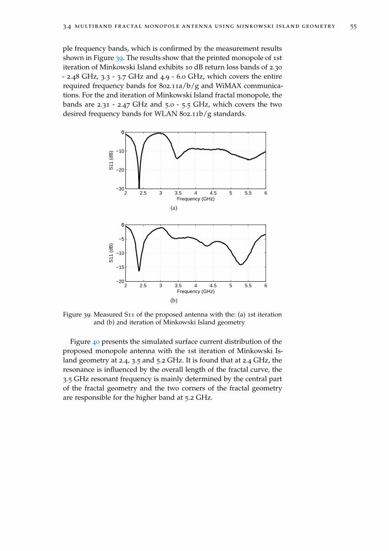
3.4 multiband fractal monopole antenna using minkowski island geometry 55
ple frequency bands, which is confirmed by the measurement resultsshown in Figure 39. The results show that the printed monopole of 1stiteration of Minkowski Island exhibits 10 dB return loss bands of 2.30
- 2.48 GHz, 3.3 - 3.7 GHz and 4.9 - 6.0 GHz, which covers the entirerequired frequency bands for 802.11a/b/g and WiMAX communica-tions. For the 2nd iteration of Minkowski Island fractal monopole, thebands are 2.31 - 2.47 GHz and 5.0 - 5.5 GHz, which covers the twodesired frequency bands for WLAN 802.11b/g standards.
2 2.5 3 3.5 4 4.5 5 5.5 6−30
−20
−10
00
Frequency (GHz)
S11
(dB
)
(a)
2 2.5 3 3.5 4 4.5 5 5.5 6−20
−15
−10
−5
00
Frequency (GHz)
S11
(dB
)
(b)
Figure 39: Measured S11 of the proposed antenna with the: (a) 1st iterationand (b) 2nd iteration of Minkowski Island geometry
Figure 40 presents the simulated surface current distribution of theproposed monopole antenna with the 1st iteration of Minkowski Is-land geometry at 2.4, 3.5 and 5.2 GHz. It is found that at 2.4 GHz, theresonance is influenced by the overall length of the fractal curve, the3.5 GHz resonant frequency is mainly determined by the central partof the fractal geometry and the two corners of the fractal geometryare responsible for the higher band at 5.2 GHz.
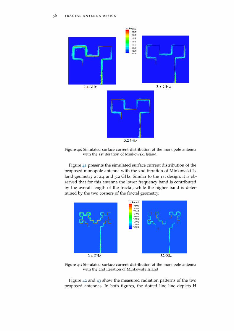
56 fractal antenna design
Figure 40: Simulated surface current distribution of the monopole antennawith the 1st iteration of Minkowski Island
Figure 41 presents the simulated surface current distribution of theproposed monopole antenna with the 2nd iteration of Minkowski Is-land geometry at 2.4 and 5.2 GHz. Similar to the 1st design, it is ob-served that for this antenna the lower frequency band is contributedby the overall length of the fractal, while the higher band is deter-mined by the two corners of the fractal geometry.
Figure 41: Simulated surface current distribution of the monopole antennawith the 2nd iteration of Minkowski Island
Figure 42 and 43 show the measured radiation patterns of the twoproposed antennas. In both figures, the dotted line line depicts H
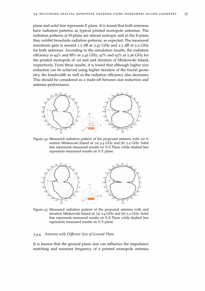
3.4 multiband fractal monopole antenna using minkowski island geometry 57
plane and solid line represents E plane. It is found that both antennashave radiation patterns as typical printed monopole antennas. Theradiation patterns at H-plane are almost isotropic and in the E-planethey exhibit broadside radiation patterns, as expected. The measuredmaximum gain is around 1.5 dB at 2.45 GHz and 2.3 dB at 5.2 GHzfor both antennas. According to the simulation results, the radiationefficiency is 94% and 88% at 2.45 GHz, 97% and 93% at 5.26 GHz forthe printed monopole of 1st and 2nd iteration of Minkowski Island,respectively. From these results, it is found that although higher sizereduction can be achieved using higher iteration of the fractal geom-etry, the bandwidth as well as the radiation efficiency also decreases.This should be considered as a trade-off between size reduction andantenna performance.
0°
15°
30°
45°
60°
75°90°105 °
120 °
135 °
150 °
165 °
±180 °
−165°
−150°
−135°
−120°
−105° −90° −75°
−60°
−45°
−30°
−15°
−16−12−8−40
(a)
0°
15°
30°
45°
60°
75°90°105 °
120 °
135 °
150 °
165 °
±180 °
−165°
−150°
−135°
−120°
−105° −90° −75°
−60°
−45°
−30°
−15°
−20−15−10−50
(b)
Figure 42: Measured radiation pattern of the proposed antenna with 1st it-eration Minkowski Island at: (a) 2.4 GHz and (b) 5.2 GHz. Solidline represents measured results on X-Z Plane while dashed linerepresents measured results on X-Y plane
0°
15°
30°
45°
60°
75°90°105 °
120 °
135 °
150 °
165 °
±180 °
−165°
−150°
−135°
−120°
−105° −90° −75°
−60°
−45°
−30°
−15°
−16−12−8−40
(a)
0°
15°
30°
45°
60°
75°90°105 °
120 °
135 °
150 °
165 °
±180 °
−165°
−150°
−135°
−120°
−105° −90° −75°
−60°
−45°
−30°
−15°
−30−20−100
(b)
Figure 43: Measured radiation pattern of the proposed antenna with 2nditeration Minkowski Island at: (a) 2.4 GHz and (b) 5.2 GHz. Solidline represents measured results on X-Z Plane while dashed linerepresents measured results on X-Y plane
3.4.4 Antenna with Different Size of Ground Plane
It is known that the ground plane size can influence the impedancematching and resonant frequency of a printed monopole antenna.
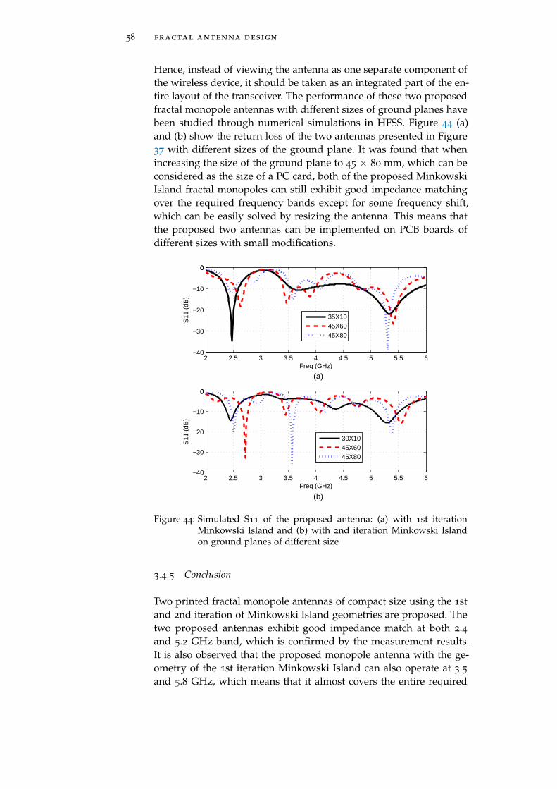
58 fractal antenna design
Hence, instead of viewing the antenna as one separate component ofthe wireless device, it should be taken as an integrated part of the en-tire layout of the transceiver. The performance of these two proposedfractal monopole antennas with different sizes of ground planes havebeen studied through numerical simulations in HFSS. Figure 44 (a)and (b) show the return loss of the two antennas presented in Figure37 with different sizes of the ground plane. It was found that whenincreasing the size of the ground plane to 45 × 80 mm, which can beconsidered as the size of a PC card, both of the proposed MinkowskiIsland fractal monopoles can still exhibit good impedance matchingover the required frequency bands except for some frequency shift,which can be easily solved by resizing the antenna. This means thatthe proposed two antennas can be implemented on PCB boards ofdifferent sizes with small modifications.
2 2.5 3 3.5 4 4.5 5 5.5 6−40
−30
−20
−10
00
Freq (GHz)
S11
(dB
)
35X1045X6045X80
(a)
2 2.5 3 3.5 4 4.5 5 5.5 6−40
−30
−20
−10
00
Freq (GHz)
S11
(dB
)
30X1045X6045X80
(b)
Figure 44: Simulated S11 of the proposed antenna: (a) with 1st iterationMinkowski Island and (b) with 2nd iteration Minkowski Islandon ground planes of different size
3.4.5 Conclusion
Two printed fractal monopole antennas of compact size using the 1stand 2nd iteration of Minkowski Island geometries are proposed. Thetwo proposed antennas exhibit good impedance match at both 2.4and 5.2 GHz band, which is confirmed by the measurement results.It is also observed that the proposed monopole antenna with the ge-ometry of the 1st iteration Minkowski Island can also operate at 3.5and 5.8 GHz, which means that it almost covers the entire required
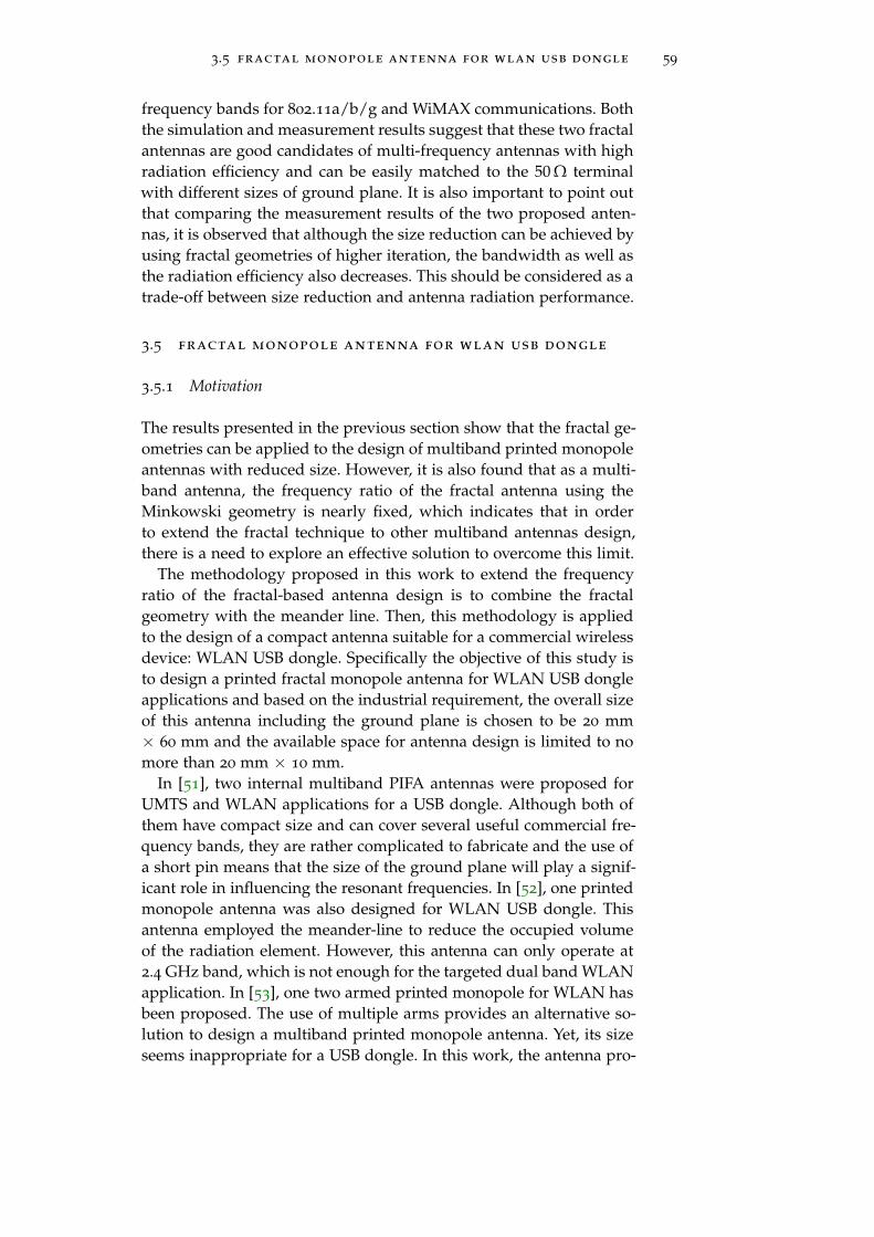
3.5 fractal monopole antenna for wlan usb dongle 59
frequency bands for 802.11a/b/g and WiMAX communications. Boththe simulation and measurement results suggest that these two fractalantennas are good candidates of multi-frequency antennas with highradiation efficiency and can be easily matched to the 50 Ω terminalwith different sizes of ground plane. It is also important to point outthat comparing the measurement results of the two proposed anten-nas, it is observed that although the size reduction can be achieved byusing fractal geometries of higher iteration, the bandwidth as well asthe radiation efficiency also decreases. This should be considered as atrade-off between size reduction and antenna radiation performance.
3.5 fractal monopole antenna for wlan usb dongle
3.5.1 Motivation
The results presented in the previous section show that the fractal ge-ometries can be applied to the design of multiband printed monopoleantennas with reduced size. However, it is also found that as a multi-band antenna, the frequency ratio of the fractal antenna using theMinkowski geometry is nearly fixed, which indicates that in orderto extend the fractal technique to other multiband antennas design,there is a need to explore an effective solution to overcome this limit.
The methodology proposed in this work to extend the frequencyratio of the fractal-based antenna design is to combine the fractalgeometry with the meander line. Then, this methodology is appliedto the design of a compact antenna suitable for a commercial wirelessdevice: WLAN USB dongle. Specifically the objective of this study isto design a printed fractal monopole antenna for WLAN USB dongleapplications and based on the industrial requirement, the overall sizeof this antenna including the ground plane is chosen to be 20 mm× 60 mm and the available space for antenna design is limited to nomore than 20 mm × 10 mm.
In [51], two internal multiband PIFA antennas were proposed forUMTS and WLAN applications for a USB dongle. Although both ofthem have compact size and can cover several useful commercial fre-quency bands, they are rather complicated to fabricate and the use ofa short pin means that the size of the ground plane will play a signif-icant role in influencing the resonant frequencies. In [52], one printedmonopole antenna was also designed for WLAN USB dongle. Thisantenna employed the meander-line to reduce the occupied volumeof the radiation element. However, this antenna can only operate at2.4 GHz band, which is not enough for the targeted dual band WLANapplication. In [53], one two armed printed monopole for WLAN hasbeen proposed. The use of multiple arms provides an alternative so-lution to design a multiband printed monopole antenna. Yet, its sizeseems inappropriate for a USB dongle. In this work, the antenna pro-
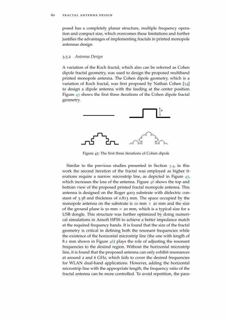
60 fractal antenna design
posed has a completely planar structure, multiple frequency opera-tion and compact size, which overcomes these limitations and furtherjustifies the advantages of implementing fractals in printed monopoleantennas design.
3.5.2 Antenna Design
A variation of the Koch fractal, which also can be referred as Cohendipole fractal geometry, was used to design the proposed multibandprinted monopole antenna. The Cohen dipole geometry, which is avariation of Koch fractal, was first proposed by Nathan Cohen [54]to design a dipole antenna with the feeding at the center position.Figure 45 shows the first three iterations of the Cohen dipole fractalgeometry.
Figure 45: The first three iterations of Cohen dipole
Similar to the previous studies presented in Section 3.4, in thiswork the second iteration of the fractal was employed as higher it-erations require a narrow microstrip line, as depicted in Figure 45,which increases the loss of the antenna. Figure 46 shows the top andbottom view of the proposed printed fractal monopole antenna. Thisantenna is designed on the Roger 4003 substrate with dielectric con-stant of 3.38 and thickness of 0.813 mm. The space occupied by themonopole antenna on the substrate is 10 mm × 20 mm and the sizeof the ground plane is 50 mm × 20 mm, which is a typical size for aUSB dongle. This structure was further optimized by doing numeri-cal simulations in Ansoft HFSS to achieve a better impedance matchat the required frequency bands. It is found that the size of the fractalgeometry is critical in defining both the resonant frequencies whilethe existence of the horizontal microstrip line (the one with length of8.1 mm shown in Figure 46) plays the role of adjusting the resonantfrequencies to the desired region. Without the horizontal microstripline, it is found that the proposed antenna can only exhibit resonancesat around 2 and 6 GHz, which fails to cover the desired frequenciesfor WLAN dual-band applications. However, adding the horizontalmicrostrip line with the appropriate length, the frequency ratio of thefractal antenna can be more controlled. To avoid repetition, the para-
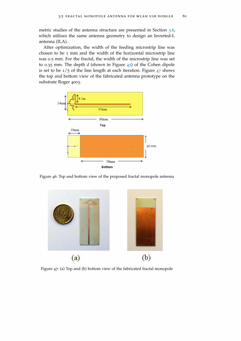
3.5 fractal monopole antenna for wlan usb dongle 61
metric studies of the antenna structure are presented in Section 3.6,which utilizes the same antenna geometry to design an Inverted-Lantenna (ILA).
After optimization, the width of the feeding microstrip line waschosen to be 1 mm and the width of the horizontal microstrip linewas 0.5 mm. For the fractal, the width of the microstrip line was setto 0.35 mm. The depth d (shown in Figure 45) of the Cohen dipoleis set to be 1/5 of the line length at each iteration. Figure 47 showsthe top and bottom view of the fabricated antenna prototype on thesubstrate Roger 4003.
Figure 46: Top and bottom view of the proposed fractal monopole antenna
Figure 47: (a) Top and (b) bottom view of the fabricated fractal monopole
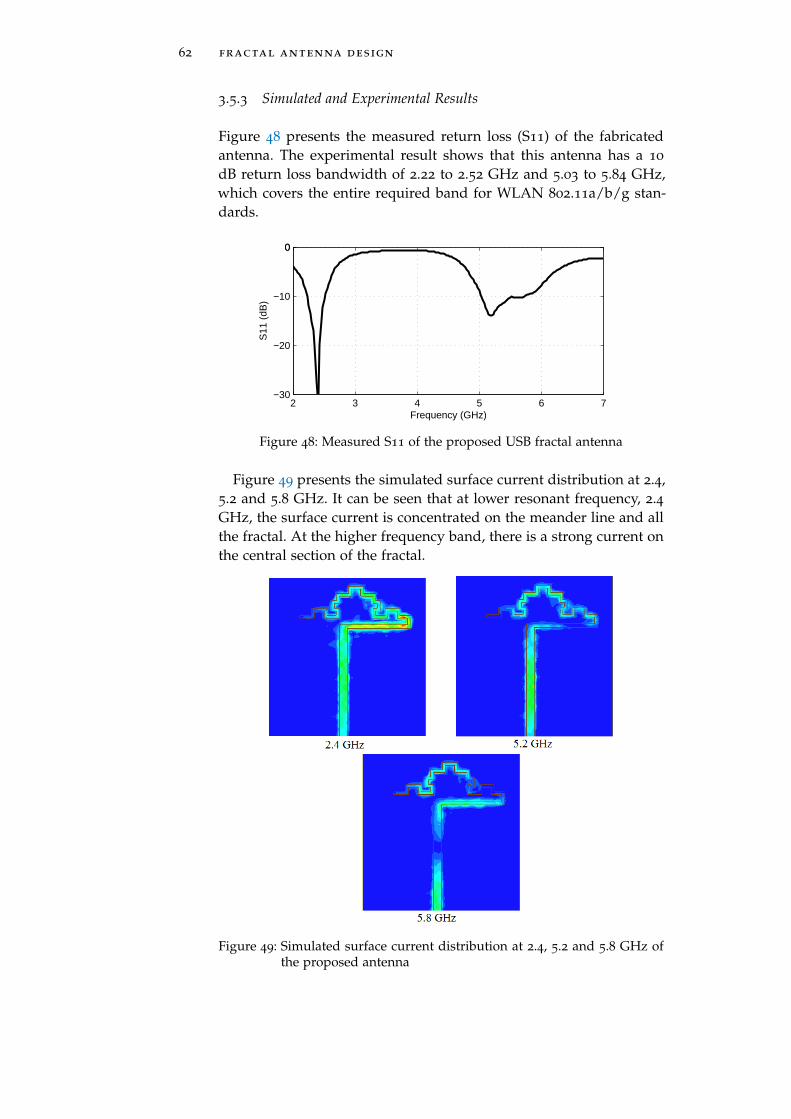
62 fractal antenna design
3.5.3 Simulated and Experimental Results
Figure 48 presents the measured return loss (S11) of the fabricatedantenna. The experimental result shows that this antenna has a 10
dB return loss bandwidth of 2.22 to 2.52 GHz and 5.03 to 5.84 GHz,which covers the entire required band for WLAN 802.11a/b/g stan-dards.
2 3 4 5 6 7−30
−20
−10
00
Frequency (GHz)
S11
(dB
)
Figure 48: Measured S11 of the proposed USB fractal antenna
Figure 49 presents the simulated surface current distribution at 2.4,5.2 and 5.8 GHz. It can be seen that at lower resonant frequency, 2.4GHz, the surface current is concentrated on the meander line and allthe fractal. At the higher frequency band, there is a strong current onthe central section of the fractal.
Figure 49: Simulated surface current distribution at 2.4, 5.2 and 5.8 GHz ofthe proposed antenna
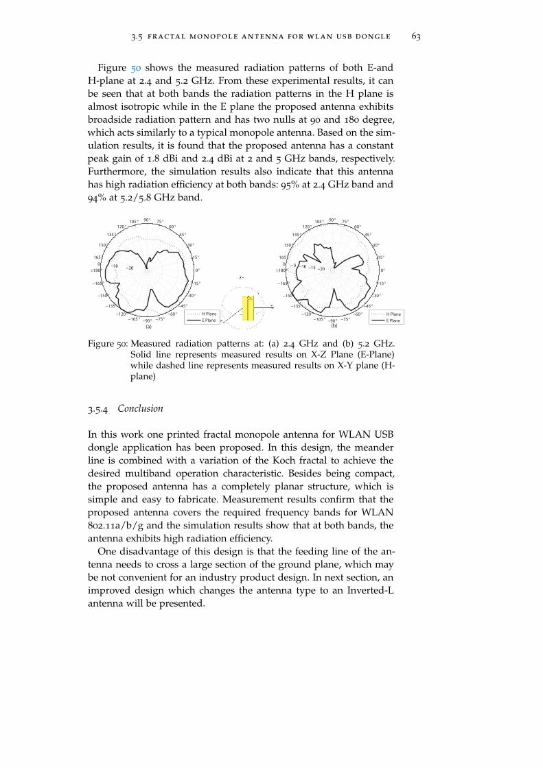
3.5 fractal monopole antenna for wlan usb dongle 63
Figure 50 shows the measured radiation patterns of both E-andH-plane at 2.4 and 5.2 GHz. From these experimental results, it canbe seen that at both bands the radiation patterns in the H plane isalmost isotropic while in the E plane the proposed antenna exhibitsbroadside radiation pattern and has two nulls at 90 and 180 degree,which acts similarly to a typical monopole antenna. Based on the sim-ulation results, it is found that the proposed antenna has a constantpeak gain of 1.8 dBi and 2.4 dBi at 2 and 5 GHz bands, respectively.Furthermore, the simulation results also indicate that this antennahas high radiation efficiency at both bands: 95% at 2.4 GHz band and94% at 5.2/5.8 GHz band.
0°
15°
30°
45°
60°
75°90°105 °
120 °
135 °
150 °
165 °
±180 °
−165°
−150°
−135°
−120°
−105° −90° −75°
−60°
−45°
−30°
−15°
−20−10
0
H Plane
E Plane
(a)
0°
15°
30°
45°
60°
75°90°105 °
120 °
135 °
150 °
165 °
±180 °
−165°
−150°
−135°
−120°
−105° −90° −75°
−60°
−45°
−30°
−15°
−20−15−10−50
H Plane
E Plane
(b)
Figure 50: Measured radiation patterns at: (a) 2.4 GHz and (b) 5.2 GHz.Solid line represents measured results on X-Z Plane (E-Plane)while dashed line represents measured results on X-Y plane (H-plane)
3.5.4 Conclusion
In this work one printed fractal monopole antenna for WLAN USBdongle application has been proposed. In this design, the meanderline is combined with a variation of the Koch fractal to achieve thedesired multiband operation characteristic. Besides being compact,the proposed antenna has a completely planar structure, which issimple and easy to fabricate. Measurement results confirm that theproposed antenna covers the required frequency bands for WLAN802.11a/b/g and the simulation results show that at both bands, theantenna exhibits high radiation efficiency.
One disadvantage of this design is that the feeding line of the an-tenna needs to cross a large section of the ground plane, which maybe not convenient for an industry product design. In next section, animproved design which changes the antenna type to an Inverted-Lantenna will be presented.
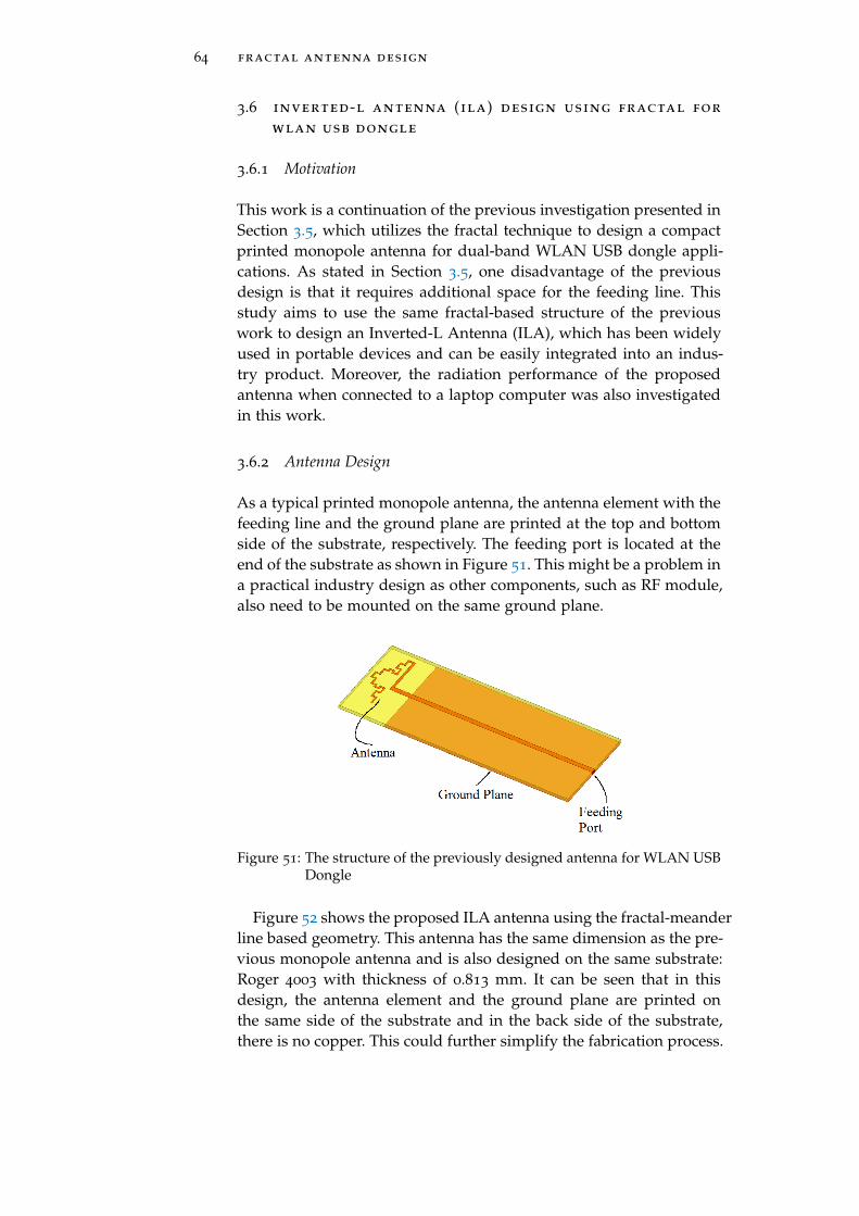
64 fractal antenna design
3.6 inverted-l antenna (ila) design using fractal for
wlan usb dongle
3.6.1 Motivation
This work is a continuation of the previous investigation presented inSection 3.5, which utilizes the fractal technique to design a compactprinted monopole antenna for dual-band WLAN USB dongle appli-cations. As stated in Section 3.5, one disadvantage of the previousdesign is that it requires additional space for the feeding line. Thisstudy aims to use the same fractal-based structure of the previouswork to design an Inverted-L Antenna (ILA), which has been widelyused in portable devices and can be easily integrated into an indus-try product. Moreover, the radiation performance of the proposedantenna when connected to a laptop computer was also investigatedin this work.
3.6.2 Antenna Design
As a typical printed monopole antenna, the antenna element with thefeeding line and the ground plane are printed at the top and bottomside of the substrate, respectively. The feeding port is located at theend of the substrate as shown in Figure 51. This might be a problem ina practical industry design as other components, such as RF module,also need to be mounted on the same ground plane.
Figure 51: The structure of the previously designed antenna for WLAN USBDongle
Figure 52 shows the proposed ILA antenna using the fractal-meanderline based geometry. This antenna has the same dimension as the pre-vious monopole antenna and is also designed on the same substrate:Roger 4003 with thickness of 0.813 mm. It can be seen that in thisdesign, the antenna element and the ground plane are printed onthe same side of the substrate and in the back side of the substrate,there is no copper. This could further simplify the fabrication process.
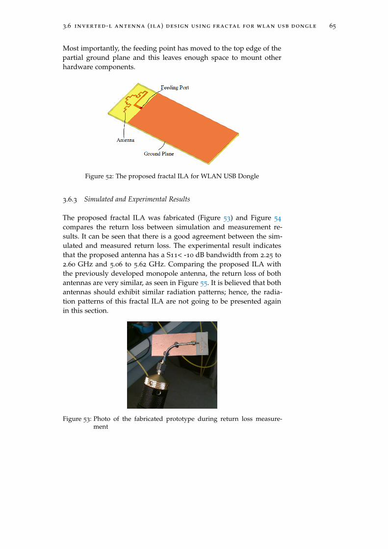
3.6 inverted-l antenna (ila) design using fractal for wlan usb dongle 65
Most importantly, the feeding point has moved to the top edge of thepartial ground plane and this leaves enough space to mount otherhardware components.
Figure 52: The proposed fractal ILA for WLAN USB Dongle
3.6.3 Simulated and Experimental Results
The proposed fractal ILA was fabricated (Figure 53) and Figure 54
compares the return loss between simulation and measurement re-sults. It can be seen that there is a good agreement between the sim-ulated and measured return loss. The experimental result indicatesthat the proposed antenna has a S11< -10 dB bandwidth from 2.25 to2.60 GHz and 5.06 to 5.62 GHz. Comparing the proposed ILA withthe previously developed monopole antenna, the return loss of bothantennas are very similar, as seen in Figure 55. It is believed that bothantennas should exhibit similar radiation patterns; hence, the radia-tion patterns of this fractal ILA are not going to be presented againin this section.
Figure 53: Photo of the fabricated prototype during return loss measure-ment
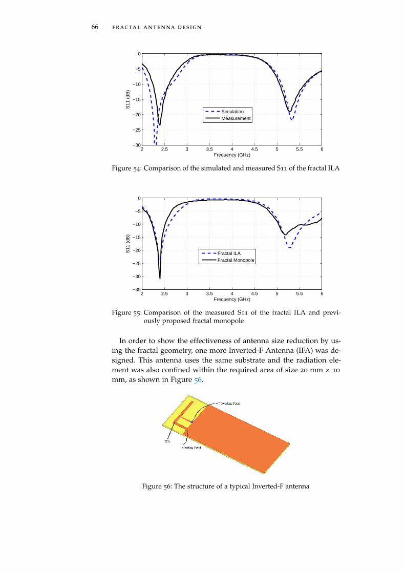
66 fractal antenna design
2 2.5 3 3.5 4 4.5 5 5.5 6−30
−25
−20
−15
−10
−5
0
Frequency (GHz)
S11
(dB
)
SimulationMeasurement
Figure 54: Comparison of the simulated and measured S11 of the fractal ILA
2 2.5 3 3.5 4 4.5 5 5.5 6−35
−30
−25
−20
−15
−10
−5
0
Frequency (GHz)
S11
(dB
)
Fractal ILAFractal Monopole
Figure 55: Comparison of the measured S11 of the fractal ILA and previ-ously proposed fractal monopole
In order to show the effectiveness of antenna size reduction by us-ing the fractal geometry, one more Inverted-F Antenna (IFA) was de-signed. This antenna uses the same substrate and the radiation ele-ment was also confined within the required area of size 20 mm × 10
mm, as shown in Figure 56.
Figure 56: The structure of a typical Inverted-F antenna
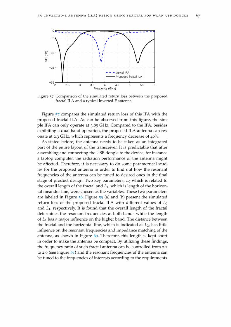
3.6 inverted-l antenna (ila) design using fractal for wlan usb dongle 67
2 2.5 3 3.5 4 4.5 5 5.5 6−35
−25
−15
−5
00
Frequency (GHz)
S11
(dB
)
typical IFAProposed fractal ILA
Figure 57: Comparison of the simulated return loss between the proposedfractal ILA and a typical Inverted-F antenna
Figure 57 compares the simulated return loss of this IFA with theproposed fractal ILA. As can be observed from this figure, the sim-ple IFA can only operate at 3.85 GHz. Compared to the IFA, besidesexhibiting a dual band operation, the proposed ILA antenna can res-onate at 2.3 GHz, which represents a frequency decrease of 40%.
As stated before, the antenna needs to be taken as an integratedpart of the entire layout of the transceiver. It is predictable that afterassembling and connecting the USB dongle to the device, for instancea laptop computer, the radiation performance of the antenna mightbe affected. Therefore, it is necessary to do some parametrical stud-ies for the proposed antenna in order to find out how the resonantfrequencies of the antenna can be tuned to desired ones in the finalstage of product design. Two key parameters, L0 which is related tothe overall length of the fractal and L1, which is length of the horizon-tal meander line, were chosen as the variables. These two parametersare labeled in Figure 58. Figure 59 (a) and (b) present the simulatedreturn loss of the proposed fractal ILA with different values of L0
and L1, respectively. It is found that the overall length of the fractaldetermines the resonant frequencies at both bands while the lengthof L1 has a major influence on the higher band. The distance betweenthe fractal and the horizontal line, which is indicated as L2, has littleinfluence on the resonant frequencies and impedance matching of theantenna, as shown in Figure 60. Therefore, this length is kept shortin order to make the antenna be compact. By utilizing these findings,the frequency ratio of such fractal antenna can be controlled from 2.2to 2.6 (see Figure 61) and the resonant frequencies of the antenna canbe tuned to the frequencies of interests according to the requirements.
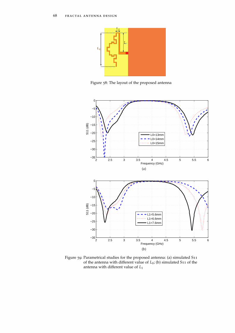
68 fractal antenna design
Figure 58: The layout of the proposed antenna
2 2.5 3 3.5 4 4.5 5 5.5 6−35
−30
−25
−20
−15
−10
−5
0
Frequency (GHz)
S11
(dB
)
L0=13mmL0=14mmL0=15mm
(a)
2 2.5 3 3.5 4 4.5 5 5.5 6−35
−30
−25
−20
−15
−10
−5
0
Frequency (GHz)
S11
(dB
)
L1=5.6mmL1=6.6mmL1=7.6mm
(b)
Figure 59: Parametrical studies for the proposed antenna: (a) simulated S11
of the antenna with different value of L0; (b) simulated S11 of theantenna with different value of L1
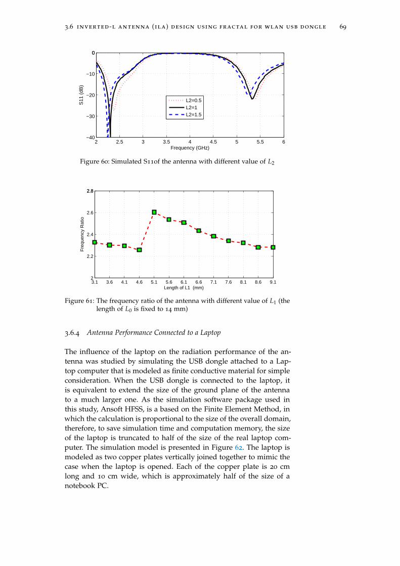
3.6 inverted-l antenna (ila) design using fractal for wlan usb dongle 69
2 2.5 3 3.5 4 4.5 5 5.5 6−40
−30
−20
−10
00
Frequency (GHz)
S11
(dB
)
L2=0.5L2=1L2=1.5
Figure 60: Simulated S11of the antenna with different value of L2
3.1 3.6 4.1 4.6 5.1 5.6 6.1 6.6 7.1 7.6 8.1 8.6 9.12
2.2
2.4
2.6
2.82.8
Length of L1 (mm)
Fre
quen
cy R
atio
Figure 61: The frequency ratio of the antenna with different value of L1 (thelength of L0 is fixed to 14 mm)
3.6.4 Antenna Performance Connected to a Laptop
The influence of the laptop on the radiation performance of the an-tenna was studied by simulating the USB dongle attached to a Lap-top computer that is modeled as finite conductive material for simpleconsideration. When the USB dongle is connected to the laptop, itis equivalent to extend the size of the ground plane of the antennato a much larger one. As the simulation software package used inthis study, Ansoft HFSS, is a based on the Finite Element Method, inwhich the calculation is proportional to the size of the overall domain,therefore, to save simulation time and computation memory, the sizeof the laptop is truncated to half of the size of the real laptop com-puter. The simulation model is presented in Figure 62. The laptop ismodeled as two copper plates vertically joined together to mimic thecase when the laptop is opened. Each of the copper plate is 20 cmlong and 10 cm wide, which is approximately half of the size of anotebook PC.
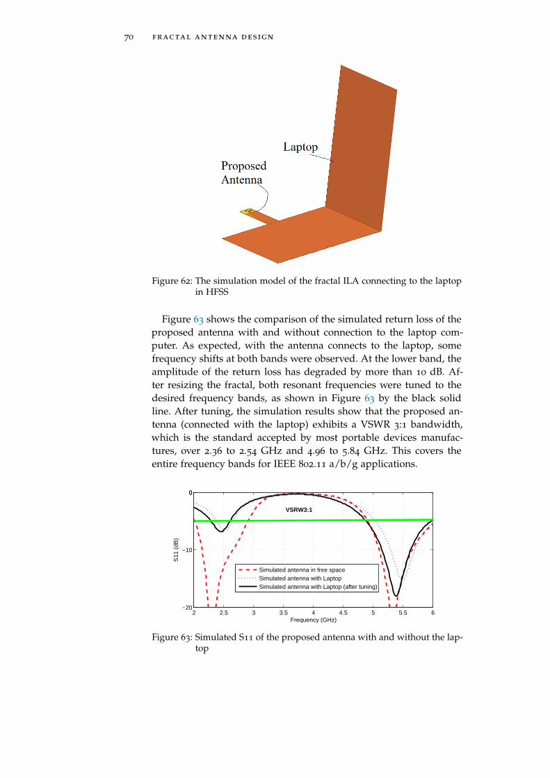
70 fractal antenna design
Figure 62: The simulation model of the fractal ILA connecting to the laptopin HFSS
Figure 63 shows the comparison of the simulated return loss of theproposed antenna with and without connection to the laptop com-puter. As expected, with the antenna connects to the laptop, somefrequency shifts at both bands were observed. At the lower band, theamplitude of the return loss has degraded by more than 10 dB. Af-ter resizing the fractal, both resonant frequencies were tuned to thedesired frequency bands, as shown in Figure 63 by the black solidline. After tuning, the simulation results show that the proposed an-tenna (connected with the laptop) exhibits a VSWR 3:1 bandwidth,which is the standard accepted by most portable devices manufac-tures, over 2.36 to 2.54 GHz and 4.96 to 5.84 GHz. This covers theentire frequency bands for IEEE 802.11 a/b/g applications.
2 2.5 3 3.5 4 4.5 5 5.5 6−20
−10
00
Frequency (GHz)
S11
(dB
)
Simulated antenna in free spaceSimulated antenna with LaptopSimulated antenna with Laptop (after tuning)
VSRW3:1
Figure 63: Simulated S11 of the proposed antenna with and without the lap-top
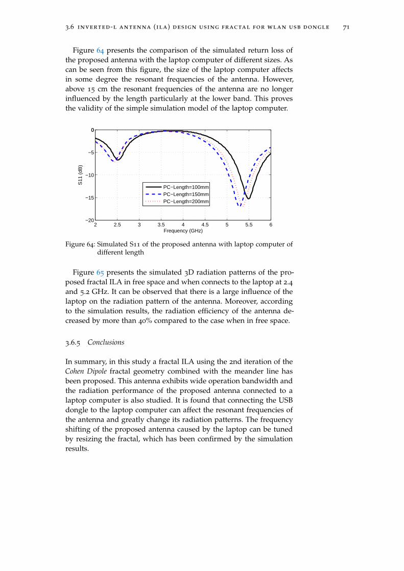
3.6 inverted-l antenna (ila) design using fractal for wlan usb dongle 71
Figure 64 presents the comparison of the simulated return loss ofthe proposed antenna with the laptop computer of different sizes. Ascan be seen from this figure, the size of the laptop computer affectsin some degree the resonant frequencies of the antenna. However,above 15 cm the resonant frequencies of the antenna are no longerinfluenced by the length particularly at the lower band. This provesthe validity of the simple simulation model of the laptop computer.
2 2.5 3 3.5 4 4.5 5 5.5 6−20
−15
−10
−5
00
Frequency (GHz)
S11
(dB
)
PC−Length=100mmPC−Length=150mmPC−Length=200mm
Figure 64: Simulated S11 of the proposed antenna with laptop computer ofdifferent length
Figure 65 presents the simulated 3D radiation patterns of the pro-posed fractal ILA in free space and when connects to the laptop at 2.4and 5.2 GHz. It can be observed that there is a large influence of thelaptop on the radiation pattern of the antenna. Moreover, accordingto the simulation results, the radiation efficiency of the antenna de-creased by more than 40% compared to the case when in free space.
3.6.5 Conclusions
In summary, in this study a fractal ILA using the 2nd iteration of theCohen Dipole fractal geometry combined with the meander line hasbeen proposed. This antenna exhibits wide operation bandwidth andthe radiation performance of the proposed antenna connected to alaptop computer is also studied. It is found that connecting the USBdongle to the laptop computer can affect the resonant frequencies ofthe antenna and greatly change its radiation patterns. The frequencyshifting of the proposed antenna caused by the laptop can be tunedby resizing the fractal, which has been confirmed by the simulationresults.
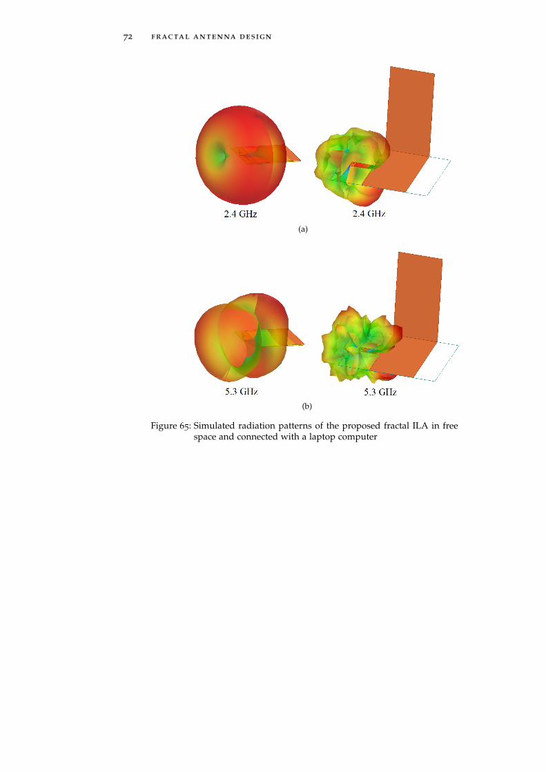
72 fractal antenna design
(a)
(b)
Figure 65: Simulated radiation patterns of the proposed fractal ILA in freespace and connected with a laptop computer

3.7 single feed fractal monopole antenna array 73
3.7 single feed fractal monopole antenna array
3.7.1 Motivation
To increase the directivity of a antenna system, the use of antennaarrays is an effective solution if an additional antenna element canbe added in the wireless device. A single feed antenna array has theadvantages of easy fabrication and does not need any extra RF com-ponents such has phase shifter. The objective of this work is to designone compact single feed multiband printed monopole antenna arrayfor WLAN dual band application. It is desirable to design such an-tenna in planar structure as it can simplify the fabrication processand reduce the fabrication cost. Based on the results of the previousstudies in Section 3.4, which confirms the size reduction and multi-ple frequency operation of the antenna using the fractal technique,the 2nd iteration of the Minkowski fractal geometry was chosen forthis design.
In [55, 56], two single feed circular polarized microstrip antennaarrays were presented. The concept behind these two designs is touse the antenna array to achieve circular polarization and improvethe directivity of the antenna. However, these two antennas have rel-atively large size and can only operate at a single frequency band.One printed single feed monopole antenna array has been reportedin [57]. In that design the antenna array contains three equally spacedequilateral triangular monopoles of different sizes, which contributeto the multiple resonant frequencies at 2 and 5 GHz bands. How-ever, the antenna in [57] is actually a multi-armed structure ratherthan a real array. The radiation performance of the antenna does notbenefit much from using such antenna array. In [58], two multibandprinted monopole antennas using the 1st and 2nd generation of theMinkowski fractal geometry were presented. The antennas have com-pact size and show multiband operation with wide bandwidth. How-ever, so far, there is not much work reported on the use of fractals todesign compact single feed printed monopole antenna arrays.
One common problem that is always encountered during the de-sign of multiband antenna is how to improve the impedance match-ing at multiple resonant frequencies. In [59], band broadening wasachieved through the use of a rectangular monopole backed by atrapezoid conductor. However, this method can greatly change theresonant frequency of original antenna and the size of the trapezoidis very critical, which is not easy to optimize. Reference [60] shows anexample of designing a multiband printed monopole antenna usingGenetic Algorithm. Although the antenna has a wide operation band,it has a complicated pattern and the impedance matching improve-ment was achieved through repetitive numerical simulations. In thiswork, these limitations are overcomed by adding a rectangular stub
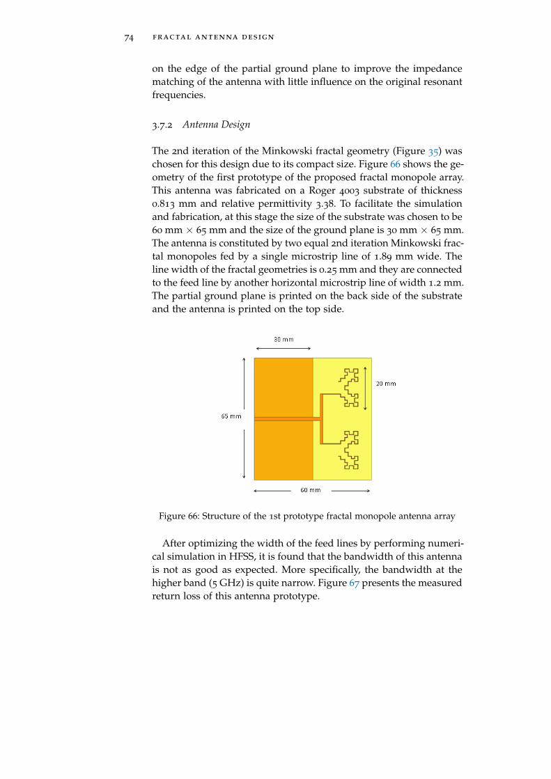
74 fractal antenna design
on the edge of the partial ground plane to improve the impedancematching of the antenna with little influence on the original resonantfrequencies.
3.7.2 Antenna Design
The 2nd iteration of the Minkowski fractal geometry (Figure 35) waschosen for this design due to its compact size. Figure 66 shows the ge-ometry of the first prototype of the proposed fractal monopole array.This antenna was fabricated on a Roger 4003 substrate of thickness0.813 mm and relative permittivity 3.38. To facilitate the simulationand fabrication, at this stage the size of the substrate was chosen to be60 mm × 65 mm and the size of the ground plane is 30 mm × 65 mm.The antenna is constituted by two equal 2nd iteration Minkowski frac-tal monopoles fed by a single microstrip line of 1.89 mm wide. Theline width of the fractal geometries is 0.25 mm and they are connectedto the feed line by another horizontal microstrip line of width 1.2 mm.The partial ground plane is printed on the back side of the substrateand the antenna is printed on the top side.
Figure 66: Structure of the 1st prototype fractal monopole antenna array
After optimizing the width of the feed lines by performing numeri-cal simulation in HFSS, it is found that the bandwidth of this antennais not as good as expected. More specifically, the bandwidth at thehigher band (5 GHz) is quite narrow. Figure 67 presents the measuredreturn loss of this antenna prototype.
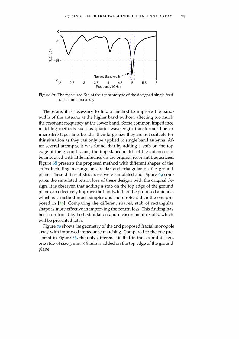
3.7 single feed fractal monopole antenna array 75
2 2.5 3 3.5 4 4.5 5 5.5 6−25
−15
−5
00
Frequency (GHz)
S11
(dB
)
Narrow Bandwidth
Figure 67: The measured S11 of the 1st prototype of the designed single feedfractal antenna array
Therefore, it is necessary to find a method to improve the band-width of the antenna at the higher band without affecting too muchthe resonant frequency at the lower band. Some common impedancematching methods such as quarter-wavelength transformer line ormicrostrip taper line, besides their large size they are not suitable forthis situation as they can only be applied to single band antenna. Af-ter several attempts, it was found that by adding a stub on the topedge of the ground plane, the impedance match of the antenna canbe improved with little influence on the original resonant frequencies.Figure 68 presents the proposed method with different shapes of thestubs including rectangular, circular and triangular on the groundplane. These different structures were simulated and Figure 69 com-pares the simulated return loss of these designs with the original de-sign. It is observed that adding a stub on the top edge of the groundplane can effectively improve the bandwidth of the proposed antenna,which is a method much simpler and more robust than the one pro-posed in [59]. Comparing the different shapes, stub of rectangularshape is more effective in improving the return loss. This finding hasbeen confirmed by both simulation and measurement results, whichwill be presented later.
Figure 70 shows the geometry of the 2nd proposed fractal monopolearray with improved impedance matching. Compared to the one pre-sented in Figure 66, the only difference is that in the second design,one stub of size 3 mm × 8 mm is added on the top edge of the groundplane.
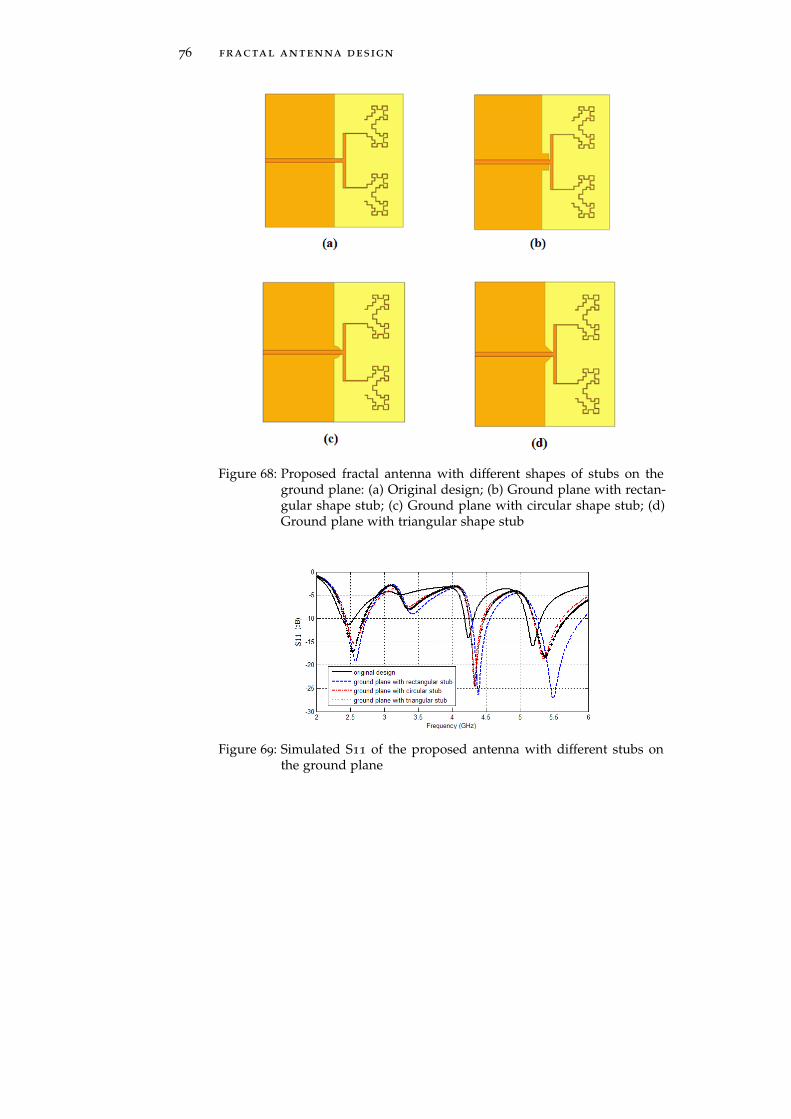
76 fractal antenna design
Figure 68: Proposed fractal antenna with different shapes of stubs on theground plane: (a) Original design; (b) Ground plane with rectan-gular shape stub; (c) Ground plane with circular shape stub; (d)Ground plane with triangular shape stub
Figure 69: Simulated S11 of the proposed antenna with different stubs onthe ground plane
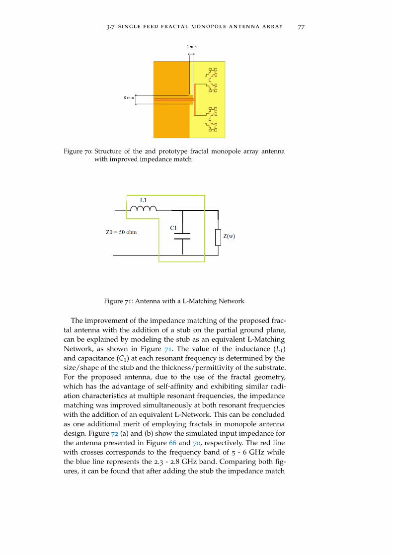
3.7 single feed fractal monopole antenna array 77
Figure 70: Structure of the 2nd prototype fractal monopole array antennawith improved impedance match
Figure 71: Antenna with a L-Matching Network
The improvement of the impedance matching of the proposed frac-tal antenna with the addition of a stub on the partial ground plane,can be explained by modeling the stub as an equivalent L-MatchingNetwork, as shown in Figure 71. The value of the inductance (L1)and capacitance (C1) at each resonant frequency is determined by thesize/shape of the stub and the thickness/permittivity of the substrate.For the proposed antenna, due to the use of the fractal geometry,which has the advantage of self-affinity and exhibiting similar radi-ation characteristics at multiple resonant frequencies, the impedancematching was improved simultaneously at both resonant frequencieswith the addition of an equivalent L-Network. This can be concludedas one additional merit of employing fractals in monopole antennadesign. Figure 72 (a) and (b) show the simulated input impedance forthe antenna presented in Figure 66 and 70, respectively. The red linewith crosses corresponds to the frequency band of 5 - 6 GHz whilethe blue line represents the 2.3 - 2.8 GHz band. Comparing both fig-ures, it can be found that after adding the stub the impedance match
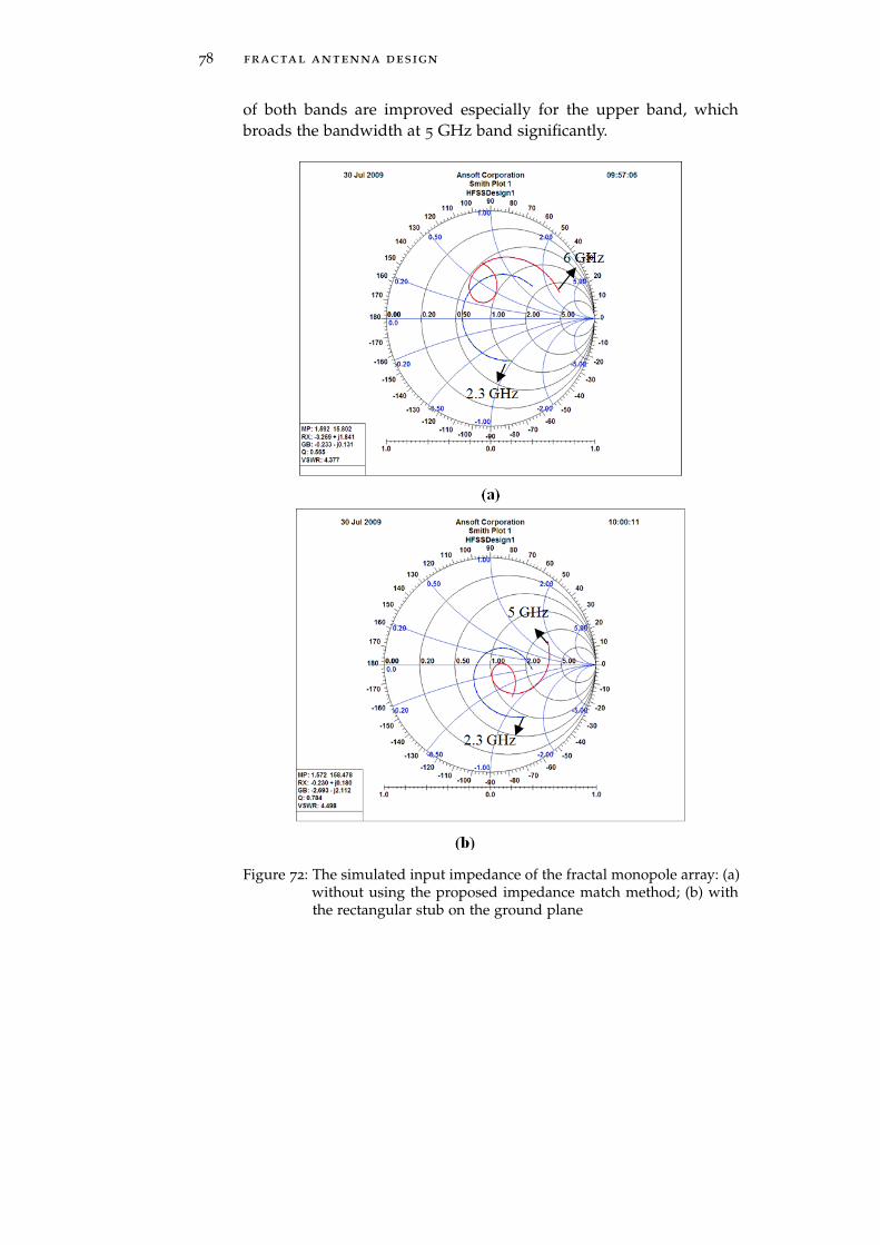
78 fractal antenna design
of both bands are improved especially for the upper band, whichbroads the bandwidth at 5 GHz band significantly.
Figure 72: The simulated input impedance of the fractal monopole array: (a)without using the proposed impedance match method; (b) withthe rectangular stub on the ground plane
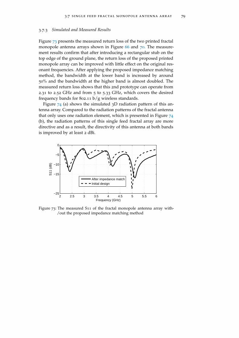
3.7 single feed fractal monopole antenna array 79
3.7.3 Simulated and Measured Results
Figure 73 presents the measured return loss of the two printed fractalmonopole antenna arrays shown in Figure 66 and 70. The measure-ment results confirm that after introducing a rectangular stub on thetop edge of the ground plane, the return loss of the proposed printedmonopole array can be improved with little effect on the original res-onant frequencies. After applying the proposed impedance matchingmethod, the bandwidth at the lower band is increased by around50% and the bandwidth at the higher band is almost doubled. Themeasured return loss shows that this 2nd prototype can operate from2.31 to 2.52 GHz and from 5 to 5.33 GHz, which covers the desiredfrequency bands for 802.11 b/g wireless standards.
Figure 74 (a) shows the simulated 3D radiation pattern of this an-tenna array. Compared to the radiation patterns of the fractal antennathat only uses one radiation element, which is presented in Figure 74
(b), the radiation patterns of this single feed fractal array are moredirective and as a result, the directivity of this antenna at both bandsis improved by at least 2 dBi.
2 2.5 3 3.5 4 4.5 5 5.5 6−25
−15
−5
0
−10
Frequency (GHz)
S11
(dB
)
After impedance matchInitial design
Figure 73: The measured S11 of the fractal monopole antenna array with-/out the proposed impedance matching method
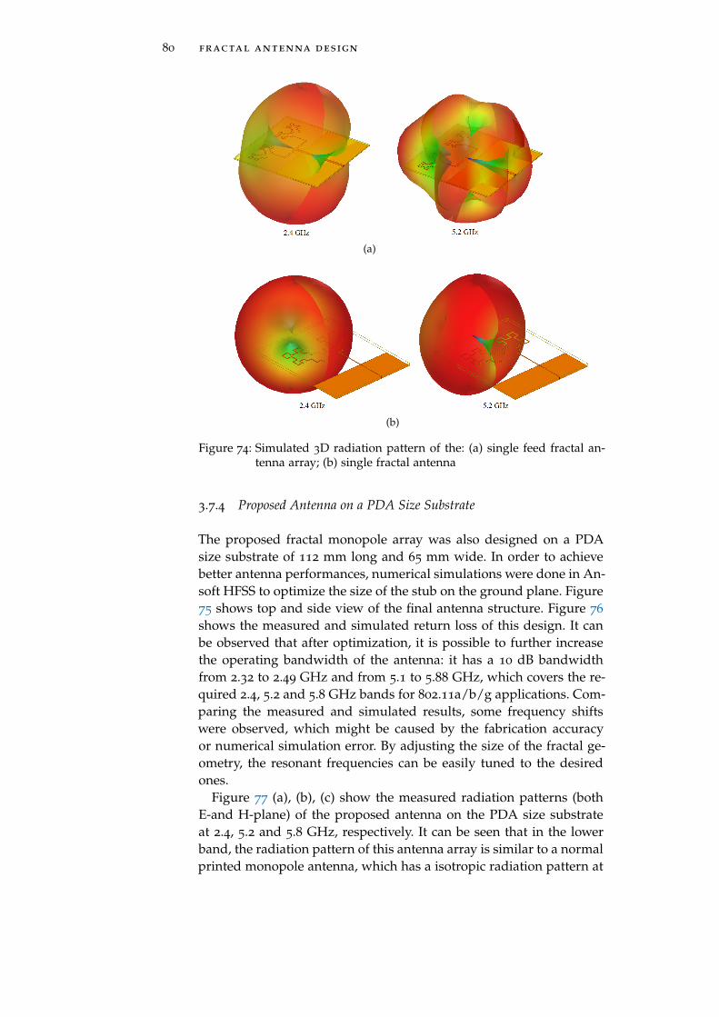
80 fractal antenna design
(a)
(b)
Figure 74: Simulated 3D radiation pattern of the: (a) single feed fractal an-tenna array; (b) single fractal antenna
3.7.4 Proposed Antenna on a PDA Size Substrate
The proposed fractal monopole array was also designed on a PDAsize substrate of 112 mm long and 65 mm wide. In order to achievebetter antenna performances, numerical simulations were done in An-soft HFSS to optimize the size of the stub on the ground plane. Figure75 shows top and side view of the final antenna structure. Figure 76
shows the measured and simulated return loss of this design. It canbe observed that after optimization, it is possible to further increasethe operating bandwidth of the antenna: it has a 10 dB bandwidthfrom 2.32 to 2.49 GHz and from 5.1 to 5.88 GHz, which covers the re-quired 2.4, 5.2 and 5.8 GHz bands for 802.11a/b/g applications. Com-paring the measured and simulated results, some frequency shiftswere observed, which might be caused by the fabrication accuracyor numerical simulation error. By adjusting the size of the fractal ge-ometry, the resonant frequencies can be easily tuned to the desiredones.
Figure 77 (a), (b), (c) show the measured radiation patterns (bothE-and H-plane) of the proposed antenna on the PDA size substrateat 2.4, 5.2 and 5.8 GHz, respectively. It can be seen that in the lowerband, the radiation pattern of this antenna array is similar to a normalprinted monopole antenna, which has a isotropic radiation pattern at
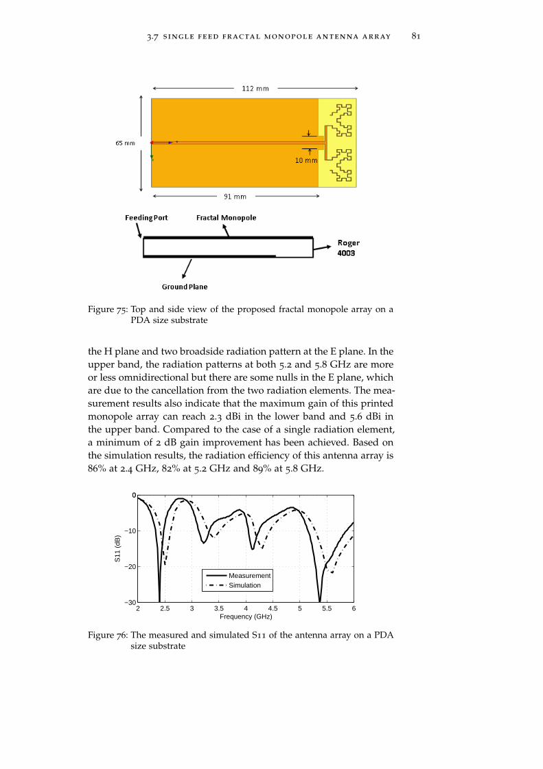
3.7 single feed fractal monopole antenna array 81
Figure 75: Top and side view of the proposed fractal monopole array on aPDA size substrate
the H plane and two broadside radiation pattern at the E plane. In theupper band, the radiation patterns at both 5.2 and 5.8 GHz are moreor less omnidirectional but there are some nulls in the E plane, whichare due to the cancellation from the two radiation elements. The mea-surement results also indicate that the maximum gain of this printedmonopole array can reach 2.3 dBi in the lower band and 5.6 dBi inthe upper band. Compared to the case of a single radiation element,a minimum of 2 dB gain improvement has been achieved. Based onthe simulation results, the radiation efficiency of this antenna array is86% at 2.4 GHz, 82% at 5.2 GHz and 89% at 5.8 GHz.
2 2.5 3 3.5 4 4.5 5 5.5 6−30
−20
−10
00
Frequency (GHz)
S11
(dB
)
MeasurementSimulation
Figure 76: The measured and simulated S11 of the antenna array on a PDAsize substrate
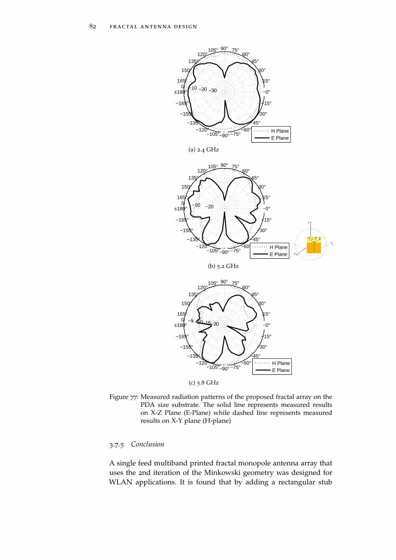
82 fractal antenna design
0°
15°
30°
45°60°
75°90°105°120°
135°
150°
165°
±180°
−165°
−150°
−135°−120°
−105°−90° −75°−60°
−45°
−30°
−15°
−30−20−100
H PlaneE Plane
(a) 2.4 GHz
0°
15°
30°
45°60°
75°90°105°120°
135°
150°
165°
±180°
−165°
−150°
−135°−120°
−105°−90° −75°−60°
−45°
−30°
−15°
−20−100
H PlaneE Plane
(b) 5.2 GHz
0°
15°
30°
45°60°
75°90°105°120°
135°
150°
165°
±180°
−165°
−150°
−135°−120°
−105°−90° −75°−60°
−45°
−30°
−15°
−20−15−10−50
H PlaneE Plane
(c) 5.8 GHz
Figure 77: Measured radiation patterns of the proposed fractal array on thePDA size substrate. The solid line represents measured resultson X-Z Plane (E-Plane) while dashed line represents measuredresults on X-Y plane (H-plane)
3.7.5 Conclusion
A single feed multiband printed fractal monopole antenna array thatuses the 2nd iteration of the Minkowski geometry was designed forWLAN applications. It is found that by adding a rectangular stub
3.8 summary of the chapter 83
on the edge of the partial ground plane, the impedance match atboth bands (2 and 5 GHz) can be improved with little influence onthe original resonant frequencies, which has been confirmed by bothsimulation and experiment results. Moreover, the proposed antennageometry was designed on a PDA size substrate. The experimentalresults show that this antenna has wide operation bandwidth in bothbands and has a 2 dB gain improvement compared to the antennawith only one radiation element.
3.8 summary of the chapter
In this chapter, the fractal techniques have been employed to thedesign of compact multiband printed monopole antennas. A set ofMATLAB functions were developed to aid the modeling of fractalstructures in Ansoft HFSS. This methodology utilizes recursive func-tions to calculate the coordinates of each node of the fractals and thenwrite a vbs file that can be executed by the EM simulation software tocreate fractals in simulation environment with required physical di-mensions. Then, based on this tool, three multiband fractal monopoleantennas, one fractal-based Inverted-L antenna and one single feedfractal monopole antenna array are proposed, all of which were de-signed for the dual or triple bands WLAN application. The experi-mental results confirm the advantages of fractal antennas: compactsize, multi-frequency operation and wide operation bandwidth. Thepublications resulted from the work presented in this chapter are:
1. Qi Luo; Jose Pereira and Henrique Salgado. Inverted-L Antenna(ILA) Design using Fractal for WLAN USB Dongle. In Proceed-ings of Conference on Electronics, Telecommunications and Comput-ers, Lisbon, Portugal, November 2011.
2. Q. Luo; H.M. Salgado and J.R. Pereira. Printed Fractal MonopoleAntenna Array For WLAN. In Proceedings of International Work-shop on Antenna Technology (iWAT), Lisbon, Portugal, March 2010.
3. Q. Luo; J.R. Pereira and H. Salgado. Fractal Monopole AntennaFor WLAN USB Dongle. In Proceedings of Loughborough Antennasand Propagation Conference, vol. 1, pp. 245-247, Loughborough,UK, November 2009.
4. Q. Luo; H. M. Salgado and J. R. Pereira. Fractal Monopole An-tenna Design Using Minkowski Island Geometry. In Proceed-ings of IEEE International Symposium on Antennas and Propagation,Charleston, United States, June 2009.

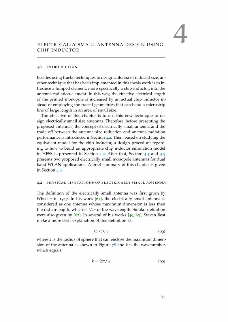
4E L E C T R I C A L LY S M A L L A N T E N N A D E S I G N U S I N GC H I P I N D U C T O R
4.1 introduction
Besides using fractal techniques to design antenna of reduced size, an-other technique that has been implemented in this thesis work is to in-troduce a lumped element, more specifically a chip inductor, into theantenna radiation element. In this way, the effective electrical lengthof the printed monopole is increased by an actual chip inductor in-stead of employing the fractal geometries that can bend a microstripline of large length in an area of small size.
The objective of this chapter is to use this new technique to de-sign electrically small size antennas. Therefore, before presenting theproposed antennas, the concept of electrically small antenna and thetrade-off between the antenna size reduction and antenna radiationperformance is introduced in Section 4.2. Then, based on studying theequivalent model for the chip inductor, a design procedure regard-ing to how to build an appropriate chip inductor simulation modelin HFSS is presented in Section 4.3. After that, Section 4.4 and 4.5presents two proposed electrically small monopole antennas for dualband WLAN applications. A brief summary of this chapter is givenin Section 4.6.
4.2 physical limitations of electrically small antenna
The definition of the electrically small antenna was first given byWheeler in 1947. In his work [61], the electrically small antenna isconsidered as one antenna whose maximum dimension is less thanthe radian-length, which is 1/2π of the wavelength. Similar definitionwere also given by [62]. In several of his works [49, 63], Steven Bestmake a more clear explanation of this definition as:
ka < 0.5 (89)
where a is the radius of sphere that can enclose the maximum dimen-sion of the antenna as shown in Figure 78 and k is the wavenumber,which equals:
k = 2π/λ (90)
85
86 electrically small antenna design using chip inductor
Figure 78: A dipole antenna enclosed in a sphere with radius of a
According to [61], the antenna within this size limit can be made tobehave as a lumped capacitor or inductor and the fundamental limita-tion on the bandwidth and the efficiency of a small antenna is relatedto the radiation power factor, pe or pm, which can be represented by
pe =Ge
wC(91)
when the antenna is made to behave as a lumped capacitor or by
pm =Rm
wL(92)
when it behaves as a inductor, where Ge is the radiation conductancein parallel with antenna, Rm is the radiation resistance in series withantenna, w is the radian frequency, C is the capacitance of antennaand L is the inductance of the antenna.
The limitations of the electrically small antennas was also inves-tigated by Chu [64]. By investigating the equivalent circuit modelsfor an electric dipole and employing the TM and TE spherical wavemodes, the limits of quality factor (Q) of an antenna was calculatedand shown to be inversely proportional to the size of the antenna.Assuming there is one equivalent circuit that gives a good approxi-mation to the antenna and it has fixed values at antenna’s operationfrequency, according to the study presented in [65], the bandwidth ofthe antenna can be related to the Q as:
Bandwidth =1Q
(93)
The equation is relatively accurate when Q 1. When Q < 2, thisequation fails to provide a precise results. However, the relationshipbetween bandwidth and Q still stands, which means that the band-width of one antenna is always inversely proportional to its Q. Theminimum value of Q that one antenna can exhibit was further stud-
4.2 physical limitations of electrically small antenna 87
ied in [66] and in this study a formula to calculate the lower boundof the quality factor was derived:
Qlb =
[1
(ka)3 +1ka
](94)
Equation 94 gives the lower bound of the Q factor for a linearly po-larized antenna and it agrees with the calculation results using Chu’sequivalent circuit model. The exact value of the Q of one antenna canbe calculated using the expression given in [67]:
Q(ω0) = |ω0
2R0(ω0)X′0(ω0)−
2ω0
|I0|2R0(ω0)[WL(ω0) + WR(ω0)]| (95)
where w0 is the radian frequency, I0 represents the current propa-gated on the antenna, WL(ω) is the energy lost on the antenna andWR(ω) is the energy radiated by the antenna. R(ω) and X(ω) arethe real part and imaginary part of the complex input impedance ofthe antenna, respectively. Through some mathematical manipulation,[67] simplified Equation 95 into the following equations:
Q(ω0) =2√
β
FBWv(ω0)(96)
where
FBWv(ω0) =ω+ −ω−
ω0(97)
√β =
s− 12√
s(98)
The parameter s is the criterion for the maximum VSWR and ω+,ω−, ω0 represent the higher frequency bound, lower frequency boundand central frequency of the antenna, respectively. This gives a goodapproximation of the actual value of the Q at both resonant and anti-resonant frequencies compared to the one given in [64] and has beenwidely accepted by most researchers. Moreover, the authors in [67]redefined a more accurate formula to calculate the lower bound of thequality factor of the antenna by introducing the radiation efficiencyηr:
Qlb =
[1
(ka)3 +1ka
]ηr (99)
As can be seen from the above equations, the antenna of smallersize always exhibits a higher quality factor. However, the bandwidthof an antenna is inversely proportional to the value of quality fac-tor, which means that the size reduction of one antenna will lead toa narrow band antenna design. Although introducing losses to the
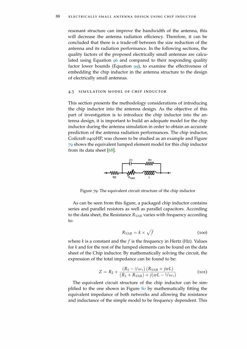
88 electrically small antenna design using chip inductor
resonant structure can improve the bandwidth of the antenna, thiswill decrease the antenna radiation efficiency. Therefore, it can beconcluded that there is a trade-off between the size reduction of theantenna and its radiation performance. In the following sections, thequality factors of the proposed electrically small antennas are calcu-lated using Equation 96 and compared to their responding qualityfactor lower bounds (Equation 99), to examine the effectiveness ofembedding the chip inductor in the antenna structure to the designof electrically small antennas.
4.3 simulation model of chip inductor
This section presents the methodology considerations of introducingthe chip inductor into the antenna design. As the objective of thispart of investigation is to introduce the chip inductor into the an-tenna design, it is important to build an adequate model for the chipinductor during the antenna simulation in order to obtain an accurateprediction of the antenna radiation performances. The chip inductor,Coilcraft 0402HP, was chosen to be studied as an example and Figure79 shows the equivalent lumped element model for this chip inductorfrom its data sheet [68].
Figure 79: The equivalent circuit structure of the chip inductor
As can be seen from this figure, a packaged chip inductor containsseries and parallel resistors as well as parallel capacitors. Accordingto the data sheet, the Resistance RVAR varies with frequency accordingto:
RVAR = k×√
f (100)
where k is a constant and the f is the frequency in Hertz (Hz). Valuesfor k and for the rest of the lumped elements can be found on the datasheet of the Chip inductor. By mathematically solving the circuit, theexpression of the total impedance can be found to be:
Z = R2 +(R1 − j/wc1) (RVAR + jwL)
(R1 + RVAR) + j(wL− 1/wc1)(101)
The equivalent circuit structure of the chip inductor can be sim-plified to the one shown in Figure 80 by mathematically fitting theequivalent impedance of both networks and allowing the resistanceand inductance of the simple model to be frequency dependent. This
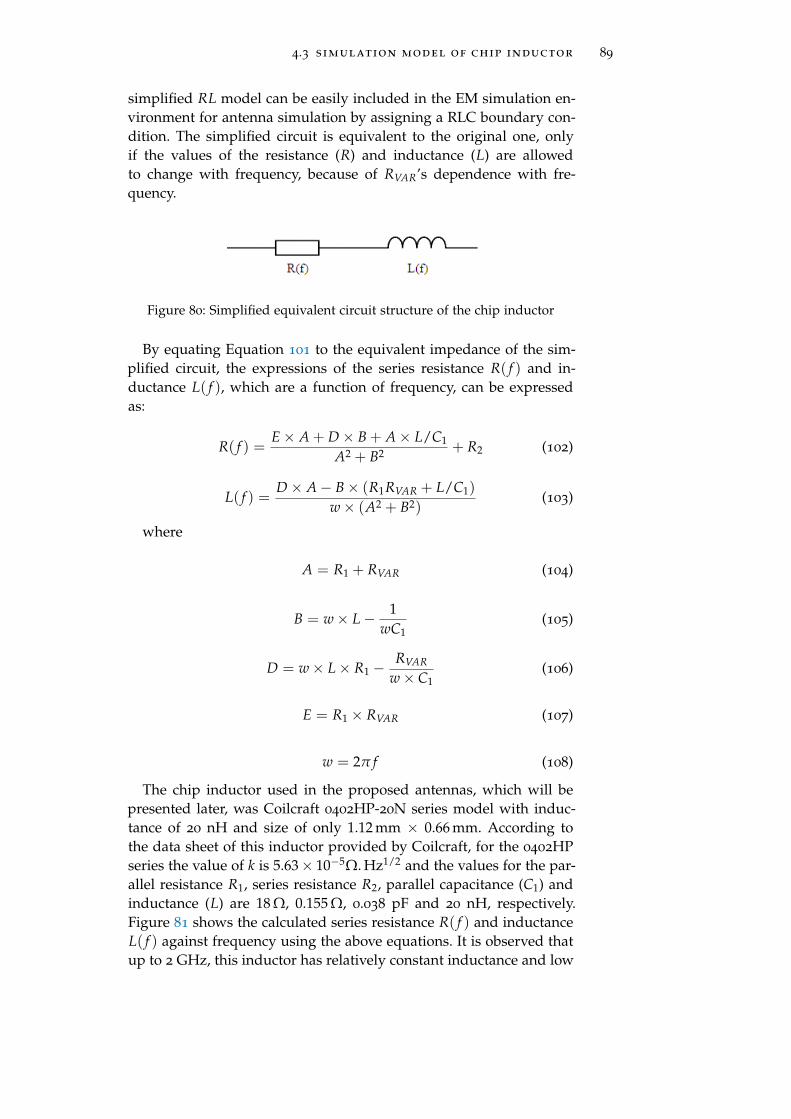
4.3 simulation model of chip inductor 89
simplified RL model can be easily included in the EM simulation en-vironment for antenna simulation by assigning a RLC boundary con-dition. The simplified circuit is equivalent to the original one, onlyif the values of the resistance (R) and inductance (L) are allowedto change with frequency, because of RVAR’s dependence with fre-quency.
Figure 80: Simplified equivalent circuit structure of the chip inductor
By equating Equation 101 to the equivalent impedance of the sim-plified circuit, the expressions of the series resistance R( f ) and in-ductance L( f ), which are a function of frequency, can be expressedas:
R( f ) =E× A + D× B + A× L/C1
A2 + B2 + R2 (102)
L( f ) =D× A− B× (R1RVAR + L/C1)
w× (A2 + B2)(103)
where
A = R1 + RVAR (104)
B = w× L− 1wC1
(105)
D = w× L× R1 −RVAR
w× C1(106)
E = R1 × RVAR (107)
w = 2π f (108)
The chip inductor used in the proposed antennas, which will bepresented later, was Coilcraft 0402HP-20N series model with induc-tance of 20 nH and size of only 1.12 mm × 0.66 mm. According tothe data sheet of this inductor provided by Coilcraft, for the 0402HPseries the value of k is 5.63× 10⁻⁵Ω. Hz1/2 and the values for the par-allel resistance R1, series resistance R2, parallel capacitance (C1) andinductance (L) are 18 Ω, 0.155 Ω, 0.038 pF and 20 nH, respectively.Figure 81 shows the calculated series resistance R( f ) and inductanceL( f ) against frequency using the above equations. It is observed thatup to 2 GHz, this inductor has relatively constant inductance and low
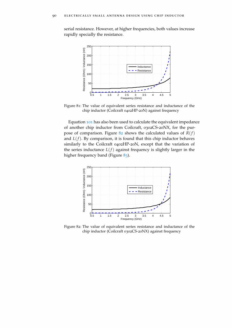
90 electrically small antenna design using chip inductor
serial resistance. However, at higher frequencies, both values increaserapidly specially the resistance.
0.5 1 1.5 2 2.5 3 3.5 4 4.5 50
50
100
150
200
250
Frequency (GHz)
Res
ista
nce
(Ohm
) / i
nduc
tanc
e (n
H)
InductanceResistance
Figure 81: The value of equivalent series resistance and inductance of thechip inductor (Coilcraft 0402HP-20N) against frequency
Equation 101 has also been used to calculate the equivalent impedanceof another chip inductor from Coilcraft, 0302CS-20NX, for the pur-pose of comparison. Figure 82 shows the calculated values of R( f )and L( f ). By comparison, it is found that this chip inductor behavessimilarly to the Coilcraft 0402HP-20N, except that the variation ofthe series inductance L( f ) against frequency is slightly larger in thehigher frequency band (Figure 83).
0.5 1 1.5 2 2.5 3 3.5 4 4.5 50
50
100
150
200
250
Frequency (GHz)
Res
ista
nce
(Ohm
) / i
nduc
tanc
e (n
H)
InductanceResistance
Figure 82: The value of equivalent series resistance and inductance of thechip inductor (Coilcraft 0302CS-20NX) against frequency
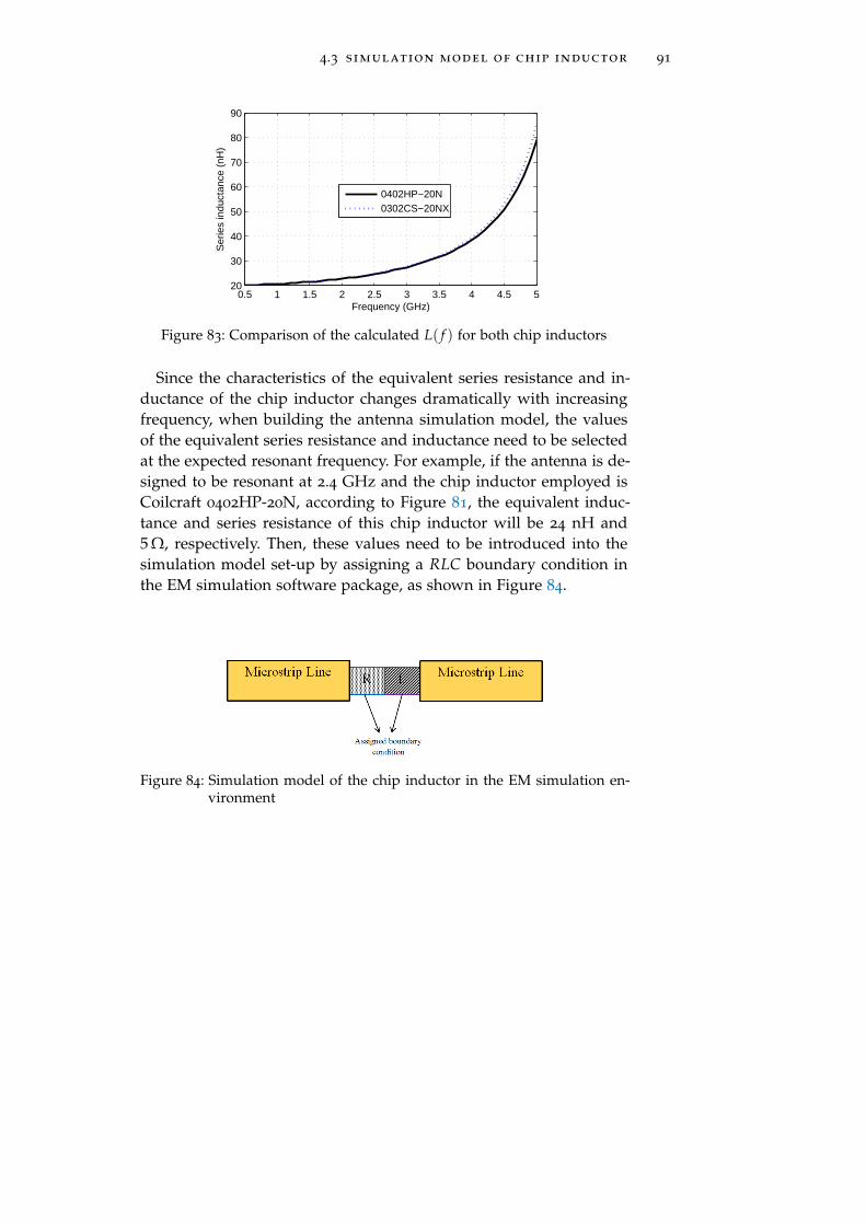
4.3 simulation model of chip inductor 91
0.5 1 1.5 2 2.5 3 3.5 4 4.5 520
30
40
50
60
70
80
90
Frequency (GHz)
Ser
ies
indu
ctan
ce (
nH)
0402HP−20N0302CS−20NX
Figure 83: Comparison of the calculated L( f ) for both chip inductors
Since the characteristics of the equivalent series resistance and in-ductance of the chip inductor changes dramatically with increasingfrequency, when building the antenna simulation model, the valuesof the equivalent series resistance and inductance need to be selectedat the expected resonant frequency. For example, if the antenna is de-signed to be resonant at 2.4 GHz and the chip inductor employed isCoilcraft 0402HP-20N, according to Figure 81, the equivalent induc-tance and series resistance of this chip inductor will be 24 nH and5 Ω, respectively. Then, these values need to be introduced into thesimulation model set-up by assigning a RLC boundary condition inthe EM simulation software package, as shown in Figure 84.
Figure 84: Simulation model of the chip inductor in the EM simulation en-vironment
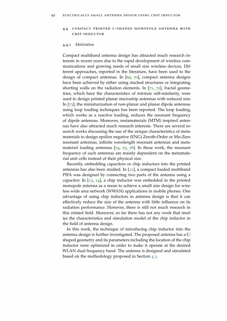
92 electrically small antenna design using chip inductor
4.4 compact printed c-shaped monopole antenna with
chip inductor
4.4.1 Motivation
Compact multiband antenna design has attracted much research in-terests in recent years due to the rapid development of wireless com-munications and growing needs of small size wireless devices. Dif-ferent approaches, reported in the literature, have been used to thedesign of compact antennas. In [69, 70], compact antenna designshave been achieved by either using stacked structures or integratingshorting walls on the radiation elements. In [71, 72], fractal geome-tries, which have the characteristics of intrinsic self-similarity, wereused to design printed planar microstrip antennas with reduced size.In [73], the miniaturization of non-planar and planar dipole antennasusing loop loading techniques has been reported. The loop loading,which works as a reactive loading, reduces the resonant frequencyof dipole antennas. Moreover, metamaterials (MTM) inspired anten-nas have also attracted much research interests. There are several re-search works discussing the use of the unique characteristics of meta-materials to design epsilon negative (ENG) Zeroth-Order or Mu-Zeroresonant antennas, infinite wavelength resonant antennas and meta-material loading antennas [74, 75, 76]. In these work, the resonantfrequency of such antennas are mainly dependent on the metamate-rial unit cells instead of their physical size.
Recently, embedding capacitors or chip inductors into the printedantennas has also been studied. In [11], a compact loaded multibandPIFA was designed by connecting two parts of the antenna using acapacitor. In [13, 14], a chip inductor was embedded in the printedmonopole antenna as a mean to achieve a small size design for wire-less wide area network (WWAN) applications in mobile phones. Oneadvantage of using chip inductors in antenna design is that it caneffectively reduce the size of the antenna with little influence on itsradiation performance. However, there is still not much research inthis related field. Moreover, so far there has not any work that stud-ies the characteristics and simulation model of the chip inductor inthe field of antenna design.
In this work, the technique of introducing chip inductor into theantenna design is further investigated. The proposed antenna has a C-shaped geometry and its parameters including the location of the chipinductor were optimized in order to make it operate at the desiredWLAN dual frequency band. The antenna is designed and simulatedbased on the methodology proposed in Section 4.3.
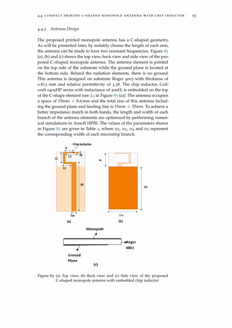
4.4 compact printed c-shaped monopole antenna with chip inductor 93
4.4.2 Antenna Design
The proposed printed monopole antenna has a C-shaped geometry.As will be presented later, by suitably choose the length of each arm,the antenna can be made to have two resonant frequencies. Figure 85
(a), (b) and (c) shows the top view, back view and side view of the pro-posed C-shaped monopole antenna. The antenna element is printedon the top side of the substrate while the ground plane is located atthe bottom side. Behind the radiation elements, there is no ground.This antenna is designed on substrate Roger 4003 with thickness of0.813 mm and relative permittivity of 3.38. The chip inductor, Coil-craft 0402HP series with inductance of 20nH, is embedded on the topof the C-shape element (see L3 in Figure 85 (a)). The antenna occupiesa space of 15mm × 8.6 mm and the total size of this antenna includ-ing the ground plane and feeding line is 15mm × 35mm. To achieve abetter impedance match in both bands, the length and width of eachbranch of the antenna elements are optimized by performing numer-ical simulations in Ansoft HFSS. The values of the parameters shownin Figure 85 are given in Table 2, where w2, w3, w4 and w5 representthe corresponding width of each microstrip branch.
Figure 85: (a) Top view, (b) Back view and (c) Side view of the proposedC-shaped monopole antenna with embedded chip inductor
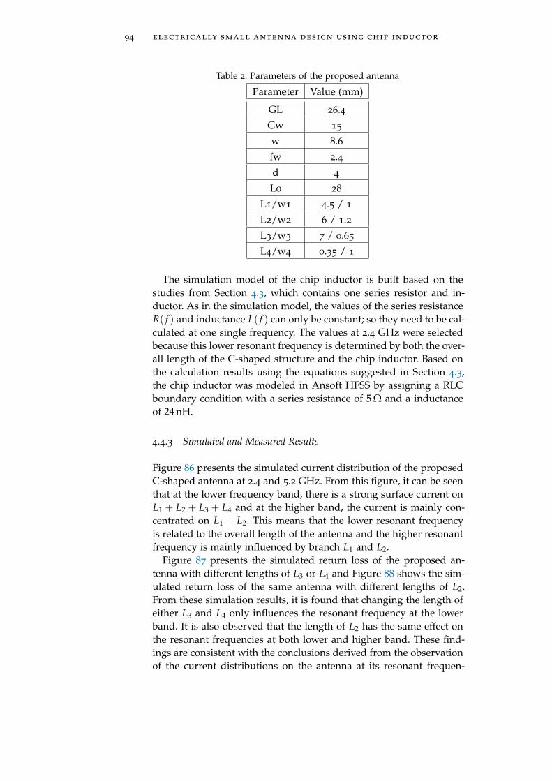
94 electrically small antenna design using chip inductor
Table 2: Parameters of the proposed antenna
Parameter Value (mm)
GL 26.4
Gw 15
w 8.6
fw 2.4
d 4
L0 28
L1/w1 4.5 / 1
L2/w2 6 / 1.2
L3/w3 7 / 0.65
L4/w4 0.35 / 1
The simulation model of the chip inductor is built based on thestudies from Section 4.3, which contains one series resistor and in-ductor. As in the simulation model, the values of the series resistanceR( f ) and inductance L( f ) can only be constant; so they need to be cal-culated at one single frequency. The values at 2.4 GHz were selectedbecause this lower resonant frequency is determined by both the over-all length of the C-shaped structure and the chip inductor. Based onthe calculation results using the equations suggested in Section 4.3,the chip inductor was modeled in Ansoft HFSS by assigning a RLCboundary condition with a series resistance of 5 Ω and a inductanceof 24 nH.
4.4.3 Simulated and Measured Results
Figure 86 presents the simulated current distribution of the proposedC-shaped antenna at 2.4 and 5.2 GHz. From this figure, it can be seenthat at the lower frequency band, there is a strong surface current onL1 + L2 + L3 + L4 and at the higher band, the current is mainly con-centrated on L1 + L2. This means that the lower resonant frequencyis related to the overall length of the antenna and the higher resonantfrequency is mainly influenced by branch L1 and L2.
Figure 87 presents the simulated return loss of the proposed an-tenna with different lengths of L3 or L4 and Figure 88 shows the sim-ulated return loss of the same antenna with different lengths of L2.From these simulation results, it is found that changing the length ofeither L3 and L4 only influences the resonant frequency at the lowerband. It is also observed that the length of L2 has the same effect onthe resonant frequencies at both lower and higher band. These find-ings are consistent with the conclusions derived from the observationof the current distributions on the antenna at its resonant frequen-
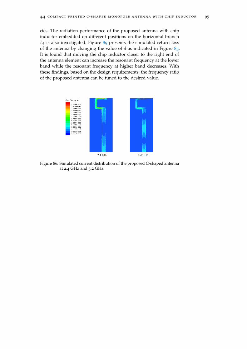
4.4 compact printed c-shaped monopole antenna with chip inductor 95
cies. The radiation performance of the proposed antenna with chipinductor embedded on different positions on the horizontal branchL3 is also investigated. Figure 89 presents the simulated return lossof the antenna by changing the value of d as indicated in Figure 85.It is found that moving the chip inductor closer to the right end ofthe antenna element can increase the resonant frequency at the lowerband while the resonant frequency at higher band decreases. Withthese findings, based on the design requirements, the frequency ratioof the proposed antenna can be tuned to the desired value.
Figure 86: Simulated current distribution of the proposed C-shaped antennaat 2.4 GHz and 5.2 GHz
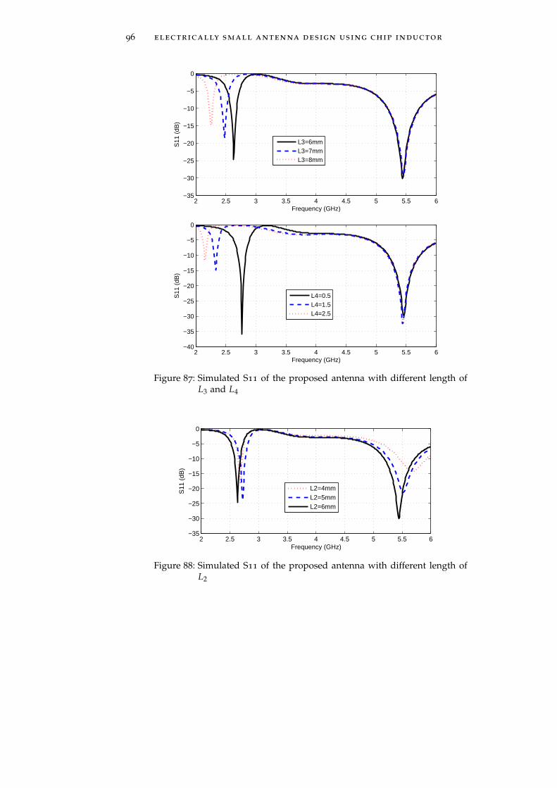
96 electrically small antenna design using chip inductor
2 2.5 3 3.5 4 4.5 5 5.5 6−35
−30
−25
−20
−15
−10
−5
0
Frequency (GHz)
S11
(dB
)
L3=6mmL3=7mmL3=8mm
2 2.5 3 3.5 4 4.5 5 5.5 6−40
−35
−30
−25
−20
−15
−10
−5
0
Frequency (GHz)
S11
(dB
)
L4=0.5L4=1.5L4=2.5
Figure 87: Simulated S11 of the proposed antenna with different length ofL3 and L4
2 2.5 3 3.5 4 4.5 5 5.5 6−35
−30
−25
−20
−15
−10
−5
0
Frequency (GHz)
S11
(dB
)
L2=4mmL2=5mmL2=6mm
Figure 88: Simulated S11 of the proposed antenna with different length ofL2
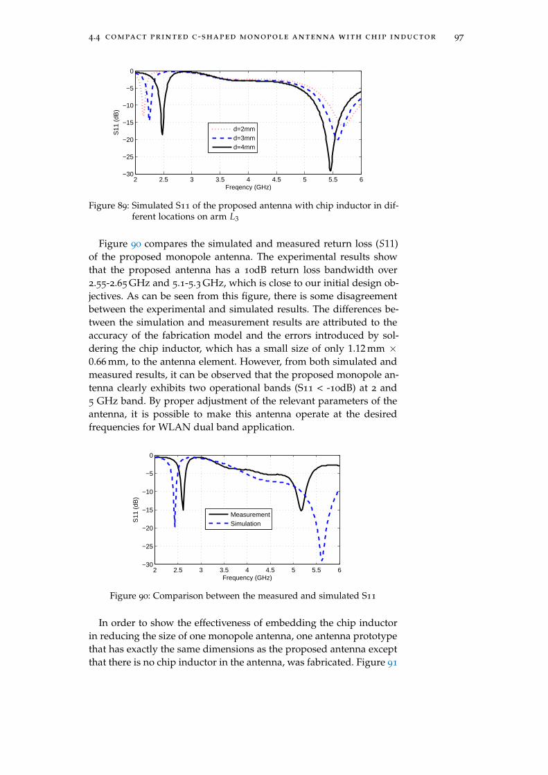
4.4 compact printed c-shaped monopole antenna with chip inductor 97
2 2.5 3 3.5 4 4.5 5 5.5 6−30
−25
−20
−15
−10
−5
0
Freqency (GHz)
S11
(dB
)
d=2mmd=3mmd=4mm
Figure 89: Simulated S11 of the proposed antenna with chip inductor in dif-ferent locations on arm L3
Figure 90 compares the simulated and measured return loss (S11)of the proposed monopole antenna. The experimental results showthat the proposed antenna has a 10dB return loss bandwidth over2.55-2.65 GHz and 5.1-5.3 GHz, which is close to our initial design ob-jectives. As can be seen from this figure, there is some disagreementbetween the experimental and simulated results. The differences be-tween the simulation and measurement results are attributed to theaccuracy of the fabrication model and the errors introduced by sol-dering the chip inductor, which has a small size of only 1.12 mm ×0.66 mm, to the antenna element. However, from both simulated andmeasured results, it can be observed that the proposed monopole an-tenna clearly exhibits two operational bands (S11 < -10dB) at 2 and5 GHz band. By proper adjustment of the relevant parameters of theantenna, it is possible to make this antenna operate at the desiredfrequencies for WLAN dual band application.
2 2.5 3 3.5 4 4.5 5 5.5 6−30
−25
−20
−15
−10
−5
0
Frequency (GHz)
S11
(dB
)
MeasurementSimulation
Figure 90: Comparison between the measured and simulated S11
In order to show the effectiveness of embedding the chip inductorin reducing the size of one monopole antenna, one antenna prototypethat has exactly the same dimensions as the proposed antenna exceptthat there is no chip inductor in the antenna, was fabricated. Figure 91
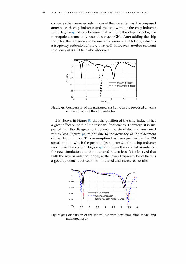
98 electrically small antenna design using chip inductor
compares the measured return loss of the two antennas: the proposedantenna with chip inductor and the one without the chip inductor.From Figure 91, it can be seen that without the chip inductor, themonopole antenna only resonates at 4.15 GHz. After adding the chipinductor, this antenna can be made to resonate at 2.6 GHz, which isa frequency reduction of more than 37%. Moreover, another resonantfrequency at 5.2 GHz is also observed.
2 3 4 5 6 7−30
−25
−20
−15
−10
−5
0
Freq(GHz)
S11
(dB
)
ant with inductorant without inductor
Figure 91: Comparison of the measured S11 between the proposed antennawith and without the chip inductor
It is shown in Figure 89 that the position of the chip inductor hasa great effect on both of the resonant frequencies. Therefore, it is sus-pected that the disagreement between the simulated and measuredreturn loss (Figure 90) might due to the accuracy of the placementof the chip inductor. This assumption has been justified by the EMsimulation, in which the position (parameter d) of the chip inductorwas moved by 0.5mm. Figure 92 compares the original simulation,the new simulation and the measured return loss. It is observed thatwith the new simulation model, at the lower frequency band there isa good agreement between the simulated and measured results.
2 2.5 3 3.5 4 4.5 5 5.5 6−30
−25
−20
−15
−10
−5
0
MeasurementOriginalSimulation New simulation with d+0.5mm
Figure 92: Comparison of the return loss with new simulation model andmeasured result
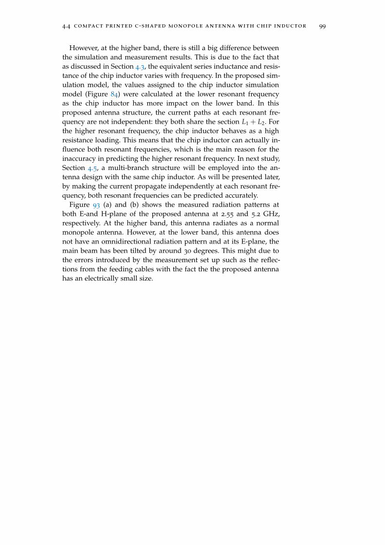
4.4 compact printed c-shaped monopole antenna with chip inductor 99
However, at the higher band, there is still a big difference betweenthe simulation and measurement results. This is due to the fact thatas discussed in Section 4.3, the equivalent series inductance and resis-tance of the chip inductor varies with frequency. In the proposed sim-ulation model, the values assigned to the chip inductor simulationmodel (Figure 84) were calculated at the lower resonant frequencyas the chip inductor has more impact on the lower band. In thisproposed antenna structure, the current paths at each resonant fre-quency are not independent: they both share the section L1 + L2. Forthe higher resonant frequency, the chip inductor behaves as a highresistance loading. This means that the chip inductor can actually in-fluence both resonant frequencies, which is the main reason for theinaccuracy in predicting the higher resonant frequency. In next study,Section 4.5, a multi-branch structure will be employed into the an-tenna design with the same chip inductor. As will be presented later,by making the current propagate independently at each resonant fre-quency, both resonant frequencies can be predicted accurately.
Figure 93 (a) and (b) shows the measured radiation patterns atboth E-and H-plane of the proposed antenna at 2.55 and 5.2 GHz,respectively. At the higher band, this antenna radiates as a normalmonopole antenna. However, at the lower band, this antenna doesnot have an omnidirectional radiation pattern and at its E-plane, themain beam has been tilted by around 30 degrees. This might due tothe errors introduced by the measurement set up such as the reflec-tions from the feeding cables with the fact the the proposed antennahas an electrically small size.
100 electrically small antenna design using chip inductor
0°15°30°
45°
60°
75°
90°
105 °
120 °
135 °
150 °165 °±180 °−165°
−150°
−135°
−120°
−105°
−90°
−75°
−60°
−45°
−30°−15°
−20
−10
0
(a)
0°15°30°
45°
60°
75°
90°
105 °
120 °
135 °
150 °165 °±180 °−165°
−150°
−135°
−120°
−105°
−90°
−75°
−60°
−45°
−30°−15°
−20
−10
0
(b)
Figure 93: Measured radiation pattern at X-Y plane (solid line) and X-Zplane (dashed line) at (a) 2.55GHz and (b) 5.25GHz
Figure 94 (a) and (b) shows the simulated peak gain of the an-tenna at its lower and higher band, respectively. The simulation re-sults show that the peak gain of the proposed antenna at 2.55 GHzis 2.2 dB while the peak gain at 5.25 GHz is 4.7 dB. From the simula-tion results, it is also found that the radiation efficiency at both bandsis around 90% whilst the radiation efficiency of the antenna withoutthe chip inductor is 98% at its resonant frequency. This means that in-troducing the chip inductor does not greatly influence the radiationefficiency of the original antenna.
Table 3 shows the calculated quality factor (Q) of the proposedantenna and its theoretical Q lower bound by using the equationssuggested in Section 4.2. In this calculation, the frequency range wasdefined by the standard of VSWR 3:1. From Table 3, it can be seen thatthe proposed antenna has ka smaller than 0.5, which means that theantenna has an electrically small size. Compared to its Q factor lowerbound calculated using Equation 99, the proposed antenna exhibits aquality factor close to it.
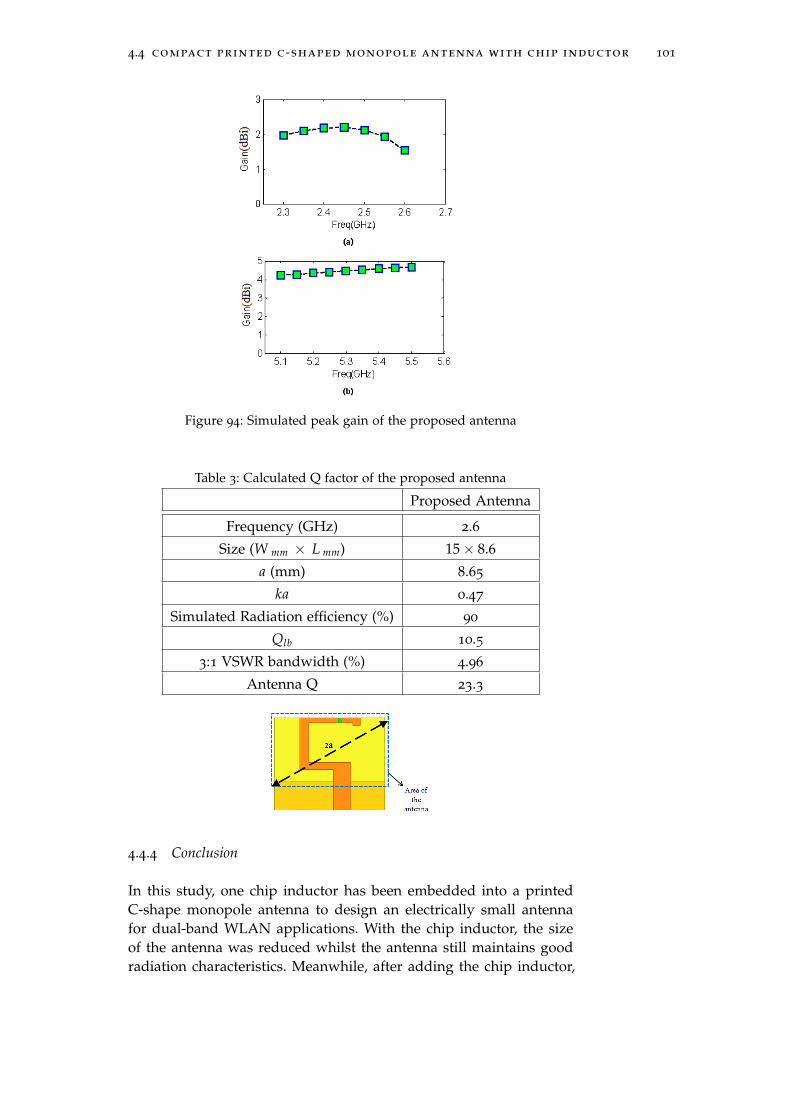
4.4 compact printed c-shaped monopole antenna with chip inductor 101
Figure 94: Simulated peak gain of the proposed antenna
Table 3: Calculated Q factor of the proposed antenna
Proposed Antenna
Frequency (GHz) 2.6
Size (W mm × L mm) 15× 8.6
a (mm) 8.65
ka 0.47
Simulated Radiation efficiency (%) 90
Qlb 10.5
3:1 VSWR bandwidth (%) 4.96
Antenna Q 23.3
4.4.4 Conclusion
In this study, one chip inductor has been embedded into a printedC-shape monopole antenna to design an electrically small antennafor dual-band WLAN applications. With the chip inductor, the sizeof the antenna was reduced whilst the antenna still maintains goodradiation characteristics. Meanwhile, after adding the chip inductor,
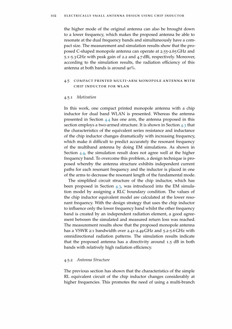
102 electrically small antenna design using chip inductor
the higher mode of the original antenna can also be brought downto a lower frequency, which makes the proposed antenna be able toresonate at the dual frequency bands and simultaneously have a com-pact size. The measurement and simulation results show that the pro-posed C-shaped monopole antenna can operate at 2.55-2.65 GHz and5.1-5.3 GHz with peak gain of 2.2 and 4.7 dBi, respectively. Moreover,according to the simulation results, the radiation efficiency of thisantenna at both bands is around 90%.
4.5 compact printed multi-arm monopole antenna with
chip inductor for wlan
4.5.1 Motivation
In this work, one compact printed monopole antenna with a chipinductor for dual band WLAN is presented. Whereas the antennapresented in Section 4.4 has one arm, the antenna proposed in thissection employs a two-armed structure. It is shown in Section 4.3 thatthe characteristics of the equivalent series resistance and inductanceof the chip inductor changes dramatically with increasing frequency,which make it difficult to predict accurately the resonant frequencyof the multiband antenna by doing EM simulations. As shown inSection 4.4, the simulation result does not agree well at the higherfrequency band. To overcome this problem, a design technique is pro-posed whereby the antenna structure exhibits independent currentpaths for each resonant frequency and the inductor is placed in oneof the arms to decrease the resonant length of the fundamental mode.
The simplified circuit structure of the chip inductor, which hasbeen proposed in Section 4.3, was introduced into the EM simula-tion model by assigning a RLC boundary condition. The values ofthe chip inductor equivalent model are calculated at the lower reso-nant frequency. With the design strategy that uses the chip inductorto influence only the lower frequency band whilst the other frequencyband is created by an independent radiation element, a good agree-ment between the simulated and measured return loss was reached.The measurement results show that the proposed monopole antennahas a VSWR 2:1 bandwidth over 2.41-2.49 GHz and 5.2-5.6 GHz withomnidirectional radiation patterns. The simulation results indicatethat the proposed antenna has a directivity around 1.5 dB in bothbands with relatively high radiation efficiency.
4.5.2 Antenna Structure
The previous section has shown that the characteristics of the simpleRL equivalent circuit of the chip inductor changes considerably athigher frequencies. This promotes the need of using a multi-branch
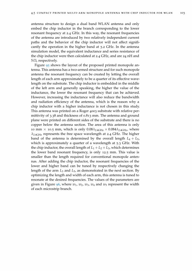
4.5 compact printed multi-arm monopole antenna with chip inductor for wlan 103
antenna structure to design a dual band WLAN antenna and onlyembed the chip inductor in the branch corresponding to the lowerresonant frequency at 2.4 GHz. In this way, the resonant frequenciesof the antenna are introduced by two relatively independent currentpaths and the behavior of the chip inductor will not affect signifi-cantly the operation in the higher band at 5.2 GHz. In the antennasimulation model, the equivalent inductance and series resistance ofthe chip inductor were then calculated at 2.4 GHz, and are 24 nH and5 Ω, respectively.
Figure 95 shows the layout of the proposed printed monopole an-tenna. This antenna has a two-armed structure and for such monopoleantenna the resonant frequency can be created by letting the overalllength of each arm approximately to be a quarter of its effective wave-length on the substrate. The chip inductor is embedded in the middleof the left arm and generally speaking, the higher the value of theinductance, the lower the resonant frequency that can be achieved.However, increasing the inductance will also reduce the bandwidthand radiation efficiency of the antenna, which is the reason why achip inductor with a higher inductance is not chosen in this study.This antenna was printed on a Roger 4003 substrate with relative per-mittivity of 3.38 and thickness of 0.813 mm. The antenna and groundplane were printed on different sides of the substrate and there is nocopper below the antenna section. The area of this antenna is only10 mm × 10.5 mm, which is only 0.08λ2.4GHz × 0.084λ2.4GHz, whereλ2.4GHz represents the free space wavelength at 2.4 GHz. The higherband of the antenna is determined by the overall length L4 + L5,which is approximately a quarter of a wavelength at 5.3 GHz. Withthe chip inductor, the overall length of L1 + L2 + L3, which determinesthe lower band resonant frequency, is only 12.5 mm. This value issmaller than the length required for conventional monopole anten-nas. After adding the chip inductor, the resonant frequencies of thelower and higher band can be tuned by respectively changing thelength of the arm L3 and L5, as demonstrated in the next section. Byoptimizing the length and width of each arm, this antenna is tuned toresonate at the desired frequencies. The values of the parameters aregiven in Figure 96, where w1, w2, w3, w4 and w5 represent the widthof each microstrip branch.
104 electrically small antenna design using chip inductor
Figure 95: The top view of the proposed multi-arm monopole antenna
Figure 96: Detailed view of the antenna radiation element with dimensions
4.5.3 Simulated and Measured Results
The proposed two-armed monopole antenna was fabricated and thereturn loss was measured using Agilent PNA E8363B. Figure 97 presentsthe comparison between the simulated and measured return loss ofthe antenna. The dashed line represents the simulation results of us-ing the proposed simulation model of the inductor whereas the re-sults based on a simple inductor of nominal value equal to 20 nH arerepresented by the dotted line. It can be seen that the use of a simpleinductor model fails to predict accurately the operation frequency ofthe antenna. Using the proposed method, there is a good agreementbetween the measurement and simulation results of the return lossexcept for the amplitude of the S11 at the higher band. This is dueto the fact that in the simulation model, the values of the equivalentseries inductance and resistance are chosen at 2.4 GHz. At higherresonant frequency, as shown in Figure 81, the chip inductor acts asa high impedance resistor, which influences the real part of the in-put impedance of the antenna and as a consequence, the impedance
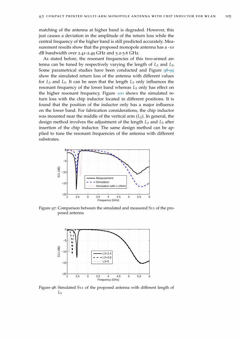
4.5 compact printed multi-arm monopole antenna with chip inductor for wlan 105
matching of the antenna at higher band is degraded. However, thisjust causes a deviation in the amplitude of the return loss while thecentral frequency of the higher band is still predicted accurately. Mea-surement results show that the proposed monopole antenna has a -10
dB bandwidth over 2.41-2.49 GHz and 5.2-5.6 GHz.As stated before, the resonant frequencies of this two-armed an-
tenna can be tuned by respectively varying the length of L3 and L5.Some parametrical studies have been conducted and Figure 98-99
show the simulated return loss of the antenna with different valuesfor L3 and L5. It can be seen that the length L3 only influences theresonant frequency of the lower band whereas L5 only has effect onthe higher resonant frequency. Figure 100 shows the simulated re-turn loss with the chip inductor located in different positions. It isfound that the position of the inductor only has a major influenceon the lower band. For fabrication considerations, the chip inductorwas mounted near the middle of the vertical arm (L2). In general, thedesign method involves the adjustment of the length L3 and L5 afterinsertion of the chip inductor. The same design method can be ap-plied to tune the resonant frequencies of the antenna with differentsubstrates.
2 2.5 3 3.5 4 4.5 5 5.5 6−20
−15
−10
−5
00
Frequency (GHz)
S11
(dB
)
MeasurementSimulationSimulation with L=20nH
Figure 97: Comparison between the simulated and measured S11 of the pro-posed antenna
2 2.5 3 3.5 4 4.5 5 5.5 6−20
−15
−10
−5
0
Frequency (GHz)
S11
(dB
)
L3=2.4L3=3.8L3=5
Figure 98: Simulated S11 of the proposed antenna with different length ofL3
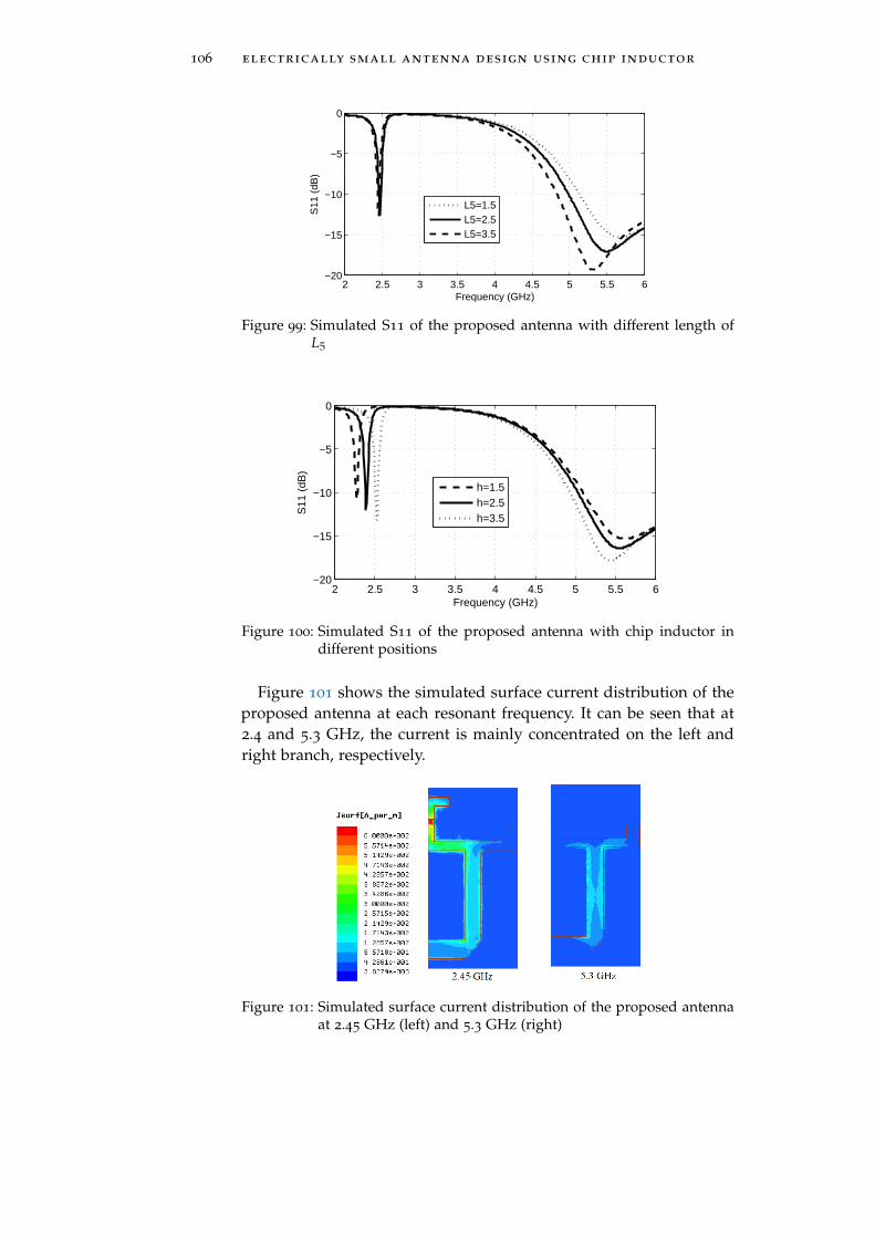
106 electrically small antenna design using chip inductor
2 2.5 3 3.5 4 4.5 5 5.5 6−20
−15
−10
−5
0
Frequency (GHz)
S11
(dB
)
L5=1.5L5=2.5L5=3.5
Figure 99: Simulated S11 of the proposed antenna with different length ofL5
2 2.5 3 3.5 4 4.5 5 5.5 6−20
−15
−10
−5
0
Frequency (GHz)
S11
(dB
)
h=1.5h=2.5h=3.5
Figure 100: Simulated S11 of the proposed antenna with chip inductor indifferent positions
Figure 101 shows the simulated surface current distribution of theproposed antenna at each resonant frequency. It can be seen that at2.4 and 5.3 GHz, the current is mainly concentrated on the left andright branch, respectively.
Figure 101: Simulated surface current distribution of the proposed antennaat 2.45 GHz (left) and 5.3 GHz (right)
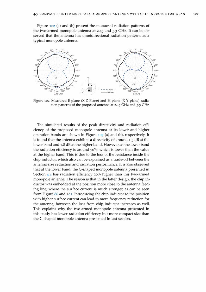
4.5 compact printed multi-arm monopole antenna with chip inductor for wlan 107
Figure 102 (a) and (b) present the measured radiation patterns ofthe two-armed monopole antenna at 2.45 and 5.3 GHz. It can be ob-served that the antenna has omnidirectional radiation patterns as atypical monopole antenna.
0°15°
30°
45°
60°
75°
90°
105 °
120 °
135 °
150 °
165 °±180 ° −165°
−150°
−135°
−120°
−105°
−90°
−75°
−60°
−45°
−30°
−15°
−20
−10
0
2.45 GHz
0°15°
30°
45°
60°
75°
90°
105 °
120 °
135 °
150 °
165 °±180 ° −165°
−150°
−135°
−120°
−105°
−90°
−75°
−60°
−45°
−30°
−15°
−20
−10
0
E Plane
H Plane5.3 GHz
Figure 102: Measured E-plane (X-Z Plane) and H-plane (X-Y plane) radia-tion patterns of the proposed antenna at 2.45 GHz and 5.3 GHz
The simulated results of the peak directivity and radiation effi-ciency of the proposed monopole antenna at its lower and higheroperation bands are shown in Figure 103 (a) and (b), respectively. Itis found that the antenna exhibits a directivity of around 1.5 dB at thelower band and 1.8 dB at the higher band. However, at the lower bandthe radiation efficiency is around 70%, which is lower than the valueat the higher band. This is due to the loss of the resistance inside thechip inductor, which also can be explained as a trade-off between theantenna size reduction and radiation performance. It is also observedthat at the lower band, the C-shaped monopole antenna presented inSection 4.4 has radiation efficiency 20% higher than this two-armedmonopole antenna. The reason is that in the latter design, the chip in-ductor was embedded at the position more close to the antenna feed-ing line, where the surface current is much stronger, as can be seenfrom Figure 86 and 101. Introducing the chip inductor to the positionwith higher surface current can lead to more frequency reduction forthe antenna; however, the loss from chip inductor increases as well.This explains why the two-armed monopole antenna presented inthis study has lower radiation efficiency but more compact size thanthe C-shaped monopole antenna presented in last section.
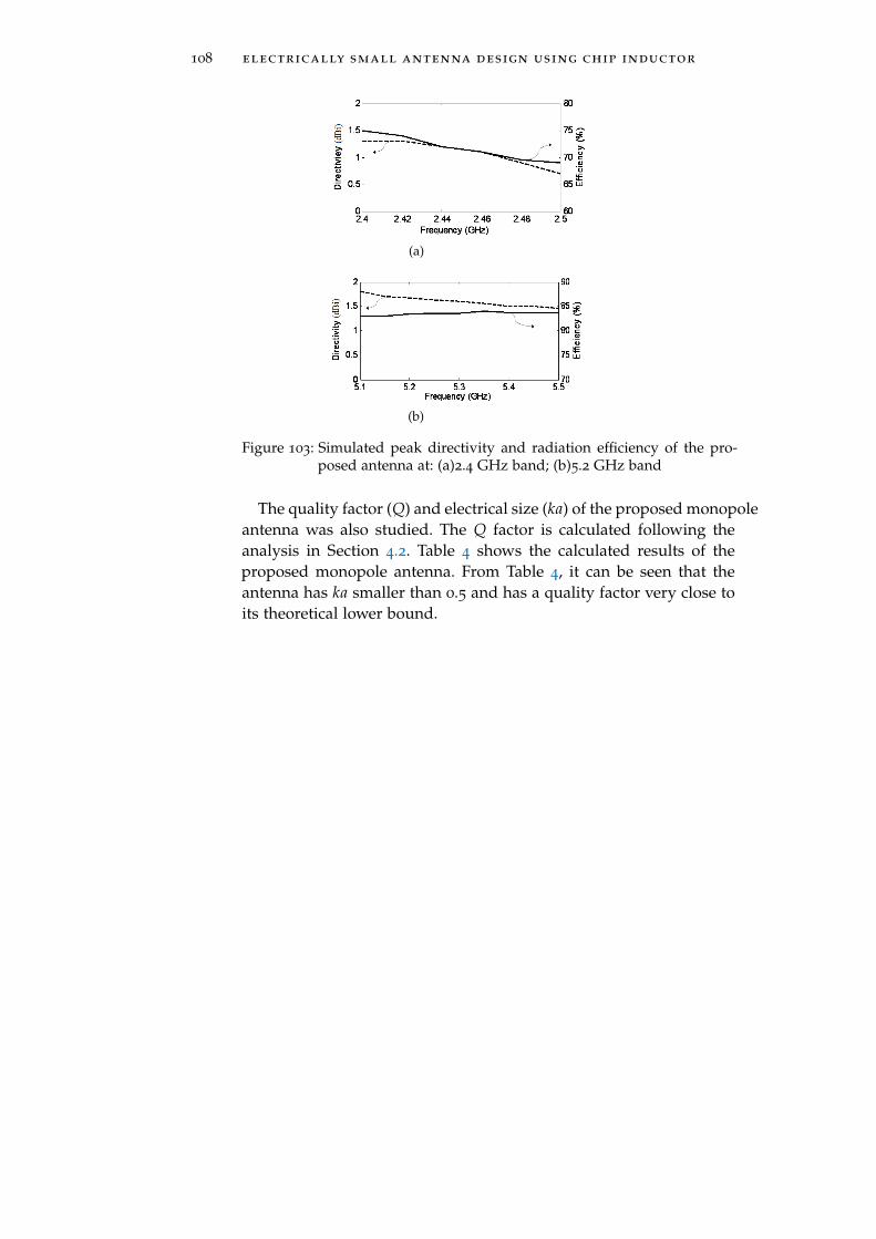
108 electrically small antenna design using chip inductor
(a)
(b)
Figure 103: Simulated peak directivity and radiation efficiency of the pro-posed antenna at: (a)2.4 GHz band; (b)5.2 GHz band
The quality factor (Q) and electrical size (ka) of the proposed monopoleantenna was also studied. The Q factor is calculated following theanalysis in Section 4.2. Table 4 shows the calculated results of theproposed monopole antenna. From Table 4, it can be seen that theantenna has ka smaller than 0.5 and has a quality factor very close toits theoretical lower bound.
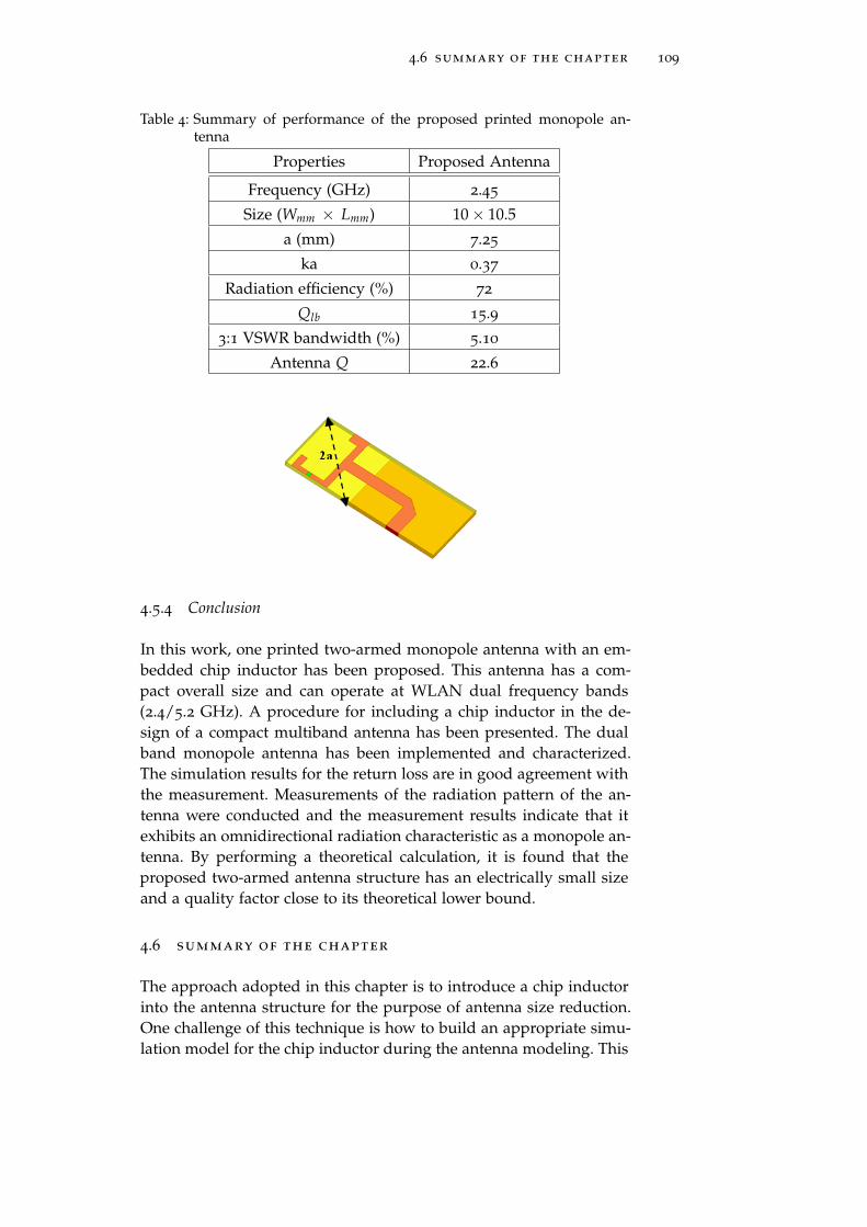
4.6 summary of the chapter 109
Table 4: Summary of performance of the proposed printed monopole an-tenna
Properties Proposed Antenna
Frequency (GHz) 2.45
Size (Wmm × Lmm) 10× 10.5
a (mm) 7.25
ka 0.37
Radiation efficiency (%) 72
Qlb 15.9
3:1 VSWR bandwidth (%) 5.10
Antenna Q 22.6
4.5.4 Conclusion
In this work, one printed two-armed monopole antenna with an em-bedded chip inductor has been proposed. This antenna has a com-pact overall size and can operate at WLAN dual frequency bands(2.4/5.2 GHz). A procedure for including a chip inductor in the de-sign of a compact multiband antenna has been presented. The dualband monopole antenna has been implemented and characterized.The simulation results for the return loss are in good agreement withthe measurement. Measurements of the radiation pattern of the an-tenna were conducted and the measurement results indicate that itexhibits an omnidirectional radiation characteristic as a monopole an-tenna. By performing a theoretical calculation, it is found that theproposed two-armed antenna structure has an electrically small sizeand a quality factor close to its theoretical lower bound.
4.6 summary of the chapter
The approach adopted in this chapter is to introduce a chip inductorinto the antenna structure for the purpose of antenna size reduction.One challenge of this technique is how to build an appropriate simu-lation model for the chip inductor during the antenna modeling. This

110 electrically small antenna design using chip inductor
issue has been solved by investigating the equivalent circuit structureof the chip inductor and simplifying it into a series circuit structurewith only one series inductor and series resistor. Based on this study,a design procedure of how to introduce the chip inductor to designa multiband antenna has been proposed. Then, two electrically smallantennas for dual band WLAN applications are presented. It is im-portant to point out that although greatly size reduction has beenachieved, but there is some reduction in the antenna bandwidth aswell as the radiation efficiency especially at the lower resonant fre-quencies. The following is the list of publications resulted from thework presented in this chapter:
1. Qi Luo; J. R. Pereira and H.M. Salgado. Compact printed monopoleantenna with chip inductor for WLAN. IEEE Antennas and Wire-less Propagation Letters, 10:880-883, September 2011.
2. Qi Luo; Jose Pereira and Henrique Salgado. Compact PrintedC-shaped Monopole Antenna With Chip Inductor. In Proceed-ings of IEEE International Symposium on Antennas and Propagation,Washington, USA, July 2011.
5P R I N T E D M O N O P O L E A N T E N N A F O R M U LT I B A N DM O B I L E P H O N E A P P L I C AT I O N S
5.1 introduction
After successfully applying the chip inductor to design two electri-cally small antennas for dual band WLAN applications and given theneed for multiband operation of current mobile devices, it is decidedto further investigate this technique to design a compact multibandprinted monopole antenna that can operate at multiple frequencybands for a mobile handset.
This chapter is organized as follows. Section 5.2 presents the mo-tivation of this work and the structure of the proposed multibandmonopole antenna is depicted in Section 5.3. Then, Section 5.4 presentsboth the simulated and measured results of the antenna including thereturn loss and radiation patterns. In this section, the radiation per-formances of the antenna when it is placed in the plastic housing orwith ground planes of different lengths have also been investigated.The radiation performance and the SAR level of the antenna when itis placed in close proximity to the human head are studied in Section5.5. A brief summary of this chapter is presented in Section 5.6.
5.2 motivation
The rapid growth in mobile communications increases the needs ofdesigning multiband internal antennas for mobile terminals. Mean-while, it is also desirable to design such antennas as compact as pos-sible. Planar Invert-F Antenna (PIFA) is one type of conventional an-tennas that has been widely employed in mobile phones. In [77, 78],two coupled-fed compact multiband PIFAs for wireless wide area net-works (WWAN) were proposed for internal mobile phone antennaapplications. The size reduction of these two antennas was achievedby shorting the antenna to the ground and bending the antenna struc-ture. Printed monopole slot antennas and printed loop antennas havealso been widely studied for multiband internal mobile phones. In[79, 80], two folded monopole slot antennas that can cover the penta-band WWAN operation were proposed for clam-shell mobile phones.These two antennas were designed by making several slots on thetop of the ground plane. In [81, 82, 83], printed half-wavelength andmeandered loop antenna were proposed for the design of multibandantenna for mobile handsets. However, all of these antennas have
111

112 printed monopole antenna for multiband mobile phone applications
operating bands only covering GSM850/900 and DCS/PCS/UMTSbands, which not enough for nowadays wireless communications.
To make the antenna resonant at additional bands including Wire-less LAN, one novel PIFA structure combining shorted parasitic patches,capacitive loads and slots was designed to support both quad-bandmobile communication and dual-band wireless local area network(WLAN) operations [84]. Although this antenna can operate at severalbands, it is extremely difficult to fabricate due to its complex struc-ture. In [85], multiband operation including the WWAN and WLAN2.4 GHz was achieved by cutting slots of different lengths at the edgeof the system ground plane of the mobile phone. An even more opera-tion bands including GSM/DCS/PCS/UMTS/WLAN/WiMAX wereachieved by cutting the loop-like slot on the top of the ground planeand shorting it to the ground plane [86]. However, shorting the an-tenna to the ground makes the resonant frequencies of the antennavulnerable to the length of the ground plane and the ground planesize used in [86] is smaller than the size of the system ground planefor a mobile phone. Other techniques have also been developed to de-sign compact multiband antennas for wireless communications. In[87], a multiband antenna that can support WWAN and 2.4 GHzWLAN frequency bands was realized by using a switchable feed andground. In [88], a small size multiband antenna for wireless mobilesystem is designed based on double negative (DNG) zeroth order res-onator (ZOR). However, it is noticed that these antennas have rathercomplex structures and they are quite difficult to fabricate. In [13],a chip inductor was embedded in the printed monopole antenna,which resulted in a compact antenna for mobile handset application.
In this work, it aims to continue the studies presented in last chap-ter and implement the chip inductor technique to design a multi-frequency antenna that can cover most of the required frequencybands for mobile communications. Meanwhile, the antenna proposedhas a planar structure and is easy to fabricate, which overcomes mostof the shortcomings of previous designs.
5.3 antenna structure
Having in mind the limitations of the antennas developed and re-ported in previous work, this study aims to explore further multi-band monopole antennas design with low complexity and suitablefor mobile phone applications. From the work presented in the previ-ous chapter, it is concluded that a multi-branch monopole antenna in-cluding a chip inductor for size reduction would be a feasible method.In this work, an antenna with multi-branch structure and is capableof resonating at five frequencies is presented. Figure 104 shows thestructure of the proposed antenna and the main dimensions of theantenna elements are given in Figure 105. The antenna element is
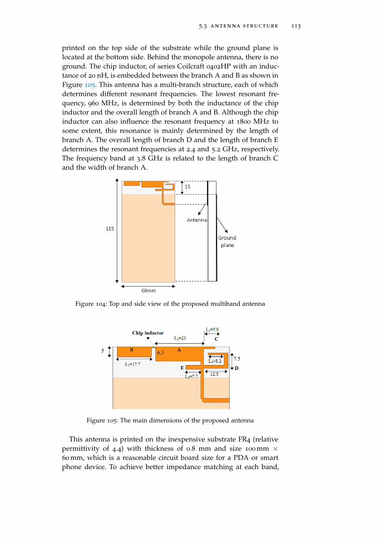
5.3 antenna structure 113
printed on the top side of the substrate while the ground plane islocated at the bottom side. Behind the monopole antenna, there is noground. The chip inductor, of series Coilcraft 0402HP with an induc-tance of 20 nH, is embedded between the branch A and B as shown inFigure 105. This antenna has a multi-branch structure, each of whichdetermines different resonant frequencies. The lowest resonant fre-quency, 960 MHz, is determined by both the inductance of the chipinductor and the overall length of branch A and B. Although the chipinductor can also influence the resonant frequency at 1800 MHz tosome extent, this resonance is mainly determined by the length ofbranch A. The overall length of branch D and the length of branch Edetermines the resonant frequencies at 2.4 and 5.2 GHz, respectively.The frequency band at 3.8 GHz is related to the length of branch Cand the width of branch A.
Figure 104: Top and side view of the proposed multiband antenna
Figure 105: The main dimensions of the proposed antenna
This antenna is printed on the inexpensive substrate FR4 (relativepermittivity of 4.4) with thickness of 0.8 mm and size 100 mm ×60 mm, which is a reasonable circuit board size for a PDA or smartphone device. To achieve better impedance matching at each band,
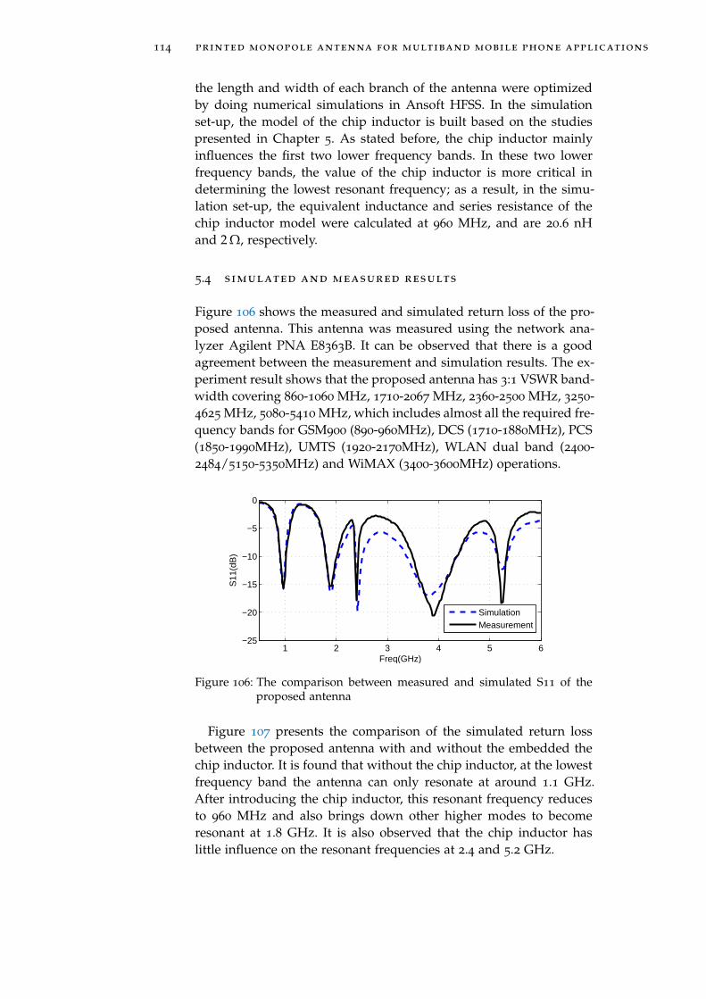
114 printed monopole antenna for multiband mobile phone applications
the length and width of each branch of the antenna were optimizedby doing numerical simulations in Ansoft HFSS. In the simulationset-up, the model of the chip inductor is built based on the studiespresented in Chapter 5. As stated before, the chip inductor mainlyinfluences the first two lower frequency bands. In these two lowerfrequency bands, the value of the chip inductor is more critical indetermining the lowest resonant frequency; as a result, in the simu-lation set-up, the equivalent inductance and series resistance of thechip inductor model were calculated at 960 MHz, and are 20.6 nHand 2 Ω, respectively.
5.4 simulated and measured results
Figure 106 shows the measured and simulated return loss of the pro-posed antenna. This antenna was measured using the network ana-lyzer Agilent PNA E8363B. It can be observed that there is a goodagreement between the measurement and simulation results. The ex-periment result shows that the proposed antenna has 3:1 VSWR band-width covering 860-1060 MHz, 1710-2067 MHz, 2360-2500 MHz, 3250-4625 MHz, 5080-5410 MHz, which includes almost all the required fre-quency bands for GSM900 (890-960MHz), DCS (1710-1880MHz), PCS(1850-1990MHz), UMTS (1920-2170MHz), WLAN dual band (2400-2484/5150-5350MHz) and WiMAX (3400-3600MHz) operations.
1 2 3 4 5 6−25
−20
−15
−10
−5
0
Freq(GHz)
S11
(dB
)
SimulationMeasurement
Figure 106: The comparison between measured and simulated S11 of theproposed antenna
Figure 107 presents the comparison of the simulated return lossbetween the proposed antenna with and without the embedded thechip inductor. It is found that without the chip inductor, at the lowestfrequency band the antenna can only resonate at around 1.1 GHz.After introducing the chip inductor, this resonant frequency reducesto 960 MHz and also brings down other higher modes to becomeresonant at 1.8 GHz. It is also observed that the chip inductor haslittle influence on the resonant frequencies at 2.4 and 5.2 GHz.
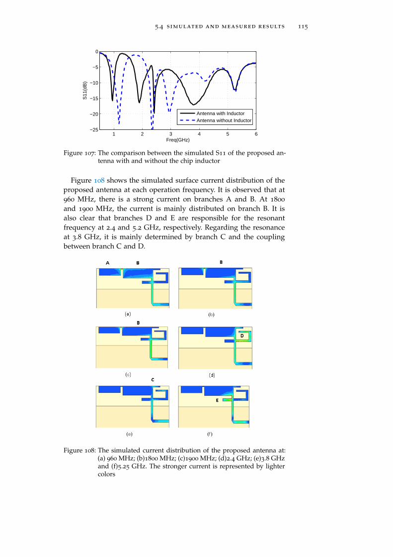
5.4 simulated and measured results 115
1 2 3 4 5 6−25
−20
−15
−10
−5
0
Freq(GHz)
S11
(dB
)
Antenna with InductorAntenna without Inductor
Figure 107: The comparison between the simulated S11 of the proposed an-tenna with and without the chip inductor
Figure 108 shows the simulated surface current distribution of theproposed antenna at each operation frequency. It is observed that at960 MHz, there is a strong current on branches A and B. At 1800
and 1900 MHz, the current is mainly distributed on branch B. It isalso clear that branches D and E are responsible for the resonantfrequency at 2.4 and 5.2 GHz, respectively. Regarding the resonanceat 3.8 GHz, it is mainly determined by branch C and the couplingbetween branch C and D.
Figure 108: The simulated current distribution of the proposed antenna at:(a) 960 MHz; (b)1800 MHz; (c)1900 MHz; (d)2.4 GHz; (e)3.8 GHzand (f)5.25 GHz. The stronger current is represented by lightercolors
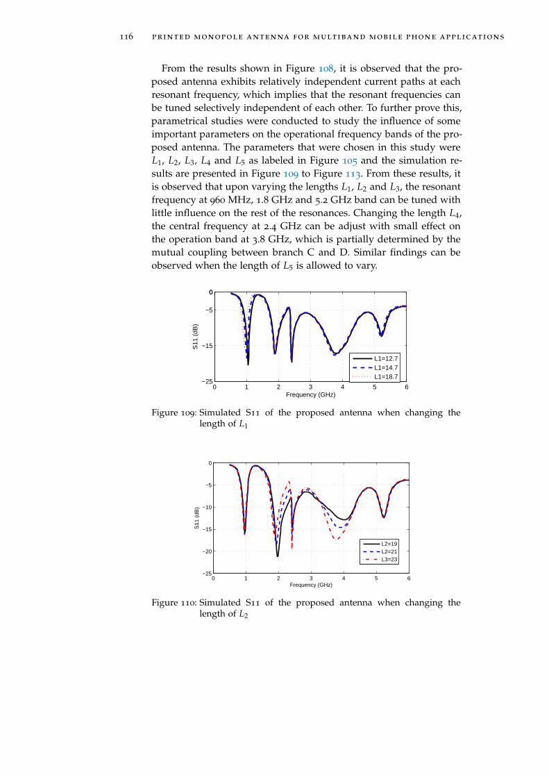
116 printed monopole antenna for multiband mobile phone applications
From the results shown in Figure 108, it is observed that the pro-posed antenna exhibits relatively independent current paths at eachresonant frequency, which implies that the resonant frequencies canbe tuned selectively independent of each other. To further prove this,parametrical studies were conducted to study the influence of someimportant parameters on the operational frequency bands of the pro-posed antenna. The parameters that were chosen in this study wereL1, L2, L3, L4 and L5 as labeled in Figure 105 and the simulation re-sults are presented in Figure 109 to Figure 113. From these results, itis observed that upon varying the lengths L1, L2 and L3, the resonantfrequency at 960 MHz, 1.8 GHz and 5.2 GHz band can be tuned withlittle influence on the rest of the resonances. Changing the length L4,the central frequency at 2.4 GHz can be adjust with small effect onthe operation band at 3.8 GHz, which is partially determined by themutual coupling between branch C and D. Similar findings can beobserved when the length of L5 is allowed to vary.
0 1 2 3 4 5 6−25
−15
−5
00
Frequency (GHz)
S11
(dB
)
L1=12.7L1=14.7L1=18.7
Figure 109: Simulated S11 of the proposed antenna when changing thelength of L1
0 1 2 3 4 5 6−25
−20
−15
−10
−5
0
Frequency (GHz)
S11
(dB
)
L2=19L2=21L3=23
Figure 110: Simulated S11 of the proposed antenna when changing thelength of L2
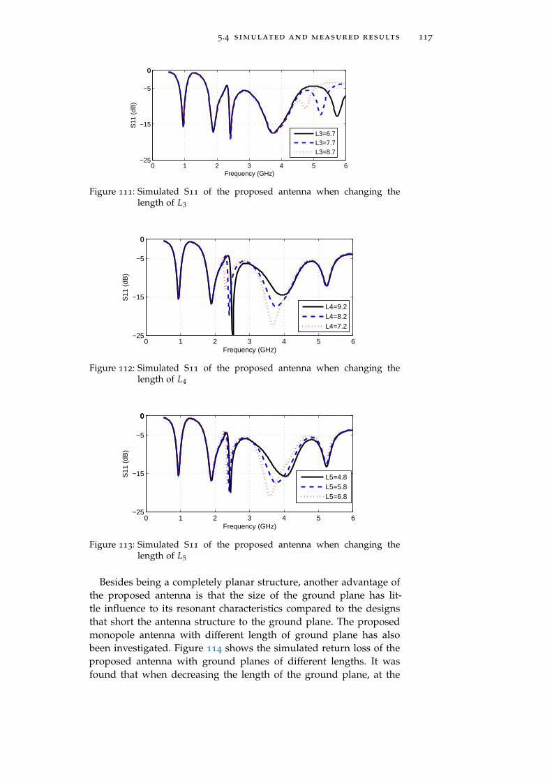
5.4 simulated and measured results 117
0 1 2 3 4 5 6−25
−15
−5
00
Frequency (GHz)
S11
(dB
)
L3=6.7L3=7.7L3=8.7
Figure 111: Simulated S11 of the proposed antenna when changing thelength of L3
0 1 2 3 4 5 6−25
−15
−5
00
Frequency (GHz)
S11
(dB
)
L4=9.2L4=8.2L4=7.2
Figure 112: Simulated S11 of the proposed antenna when changing thelength of L4
0 1 2 3 4 5 6−25
−15
−5
0000
Frequency (GHz)
S11
(dB
)
L5=4.8L5=5.8L5=6.8
Figure 113: Simulated S11 of the proposed antenna when changing thelength of L5
Besides being a completely planar structure, another advantage ofthe proposed antenna is that the size of the ground plane has lit-tle influence to its resonant characteristics compared to the designsthat short the antenna structure to the ground plane. The proposedmonopole antenna with different length of ground plane has alsobeen investigated. Figure 114 shows the simulated return loss of theproposed antenna with ground planes of different lengths. It wasfound that when decreasing the length of the ground plane, at the
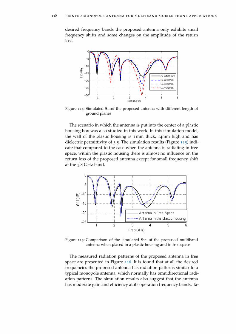
118 printed monopole antenna for multiband mobile phone applications
desired frequency bands the proposed antenna only exhibits smallfrequency shifts and some changes on the amplitude of the returnloss.
1 2 3 4 5 6−30
−25
−20
−15
−10
−5
0
Freq (GHz)
S11
(dB
)
GL=100mmGL=90mmGL=80mmGL=70mm
Figure 114: Simulated S11of the proposed antenna with different length ofground planes
The scenario in which the antenna is put into the center of a plastichousing box was also studied in this work. In this simulation model,the wall of the plastic housing is 1 mm thick, 14mm high and hasdielectric permittivity of 3.5. The simulation results (Figure 115) indi-cate that compared to the case when the antenna is radiating in freespace, within the plastic housing there is almost no influence on thereturn loss of the proposed antenna except for small frequency shiftat the 3.8 GHz band.
Figure 115: Comparison of the simulated S11 of the proposed multibandantenna when placed in a plastic housing and in free space
The measured radiation patterns of the proposed antenna in freespace are presented in Figure 116. It is found that at all the desiredfrequencies the proposed antenna has radiation patterns similar to atypical monopole antenna, which normally has omnidirectional radi-ation patterns. The simulation results also suggest that the antennahas moderate gain and efficiency at its operation frequency bands. Ta-
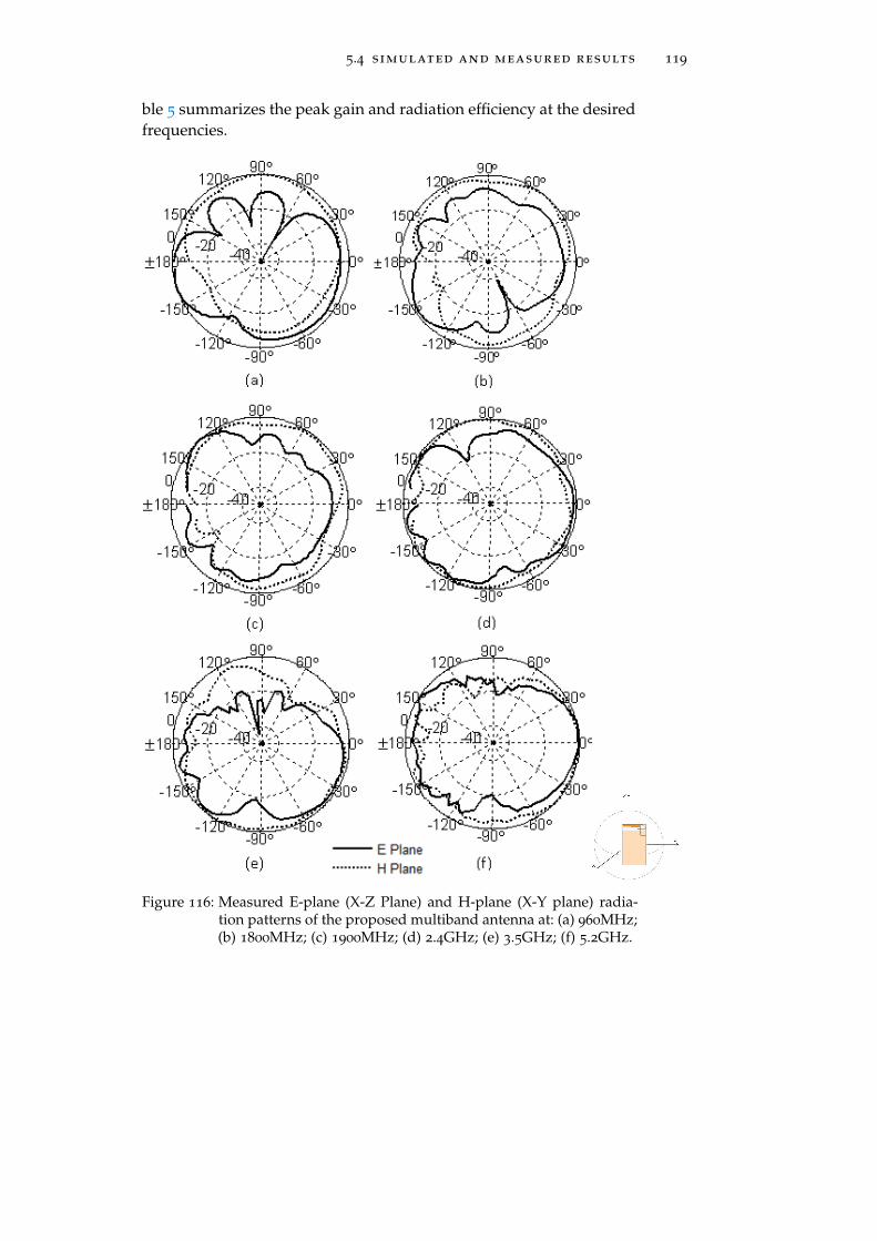
5.4 simulated and measured results 119
ble 5 summarizes the peak gain and radiation efficiency at the desiredfrequencies.
Figure 116: Measured E-plane (X-Z Plane) and H-plane (X-Y plane) radia-tion patterns of the proposed multiband antenna at: (a) 960MHz;(b) 1800MHz; (c) 1900MHz; (d) 2.4GHz; (e) 3.5GHz; (f) 5.2GHz.
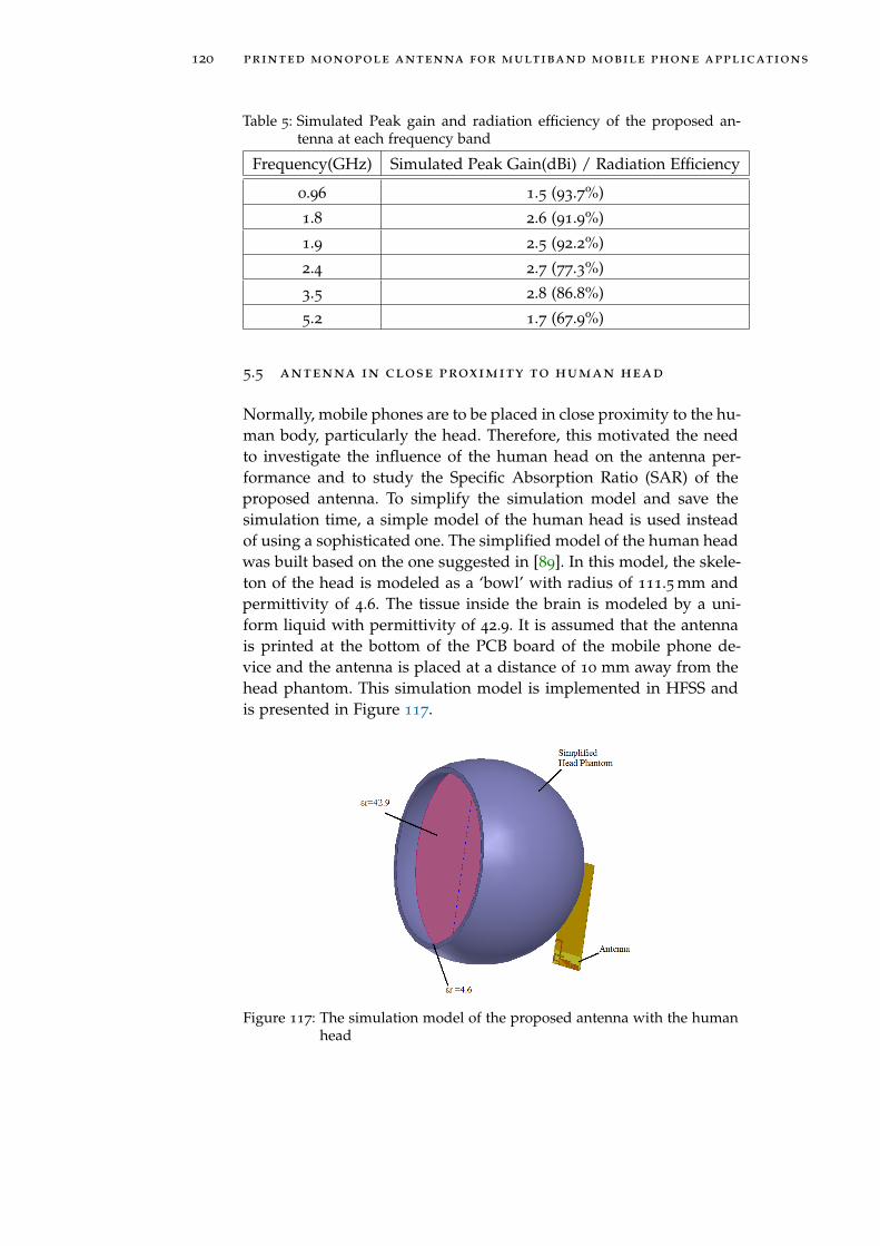
120 printed monopole antenna for multiband mobile phone applications
Table 5: Simulated Peak gain and radiation efficiency of the proposed an-tenna at each frequency band
Frequency(GHz) Simulated Peak Gain(dBi) / Radiation Efficiency
0.96 1.5 (93.7%)
1.8 2.6 (91.9%)
1.9 2.5 (92.2%)
2.4 2.7 (77.3%)
3.5 2.8 (86.8%)
5.2 1.7 (67.9%)
5.5 antenna in close proximity to human head
Normally, mobile phones are to be placed in close proximity to the hu-man body, particularly the head. Therefore, this motivated the needto investigate the influence of the human head on the antenna per-formance and to study the Specific Absorption Ratio (SAR) of theproposed antenna. To simplify the simulation model and save thesimulation time, a simple model of the human head is used insteadof using a sophisticated one. The simplified model of the human headwas built based on the one suggested in [89]. In this model, the skele-ton of the head is modeled as a ‘bowl’ with radius of 111.5 mm andpermittivity of 4.6. The tissue inside the brain is modeled by a uni-form liquid with permittivity of 42.9. It is assumed that the antennais printed at the bottom of the PCB board of the mobile phone de-vice and the antenna is placed at a distance of 10 mm away from thehead phantom. This simulation model is implemented in HFSS andis presented in Figure 117.
Figure 117: The simulation model of the proposed antenna with the humanhead
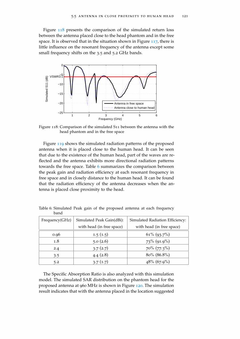
5.5 antenna in close proximity to human head 121
Figure 118 presents the comparison of the simulated return lossbetween the antenna placed close to the head phantom and in the freespace. It is observed that in the situation shown in Figure 117, there islittle influence on the resonant frequency of the antenna except somesmall frequency shifts on the 3.5 and 5.2 GHz bands.
1 2 3 4 5 6−25
−20
−15
−10
−5
0
VSWR3:1
Frequency (GHz)
Sim
ulat
ed S
11 (
dB)
Antenna in free spaceAntenna close to human head
Figure 118: Comparison of the simulated S11 between the antenna with thehead phantom and in the free space
Figure 119 shows the simulated radiation patterns of the proposedantenna when it is placed close to the human head. It can be seenthat due to the existence of the human head, part of the waves are re-flected and the antenna exhibits more directional radiation patternstowards the free space. Table 6 summarizes the comparison betweenthe peak gain and radiation efficiency at each resonant frequency infree space and in closely distance to the human head. It can be foundthat the radiation efficiency of the antenna decreases when the an-tenna is placed close proximity to the head.
Table 6: Simulated Peak gain of the proposed antenna at each frequencyband
Frequency(GHz) Simulated Peak Gain(dBi): Simulated Radiation Efficiency:
with head (in free space) with head (in free space)
0.96 1.5 (1.5) 61% (93.7%)
1.8 5.0 (2.6) 73% (91.9%)
2.4 3.7 (2.7) 70% (77.3%)
3.5 4.4 (2.8) 80% (86.8%)
5.2 3.7 (1.7) 48% (67.9%)
The Specific Absorption Ratio is also analyzed with this simulationmodel. The simulated SAR distribution on the phantom head for theproposed antenna at 960 MHz is shown in Figure 120. The simulationresult indicates that with the antenna placed in the location suggested
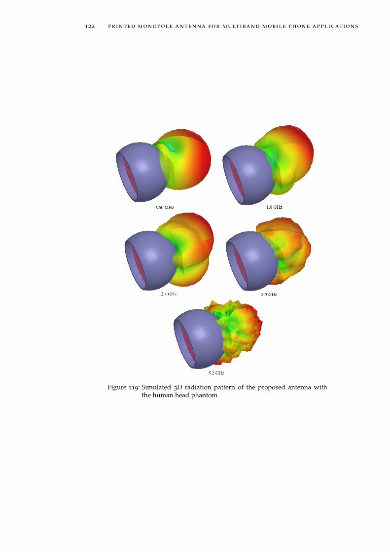
122 printed monopole antenna for multiband mobile phone applications
Figure 119: Simulated 3D radiation pattern of the proposed antenna withthe human head phantom
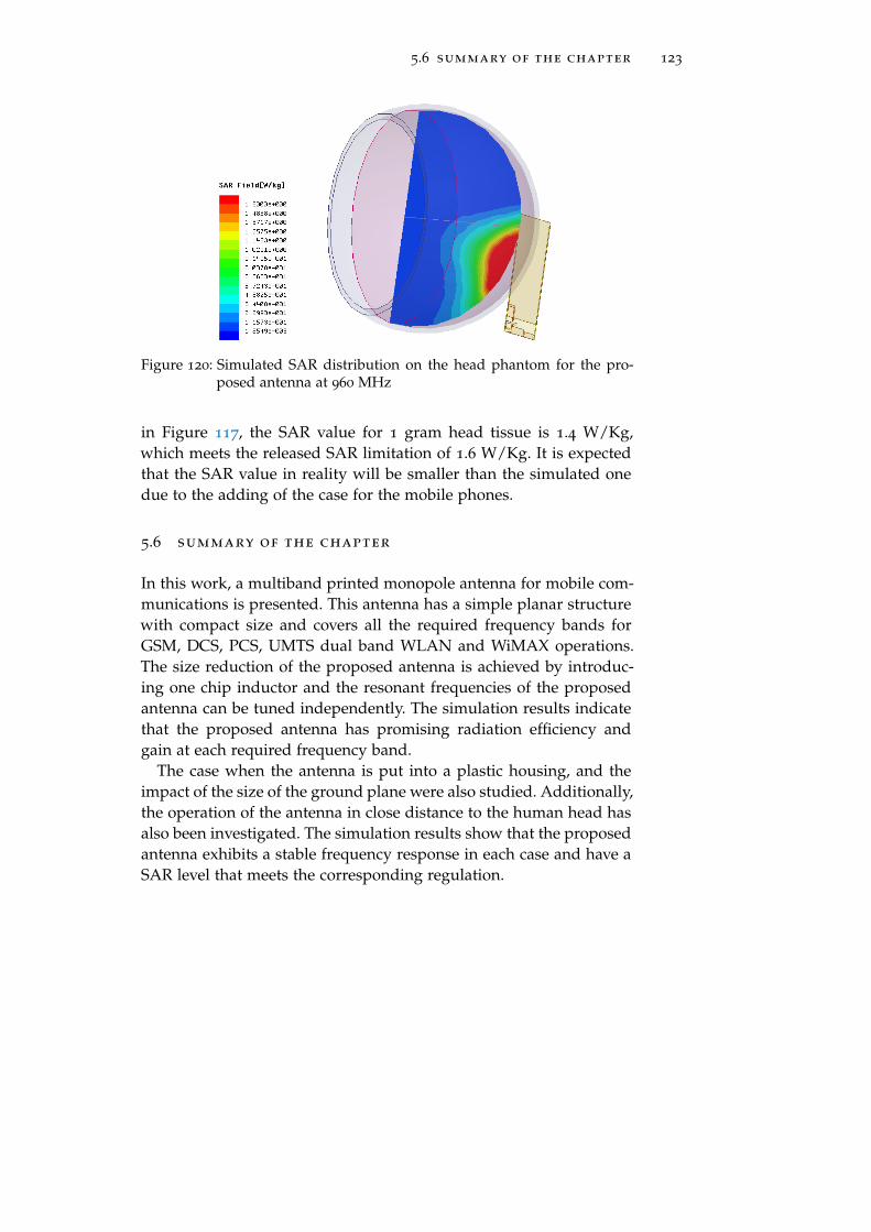
5.6 summary of the chapter 123
Figure 120: Simulated SAR distribution on the head phantom for the pro-posed antenna at 960 MHz
in Figure 117, the SAR value for 1 gram head tissue is 1.4 W/Kg,which meets the released SAR limitation of 1.6 W/Kg. It is expectedthat the SAR value in reality will be smaller than the simulated onedue to the adding of the case for the mobile phones.
5.6 summary of the chapter
In this work, a multiband printed monopole antenna for mobile com-munications is presented. This antenna has a simple planar structurewith compact size and covers all the required frequency bands forGSM, DCS, PCS, UMTS dual band WLAN and WiMAX operations.The size reduction of the proposed antenna is achieved by introduc-ing one chip inductor and the resonant frequencies of the proposedantenna can be tuned independently. The simulation results indicatethat the proposed antenna has promising radiation efficiency andgain at each required frequency band.
The case when the antenna is put into a plastic housing, and theimpact of the size of the ground plane were also studied. Additionally,the operation of the antenna in close distance to the human head hasalso been investigated. The simulation results show that the proposedantenna exhibits a stable frequency response in each case and have aSAR level that meets the corresponding regulation.


6C O M PA C T P R I N T E D M O N O P O L E A N T E N N AA R R AY
6.1 introduction
Multiple-Input-Multiple-Output (MIMO) techniques enable a wire-less device to transmit or receive data with higher data rate. Therecently announced IEEE 802.11n and Long Term Evolution (LTE)standard requires the wireless LAN devices and mobile devices tosupport MIMO. The use of antenna arrays can improve the diver-sity performance of the antenna, which in turn increases the channelcapacity by reducing the fading, suppressing both the random fre-quency modulation and co-channel interference.
The biggest challenge to design a compact antenna array is how tomaintain a good isolation between antennas that are closely spaced.To have good space diversity, traditionally the space between eachantenna elements is required to be approximately half of the wave-length. However, for most of the commercial wireless devices, it isimpossible to follow this rule due to the size constraints. The objec-tive of this chapter is to explore solutions to design compact antennaarrays. The methodology adopted in this study is to employ the ‘neu-tralizing technique’. Before introducing this technique, in Section 6.2,the criterions that are used to evaluate the performance of a MIMOantenna system are introduced. Then, in Section 6.3, one compactinverted-L antenna array for WLAN USB dongle using the neutraliz-ing technique is presented followed by the summary of the chaptergiven in Section 6.4.
6.2 performance analysis of mimo antennas
The performance of a MIMO antenna system can be evaluated bytwo criterions, envelope correlation coefficient and total multi-portreturn loss. The definition of these two concepts as well as a briefmathematical derivation will be introduced in following sections.
6.2.1 Envelope Correlation Coefficient
One important parameter for evaluating the diversity performance ofan antenna array is the envelope correlation coefficient. It is shown in[90] that by modeling the antenna as an open circuit, the correlationcoefficient of two antennas is:
125

126 compact printed monopole antenna array
ρ0jk =E(V0j − V0j)(V0k − V0k)
∗[E(V0j − V0j)2
E[
(V0k − V0k)2]∗]1/2 (109)
with:
V0k(t) =∫∫
Ek(Ω) · h(Ω, t) dΩ (110)
V0j(t) =∫∫
Ej(Ω) · h(Ω, t) dΩ (111)
where j and k is the antenna number, V0k and V0j represent the opencircuit voltage for the k th and j th element, respectively. E is the an-tenna pattern vector, h is the source vector and Ω is the solid angle.The asterisk means complex conjugate and the swung dash repre-sents the time average over the same interval. The envelope correla-tion coefficient ρe is defined as:
ρe ≈ |ρ|2 (112)
Therefore, by integrating the expression given in Equation 109 overthe sphere surround the antennas, the envelope correlation coefficientof a two antenna array can be derived as [91]:
ρe =|∫∫
4π[−→F1 (θ, φ) · −→F2 (θ, φ)]dΩ|2∫∫
4π |−→F1 (θ, φ)|2dΩ ·
∫∫4π |−→F2 (θ, φ)|2dΩ
(113)
where−→Fi (θ, φ) is the field radiation pattern of the antenna system
when antenna i is excited. Generally speaking, the lower the enve-lope correlation coefficient is, the better the diversity of the antennaarray. According to [90], in practical cases the required values of theenvelope correlation coefficient for the base station is ρe<0.7 and forthe mobile devices is ρe<0.5. However, using Formula 113 to calculatethe envelope correlation coefficient, one needs to know the radiationpatterns of the antenna and then solve a complicated integration. Onesimplified solution was proposed in [91], in which it is found that ifthe antennas exhibit high radiation efficiency and the receiving anten-nas are in isotropic signal environments, the envelope correlation canbe approximated by using only the S-parameters instead of comput-ing the radiation patterns of the antenna system:
ρe =|S∗11S12 + S∗21S22|2
(1− (|S11|2 + |S21|2)) · (1− (|S22|2 + |S12|2))(114)
This method has been adopted by many researchers. However, thismethod is based on the assumption that the antennas are lossless.This is not true in a practical situation: there are always losses associ-ated with one antenna such as conduction loss and antenna mismatchloss. In order to refine the method proposed in [91], the radiation ef-

6.2 performance analysis of mimo antennas 127
ficiency has been included in the calculation of the correlation coeffi-cient by taking into account the total radiated powers of the antennas,which can be written as [92]:
Prad,1 = (1− |S11|2 − |S21|2)η1 (115)
Prad,2 = (1− |S22|2 − |S12|2)η2 (116)
where η1 and η2 are the radiation efficiencies of antenna 1 and an-tenna 2. Then, the internal loss of these two antennas can be expressedas:
Ploss,1 = (1− |S11|2 − |S21|2)(1− η1) (117)
Ploss,2 = (1− |S22|2 − |S12|2)(1− η2) (118)
Dividing the total S-matrix into two components, one S-matrix forthe antenna ports and one for the radiation functions, introducing thelosses into the S-matrix and applying the orthogonally requirement,which is a requirement for zero correlation between two columns inan S-matrix, the following expression can be derived:
0 = S11S∗12 + S21S∗22 + ρrec√
Prad,1Prad,2 + ρloss√
Ploss,1Ploss,2 (119)
where ρrec and ρloss are the normalized complex correlation coefficientof the radiation patterns and the internal losses, respectively. Thesetwo terms are defined for the purpose of making them correspondto the generalized S-parameters. Substituting Equation 115 - 118 intoEquation 119 gives:
0 =S11S∗12+S21S∗22
(√
1−|S11|2−|S21|2)(√
1−|S22|2−|S12|2)
+ ρrec√
η1η2 + ρloss
√(1− η1)(1− η2) (120)
Assume that ρloss = 1, which means that the internal loss of theantenna has reached the maximum value and is the worst case, it canbe seen that the following inequality should be satisfied:
S11S∗12 + S21S∗22
(√
1− |S11|2 − |S21|2)(√
1− |S22|2 − |S12|2)η1η2+ ρrec 6
√(
1η1− 1)(
1η2− 1)
(121)Therefore, the maximum and minimum values of the correlation
coefficients can be expressed as:
|ρrec|max,min = |ρrec,0| ±√(
1η1− 1)(
1η2− 1) (122)
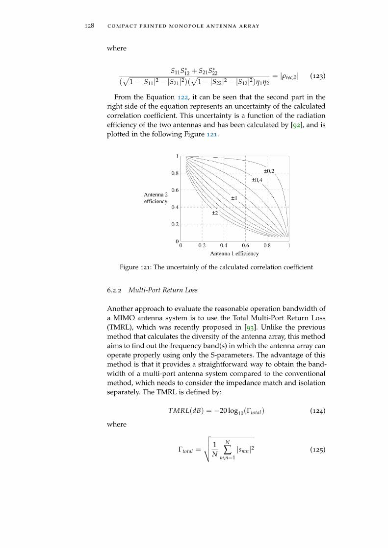
128 compact printed monopole antenna array
where
S11S∗12 + S21S∗22
(√
1− |S11|2 − |S21|2)(√
1− |S22|2 − |S12|2)η1η2= |ρrec,0| (123)
From the Equation 122, it can be seen that the second part in theright side of the equation represents an uncertainty of the calculatedcorrelation coefficient. This uncertainty is a function of the radiationefficiency of the two antennas and has been calculated by [92], and isplotted in the following Figure 121.
Figure 121: The uncertainly of the calculated correlation coefficient
6.2.2 Multi-Port Return Loss
Another approach to evaluate the reasonable operation bandwidth ofa MIMO antenna system is to use the Total Multi-Port Return Loss(TMRL), which was recently proposed in [93]. Unlike the previousmethod that calculates the diversity of the antenna array, this methodaims to find out the frequency band(s) in which the antenna array canoperate properly using only the S-parameters. The advantage of thismethod is that it provides a straightforward way to obtain the band-width of a multi-port antenna system compared to the conventionalmethod, which needs to consider the impedance match and isolationseparately. The TMRL is defined by:
TMRL(dB) = −20 log10(Γtotal) (124)
where
Γtotal =
√√√√ 1N
N
∑m,n=1
|smn|2 (125)
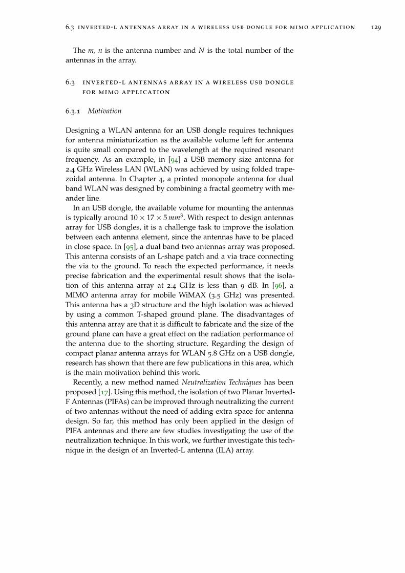
6.3 inverted-l antennas array in a wireless usb dongle for mimo application 129
The m, n is the antenna number and N is the total number of theantennas in the array.
6.3 inverted-l antennas array in a wireless usb dongle
for mimo application
6.3.1 Motivation
Designing a WLAN antenna for an USB dongle requires techniquesfor antenna miniaturization as the available volume left for antennais quite small compared to the wavelength at the required resonantfrequency. As an example, in [94] a USB memory size antenna for2.4 GHz Wireless LAN (WLAN) was achieved by using folded trape-zoidal antenna. In Chapter 4, a printed monopole antenna for dualband WLAN was designed by combining a fractal geometry with me-ander line.
In an USB dongle, the available volume for mounting the antennasis typically around 10× 17× 5 mm3. With respect to design antennasarray for USB dongles, it is a challenge task to improve the isolationbetween each antenna element, since the antennas have to be placedin close space. In [95], a dual band two antennas array was proposed.This antenna consists of an L-shape patch and a via trace connectingthe via to the ground. To reach the expected performance, it needsprecise fabrication and the experimental result shows that the isola-tion of this antenna array at 2.4 GHz is less than 9 dB. In [96], aMIMO antenna array for mobile WiMAX (3.5 GHz) was presented.This antenna has a 3D structure and the high isolation was achievedby using a common T-shaped ground plane. The disadvantages ofthis antenna array are that it is difficult to fabricate and the size of theground plane can have a great effect on the radiation performance ofthe antenna due to the shorting structure. Regarding the design ofcompact planar antenna arrays for WLAN 5.8 GHz on a USB dongle,research has shown that there are few publications in this area, whichis the main motivation behind this work.
Recently, a new method named Neutralization Techniques has beenproposed [17]. Using this method, the isolation of two Planar Inverted-F Antennas (PIFAs) can be improved through neutralizing the currentof two antennas without the need of adding extra space for antennadesign. So far, this method has only been applied in the design ofPIFA antennas and there are few studies investigating the use of theneutralization technique. In this work, we further investigate this tech-nique in the design of an Inverted-L antenna (ILA) array.
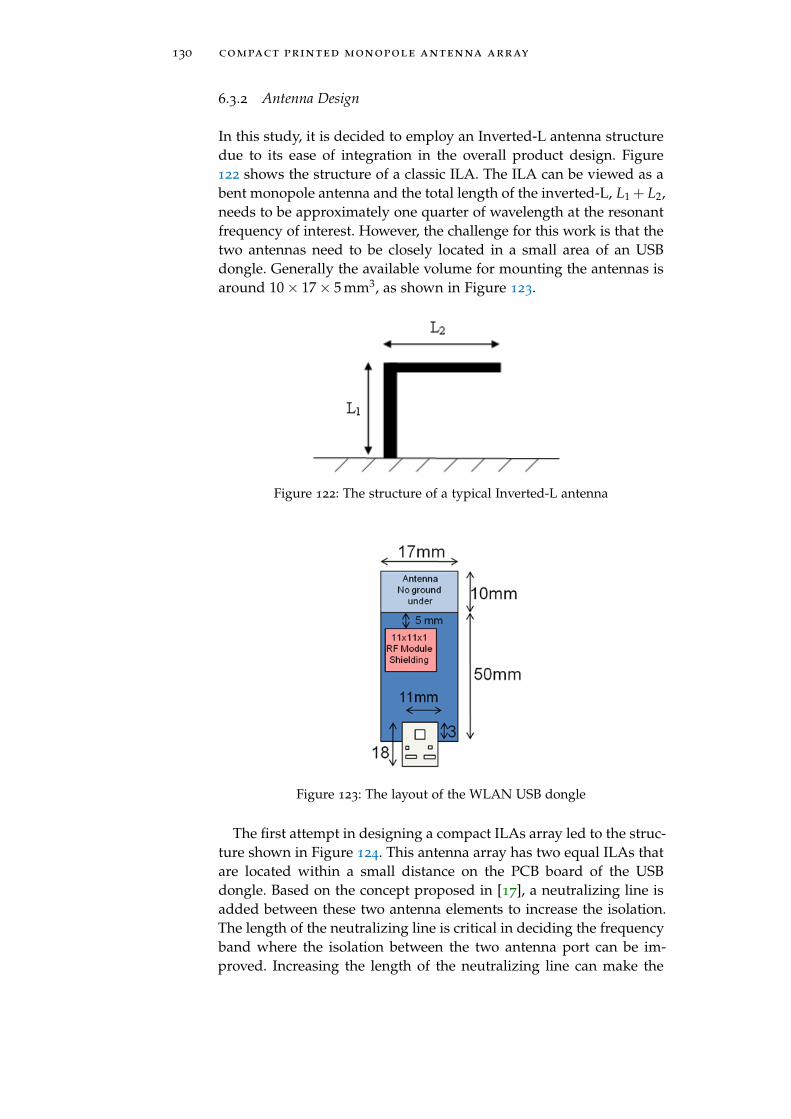
130 compact printed monopole antenna array
6.3.2 Antenna Design
In this study, it is decided to employ an Inverted-L antenna structuredue to its ease of integration in the overall product design. Figure122 shows the structure of a classic ILA. The ILA can be viewed as abent monopole antenna and the total length of the inverted-L, L1 + L2,needs to be approximately one quarter of wavelength at the resonantfrequency of interest. However, the challenge for this work is that thetwo antennas need to be closely located in a small area of an USBdongle. Generally the available volume for mounting the antennas isaround 10× 17× 5 mm3, as shown in Figure 123.
Figure 122: The structure of a typical Inverted-L antenna
Figure 123: The layout of the WLAN USB dongle
The first attempt in designing a compact ILAs array led to the struc-ture shown in Figure 124. This antenna array has two equal ILAs thatare located within a small distance on the PCB board of the USBdongle. Based on the concept proposed in [17], a neutralizing line isadded between these two antenna elements to increase the isolation.The length of the neutralizing line is critical in deciding the frequencyband where the isolation between the two antenna port can be im-proved. Increasing the length of the neutralizing line can make the
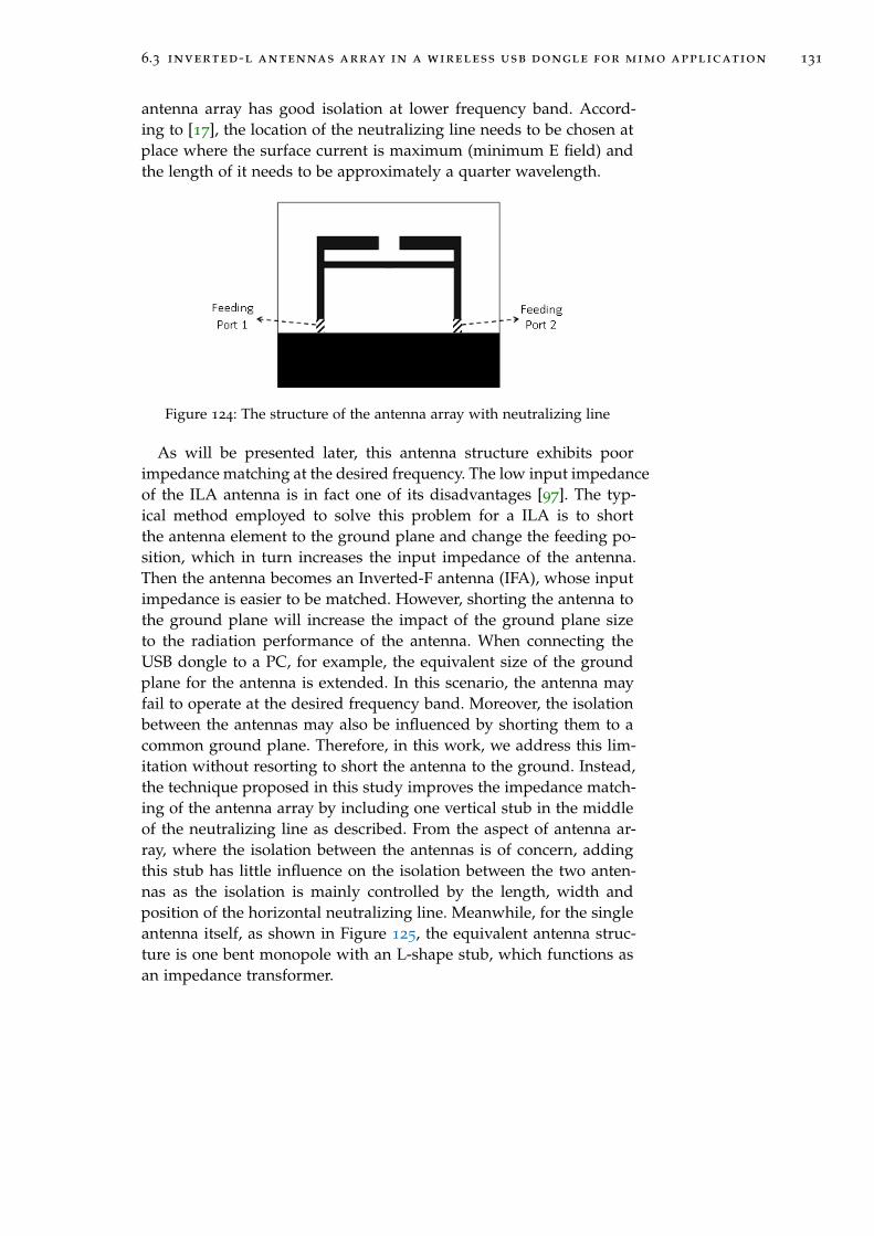
6.3 inverted-l antennas array in a wireless usb dongle for mimo application 131
antenna array has good isolation at lower frequency band. Accord-ing to [17], the location of the neutralizing line needs to be chosen atplace where the surface current is maximum (minimum E field) andthe length of it needs to be approximately a quarter wavelength.
Figure 124: The structure of the antenna array with neutralizing line
As will be presented later, this antenna structure exhibits poorimpedance matching at the desired frequency. The low input impedanceof the ILA antenna is in fact one of its disadvantages [97]. The typ-ical method employed to solve this problem for a ILA is to shortthe antenna element to the ground plane and change the feeding po-sition, which in turn increases the input impedance of the antenna.Then the antenna becomes an Inverted-F antenna (IFA), whose inputimpedance is easier to be matched. However, shorting the antenna tothe ground plane will increase the impact of the ground plane sizeto the radiation performance of the antenna. When connecting theUSB dongle to a PC, for example, the equivalent size of the groundplane for the antenna is extended. In this scenario, the antenna mayfail to operate at the desired frequency band. Moreover, the isolationbetween the antennas may also be influenced by shorting them to acommon ground plane. Therefore, in this work, we address this lim-itation without resorting to short the antenna to the ground. Instead,the technique proposed in this study improves the impedance match-ing of the antenna array by including one vertical stub in the middleof the neutralizing line as described. From the aspect of antenna ar-ray, where the isolation between the antennas is of concern, addingthis stub has little influence on the isolation between the two anten-nas as the isolation is mainly controlled by the length, width andposition of the horizontal neutralizing line. Meanwhile, for the singleantenna itself, as shown in Figure 125, the equivalent antenna struc-ture is one bent monopole with an L-shape stub, which functions asan impedance transformer.
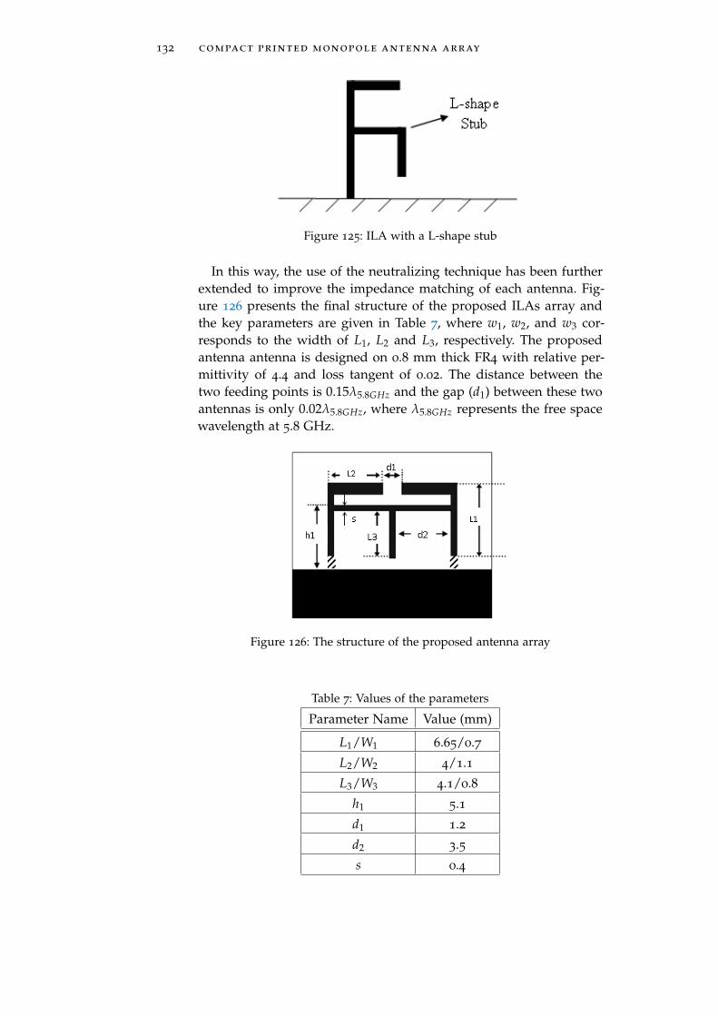
132 compact printed monopole antenna array
Figure 125: ILA with a L-shape stub
In this way, the use of the neutralizing technique has been furtherextended to improve the impedance matching of each antenna. Fig-ure 126 presents the final structure of the proposed ILAs array andthe key parameters are given in Table 7, where w1, w2, and w3 cor-responds to the width of L1, L2 and L3, respectively. The proposedantenna antenna is designed on 0.8 mm thick FR4 with relative per-mittivity of 4.4 and loss tangent of 0.02. The distance between thetwo feeding points is 0.15λ5.8GHz and the gap (d1) between these twoantennas is only 0.02λ5.8GHz, where λ5.8GHz represents the free spacewavelength at 5.8 GHz.
Figure 126: The structure of the proposed antenna array
Table 7: Values of the parameters
Parameter Name Value (mm)
L1/W1 6.65/0.7
L2/W2 4/1.1
L3/W3 4.1/0.8
h1 5.1
d1 1.2
d2 3.5
s 0.4

6.3 inverted-l antennas array in a wireless usb dongle for mimo application 133
6.3.3 Simulated and Measured Results
The fabricated prototype of the proposed antenna array is shown inFigure 127. Two semi-flexible cables were used to feed port 1 and port2 of the antenna array.
(a) Top view
(b) Back view
Figure 127: Photo of the fabricated ILA array
Figure 128 shows the measured return loss and isolation of theproposed antenna array. The measurement results suggest that theproposed ILA array has a 10 dB return loss bandwidth from 5.7 tomore than 6 GHz, which is more than the specification required forthe WLAN 5.8 GHz frequency band of interest (5.725 to 5.875 GHz).This makes the proposed antenna more robust during product inte-gration, such as proximity to other components and within the prod-uct enclosure, thus providing some margin against proximity effectswhich can lead to some frequency shifts. It is also found that the iso-lation between the two antennas is always better than 10 dB from 5.5to 6.0 GHz and within the desired WLAN operation band, an isola-tion of 12 dB or more is obtained. It is observed that there is somefrequency differences (less than 100 MHz) between the measured re-turn losses of the two ports of the antenna array. This is due to thefabrication accuracy and soldering of the feeding cable, which resultsin the asymmetrical response of the two antenna elements.
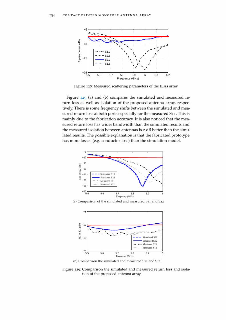
134 compact printed monopole antenna array
5.5 5.6 5.7 5.8 5.9 6 6.1 6.2−35
−25
−15
−5−5
Frequency (GHz)S
par
amet
ers
(dB
)
S11S22S21S12
Figure 128: Measured scattering parameters of the ILAs array
Figure 129 (a) and (b) compares the simulated and measured re-turn loss as well as isolation of the proposed antenna array, respec-tively. There is some frequency shifts between the simulated and mea-sured return loss at both ports especially for the measured S11. This ismainly due to the fabrication accuracy. It is also noticed that the mea-sured return loss has wider bandwidth than the simulated results andthe measured isolation between antennas is 2 dB better than the simu-lated results. The possible explanation is that the fabricated prototypehas more losses (e.g. conductor loss) than the simulation model.
5.5 5.6 5.7 5.8 5.9 6−40
−35
−30
−25
−20
−15
−10
−5
Frequency (GHz)
S11
or S
22 (
dB)
Simulated S11
Simulated S22
Measured S11
Measured S22
(a) Comparison of the simulated and measured S11 and S22
5.5 5.6 5.7 5.8 5.9 66−20
−15
−10
−5−5
Frequency (GHz)
S12
or S
21 (
dB)
Simulated S21
Simulated S12
Measured S21
Measured S12
(b) Comparison the simulated and measured S21 and S12
Figure 129: Comparison the simulated and measured return loss and isola-tion of the proposed antenna array
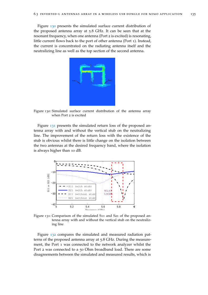
6.3 inverted-l antennas array in a wireless usb dongle for mimo application 135
Figure 130 presents the simulated surface current distribution ofthe proposed antenna array at 5.8 GHz. It can be seen that at theresonant frequency, when one antenna (Port 2 is excited) is resonating,little current flows back to the port of other antenna (Port 1). Instead,the current is concentrated on the radiating antenna itself and theneutralizing line as well as the top section of the second antenna.
Figure 130: Simulated surface current distribution of the antenna arraywhen Port 2 is excited
Figure 131 presents the simulated return loss of the proposed an-tenna array with and without the vertical stub on the neutralizingline. The improvement of the return loss with the existence of thestub is obvious whilst there is little change on the isolation betweenthe two antennas at the desired frequency band, where the isolationis always higher than 10 dB.
5 5.2 5.4 5.6 5.8 66−40
−30
−20
−10
00
Frequency (GHz)
S11orS21(dB)
S11 (with stub)
S21 (with stub)
S11 (without stub)
S21 (without stub)
WLAN5.8GHz
Figure 131: Comparison of the simulated S11 and S21 of the proposed an-tenna array with and without the vertical stub on the neutraliz-ing line
Figure 132 compares the simulated and measured radiation pat-terns of the proposed antenna array at 5.8 GHz. During the measure-ment, the Port 1 was connected to the network analyzer whilst thePort 2 was connected to a 50 Ohm broadband load. There are somedisagreements between the simulated and measured results, which is
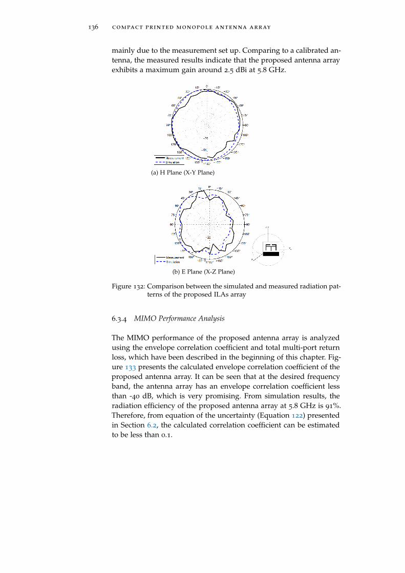
136 compact printed monopole antenna array
mainly due to the measurement set up. Comparing to a calibrated an-tenna, the measured results indicate that the proposed antenna arrayexhibits a maximum gain around 2.5 dBi at 5.8 GHz.
(a) H Plane (X-Y Plane)
(b) E Plane (X-Z Plane)
Figure 132: Comparison between the simulated and measured radiation pat-terns of the proposed ILAs array
6.3.4 MIMO Performance Analysis
The MIMO performance of the proposed antenna array is analyzedusing the envelope correlation coefficient and total multi-port returnloss, which have been described in the beginning of this chapter. Fig-ure 133 presents the calculated envelope correlation coefficient of theproposed antenna array. It can be seen that at the desired frequencyband, the antenna array has an envelope correlation coefficient lessthan -40 dB, which is very promising. From simulation results, theradiation efficiency of the proposed antenna array at 5.8 GHz is 91%.Therefore, from equation of the uncertainty (Equation 122) presentedin Section 6.2, the calculated correlation coefficient can be estimatedto be less than 0.1.
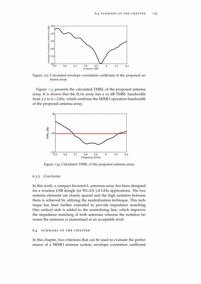
6.4 summary of the chapter 137
5.5 5.6 5.7 5.8 5.9 6 6.1 6.2−80
−70
−60
−50
−40
−30
Frequency (dB)
Env
elop
e C
orre
latio
n C
oeff
icen
cy (
dB)
Figure 133: Calculated envelope correlation coefficient of the proposed an-tenna array
Figure 134 presents the calculated TMRL of the proposed antennaarray. It is shown that the ILAs array has a 10 dB TMRL bandwidthfrom 5.7 to 6.1 GHz, which confirms the MIMO operation bandwidthof the proposed antenna array.
5.5 5.6 5.7 5.8 5.9 6 6.1 6.2−15
−10
−5−5
Frequency (GHz)
TM
RL
(dB
)
Figure 134: Calculated TMRL of the proposed antenna array
6.3.5 Conclusion
In this work, a compact Inverted-L antennas array has been designedfor a wireless USB dongle for WLAN 5.8 GHz applications. The twoantenna elements are closely spaced and the high isolation betweenthem is achieved by utilizing the neutralization technique. This tech-nique has been further extended to provide impedance matching.One vertical stub is added to the neutralizing line, which improvesthe impedance matching of both antennas whereas the isolation be-tween the antennas is maintained at an acceptable level.
6.4 summary of the chapter
In this chapter, two criterions that can be used to evaluate the perfor-mance of a MIMO antenna system, envelope correlation coefficient

138 compact printed monopole antenna array
and total multi-port return loss, are introduced. Then, one compactsize inverted-L antenna array is proposed for the WLAN 5.8 GHzapplication. The antennas are closely spaced and the main methodol-ogy used to increase the isolation of the two antennas is to employthe ‘neutralizing technique’. This technique was firstly proposed todesign the single band PIFA array and in this work, it has been inno-vatively used in the design of printed ILA antenna array. Moreover,in the proposed antenna array, the neutralizing line was also used forthe purpose of impedance matching. The measurement results showthat the proposed antenna array has a wide operational frequencybandwidth and isolation better than 10 dB over the frequency bandof interest.
The work presented in this chapter will be published in:
1. Q. Luo; C. Quigley; J. Pereira and H. M Salgado. Inverted-L An-tennas Array in a Wireless USB Dongle for MIMO Application.In Proceedings of 6th European Conference on Antennas and Propa-gation (EuCAP), Prague, Czech Republic, March 2012.

Part III
R E C O N F I G U R A B L E A N T E N N A D E S I G N

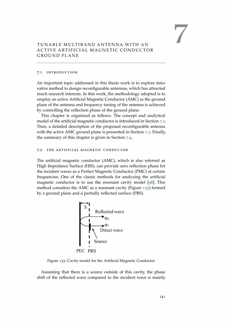
7T U N A B L E M U LT I B A N D A N T E N N A W I T H A NA C T I V E A RT I F I C I A L M A G N E T I C C O N D U C T O RG R O U N D P L A N E
7.1 introduction
An important topic addressed in this thesis work is to explore inno-vative method to design reconfigurable antennas, which has attractedmuch research interests. In this work, the methodology adopted is toemploy an active Artificial Magnetic Conductor (AMC) as the groundplane of the antenna and frequency tuning of the antenna is achievedby controlling the reflection phase of the ground plane.
This chapter is organized as follows. The concept and analyticalmodel of the artificial magnetic conductor is introduced in Section 7.2.Then, a detailed description of the proposed reconfigurable antennawith the active AMC ground plane is presented in Section 7.3. Finally,the summary of this chapter is given in Section 7.4.
7.2 the artificial magnetic conductor
The artificial magnetic conductor (AMC), which is also referred asHigh Impedance Surface (HIS), can provide zero reflection phase forthe incident waves as a Perfect Magnetic Conductor (PMC) at certainfrequencies. One of the classic methods for analyzing the artificialmagnetic conductor is to use the resonant cavity model [98]. Thismethod considers the AMC as a resonant cavity (Figure 135) formedby a ground plane and a partially reflected surface (PRS).
Figure 135: Cavity model for the Artificial Magnetic Conductor
Assuming that there is a source outside of this cavity, the phaseshift of the reflected wave compared to the incident wave is mainly
141
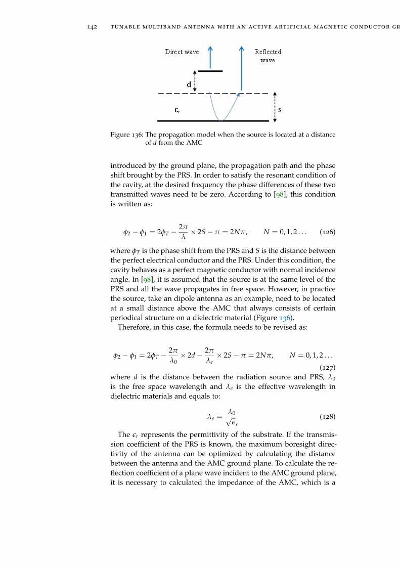
142 tunable multiband antenna with an active artificial magnetic conductor ground plane
Figure 136: The propagation model when the source is located at a distanceof d from the AMC
introduced by the ground plane, the propagation path and the phaseshift brought by the PRS. In order to satisfy the resonant condition ofthe cavity, at the desired frequency the phase differences of these twotransmitted waves need to be zero. According to [98], this conditionis written as:
φ2 − φ1 = 2φT −2π
λ× 2S− π = 2Nπ, N = 0, 1, 2 . . . (126)
where φT is the phase shift from the PRS and S is the distance betweenthe perfect electrical conductor and the PRS. Under this condition, thecavity behaves as a perfect magnetic conductor with normal incidenceangle. In [98], it is assumed that the source is at the same level of thePRS and all the wave propagates in free space. However, in practicethe source, take an dipole antenna as an example, need to be locatedat a small distance above the AMC that always consists of certainperiodical structure on a dielectric material (Figure 136).
Therefore, in this case, the formula needs to be revised as:
φ2 − φ1 = 2φT −2π
λ0× 2d− 2π
λe× 2S− π = 2Nπ, N = 0, 1, 2 . . .
(127)where d is the distance between the radiation source and PRS, λ0
is the free space wavelength and λe is the effective wavelength indielectric materials and equals to:
λe =λ0√
εr(128)
The εr represents the permittivity of the substrate. If the transmis-sion coefficient of the PRS is known, the maximum boresight direc-tivity of the antenna can be optimized by calculating the distancebetween the antenna and the AMC ground plane. To calculate the re-flection coefficient of a plane wave incident to the AMC ground plane,it is necessary to calculated the impedance of the AMC, which is a
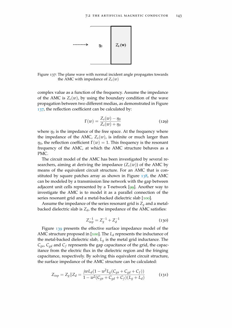
7.2 the artificial magnetic conductor 143
Figure 137: The plane wave with normal incident angle propagates towardsthe AMC with impedance of Zs(w)
complex value as a function of the frequency. Assume the impedanceof the AMC is Zs(w), by using the boundary condition of the wavepropagation between two different medias, as demonstrated in Figure137, the reflection coefficient can be calculated by:
Γ(w) =Zs(w)− η0
Zs(w) + η0(129)
where η0 is the impedance of the free space. At the frequency wherethe impedance of the AMC, Zs(w), is infinite or much larger thanη0, the reflection coefficient Γ(w) = 1. This frequency is the resonantfrequency of the AMC, at which the AMC structure behaves as aPMC.
The circuit model of the AMC has been investigated by several re-searchers, aiming at deriving the impedance (Zs(w)) of the AMC bymeans of the equivalent circuit structure. For an AMC that is con-stituted by square patches array as shown in Figure 138, the AMCcan be modeled by a transmission line network with the gap betweenadjacent unit cells represented by a T-network [99]. Another way toinvestigate the AMC is to model it as a parallel connection of theseries resonant grid and a metal-backed dielectric slab [100].
Assume the impedance of the series resonant grid is Zg and a metal-backed dielectric slab is Zd, the the impedance of the AMC satisfies:
Z−1inp = Z−1
g + Z−1d (130)
Figure 139 presents the effective surface impedance model of theAMC structure proposed in [100]. The Ld represents the inductance ofthe metal-backed dielectric slab, Lg is the metal grid inductance. TheCga, Cgd and C f represents the gap capacitance of the grid, the capac-itance from the electric flux in the dielectric region and the fringingcapacitance, respectively. By solving this equivalent circuit structure,the surface impedance of the AMC structure can be calculated:
Zinp = Zg‖Zd =jwLd(1− w2Lg(Cga + Cgd + C f ))
1− w2(Cga + Cgd + C f )(Lg + Ld)(131)
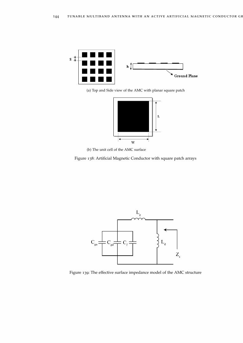
144 tunable multiband antenna with an active artificial magnetic conductor ground plane
(a) Top and Side view of the AMC with planar square patch
(b) The unit cell of the AMC surface
Figure 138: Artificial Magnetic Conductor with square patch arrays
Figure 139: The effective surface impedance model of the AMC structure
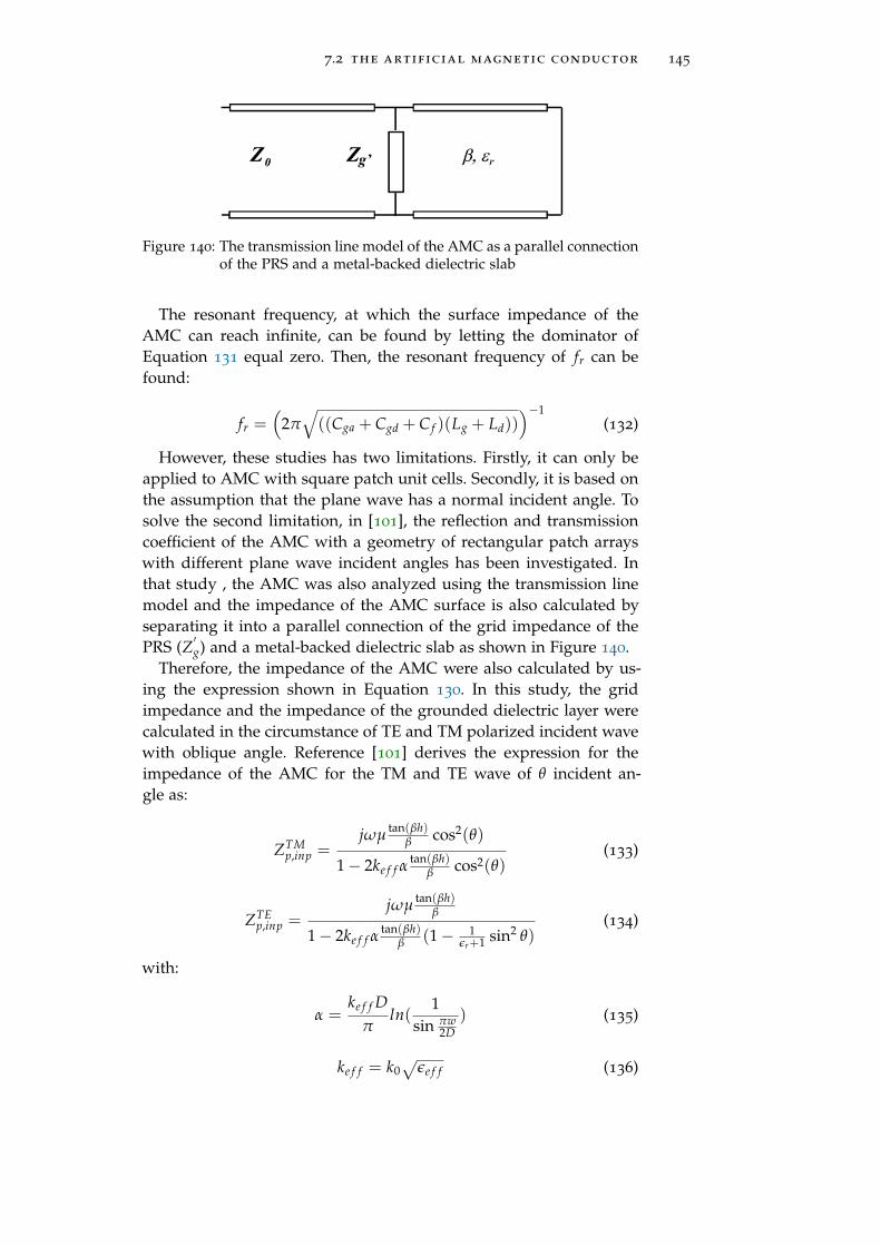
7.2 the artificial magnetic conductor 145
Figure 140: The transmission line model of the AMC as a parallel connectionof the PRS and a metal-backed dielectric slab
The resonant frequency, at which the surface impedance of theAMC can reach infinite, can be found by letting the dominator ofEquation 131 equal zero. Then, the resonant frequency of fr can befound:
fr =(
2π√((Cga + Cgd + C f )(Lg + Ld))
)−1(132)
However, these studies has two limitations. Firstly, it can only beapplied to AMC with square patch unit cells. Secondly, it is based onthe assumption that the plane wave has a normal incident angle. Tosolve the second limitation, in [101], the reflection and transmissioncoefficient of the AMC with a geometry of rectangular patch arrayswith different plane wave incident angles has been investigated. Inthat study , the AMC was also analyzed using the transmission linemodel and the impedance of the AMC surface is also calculated byseparating it into a parallel connection of the grid impedance of thePRS (Z
′g) and a metal-backed dielectric slab as shown in Figure 140.
Therefore, the impedance of the AMC were also calculated by us-ing the expression shown in Equation 130. In this study, the gridimpedance and the impedance of the grounded dielectric layer werecalculated in the circumstance of TE and TM polarized incident wavewith oblique angle. Reference [101] derives the expression for theimpedance of the AMC for the TM and TE wave of θ incident an-gle as:
ZTMp,inp =
jωµtan(βh)
β cos2(θ)
1− 2ke f f αtan(βh)
β cos2(θ)(133)
ZTEp,inp =
jωµtan(βh)
β
1− 2ke f f αtan(βh)
β (1− 1εr+1 sin2 θ)
(134)
with:
α =ke f f D
πln(
1sin πw
2D) (135)
ke f f = k0√
εe f f (136)
146 tunable multiband antenna with an active artificial magnetic conductor ground plane
β =√
k2 − k2t (137)
where k is the wave number in the substrate material and kt is thetangential wave number component imposed by the incident wave. Itis known that the impedance of the TE and TM waves are:
ZTE0 =
η0
cos θ(138)
ZTM0 = η0 cos θ (139)
Therefore, the reflection coefficient of the TE and TM wave withdifferent incident angle can be calculated from:
ΓTE(w) =ZTE
s (w)− ZTE0
ZTEs (w) + ZTE
0(140)
ΓTM(w) =ZTM
s (w)− ZTM0
ZTMs (w) + ZTM
0(141)
The formulas developed by [101] can provide a good predictionof the reflection coefficient of the AMC with an arbitrary polarizationand incident angle. However, this method is again limited to the AMCwith square patch structures as was the case of the theoretical modelproposed by [99]. For certain specific geometries, such as JerusalemCross based AMC, the estimation of its characteristics was investi-gated in [102]. However, regarding the AMC with more complex sur-face patterns, with which the AMC can be designed for operating atlower frequencies or multiple frequencies with a reduced size, cur-rently there is no general model that can be applied. Therefore, themost common technique to design compact size AMC structure isto based on the analysis of general characteristics of AMCs and per-forming EM simulations using FDTD or FEM methods to get moreaccurate results.
7.3 reconfigurable antenna with active amc
7.3.1 Motivation
Reconfiguration of antenna provides the possibility of designing an-tennas of more compact size whilst operating in several frequencybands. One of the most common methods to make an antenna recon-figurable is to change the electrical length or impedance matching ofthe antenna by directly adding some RF switches such as PIN diodeor MEMS (Micro-electromechanical Systems) switches on the radia-tion element. In [103], a coplanar antenna that can operate from 4.9to 5.4 GHz was achieved by adding a varactor between the squarepatch and the surrounding ground plane. Upon using a large num-
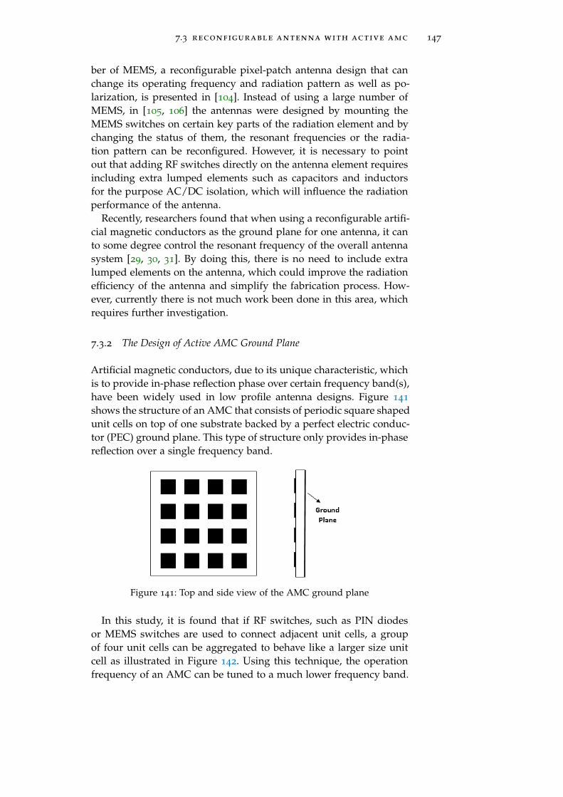
7.3 reconfigurable antenna with active amc 147
ber of MEMS, a reconfigurable pixel-patch antenna design that canchange its operating frequency and radiation pattern as well as po-larization, is presented in [104]. Instead of using a large number ofMEMS, in [105, 106] the antennas were designed by mounting theMEMS switches on certain key parts of the radiation element and bychanging the status of them, the resonant frequencies or the radia-tion pattern can be reconfigured. However, it is necessary to pointout that adding RF switches directly on the antenna element requiresincluding extra lumped elements such as capacitors and inductorsfor the purpose AC/DC isolation, which will influence the radiationperformance of the antenna.
Recently, researchers found that when using a reconfigurable artifi-cial magnetic conductors as the ground plane for one antenna, it canto some degree control the resonant frequency of the overall antennasystem [29, 30, 31]. By doing this, there is no need to include extralumped elements on the antenna, which could improve the radiationefficiency of the antenna and simplify the fabrication process. How-ever, currently there is not much work been done in this area, whichrequires further investigation.
7.3.2 The Design of Active AMC Ground Plane
Artificial magnetic conductors, due to its unique characteristic, whichis to provide in-phase reflection phase over certain frequency band(s),have been widely used in low profile antenna designs. Figure 141
shows the structure of an AMC that consists of periodic square shapedunit cells on top of one substrate backed by a perfect electric conduc-tor (PEC) ground plane. This type of structure only provides in-phasereflection over a single frequency band.
Figure 141: Top and side view of the AMC ground plane
In this study, it is found that if RF switches, such as PIN diodesor MEMS switches are used to connect adjacent unit cells, a groupof four unit cells can be aggregated to behave like a larger size unitcell as illustrated in Figure 142. Using this technique, the operationfrequency of an AMC can be tuned to a much lower frequency band.
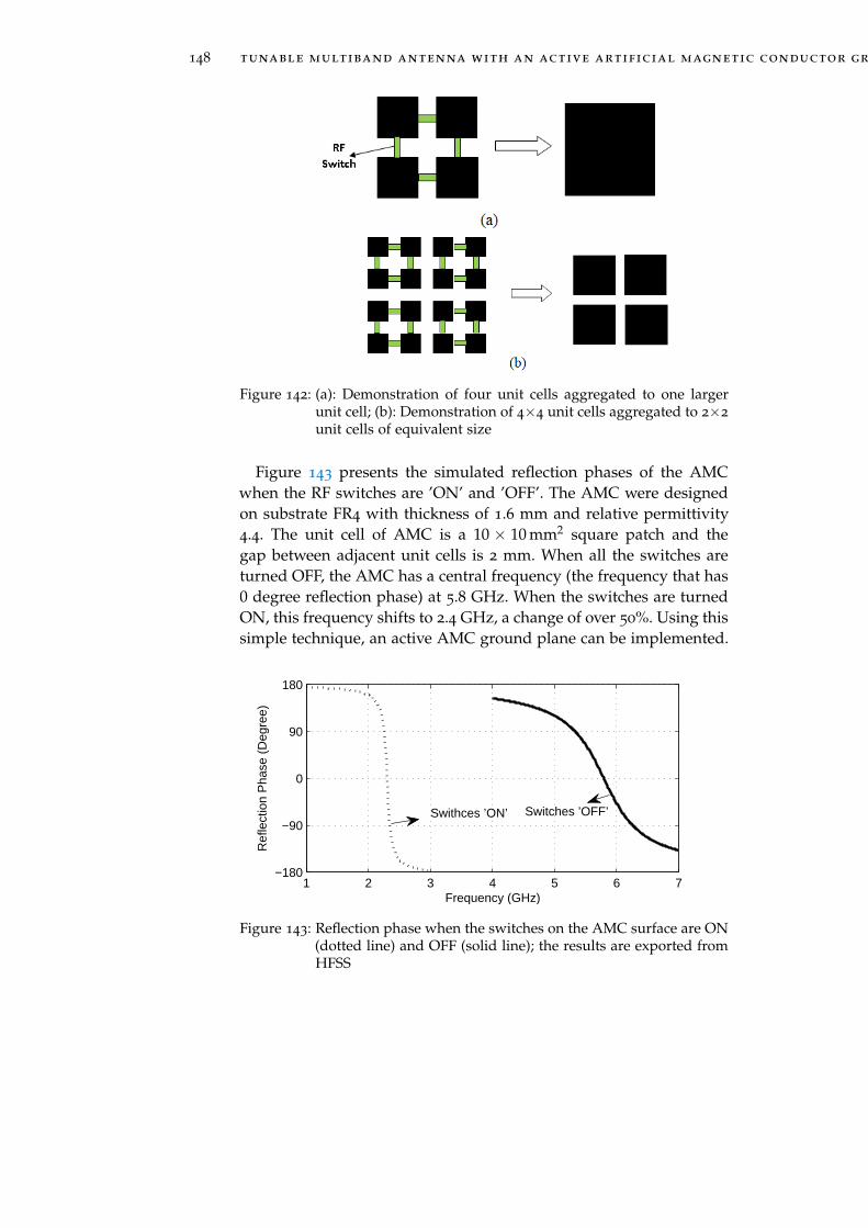
148 tunable multiband antenna with an active artificial magnetic conductor ground plane
Figure 142: (a): Demonstration of four unit cells aggregated to one largerunit cell; (b): Demonstration of 4×4 unit cells aggregated to 2×2
unit cells of equivalent size
Figure 143 presents the simulated reflection phases of the AMCwhen the RF switches are ’ON’ and ’OFF’. The AMC were designedon substrate FR4 with thickness of 1.6 mm and relative permittivity4.4. The unit cell of AMC is a 10 × 10 mm2 square patch and thegap between adjacent unit cells is 2 mm. When all the switches areturned OFF, the AMC has a central frequency (the frequency that has0 degree reflection phase) at 5.8 GHz. When the switches are turnedON, this frequency shifts to 2.4 GHz, a change of over 50%. Using thissimple technique, an active AMC ground plane can be implemented.
1 2 3 4 5 6 7−180
−90
0
90
180
Frequency (GHz)
Ref
lect
ion
Pha
se (
Deg
ree)
Switches ’OFF’Swithces ’ON’
Figure 143: Reflection phase when the switches on the AMC surface are ON(dotted line) and OFF (solid line); the results are exported fromHFSS
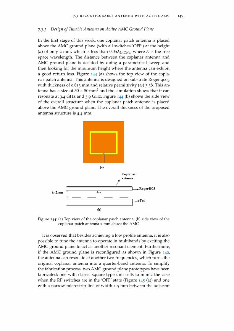
7.3 reconfigurable antenna with active amc 149
7.3.3 Design of Tunable Antenna on Active AMC Ground Plane
In the first stage of this work, one coplanar patch antenna is placedabove the AMC ground plane (with all switches ‘OFF’) at the height(h) of only 2 mm, which is less than 0.05λ2.4GHz, where λ is the freespace wavelength. The distance between the coplanar antenna andAMC ground plane is decided by doing a parametrical sweep andthen looking for the minimum height where the antenna can exhibita good return loss. Figure 144 (a) shows the top view of the copla-nar patch antenna. This antenna is designed on substrate Roger 4003
with thickness of 0.813 mm and relative permittivity (εr) 3.38. This an-tenna has a size of 50× 50 mm2 and the simulation shows that it canresonate at 3.4 GHz and 5.9 GHz. Figure 144 (b) shows the side viewof the overall structure when the coplanar patch antenna is placedabove the AMC ground plane. The overall thickness of the proposedantenna structure is 4.4 mm.
Figure 144: (a) Top view of the coplanar patch antenna; (b) side view of thecoplanar patch antenna 2 mm above the AMC
It is observed that besides achieving a low profile antenna, it is alsopossible to tune the antenna to operate in multibands by exciting theAMC ground plane to act as another resonant element. Furthermore,if the AMC ground plane is reconfigured as shown in Figure 142,the antenna can resonate at another two frequencies, which turns theoriginal coplanar antenna into a quarter-band antenna. To simplifythe fabrication process, two AMC ground plane prototypes have beenfabricated: one with classic square type unit cells to mimic the casewhen the RF switches are in the ’OFF’ state (Figure 145 (a)) and onewith a narrow microstrip line of width 1.5 mm between the adjacent
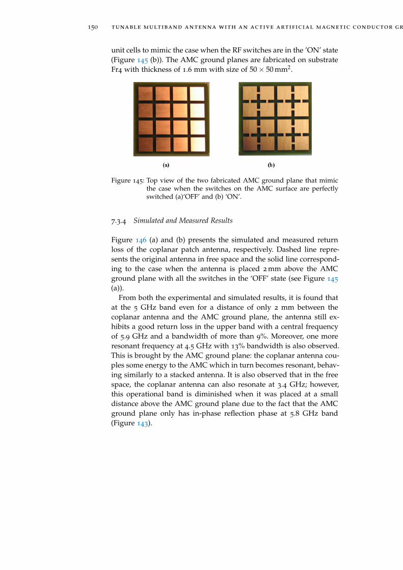
150 tunable multiband antenna with an active artificial magnetic conductor ground plane
unit cells to mimic the case when the RF switches are in the ’ON’ state(Figure 145 (b)). The AMC ground planes are fabricated on substrateFr4 with thickness of 1.6 mm with size of 50× 50 mm2.
Figure 145: Top view of the two fabricated AMC ground plane that mimicthe case when the switches on the AMC surface are perfectlyswitched (a)‘OFF’ and (b) ‘ON’.
7.3.4 Simulated and Measured Results
Figure 146 (a) and (b) presents the simulated and measured returnloss of the coplanar patch antenna, respectively. Dashed line repre-sents the original antenna in free space and the solid line correspond-ing to the case when the antenna is placed 2 mm above the AMCground plane with all the switches in the ‘OFF’ state (see Figure 145
(a)).From both the experimental and simulated results, it is found that
at the 5 GHz band even for a distance of only 2 mm between thecoplanar antenna and the AMC ground plane, the antenna still ex-hibits a good return loss in the upper band with a central frequencyof 5.9 GHz and a bandwidth of more than 9%. Moreover, one moreresonant frequency at 4.5 GHz with 13% bandwidth is also observed.This is brought by the AMC ground plane: the coplanar antenna cou-ples some energy to the AMC which in turn becomes resonant, behav-ing similarly to a stacked antenna. It is also observed that in the freespace, the coplanar antenna can also resonate at 3.4 GHz; however,this operational band is diminished when it was placed at a smalldistance above the AMC ground plane due to the fact that the AMCground plane only has in-phase reflection phase at 5.8 GHz band(Figure 143).
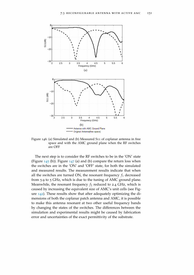
7.3 reconfigurable antenna with active amc 151
2 2.5 3 3.5 4 4.5 5 5.5 6−30
−20
−10
00
Frequency (GHz)
S11
(dB
)
(a)
2 2.5 3 3.5 4 4.5 5 5.5 6−30
−20
−10
00
Frequnecy (GHz)
S11
(dB
)
(b)
Figure 146: (a) Simulated and (b) Measured S11 of coplanar antenna in freespace and with the AMC ground plane when the RF switchesare OFF
The next step is to consider the RF switches to be in the ’ON’ state(Figure 145 (b)). Figure 147 (a) and (b) compare the return loss whenthe switches are in the ’ON’ and ’OFF’ state, for both the simulatedand measured results. The measurement results indicate that whenall the switches are turned ON, the resonant frequency f1 decreasedfrom 5.9 to 5 GHz, which is due to the tuning of AMC ground plane.Meanwhile, the resonant frequency f2 reduced to 2.4 GHz, which iscaused by increasing the equivalent size of AMC’s unit cells (see Fig-ure 142). These results show that after adequately optimizing the di-mensions of both the coplanar patch antenna and AMC, it is possibleto make this antenna resonant at two other useful frequency bandsby changing the states of the switches. The differences between thesimulation and experimental results might be caused by fabricationerror and uncertainties of the exact permittivity of the substrate.
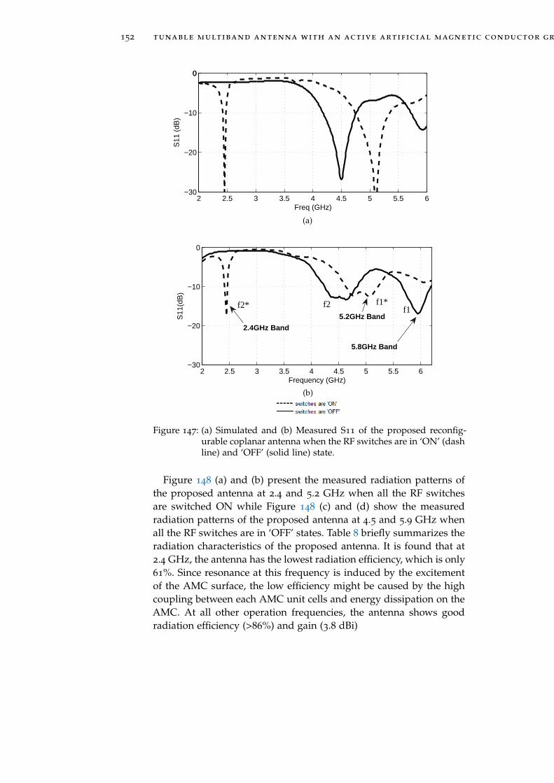
152 tunable multiband antenna with an active artificial magnetic conductor ground plane
2 2.5 3 3.5 4 4.5 5 5.5 6−30
−20
−10
00
Freq (GHz)
S11
(dB
)
(a)
2 2.5 3 3.5 4 4.5 5 5.5 6−30
−20
−10
0
Frequency (GHz)
S11
(dB
)
2.4GHz Band
5.2GHz Band
5.8GHz Band
f2* f2 f1*f1
(b)
Figure 147: (a) Simulated and (b) Measured S11 of the proposed reconfig-urable coplanar antenna when the RF switches are in ‘ON’ (dashline) and ‘OFF’ (solid line) state.
Figure 148 (a) and (b) present the measured radiation patterns ofthe proposed antenna at 2.4 and 5.2 GHz when all the RF switchesare switched ON while Figure 148 (c) and (d) show the measuredradiation patterns of the proposed antenna at 4.5 and 5.9 GHz whenall the RF switches are in ‘OFF’ states. Table 8 briefly summarizes theradiation characteristics of the proposed antenna. It is found that at2.4 GHz, the antenna has the lowest radiation efficiency, which is only61%. Since resonance at this frequency is induced by the excitementof the AMC surface, the low efficiency might be caused by the highcoupling between each AMC unit cells and energy dissipation on theAMC. At all other operation frequencies, the antenna shows goodradiation efficiency (>86%) and gain (3.8 dBi)
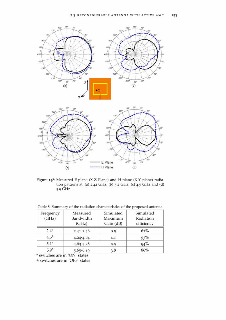
7.3 reconfigurable antenna with active amc 153
Figure 148: Measured E-plane (X-Z Plane) and H-plane (X-Y plane) radia-tion patterns at: (a) 2.42 GHz, (b) 5.2 GHz, (c) 4.5 GHz and (d)5.9 GHz
Table 8: Summary of the radiation characteristics of the proposed antenna
Frequency(GHz)
MeasuredBandwidth
(GHz)
SimulatedMaximumGain (dB)
SimulatedRadiationefficiency
2.4∗ 2.41-2.46 0.5 61%
4.5#4.24-4.84 4.1 93%
5.1∗ 4.63-5.26 5.5 94%
5.9#5.65-6.19 3.8 86%
* switches are in ‘ON’ states# switches are in ‘OFF’ states
154 tunable multiband antenna with an active artificial magnetic conductor ground plane
7.3.5 Conclusion
In this work, a new tunable coplanar patch antenna with an activeAMC ground plane has been presented. It is shown that by using theAMC as the ground plane, not only one can design a low profile copla-nar antenna, but also can turn the antenna to have an added func-tionality which is a tunable multiband operation characteristic. Withthe active AMC ground plane that can be reconfigured by switch-ing ON/OFF the RF switches, experimental results show that thisproposed AMC coplanar antenna can operate at four different bands:2.41-2.46 GHz, 4.24-4.84 GHz, 4.63-5.26 GHz and 5.65-6.19 GHz. Theseinclude almost the entire required bands for WLAN 802.11a/b/g ap-plications. Future work, besides further optimizing the overall an-tenna performance, involves mounting the RF switches on the sur-face of AMC and evaluating the influence of the RF switches on theperformance of the AMC comparing it to the ideal case.
7.4 summary of the chapter
The reconfigurable antenna presented in this chapter is based on theconcept of active AMC ground plane. Artificial magnetic conductors,due to its unique characteristic, which is to provide in-phase reflec-tion phase over certain frequency band(s), have been widely used inlow profile antenna designs. Some analytical methods that can beused to analyzing the AMC structure are presented in the beginningof this chapter. For AMC with complex geometries, using numeri-cal methods is required. Our investigations indicate that an antenna(in this study, one coplanar antenna is chosen) with different AMCground plane can exhibit different resonant frequencies. Therefore,based on these findings, it is decided to mount RF switches on thesurface of the AMC that consists of periodic square elements to makeit be reconfigurable. By optimizing the dimensions of the AMC andthe distance between the AMC and coplanar antenna, the resonantfrequency of the coplanar antenna can be reconfigured by using suchan active AMC ground plane, whose reflection phase is controlledby the states of the RF switches. Moreover, it is also observed thatadditional resonant frequency can be created by using the coplanarantenna as a main radiator and the AMC as a coupled element, whichbehave similar to an antenna of stacked structure.
It is important to point out that in both studies the RF switchesare substituted by a short microstrip line to mimic that case that theswitches are ‘ON’ and a small gap to mimic the case that the switchesare perfectly ‘OFF’. This simplifies the fabrication process; however,it ignores the additional losses introduced by the RF switches, whichneed to be further investigated in future works. This work has beenpublished in:

7.4 summary of the chapter 155
1. Q. Luo; J.R. Pereira and H.M. Salgado. Tunable Multiband An-tenna With An Active Artificial Magnetic Conductor GroundPlane. In Proceedings of European Microwave Conference (EuMC),Paris, France, October 2010.

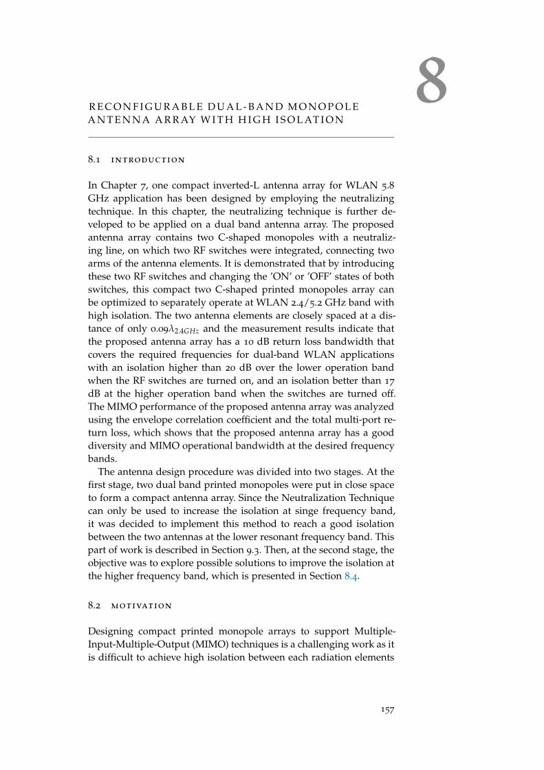
8R E C O N F I G U R A B L E D U A L - B A N D M O N O P O L EA N T E N N A A R R AY W I T H H I G H I S O L AT I O N
8.1 introduction
In Chapter 7, one compact inverted-L antenna array for WLAN 5.8GHz application has been designed by employing the neutralizingtechnique. In this chapter, the neutralizing technique is further de-veloped to be applied on a dual band antenna array. The proposedantenna array contains two C-shaped monopoles with a neutraliz-ing line, on which two RF switches were integrated, connecting twoarms of the antenna elements. It is demonstrated that by introducingthese two RF switches and changing the ’ON’ or ’OFF’ states of bothswitches, this compact two C-shaped printed monopoles array canbe optimized to separately operate at WLAN 2.4/5.2 GHz band withhigh isolation. The two antenna elements are closely spaced at a dis-tance of only 0.09λ2.4GHz and the measurement results indicate thatthe proposed antenna array has a 10 dB return loss bandwidth thatcovers the required frequencies for dual-band WLAN applicationswith an isolation higher than 20 dB over the lower operation bandwhen the RF switches are turned on, and an isolation better than 17
dB at the higher operation band when the switches are turned off.The MIMO performance of the proposed antenna array was analyzedusing the envelope correlation coefficient and the total multi-port re-turn loss, which shows that the proposed antenna array has a gooddiversity and MIMO operational bandwidth at the desired frequencybands.
The antenna design procedure was divided into two stages. At thefirst stage, two dual band printed monopoles were put in close spaceto form a compact antenna array. Since the Neutralization Techniquecan only be used to increase the isolation at singe frequency band,it was decided to implement this method to reach a good isolationbetween the two antennas at the lower resonant frequency band. Thispart of work is described in Section 9.3. Then, at the second stage, theobjective was to explore possible solutions to improve the isolation atthe higher frequency band, which is presented in Section 8.4.
8.2 motivation
Designing compact printed monopole arrays to support Multiple-Input-Multiple-Output (MIMO) techniques is a challenging work as itis difficult to achieve high isolation between each radiation elements
157
158 reconfigurable dual-band monopole antenna array with high isolation
when they are closely spaced. The existent proposed methods, suchas the use of metallic Electromagnetic Band Gap structures on thesubstrate of the antennas [15] or the Defect Ground System [16] onthe ground plane, although they can effectively improve the isolationbetween two closely space antennas, they are difficult to integrateinto the overall system. So far, there are few studies addressing com-pact multi-band MIMO antenna array designs. In [95], a dual bandtwo antenna array was proposed for USB dongle application. Thisantenna consists of an L-shape patch and a via trace connecting thevia to the ground. Besides the complicated fabrication process, theexperimental result provided in [95] shows that the isolation of theantenna array at 2.4 GHz is less than 9 dB. A printed coplanar two-antenna element for 2.4/5 GHz WLAN operation in a MIMO systemwas presented in [107]. This design employed two single band anten-nas, which were independently located at the two ends of the PCBboard, to realize the dual band operation and high isolation betweeneach other. However, this design is not a real MIMO antenna array asit only contains two single band antennas, each of which resonates atdifferent resonant frequency.
The Neutralization Techniques recently proposed in [17] has been suc-cessfully applied to the design of a compact ILA array for single bandWLAN application in Chapter 7. The neutralizing technique providesan alternative feasible solution to design compact MIMO antenna ar-rays within limited space. Using this method, the isolation of twoantennas could be improved through neutralizing the current of twoantennas without the need for adding extra space for antenna de-sign. However, this technique has only be applied to the design ofantenna arrays operating at single frequency band and there are notmuch studies investigating it. Therefore, in this work, it aims to fur-ther investigate this technique and apply it to the dual band printedmonopole antenna design.
8.3 single band compact antenna array for wlan 2 .4ghz
8.3.1 Antenna Structure
As described before, the design procedure involves two stages. Atthe first stage, two printed monopole antennas were put in closespace to form a compact antenna array. The geometry of the pro-posed printed C-shaped monopole antenna array with high isolationat 2.4 GHz band is shown in Figure 149. This antenna is designedon substrate Roger 4003 with thickness of 0.813 mm and relative per-mittivity of 3.38. The antenna element is printed on one side of thesubstrate while the ground plane is located at the other side. Figure149 (a), (b) and (c) present the top, back and side view of the pro-
8.3 single band compact antenna array for wlan 2 .4 ghz 159
posed monopole array, respectively. The width of the microstrip lineis 1.12 mm and the total length of the C-shape is 36.5 mm. The twoC-shaped monopoles are located symmetrically at the left and rightside of the substrate and the distance between the two feeding linesis only 11.8 mm, which is around 0.09λ2.4GHz, where λ2.4GHz repre-sents the free space wavelength at 2.4 GHz. There is a 0.5 mm wideshorting line connecting the two arms of the monopoles, which takesthe role of neutralizing the currents from two monopole antennas toincrease their isolation.
Figure 149: (a)Top view, (b)back view and (c) side view of the proposedantenna array
It is found that the resonant frequency at 2.4 GHz is mainly deter-mined by the total length of the C-shape radiation element. By suit-ably selecting the total length of the C-shape, the desired resonantfrequency can be achieved. Actually this printed monopole antennacan also resonate at another higher frequency; however, at this stage,it only aims to make this antenna array operate properly at the lowerband. The operation at the higher band was ignored at this stagebut will be investigated in the next stage. The isolation at the de-sired frequency band is determined by the length of the neutralizingline and its position. According to [17], the neutralizing line shouldbe placed at the position where is surface current is strong (to min-imize the influence of the neutralizing line to the original resonantfrequency) and the length of it should be approximately a quarterwavelength. Therefore, it can be concluded that after introducing theneutralizing line, in order to achieve the optimum performance interms of both return loss and isolation at the frequency band of in-
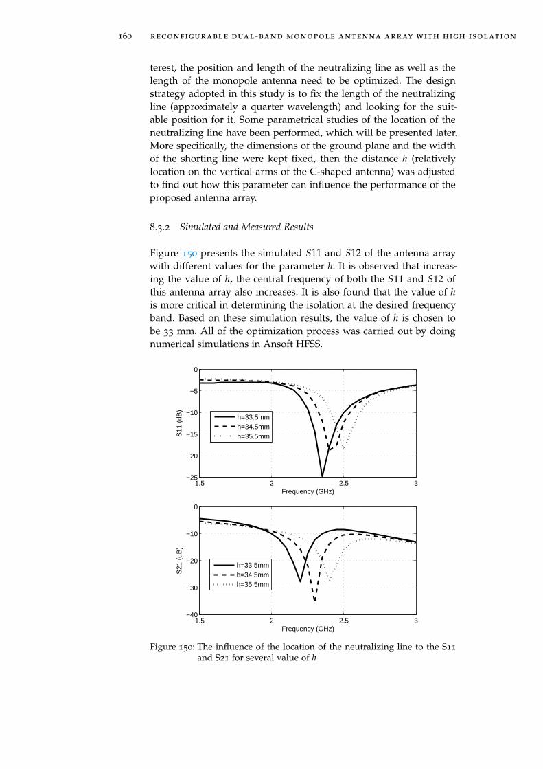
160 reconfigurable dual-band monopole antenna array with high isolation
terest, the position and length of the neutralizing line as well as thelength of the monopole antenna need to be optimized. The designstrategy adopted in this study is to fix the length of the neutralizingline (approximately a quarter wavelength) and looking for the suit-able position for it. Some parametrical studies of the location of theneutralizing line have been performed, which will be presented later.More specifically, the dimensions of the ground plane and the widthof the shorting line were kept fixed, then the distance h (relativelylocation on the vertical arms of the C-shaped antenna) was adjustedto find out how this parameter can influence the performance of theproposed antenna array.
8.3.2 Simulated and Measured Results
Figure 150 presents the simulated S11 and S12 of the antenna arraywith different values for the parameter h. It is observed that increas-ing the value of h, the central frequency of both the S11 and S12 ofthis antenna array also increases. It is also found that the value of his more critical in determining the isolation at the desired frequencyband. Based on these simulation results, the value of h is chosen tobe 33 mm. All of the optimization process was carried out by doingnumerical simulations in Ansoft HFSS.
1.5 2 2.5 3−25
−20
−15
−10
−5
0
Frequency (GHz)
S11
(dB
)
h=33.5mmh=34.5mmh=35.5mm
1.5 2 2.5 3−40
−30
−20
−10
0
Frequency (GHz)
S21
(dB
)
h=33.5mmh=34.5mmh=35.5mm
Figure 150: The influence of the location of the neutralizing line to the S11
and S21 for several value of h
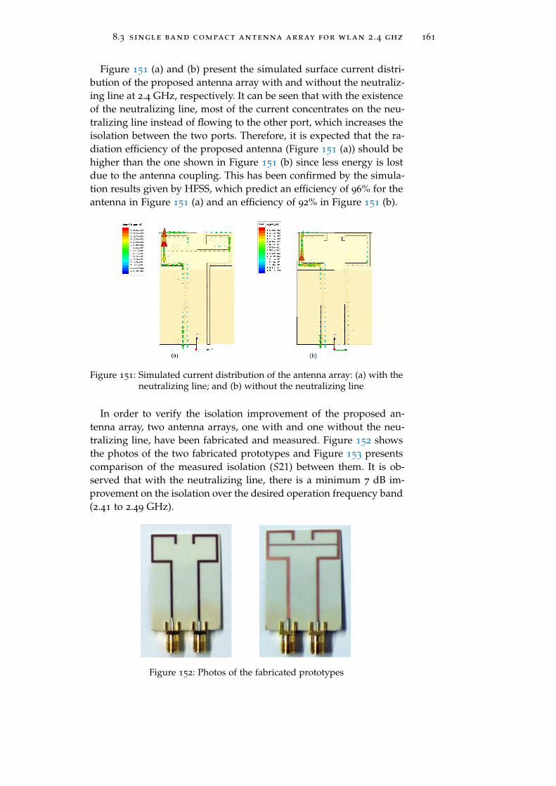
8.3 single band compact antenna array for wlan 2 .4 ghz 161
Figure 151 (a) and (b) present the simulated surface current distri-bution of the proposed antenna array with and without the neutraliz-ing line at 2.4 GHz, respectively. It can be seen that with the existenceof the neutralizing line, most of the current concentrates on the neu-tralizing line instead of flowing to the other port, which increases theisolation between the two ports. Therefore, it is expected that the ra-diation efficiency of the proposed antenna (Figure 151 (a)) should behigher than the one shown in Figure 151 (b) since less energy is lostdue to the antenna coupling. This has been confirmed by the simula-tion results given by HFSS, which predict an efficiency of 96% for theantenna in Figure 151 (a) and an efficiency of 92% in Figure 151 (b).
Figure 151: Simulated current distribution of the antenna array: (a) with theneutralizing line; and (b) without the neutralizing line
In order to verify the isolation improvement of the proposed an-tenna array, two antenna arrays, one with and one without the neu-tralizing line, have been fabricated and measured. Figure 152 showsthe photos of the two fabricated prototypes and Figure 153 presentscomparison of the measured isolation (S21) between them. It is ob-served that with the neutralizing line, there is a minimum 7 dB im-provement on the isolation over the desired operation frequency band(2.41 to 2.49 GHz).
Figure 152: Photos of the fabricated prototypes
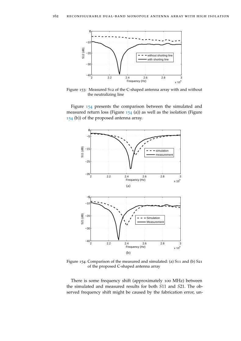
162 reconfigurable dual-band monopole antenna array with high isolation
2 2.2 2.4 2.6 2.8 3
x 109
−40
−30
−20
−10
00
Frequency (Hz)S
12 (
dB)
without shorting linewith shorting line
Figure 153: Measured S12 of the C-shaped antenna array with and withoutthe neutralizing line
Figure 154 presents the comparison between the simulated andmeasured return loss (Figure 154 (a)) as well as the isolation (Figure154 (b)) of the proposed antenna array.
2 2.2 2.4 2.6 2.8 3
x 109
−35
−25
−15
−5
00
Frequency (Hz)
S11
(dB
)
simulationmeasurement
(a)
2 2.2 2.4 2.6 2.8 3
x 109
−40
−30
−20
−10
−5−5
Frequency (Hz)
S21
(dB
)
SimulationMeasurement
(b)
Figure 154: Comparison of the measured and simulated: (a) S11 and (b) S21
of the proposed C-shaped antenna array
There is some frequency shift (approximately 100 MHz) betweenthe simulated and measured results for both S11 and S21. The ob-served frequency shift might be caused by the fabrication error, un-
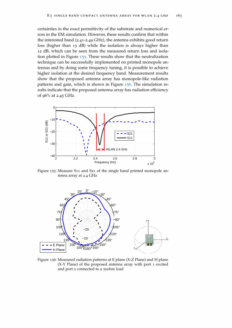
8.3 single band compact antenna array for wlan 2 .4 ghz 163
certainties in the exact permittivity of the substrate and numerical er-rors in the EM simulation. However, these results confirm that withinthe interested band (2.41-2.49 GHz), the antenna exhibits good returnloss (higher than 15 dB) while the isolation is always higher than12 dB, which can be seen from the measured return loss and isola-tion plotted in Figure 155. These results show that the neutralizationtechnique can be successfully implemented on printed monopole an-tennas and by doing some frequency tuning, it is possible to achievehigher isolation at the desired frequency band. Measurement resultsshow that the proposed antenna array has monopole-like radiationpatterns and gain, which is shown in Figure 156. The simulation re-sults indicate that the proposed antenna array has radiation efficiencyof 96% at 2.45 GHz.
2 2.2 2.4 2.6 2.8 3
x 109
−40
−30
−20
−10
0
Frequency (Hz)
S11
or
S21
(dB
)
S21S11
WLAN 2.4 GHz
Figure 155: Measure S11 and S21 of the single band printed monopole an-tenna array at 2.4 GHz
0°15°30°
45°
60°
75°
90°
105°
120°
135°150°
165°±180°−165°−150°
−135°
−120°
−105°
−90°
−75°
−60°
−45°−30°
−15°
−20
−10
0
E PlaneH Plane
Figure 156: Measured radiation patterns at E plane (X-Z Plane) and H plane(X-Y Plane) of the proposed antenna array with port 1 excitedand port 2 connected to a 50ohm load
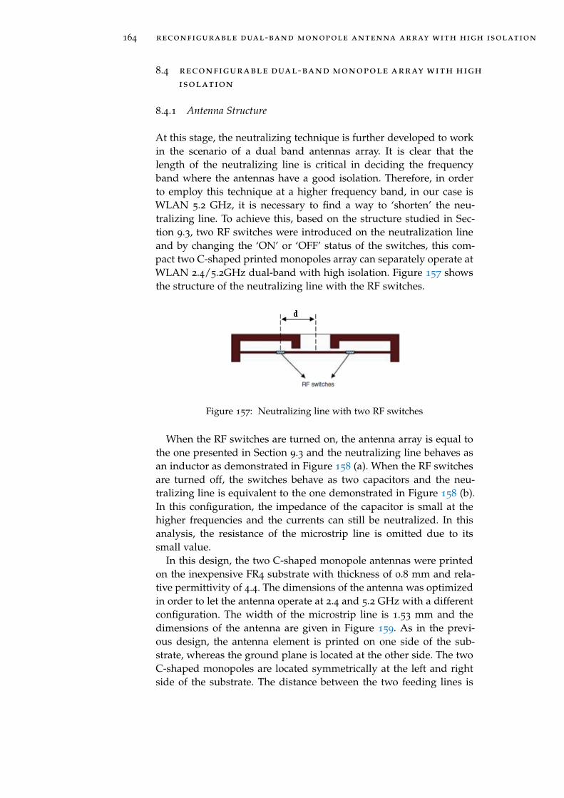
164 reconfigurable dual-band monopole antenna array with high isolation
8.4 reconfigurable dual-band monopole array with high
isolation
8.4.1 Antenna Structure
At this stage, the neutralizing technique is further developed to workin the scenario of a dual band antennas array. It is clear that thelength of the neutralizing line is critical in deciding the frequencyband where the antennas have a good isolation. Therefore, in orderto employ this technique at a higher frequency band, in our case isWLAN 5.2 GHz, it is necessary to find a way to ‘shorten’ the neu-tralizing line. To achieve this, based on the structure studied in Sec-tion 9.3, two RF switches were introduced on the neutralization lineand by changing the ‘ON’ or ‘OFF’ status of the switches, this com-pact two C-shaped printed monopoles array can separately operate atWLAN 2.4/5.2GHz dual-band with high isolation. Figure 157 showsthe structure of the neutralizing line with the RF switches.
Figure 157: Neutralizing line with two RF switches
When the RF switches are turned on, the antenna array is equal tothe one presented in Section 9.3 and the neutralizing line behaves asan inductor as demonstrated in Figure 158 (a). When the RF switchesare turned off, the switches behave as two capacitors and the neu-tralizing line is equivalent to the one demonstrated in Figure 158 (b).In this configuration, the impedance of the capacitor is small at thehigher frequencies and the currents can still be neutralized. In thisanalysis, the resistance of the microstrip line is omitted due to itssmall value.
In this design, the two C-shaped monopole antennas were printedon the inexpensive FR4 substrate with thickness of 0.8 mm and rela-tive permittivity of 4.4. The dimensions of the antenna was optimizedin order to let the antenna operate at 2.4 and 5.2 GHz with a differentconfiguration. The width of the microstrip line is 1.53 mm and thedimensions of the antenna are given in Figure 159. As in the previ-ous design, the antenna element is printed on one side of the sub-strate, whereas the ground plane is located at the other side. The twoC-shaped monopoles are located symmetrically at the left and rightside of the substrate. The distance between the two feeding lines is
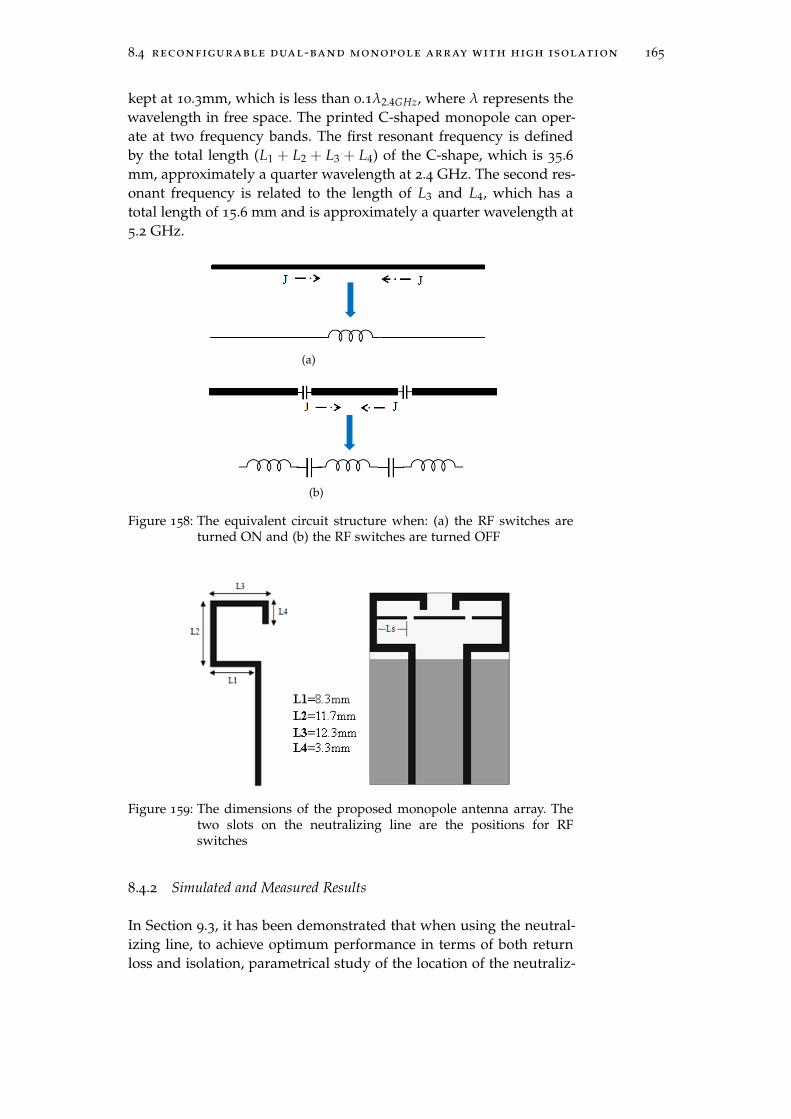
8.4 reconfigurable dual-band monopole array with high isolation 165
kept at 10.3mm, which is less than 0.1λ2.4GHz, where λ represents thewavelength in free space. The printed C-shaped monopole can oper-ate at two frequency bands. The first resonant frequency is definedby the total length (L1 + L2 + L3 + L4) of the C-shape, which is 35.6mm, approximately a quarter wavelength at 2.4 GHz. The second res-onant frequency is related to the length of L3 and L4, which has atotal length of 15.6 mm and is approximately a quarter wavelength at5.2 GHz.
(a)
(b)
Figure 158: The equivalent circuit structure when: (a) the RF switches areturned ON and (b) the RF switches are turned OFF
Figure 159: The dimensions of the proposed monopole antenna array. Thetwo slots on the neutralizing line are the positions for RFswitches
8.4.2 Simulated and Measured Results
In Section 9.3, it has been demonstrated that when using the neutral-izing line, to achieve optimum performance in terms of both returnloss and isolation, parametrical study of the location of the neutraliz-
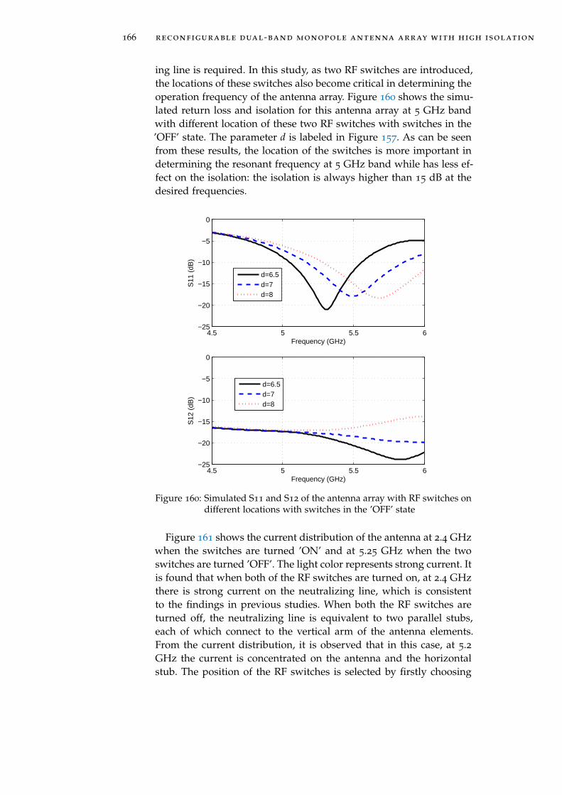
166 reconfigurable dual-band monopole antenna array with high isolation
ing line is required. In this study, as two RF switches are introduced,the locations of these switches also become critical in determining theoperation frequency of the antenna array. Figure 160 shows the simu-lated return loss and isolation for this antenna array at 5 GHz bandwith different location of these two RF switches with switches in the’OFF’ state. The parameter d is labeled in Figure 157. As can be seenfrom these results, the location of the switches is more important indetermining the resonant frequency at 5 GHz band while has less ef-fect on the isolation: the isolation is always higher than 15 dB at thedesired frequencies.
4.5 5 5.5 6−25
−20
−15
−10
−5
0
Frequency (GHz)
S11
(dB
)
d=6.5d=7d=8
4.5 5 5.5 6−25
−20
−15
−10
−5
0
Frequency (GHz)
S12
(dB
)
d=6.5d=7d=8
Figure 160: Simulated S11 and S12 of the antenna array with RF switches ondifferent locations with switches in the ’OFF’ state
Figure 161 shows the current distribution of the antenna at 2.4 GHzwhen the switches are turned ’ON’ and at 5.25 GHz when the twoswitches are turned ’OFF’. The light color represents strong current. Itis found that when both of the RF switches are turned on, at 2.4 GHzthere is strong current on the neutralizing line, which is consistentto the findings in previous studies. When both the RF switches areturned off, the neutralizing line is equivalent to two parallel stubs,each of which connect to the vertical arm of the antenna elements.From the current distribution, it is observed that in this case, at 5.2GHz the current is concentrated on the antenna and the horizontalstub. The position of the RF switches is selected by firstly choosing
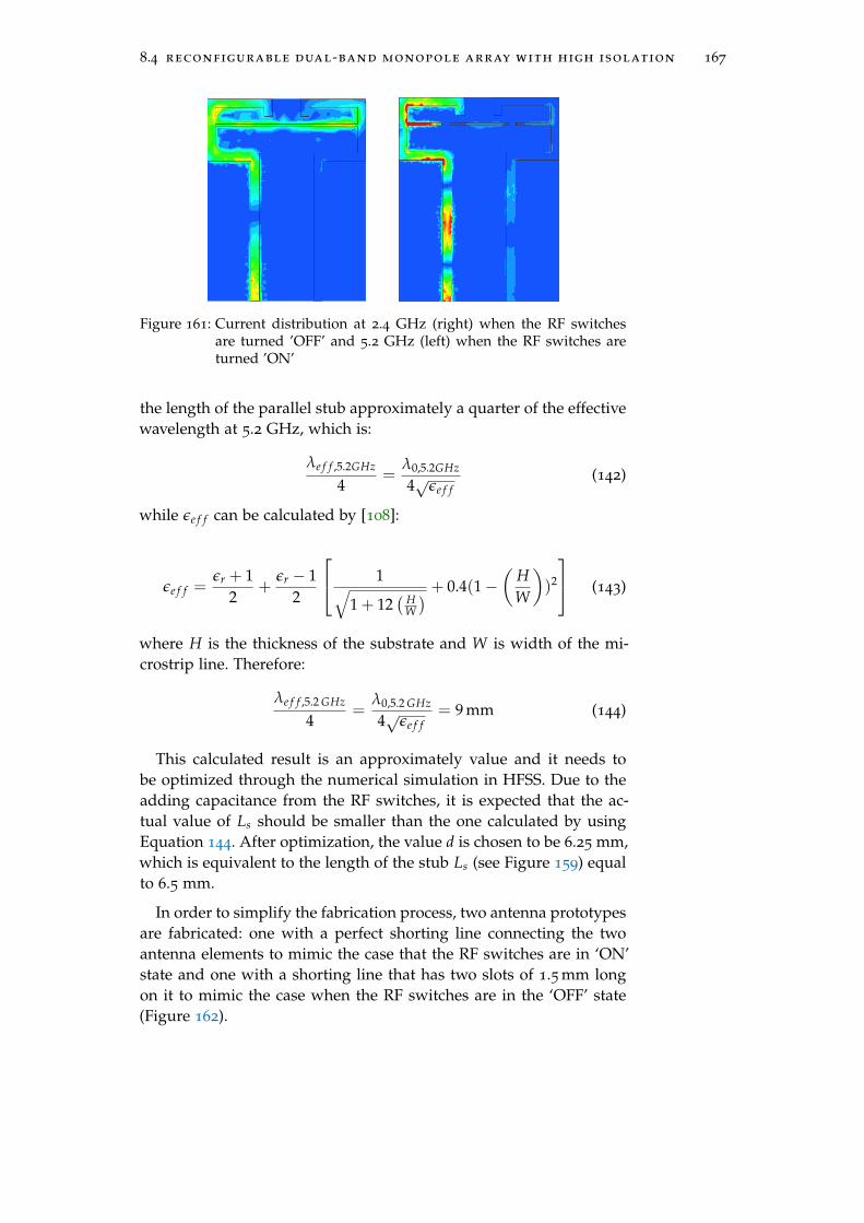
8.4 reconfigurable dual-band monopole array with high isolation 167
Figure 161: Current distribution at 2.4 GHz (right) when the RF switchesare turned ’OFF’ and 5.2 GHz (left) when the RF switches areturned ’ON’
the length of the parallel stub approximately a quarter of the effectivewavelength at 5.2 GHz, which is:
λe f f ,5.2GHz
4=
λ0,5.2GHz
4√εe f f(142)
while εe f f can be calculated by [108]:
εe f f =εr + 1
2+
εr − 12
1√1 + 12
( HW
) + 0.4(1−(
HW
))2
(143)
where H is the thickness of the substrate and W is width of the mi-crostrip line. Therefore:
λe f f ,5.2 GHz
4=
λ0,5.2 GHz
4√εe f f= 9 mm (144)
This calculated result is an approximately value and it needs tobe optimized through the numerical simulation in HFSS. Due to theadding capacitance from the RF switches, it is expected that the ac-tual value of Ls should be smaller than the one calculated by usingEquation 144. After optimization, the value d is chosen to be 6.25 mm,which is equivalent to the length of the stub Ls (see Figure 159) equalto 6.5 mm.
In order to simplify the fabrication process, two antenna prototypesare fabricated: one with a perfect shorting line connecting the twoantenna elements to mimic the case that the RF switches are in ‘ON’state and one with a shorting line that has two slots of 1.5 mm longon it to mimic the case when the RF switches are in the ‘OFF’ state(Figure 162).
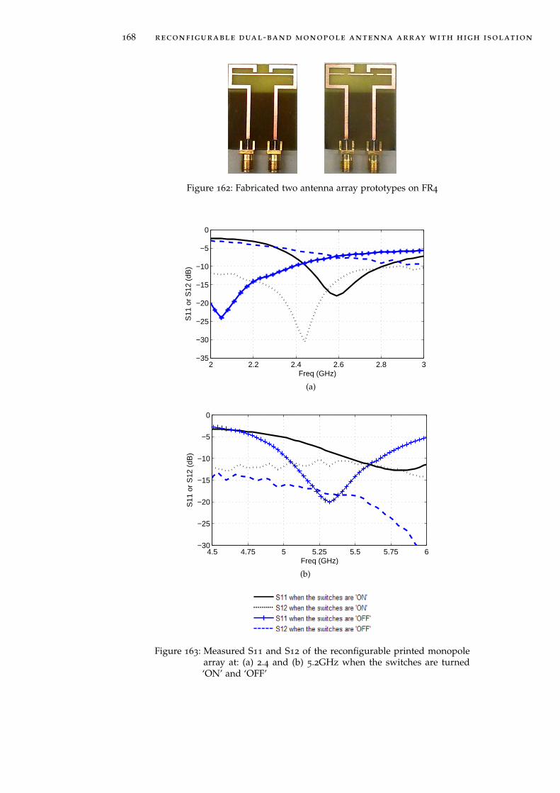
168 reconfigurable dual-band monopole antenna array with high isolation
Figure 162: Fabricated two antenna array prototypes on FR4
2 2.2 2.4 2.6 2.8 3−35
−30
−25
−20
−15
−10
−5
0
Freq (GHz)
S11
or
S12
(dB
)
(a)
4.5 4.75 5 5.25 5.5 5.75 6−30
−25
−20
−15
−10
−5
0
Freq (GHz)
S11
or
S12
(dB
)
(b)
Figure 163: Measured S11 and S12 of the reconfigurable printed monopolearray at: (a) 2.4 and (b) 5.2GHz when the switches are turned‘ON’ and ‘OFF’
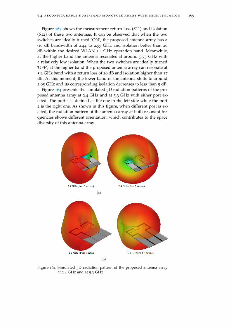
8.4 reconfigurable dual-band monopole array with high isolation 169
Figure 163 shows the measurement return loss (S11) and isolation(S12) of these two antennas. It can be observed that when the twoswitches are ideally turned ‘ON’, the proposed antenna array has a-10 dB bandwidth of 2.44 to 2.55 GHz and isolation better than 20
dB within the desired WLAN 2.4 GHz operation band. Meanwhile,at the higher band the antenna resonates at around 5.75 GHz witha relatively low isolation. When the two switches are ideally turned‘OFF’, at the higher band the proposed antenna array can resonate at5.2 GHz band with a return loss of 20 dB and isolation higher than 17
dB. At this moment, the lower band of the antenna shifts to around2.05 GHz and its corresponding isolation decreases to less than 5 dB.
Figure 164 presents the simulated 3D radiation patterns of the pro-posed antenna array at 2.4 GHz and at 5.3 GHz with either port ex-cited. The port 1 is defined as the one in the left side while the port2 is the right one. As shown in this figure, when different port is ex-cited, the radiation pattern of the antenna array at both resonant fre-quencies shows different orientation, which contributes to the spacediversity of this antenna array.
(a)
(b)
Figure 164: Simulated 3D radiation pattern of the proposed antenna arrayat 2.4 GHz and at 5.3 GHz
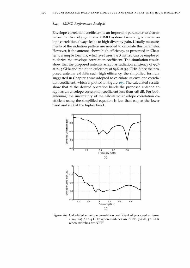
170 reconfigurable dual-band monopole antenna array with high isolation
8.4.3 MIMO Performance Analysis
Envelope correlation coefficient is an important parameter to charac-terize the diversity gain of a MIMO system. Generally, a low enve-lope correlation always leads to high diversity gain. Usually measure-ments of the radiation pattern are needed to calculate this parameter.However, if the antenna shows high efficiency, as presented in Chap-ter 7, a simple formula, which just uses the S matrix, can be employedto derive the envelope correlation coefficient. The simulation resultsshow that the proposed antenna array has radiation efficiency of 95%at 2.45 GHz and radiation efficiency of 89% at 5.3 GHz. Since the pro-posed antenna exhibits such high efficiency, the simplified formulasuggested in Chapter 7 was adopted to calculate its envelope correla-tion coefficient, which is plotted in Figure 165. The calculated resultsshow that at the desired operation bands the proposed antenna ar-ray has an envelope correlation coefficient less than -28 dB. For bothantennas, the uncertainty of the calculated envelope correlation co-efficient using the simplified equation is less than 0.05 at the lowerband and 0.12 at the higher band.
2 2.2 2.4 2.6 2.8 3−80
−60
−40
−20
0
Frequency (GHz)
Env
elop
e C
orre
latio
n (d
B)
(a)
4.6 4.8 5 5.2 5.4 5.6−40
−30
−20
−10
0
Frequency(GHz)
Env
elop
e C
orre
latio
n (d
B)
(b)
Figure 165: Calculated envelope correlation coefficient of proposed antennaarray: (a) At 2.4 GHz when switches are ‘ON’; (b) At 5.2 GHzwhen switches are ‘OFF’
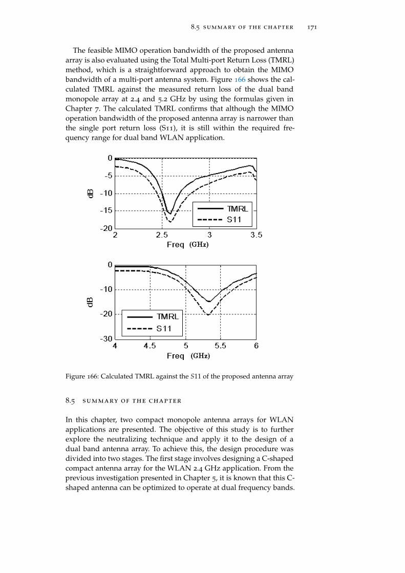
8.5 summary of the chapter 171
The feasible MIMO operation bandwidth of the proposed antennaarray is also evaluated using the Total Multi-port Return Loss (TMRL)method, which is a straightforward approach to obtain the MIMObandwidth of a multi-port antenna system. Figure 166 shows the cal-culated TMRL against the measured return loss of the dual bandmonopole array at 2.4 and 5.2 GHz by using the formulas given inChapter 7. The calculated TMRL confirms that although the MIMOoperation bandwidth of the proposed antenna array is narrower thanthe single port return loss (S11), it is still within the required fre-quency range for dual band WLAN application.
Figure 166: Calculated TMRL against the S11 of the proposed antenna array
8.5 summary of the chapter
In this chapter, two compact monopole antenna arrays for WLANapplications are presented. The objective of this study is to furtherexplore the neutralizing technique and apply it to the design of adual band antenna array. To achieve this, the design procedure wasdivided into two stages. The first stage involves designing a C-shapedcompact antenna array for the WLAN 2.4 GHz application. From theprevious investigation presented in Chapter 5, it is known that this C-shaped antenna can be optimized to operate at dual frequency bands.

172 reconfigurable dual-band monopole antenna array with high isolation
Therefore, the task for the second stage turns to investigate possiblesolutions to extend the neutralization technique to operate at dual fre-quency bands. The methodology employed to achieve high isolationat two frequency bands is to implement a reconfigurable neutralizingline: two RF switches were introduced on the neutralizing line. Bychanging the states of these two switches, the antenna array can re-spectively operate whist exhibit high isolation at each of the WLANdual frequency band. Experimental results show that the proposedantenna can operate either at 2.4 or 5.2 GHz bands with isolationhigher than 17 dB over the entire frequency bands of interest. More-over, this antenna array also shows low envelope correlation at therequired frequency bands, which leads to a good diversity gain. Thefeasible operational bandwidth of this MIMO antenna array was alsoanalyzed using the TMRL method, which agrees well with the analy-sis using the envelope correlation coefficient.
The following is the list of publications resulted from the workpresented in this chapter:
1. Qi Luo; H. M. Salgado and J. R. Pereira. Compact Printed MonopoleAntenna Array for Dual Band WLAN Application. In Proceed-ings of International Conference on Computer as a Tool (EUROCON),Lisbon, Portugal, November 2011.
2. Q. Luo; H.M. Salgado and J.R. Pereira. Printed C-shaped MonopoleAntenna Array With High Isolation For MIMO Applications. InProceedings of IEEE Antennas and Propagation Society InternationalSymposium, Toronto, Canada, July 2010.
3. Q. Luo; J.R. Pereira and H.M. Salgado. Reconfigurable dualband C-shaped monopole antenna array with high isolation.Electronics Letters, 46(13):888-889, June 2010.
9C O N C L U S I O N A N D F U T U R E W O R K
9.1 conclusion
The main objective of this thesis work is to address the miniaturiza-tion of multi-frequency microstrip antennas and antenna arrays in thecontext of high data rate wireless communication. The size of one res-onant antenna as well as the distance between each antenna elementin an antenna array is proportional to its wavelength. As a result, thesize reduction of the antenna or antenna array will inevitably lead tothe lowering of the radiation performance of the antenna or antennaarray. Therefore, it is always a trade-off between the volume of theantenna and its radiation properties.
The fundamental limitation established by Wheeler and Chu givesa clear guideline for the antenna design: the antenna can be designedto approach this limit but can never be smaller than that. The sizereduction of the antennas that were presented in this thesis workis achieved by using fractal geometries or introducing lumped el-ements into the antenna radiation elements. The new designs pre-sented are three multiband fractal monopole antennas, one fractal-based Inverted-L antenna (ILA) and one single feed fractal monopoleantenna array. Moreover, two electrically small antennas for dual bandWLAN and one compact antenna for multiband mobile communica-tion that can cover almost the entire commercial available frequencybands (GSM, PCS, UMTS, WLAN and WiMAX) are also presented.The applications of these designs include PC card, USB dongles andmobile devices. The experiment and simulation results prove the ef-fectiveness of the proposed methods in the aspect of antenna sizereduction and multi-frequency operation.
The compact multiband antenna array was designed by furtherinvestigating the neutralization and employing reconfigurable tech-niques. The new designs presented in this thesis work include twocompact size single band antenna arrays for the WLAN 2.4 GHz andWLAN 5.8 GHz application and one compact dual band compactmonopole antennas array for dual band WLAN applications (2.4/5.2GHz). In these designs, the antennas are closely spaced (less than1/10th of the wavelength) and the antenna array proposed for theWLAN 5.8 GHz is compact enough to be included in a USB dongle.Another novel work is the design of a reconfigurable antenna basedon the concept of active Artificial Magnetic Conductor ground plane.In this proposed antenna, the resonant frequency of the coplanar an-tenna can be reconfigured by using an active AMC ground plane
173
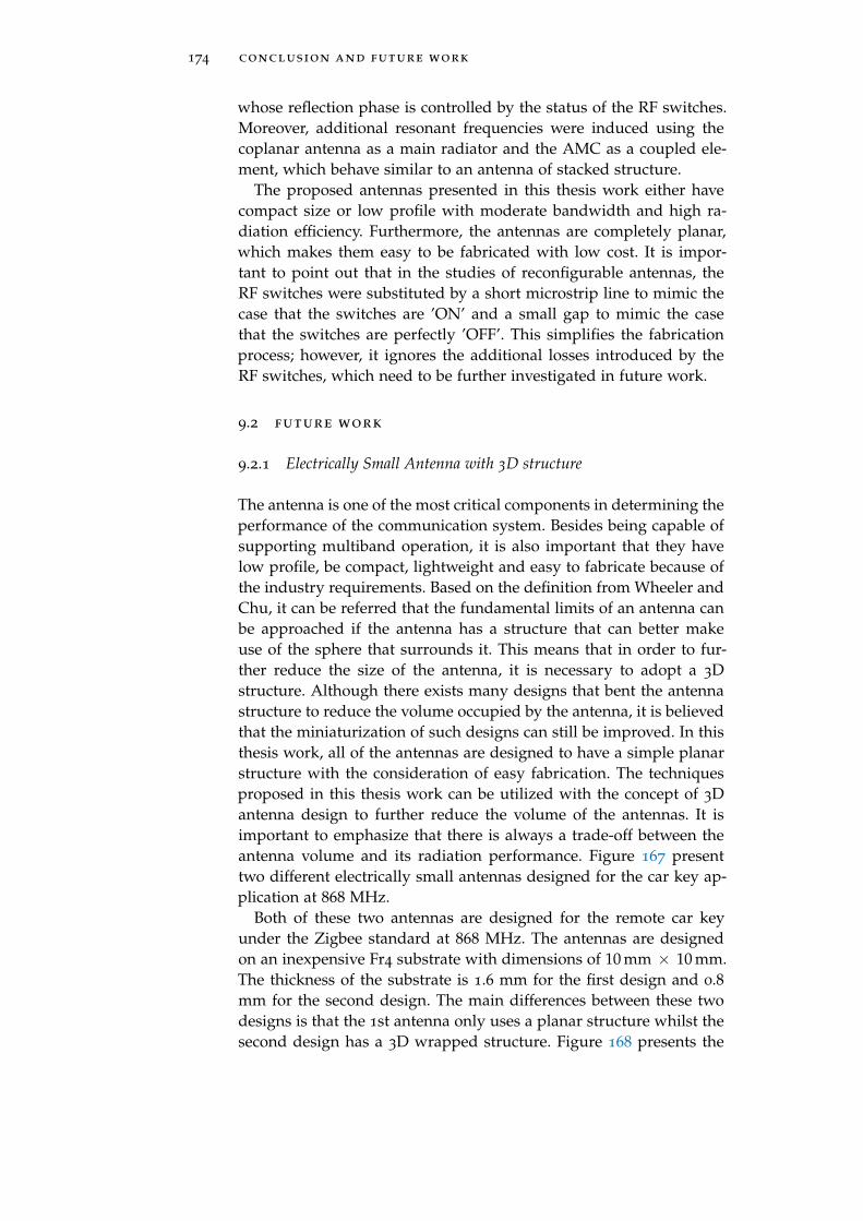
174 conclusion and future work
whose reflection phase is controlled by the status of the RF switches.Moreover, additional resonant frequencies were induced using thecoplanar antenna as a main radiator and the AMC as a coupled ele-ment, which behave similar to an antenna of stacked structure.
The proposed antennas presented in this thesis work either havecompact size or low profile with moderate bandwidth and high ra-diation efficiency. Furthermore, the antennas are completely planar,which makes them easy to be fabricated with low cost. It is impor-tant to point out that in the studies of reconfigurable antennas, theRF switches were substituted by a short microstrip line to mimic thecase that the switches are ’ON’ and a small gap to mimic the casethat the switches are perfectly ’OFF’. This simplifies the fabricationprocess; however, it ignores the additional losses introduced by theRF switches, which need to be further investigated in future work.
9.2 future work
9.2.1 Electrically Small Antenna with 3D structure
The antenna is one of the most critical components in determining theperformance of the communication system. Besides being capable ofsupporting multiband operation, it is also important that they havelow profile, be compact, lightweight and easy to fabricate because ofthe industry requirements. Based on the definition from Wheeler andChu, it can be referred that the fundamental limits of an antenna canbe approached if the antenna has a structure that can better makeuse of the sphere that surrounds it. This means that in order to fur-ther reduce the size of the antenna, it is necessary to adopt a 3Dstructure. Although there exists many designs that bent the antennastructure to reduce the volume occupied by the antenna, it is believedthat the miniaturization of such designs can still be improved. In thisthesis work, all of the antennas are designed to have a simple planarstructure with the consideration of easy fabrication. The techniquesproposed in this thesis work can be utilized with the concept of 3Dantenna design to further reduce the volume of the antennas. It isimportant to emphasize that there is always a trade-off between theantenna volume and its radiation performance. Figure 167 presenttwo different electrically small antennas designed for the car key ap-plication at 868 MHz.
Both of these two antennas are designed for the remote car keyunder the Zigbee standard at 868 MHz. The antennas are designedon an inexpensive Fr4 substrate with dimensions of 10 mm × 10 mm.The thickness of the substrate is 1.6 mm for the first design and 0.8mm for the second design. The main differences between these twodesigns is that the 1st antenna only uses a planar structure whilst thesecond design has a 3D wrapped structure. Figure 168 presents the
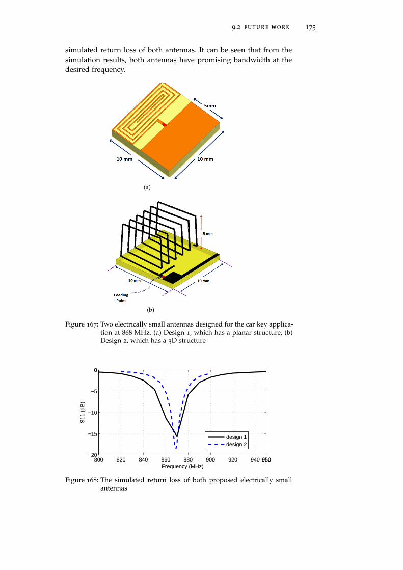
9.2 future work 175
simulated return loss of both antennas. It can be seen that from thesimulation results, both antennas have promising bandwidth at thedesired frequency.
(a)
(b)
Figure 167: Two electrically small antennas designed for the car key applica-tion at 868 MHz. (a) Design 1, which has a planar structure; (b)Design 2, which has a 3D structure
800 820 840 860 880 900 920 940 950950−20
−15
−10
−5
00
Frequency (MHz)
S11
(dB
)
design 1design 2
Figure 168: The simulated return loss of both proposed electrically smallantennas
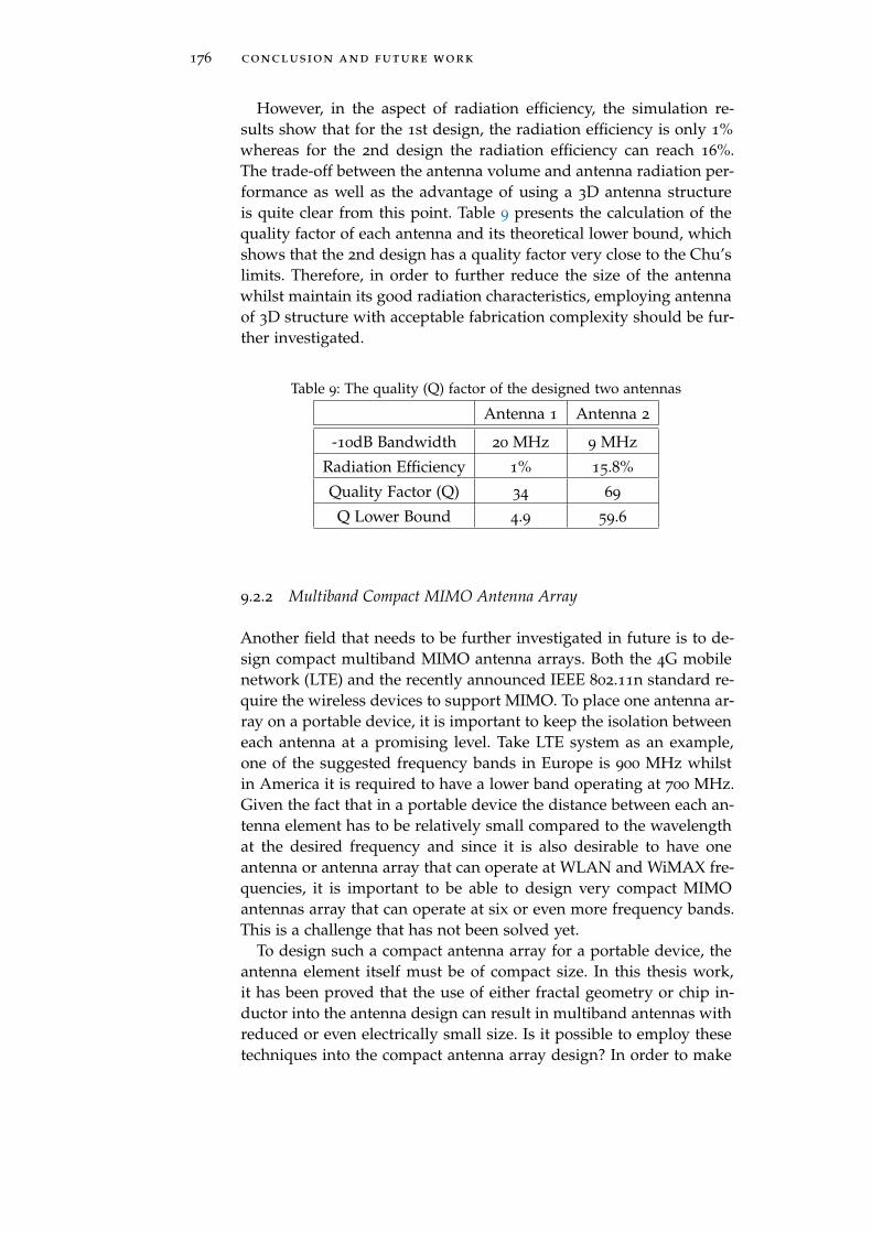
176 conclusion and future work
However, in the aspect of radiation efficiency, the simulation re-sults show that for the 1st design, the radiation efficiency is only 1%whereas for the 2nd design the radiation efficiency can reach 16%.The trade-off between the antenna volume and antenna radiation per-formance as well as the advantage of using a 3D antenna structureis quite clear from this point. Table 9 presents the calculation of thequality factor of each antenna and its theoretical lower bound, whichshows that the 2nd design has a quality factor very close to the Chu’slimits. Therefore, in order to further reduce the size of the antennawhilst maintain its good radiation characteristics, employing antennaof 3D structure with acceptable fabrication complexity should be fur-ther investigated.
Table 9: The quality (Q) factor of the designed two antennas
Antenna 1 Antenna 2
-10dB Bandwidth 20 MHz 9 MHz
Radiation Efficiency 1% 15.8%
Quality Factor (Q) 34 69
Q Lower Bound 4.9 59.6
9.2.2 Multiband Compact MIMO Antenna Array
Another field that needs to be further investigated in future is to de-sign compact multiband MIMO antenna arrays. Both the 4G mobilenetwork (LTE) and the recently announced IEEE 802.11n standard re-quire the wireless devices to support MIMO. To place one antenna ar-ray on a portable device, it is important to keep the isolation betweeneach antenna at a promising level. Take LTE system as an example,one of the suggested frequency bands in Europe is 900 MHz whilstin America it is required to have a lower band operating at 700 MHz.Given the fact that in a portable device the distance between each an-tenna element has to be relatively small compared to the wavelengthat the desired frequency and since it is also desirable to have oneantenna or antenna array that can operate at WLAN and WiMAX fre-quencies, it is important to be able to design very compact MIMOantennas array that can operate at six or even more frequency bands.This is a challenge that has not been solved yet.
To design such a compact antenna array for a portable device, theantenna element itself must be of compact size. In this thesis work,it has been proved that the use of either fractal geometry or chip in-ductor into the antenna design can result in multiband antennas withreduced or even electrically small size. Is it possible to employ thesetechniques into the compact antenna array design? In order to make

9.2 future work 177
use of the available volume, it is necessary to ‘wrap’ the antennas toobtain a three-dimensional structure. As a result, it is necessary to as-sess the impact of bending the radiation element on a normal planarfractal antenna. Another solution that can be introduced into the an-tenna array design is to embed the chip inductors on the single radia-tion element, which has been studied in this thesis work and provedto be an effective method to reduce the size of one single antenna.With respect to improve the isolation between each antenna, espe-cially at multiple frequency bands, more innovative techniques are re-quired. It is shown that introducing the reconfigurable method to theneutralizing technique, a compact dual band antenna array with highisolation can be implemented. Is it possible to achieve high isolationat three or even more frequency bands by adding extra RF switcheson the radiation element, feeding line or ground plane besides on theneutralizing line? Under this configuration, one frequency tunableantenna with a reconfigurable neutralizing line might be achieved af-ter suitable optimization, including the location of the RF Switches,lumped elements and the input impedance matching at multiple res-onant frequencies. This is one direction that is worth exploring boththeoretically and experimentally.
To the date of writing this thesis, one of the first published designsof the multiband antenna array for LTE applications was presentedin [109]. In that design, both antennas were located at the bottom ofthe PCB board and the distance between antennas is relatively smallcompared to the lowest resonant frequency, which is 700 MHz forLTE standard. There are two things needed to be highlight in this de-sign. Firstly, the size reduction of both of the antennas were achievedby wrapping the resonant element to form a 3D structure and em-bedding one chip inductor on the antenna to induce the lowest res-onant frequency. Secondly, the high isolation between the antennaswas reached by adding one protruded ground plane. The results pro-vided in [109] show that the proposed antenna array can performLTE MIMO operation in the LTE700/ 2300/2500 bands. Althoughthat this antenna array does not cover all the required LTE bands, itshows clearly that to achieve a compact multiband antenna array, dif-ferent antenna and antenna array miniaturization techniques need tobe implemented simultaneously.
Metamaterial inspired antenna is another interesting field that worthinvestigating further. Electromagnetic band gap (EBG) material andartificial magnetic conductor (AMC) have already been widely em-ployed in the low profile antenna design with increased radiationperformance. However, the use of periodic structures will lead toa relatively large overall volume, which is not suitable for antennaminiaturization. Therefore, future trends of using such artificial ma-terials into the compact antenna design should employ less or sin-gle metamaterial cells to design double negative (DNG) zeroth order

178 conclusion and future work
resonator (ZOR), a subject which have attracted much research in-terest. Theoretically the size of one antenna designed using ZOR isnot proportional to its corresponding wavelength, which can be ad-vantageous to design antennas for low frequencies applications. Itis also known that metamaterial can also be employed to suppressthe propagation of surface waves, which is one of the first applica-tions of such artificial materials. Then, using metamaterial inspiredantenna to design compact antenna array with high isolation becomesanother possible approach. The surface wave suppressing brought bythe metamaterials has been widely studied; however, the operationof the metamaterial inspired antenna is still not well understood andrequires to be further investigated. One key issue for the design ofmetamaterial inspired antenna array is how to make the operationalfrequency band of the antenna and surface wave suppressing band ofthe metamaterial to be within the same frequency region. One morechallenge is that, looking at the existing publications, it is found thatthe metamaterial inspired antenna reported to date have a relativelynarrow bandwidth, which needs to be improved in future work.

B I B L I O G R A P H Y
[1] Qualcomm: http://qualcomm.com/technology, Retrieved 30 August2011. (Cited on page 1.)
[2] Motorola. Long Term Evolution (LTE). Technical report, Re-trieved 12 August 2011. (Cited on page 2.)
[3] IEEE-SA. IEEE 802.11n-2009-Amendment 5: Enhancements forHigher Throughput. Technical report, 2009. (Cited on page 2.)
[4] Ke-Lin Du and M. N. S. Swamy. Wireless Communication Systems:From RF Subsystems to 4G Enabling Technologies. Cambridge Uni-versity Press, 2010. (Cited on page 3.)
[5] B.B.Mandelbrot. The Fractal Geometry of Nature.N.Y.W.H.Freeman, 1983. (Cited on page 3.)
[6] D.H.Werner and S.Ganduly. An Overview Of Fractal AntennaEngineering Research. IEEE Antennas and Propagation Magazine,45(1):38–57, 2003. (Cited on pages 3 and 51.)
[7] G.G.Chavka. Beauty Of Fractals, Design Of Fractal Antennas.In Proceedings of International Conference on Antenna Theory andTechniques, 2007. (Cited on page 3.)
[8] R. Mitrra. A Critical Look At The Problem Of Small AntennaDesign And A Review Of Physics-Based Performance Limita-tions Of These Antenna. In Proceedings of Loughborough Antennasand Propagation Conference, UK, March 2008. (Cited on page 3.)
[9] J.P.Gianvittorio and Y.Rahmat-Samii. Fractal Antennas: ANovel Antenna Miniaturization Techniques, And Applications.IEEE Antennas and Propagation Magazine, 44(1):20–36, 2002.(Cited on pages 3 and 51.)
[10] Gerald Edgar. Measure, Topology, and Fractal Geometry (2nd Edi-tion). Springer Science, 2008. (Cited on pages 4 and 42.)
[11] O.Q.Teruel; E.Pucci and E.R.Iglesias. Compact Loaded PIFA forMultifrequency Application. IEEE Transactions on Antennas andPropagation, 58(3):656–664, 2010. (Cited on pages 4 and 92.)
[12] B.R.Holland; R.Ramadoss; S.Pandey and P.Agrawal. Tun-able coplanar patch antenna using varactor. Electronic Letters,42(6):319–321, 2006. (Cited on pages 4 and 6.)
179

180 bibliography
[13] K.Wong and S.Chen. Printed Single-Strip Monopole UsingA Chip Inductor For Penta-Band WWAN Operation In TheMobile Phone. IEEE Transactions on Antennas and Propagation,58(3):1011–1014, 2010. (Cited on pages 4, 92, and 112.)
[14] T. Kang and K.Wong. Chip-Inductor-Embedded Small-SizePrinted Strip Monopole For WWAN Operation In The MobilePhone. Microwave and Optical Technology Letter, 51(4):966–971,2009. (Cited on pages 4 and 92.)
[15] F.Yang and Y. Rahmat-Samii. Microstrip Antennas IntegratedWith Electromagnetic Band-Gap (EBG) Structures: A Low Mu-tual Coupling Design for Array Applications. IEEE Transactionson Antennas and Propagation, 51(10):2936–2946, 2003. (Cited onpages 5 and 158.)
[16] A. Tavakoli M. Salehi; A. Motevasselian and T. Heidari. MutualCoupling Reduction of Microstrip Antennas using DefectedGround Structure. In Proceeding of 10th IEEE Singapore Inter-national Conference on Communication systems, 2006. (Cited onpages 5 and 158.)
[17] C.Luxey. Design of Multi-Antenna Systems for UMTS MobilePhones. In Preceeding of Loughborough Antenna & PropagationConference, UK, 2009. (Cited on pages 5, 10, 129, 130, 131, 158,and 159.)
[18] A.Diallo; C.Luxey; P.L.Thu; R.Staraj and G.Kossiavas. Enhancedtwo-antenna structures for universal mobile telecommunica-tions system diversity terminals. IET Microwave and AntennaPropagation, 2(1):93–101, 2008. (Cited on page 5.)
[19] A. Diallo;C. Luxey; P. Le Thuc; R. Staraj and G. Kossiavas.Efficient two-port antenna system for GSM/DCS/UMTS mul-timode mobile phones. Electronic Letters, 43(7):369–370, 2007.(Cited on page 5.)
[20] A.S.; Gyubok Park; Minchan Kim; Taesik Yang; JoonhoByun; Kim. The compact quad-band mobile handset antennafor the LTE700 MIMO application. In Proceedings of IEEE Anten-nas and Propagation Society International Symposium, 2009. (Citedon page 5.)
[21] E. Del Re; S. Morosi; D. Marabissi; L. Mucchi; L. Pierucciand L. S. Ronga;. Reconfigurable Antenna for FutureWire-less Communication Systems. Wireless Personal Communications(Springer), 42:405–430, 2007. (Cited on page 6.)
[22] N.P. Cummings. Active Antenna Bandwidth Control Using recon-figurable antenna elements. PhD thesis, Faculty of the ViginiaPolytechnic Institure & State University, 2003. (Cited on page 6.)

bibliography 181
[23] D. Peroulis; K. Sarabandi and L. P. B. Katehi;. Design of Re-configurable Slot Antennas. IEEE Transactions on Antennas andPropagation, 53(2):645–654, 2005. (Cited on page 6.)
[24] F.Yang. EBG Structure and Reconfigurable Techniques in AntennaDesign: Application to Wireless Communications. PhD thesis, De-partment of Electrical Engineering, University of California,2003. (Cited on page 6.)
[25] V.K. Kunda and M. Ali;. Reconfigurable stacked patch antennafor satellite and terrestrial applications. In Proceedings of IEEETopical Conference on Wireless Communication Technology, pages152–153, 2003. (Cited on page 6.)
[26] S.Oh; J. T. Aberle; S. Anantharaman; K. Arai; H. L.Chong andS. C. Koay;. Electronically Tunable Antenna Pair and Novel RFFront-End Architecture for Software-Defined Radios. EURASIPJournal on Applied Signal Processing, 2005:2701–2707, 2005. (Citedon page 6.)
[27] G. Goussetis; A.P. Feresidis and J.C. Vardaxoglou;. Tailoringthe AMC and EBG Characteristics of Periodic Metallic ArraysPrinted on Grounded Dielectric Substrate. IEEE Transactions onAntennas and Propagation, 54(1):82–89, 2006. (Cited on page 7.)
[28] Dan Sievenpiper; Lijun Zhang; Romulo F. Jimenez Broas;Nicholas G. Alexopolous and Eli Yablonovitch;. High-Impedance Electromagnetic Surfaces with a Forbidden Fre-quency Band. IEEE Transactions on Antennas and Propagation,47(11):2059–2074, 1999. (Cited on page 7.)
[29] F.Costa; S.Talarico; A.Monorchio and M.F.Valeri. An activeAMC ground plane for tunable low-profile antennas. In Pro-ceeding of IEEE Antenna and Propagation Society international Sym-posium, 2008. (Cited on pages 7 and 147.)
[30] J.Liang and H.Y.D.Yang. Microstrip Patch Antenna on TunableElectromagnetic Band-Gap Substrate. IEEE Transactions on An-tennas and Propagation, 57(6):1612–1617, 2009. (Cited on pages 7
and 147.)
[31] D. H. Werner; D. J. Kern and M. G. Bray. Advances in EBGDesign Concepts Based on Planar FSS Structures. In Proceedingsof the Loughborough Antennas and Propagation Conference, 2005.(Cited on pages 7 and 147.)
[32] L.J.Rocha; M.Martinez-Vazquez and R.S.Calvo, editors. Hand-Book on Small Antennas (Special Draft Edition). Universitat Po-litecnica de Catalunya, Spain, 2011. (Cited on page 15.)

182 bibliography
[33] W.Yu; X.Yang; Y.Liu; Z.Li; R.Mittra; L.Li and N.Huang. Electro-magnetic Simulation Engineering. Pennsylvania State University,USA, 2010. (Cited on page 15.)
[34] D. Manteuffel. Numerical technique. Lecture notes for Eu-ropen Antenna School on Industry Antenna Design, April 2011.(Cited on page 15.)
[35] R. F. Harrington. Field computation by moment methods. Macmil-lan, 1968. (Cited on page 15.)
[36] K.Yee. Numerical solution of initial boundary value problemsinvolving maxwell’s equations in isotropic media. IEEE Trans-actions on Antennas and Propagation, 14:302–307, 1966. (Cited onpage 17.)
[37] P.P.Silvester. Finite elements solution of homogeneous waveg-uide problems. Alta Freq., 38:313–317, May 1969. (Cited onpage 21.)
[38] K.K.Mei. Unimoment method of solving antenna and scatteringproblems. IEEE Transactions on Antennas and Propagation, 22:760–766, November 1974. (Cited on page 21.)
[39] J.M.Jin. The finite element method in electromagnetics (2nd). JohnWiley & SONS, INC, 2002. (Cited on pages 21, 22, 30, 32,and 33.)
[40] A.C.Polycarpou. Introduction to the finite element method in elec-tromagnetics. Morgan & Claypool, 2006. (Cited on pages 22, 23,24, 25, and 28.)
[41] Hyochoong Bang Young W.Kwon. The Finite Element Methodusing MATLAB. CRC Press, 1997. (Cited on page 31.)
[42] Benoit B. Mandelbrot. The Fractal Geometry of Nature. W. H.Freeman and Company,New York, 1982. (Cited on page 41.)
[43] Kenneth Falconer. FRACTAL GEOMETRY:Mathematical Founda-tions and Applications(2nd Edition). John Wiley & Sons, 2003.(Cited on pages 41 and 44.)
[44] Stephen Demko. Construction of fractal objects with iteratedfunction systems. In SIGGRAPH ’85 Proceedings of the 12th an-nual conference on Computer graphics and interactive techniques, vol-ume 19, 1985. (Cited on page 43.)
[45] Ansoft. HFSS Scripting Guide: HFSS and VBScript, 2010. (Citedon page 46.)
[46] David M. Pozar. Microwave engineering. J. Wiley, 2005. (Citedon page 48.)

bibliography 183
[47] J Anguera; C Puente and J Soler. Miniature monopole antennabased on the fractal hilbert curve. IEEE Antennas and Propaga-tion Society International Symposium, 4:546–549, 2002. (Cited onpage 51.)
[48] G.F.Tsachtsiris; C.F.Soras; M.P.Karaboikis and V.T.Makios. Anal-ysis of a modified sierpinski gasket monopole antenna printedon dual band wireless devices. IEEE Transactions on Antennasand Propagation, 52(10):2571–2579, 2004. (Cited on page 51.)
[49] S.R.Best and J.D.Morrow. The effectiveness of space-filling frac-tal geometry in lowering resonant frequnency. IEEE Anten-nas and Wireless Propagation Letter, 1:112–115, 2002. (Cited onpages 51 and 85.)
[50] S.R.Best. A discussion on the significance of geometry in de-termining the resonant behaviour of fractal and other non-euclidean wire antennas. IEEE Antennas and Propagation Mag-azine, 45(3):9–28, 2003. (Cited on page 51.)
[51] W.C.Su and K.L.Wong. Internal pifas for umts/wlan/wimaxmulti-network for a usb dongle. Microwave and Optical Technol-ogy Letters, 48:2249–2253, 2006. (Cited on page 59.)
[52] C.C.Lin; S.W. Kuo and H.R. Chuang. A 2.4-ghz printedmeander-line antenna for usb wlan with notebook-pc housing.IEEE Microwave and Wireless Components Letters, 15(9):546–548,2005. (Cited on page 59.)
[53] Y. Song; Y.C.Jiao and ed. Compact printed monopole antennafor multiband wlan applications. Microwave and Optical Technol-ogy Letters, 50(2):365–367, 2008. (Cited on page 59.)
[54] N.Cohen. Fractal antenna applications in wireless telecommu-nications. In Electronics Industries Forum of New England, 1997.Professional Program Proceedings, pages 43 – 49, 1997. (Cited onpage 60.)
[55] R.R.Ramirez; F. De Flaviis; N.G.Alexopoules. Single feed cir-cularly polarized microstrip ring antenna aiid arrays. IEEETransactions on Antennas and Propagation, 48(7):1040 – 1047, 2000.(Cited on page 73.)
[56] A.E.Abdulhadi and A.R.Sebak. Single feed circularly polarizedmicrostrip antenna array. In 2nd International ITG Conference onAntennas, pages 162 – 165, 2007. (Cited on page 73.)
[57] T.Y.Wu; S.T.Fang and K.L.Wong. Printed monopole arrayantenna for wlan operation in the 2.4/5.2/5.8ghz bands.Microwave and Optical Technology Letters, 37(5):370–372, 2003.(Cited on page 73.)

184 bibliography
[58] Q. Luo; H. M. Salgado; J. R. Pereira. Fractal monopole antennadesign using minkowski island geometry. In IEEE InternationalSymposium on Antennas & Propagation Proceeding, 2009. (Citedon page 73.)
[59] C.Y.Pan; T.S.Horng; W.S.Chen and C.H.Huang. Dual widebandprinted monopole antenna for wlan/wimax applications. IEEEAntenna and Wireless Propagation Letters, 6:149–151, 2007. (Citedon pages 73 and 75.)
[60] M.John and M.J.Ammann. Wideband printed monopole designusing a genetic algorithm. IEEE Antenna and Wireless Propaga-tion Letters, 6:447–449, 2007. (Cited on page 73.)
[61] H.A.Wheeler. Fundamental limitations of small antennas. Pro-ceedings of the I.R.E., 35(12):1479–1484, December 1947. (Citedon pages 85 and 86.)
[62] R.B.Adler; L.J.Chu and R.M.Fano. Electromagnetic Energy Trans-mission and Radiation. New York: Wiley, 1960. (Cited onpage 85.)
[63] S.R.Best. Antenna Engineering Handbook. McGraw-Hill, fourthedition edition, 2007. (Cited on page 85.)
[64] L.J.Chu. Physical limitations of omni-directional antennas.J.Appl.Phys., 19:1163–1175, December 1948. (Cited on pages 86
and 87.)
[65] R.C.Hansen. Fundamental limitations in antennas. Proceedingsof the IEEE, 69(2):170–182, February 1981. (Cited on page 86.)
[66] J.S.McLean. A re-examination of the fundamental limits on theradiation q of electrically small antennas. IEEE Transactions onAntennas and Propagation, 44(5):672–676, May 1996. (Cited onpage 87.)
[67] A.D.Yaghjian and S.R.Best. Impedance, bandwidth, and qof antennas. IEEE Transactions on Antennas and Propagation,53(4):1298–1234, April 2005. (Cited on page 87.)
[68] Coicraft. www.coicraft.com. Technical report, Retrieved 10
March 2011. (Cited on page 88.)
[69] J.Xiong; Z.Ying and S.He. A broadband low profile patch an-tenna of compact size with three resonances. IEEE Transactionson Antennas and Propagation, 57(6):1838–1843, 2009. (Cited onpage 92.)

bibliography 185
[70] O.Kramer; T.Djerafi and K.Wu. Vertically multilayer-stackedyagi antenna with single and dual polarizations. IEEE Transac-tions on Antennas and Propagation, 58(4):1022–1030, 2010. (Citedon page 92.)
[71] M.Z.Azad and M.Ali. A miniature implanted inverted-f an-tenna for gps application. IEEE Transactions on Antennas andPropagation, 57(6):1854–1858, 2009. (Cited on page 92.)
[72] D.D.Krishna; M.Gopikrishna; C.K.Aanandan; P.Mohanan andK.Vasudevan. Compact wideband koch fractal printed slot an-tenna. IET Microwave and Antenna Propagation, 3(5):782–789,2009. (Cited on page 92.)
[73] B.Ghosh; SK.M.Hauqe; D.Mitra and S.Ghosh. A loop load-ing technique for the miniaturization of non-planar and pla-nar antennas. IEEE Transactions on Antennas and Propagation,58(6):2116–2121, 2010. (Cited on page 92.)
[74] J.Zhu; M.A.Antoniade and G.V.Eleftheriades. A compact tri-band monopole antenna with single cell metamaterial loading.IEEE Transactions on Antennas and Propagation, 58(4):1031–1038,2010. (Cited on page 92.)
[75] J.Park; Y.Ryu; J.Lee and J.Lee. Epsilon negative zeroth-order res-onator antenna. IEEE Transactions on Antennas and Propagation,55(12):3710–3712, 2007. (Cited on page 92.)
[76] J.Park; Y.Ryu and J.Lee. Mu-zero resonance antenna. IEEETransactions on Antennas and Propagation, 58(6):1865–1875, 2010.(Cited on page 92.)
[77] K.L.Wong and C.H.Huang. Compact multiband pifa with acoupling feed for internal mobile phone antenna. Microwaveand Optical Technology Letter, 50(10):2487–2491, 2008. (Cited onpage 111.)
[78] C.H.Chang; K.L.Wong and J.S.Row. Coupled-fed small-sizepifa for penta-band folder-type mobile phone application. Mi-crowave and Optical Technology Letter, 51(1):18–23, 2009. (Citedon page 111.)
[79] C.I.Lin and K.L.Wong. Printed monopole slot antenna forpenta-band operation in the folder-type mobile phone. Mi-crowave and Optical Technology Letter, 50(9):2237–2242, 2008.(Cited on page 111.)
[80] F.H.Chu and K.L.Wong. Simple folded monopole slot an-tenna for penta-band clamshell mobile phone application. IEEETransactions on Antennas and Propagation, 57(11):3680–3684, 2009.(Cited on page 111.)

186 bibliography
[81] K.L.Wong and C.H.Huang. Printed loop antenna with a per-pendicular feed for penta-band mobile phone application. IEEETransactions on Antennas and Propagation, 56(7):2138–2141, 2008.(Cited on page 111.)
[82] C.I.Lin and K.L.Wong. Internal meandered loop antenna forgsm/dcs/pcs multiband operation in a mobile phone with theuser’s hand. Microwave and Optical Technology Letter, 49(4):759–765, 2007. (Cited on page 111.)
[83] Y.W.Chi and K.L.Wong. Half-wavelength loop strip capacitivelyfed by a printed monopole for penta-band mobile phone an-tenna. Microwave and Optical Technology Letter, 50(10):2549–2554,2008. (Cited on page 111.)
[84] P.Ciais; R.Staraj; G.Kossiavas and C.Luxey. Compact internalmultiband antenna for mobile phone and wlan standards. Elec-tronic Letters, 40(15):920–921, 2004. (Cited on page 112.)
[85] C.I.Lin and K.L.Wong. Printed monopole slot antenna for in-ternal multiband mobile phone antenna. IEEE Transactions onAntennas and Propagation, 55(12):3690–3697, 2007. (Cited onpage 112.)
[86] H.W.Hsieh; Y.C.Lee; K.K.Tiong and J.S.Sun. Design of a multi-band antenna for mobile handset operation. IEEE Antennasand Wireless Propagation Letters, 8(12):200–203, 2009. (Cited onpage 112.)
[87] A.C.K.Mak; C.R.Rowell; R.D.Murch and C.L.Mak. Reconfig-urable multiband antenna designs for wireless communica-tion devices. IEEE Transactions on Antennas and Propagation,55(7):1919–1928, 2007. (Cited on page 112.)
[88] J.K.Ji; G.H.Kim and W.M.Deong. A compact multiband antennabased on dng zor for wireless mobile system. IEEE Antennas andWireless Propagation Letters, 8:920–923, 2009. (Cited on page 112.)
[89] Ansoft HFSS. Ansoft High Frequency Structure Simulator v10User’s Guide, rev 1.0 edition, June 2005. (Cited on page 120.)
[90] R.G.Vaughan; J.B.Andersen. Antenna diversity in mobile com-munications. IEEE Transactions on Vehicular Technology, VT-36(4):149–172, November 1987. (Cited on pages 125 and 126.)
[91] S.Blanch; J.Romeu and I.Corbella. Exact representation of an-tenna system diversity performance from input parameter de-scription. Electronics Letter, 39(9):705–707, 2003. (Cited onpage 126.)

bibliography 187
[92] P.Hallbjorner. The significance of radiation efficiencies whenusing s-parameters to calculate the received signal correlationfrom two antennas. IEEE Antennas and Wireless Propagation Let-ters, 4:97–99, 2005. (Cited on pages 127 and 128.)
[93] W.L.Schroeder and A.Krewski. Total multi-port return loss asa figure of merit for mimo antenna system. In Proceedings of the40th European Microwave Conference, 2010. (Cited on page 128.)
[94] K. Sekine and H. Iwasaki. Usb memory size antenna for 2.4ghz wireless lan and uwb. In Proceedings of the 38th EuropeanMicrowave Conference, 2008. (Cited on page 129.)
[95] A. Gummalla; M. Achour; G. Poilasne and V. Pathak. Compactdual-band planar metamaterial antenna arrays for wireless lan.In Proceeding of IEEE Antennas and Propagation Society Interna-tional Symposium, 2008. (Cited on pages 129 and 158.)
[96] J. Kwon; D Kim; Y. Lee and J. Choi. Design of a mimo an-tenna for usb dongle application using common grounding. InProceeding of Advanced Communication Technology (ICACT), 2011.(Cited on page 129.)
[97] Z.N.Chen. Note on impedance characteristics of l-shaped wiremonopole antenna. Microwave and Optical Technology Letters,26(1):365–367, 2008. (Cited on page 131.)
[98] A.P.Feresidis; G.Goussetis; S.Wang and J.C.Vardaxoglou. Artifi-cial magnetic conductor surface and their application to low-profile high-gain planar antennas. IEEE Transactions on An-tennas and Propagation, 53(1):209–215, January 2005. (Cited onpages 141 and 142.)
[99] Y.Zhang; J.Hagen; M.Younis; C.Fischer and W.Wiesbeck. Planarartificial magnetic conductor and patch antennas. IEEE Trans-actions on Antennas and Propagation, 51(10):2704–2712, October2003. (Cited on pages 143 and 146.)
[100] M.Hosseinipanah; Q.Wu. Characteristic estimation of artifi-cial magnetic conductors. Electromagnetics, 30(5):435–447, 2010.(Cited on page 143.)
[101] O. Luukkonen; C. Simovski; G. Granet; G. Goussetis; D. Li-oubtchenko; A.V. Raisanen and S.A. Tretyakov. Simple andaccurate analytical model of planar grids and high-impedancesurfaces comprising metal strips or patches. IEEE Transactionson Antennas and Propagation, 50(6):1624 – 1632, June 2008. (Citedon pages 145 and 146.)

188 bibliography
[102] M.Hosseini and M.Hakkak. Characteristics estimation forjerusalem cross-based artificial magnetic conductors. IEEE An-tennas and Wireless Propagation Letters, 7:58–61, 2008. (Cited onpage 146.)
[103] B.R.Holland; R.Ramadoss; S.Pandey and P.Agrawal. Tun-able coplanar patch antenna using varactor. Electronic Letters,42(6):319–321, 2006. (Cited on page 146.)
[104] B.A.Cetiner; H.Jafarkhani and etc. Multifunctional Reconfig-urable MEMS Integrated Antennas for Adaptive MIMO Sys-tems. IEEE Communications Magazine, 42(12):62–70, 2004. (Citedon page 147.)
[105] G. H. Huff and J. T. Bernhard. Integration of Packaged RFMEMS Switches With Radiation Pattern Reconfigurable SquareSpiral Microstrip Antennas. IEEE Transactions on Antennas andPropagation, 54(2):464–469, 2006. (Cited on page 147.)
[106] M.P.Daly and J.T.Bernhard. RF MEMS Switch Model for Re-configurable Antenna Design. In Proceeding of IEEE Antennaand Propagation Society international Symposium, 2008. (Cited onpage 147.)
[107] S. Su; J. Chou and Y. Liu. Printed coplanar two-antenna elementfor 2.4/5 GHz WLAN operation in a MIMO system. Microwaveand Optical Technology Letter, 50(6):1635–1638, 2008. (Cited onpage 158.)
[108] I. J. Bahl and D. K. Trivedi. A Designer’s Guide to MicrostripLine. Microwaves, 16:174–182, May 1977. (Cited on page 167.)
[109] K.L. Wong; T.W. Kang and M.F.Tu. Internal mobile phone an-tenna array for lte/wwan and lte mimo operations. Microwaveand Optical Technology Letter, 53(7):1569–1573, July 2011. (Citedon page 177.)


![Magneto-DielectricSubstratesinAntenna Miniaturization: … · 2018-09-30 · arXiv:physics/0603116v1 [physics.class-ph] 15 Mar 2006 Magneto-DielectricSubstratesinAntenna Miniaturization:](https://static.fdocuments.net/doc/165x107/5e966d432d89866f0d4e39f6/magneto-dielectricsubstratesinantenna-miniaturization-2018-09-30-arxivphysics0603116v1.jpg)