Design Solutions in Foundry Environment - IEEE Solutions in Foundry Environment 1. Introduction 2....
40
Design Solutions in Foundry Environment by Michael Rubin Agilent Technologies
Transcript of Design Solutions in Foundry Environment - IEEE Solutions in Foundry Environment 1. Introduction 2....
Design Solutions in Foundry Environment
by Michael RubinAgilent Technologies

Presenter: Michael Rubin
RFIC Engineer, R&D, Agilent Technologies
former EDA Engineering Manager
Agilent assignee at
Chartered Semiconductor Manufacturing, Singapore

Design Solutions in Foundry Environment
1. Introduction2. Custom design flows overview3. Foundry design access4. Foundry design solutions:
- Standard cells- IO- Technology files and PDK- Memory- IP initiatives
5. New world of custom IC products6. Summary

Introduction
1. Process with multiple variants.2. Design access.3. Turn key services (i.e. test, assembly, drop ship, etc.)
The use of design solutions through foundries is increasing:
Ø 25% of 0.25 um tapeouts at the leading foundry use provided libraries.
Ø 60% of 0.18 um tapeouts at the leading foundry use provided libraries.
Ø 85% of 0.13 um tapeouts at the leading foundry use provided libraries.
Access to foundry leading edge processes has become a common practice for fabless companies and IDMs looking to leverage their capacity.
Foundries do not offer a process solution alone, but the complete product, consisting of:
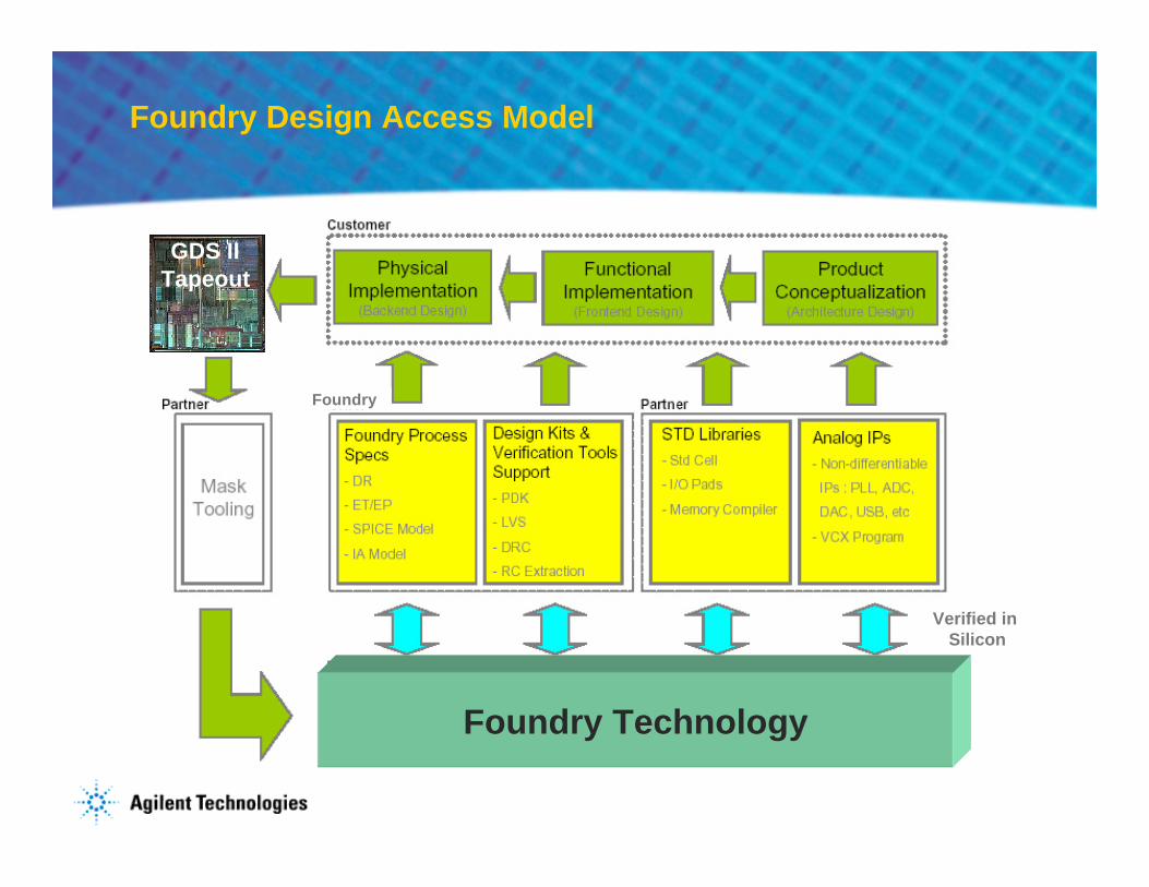
Foundry Design Access Model
Foundry Technology
Verified in Silicon
Foundry
GDS IITapeout
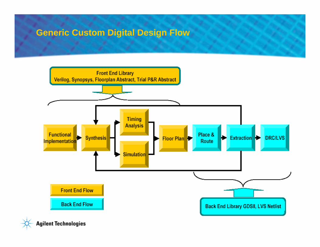
Generic Custom Digital Design Flow
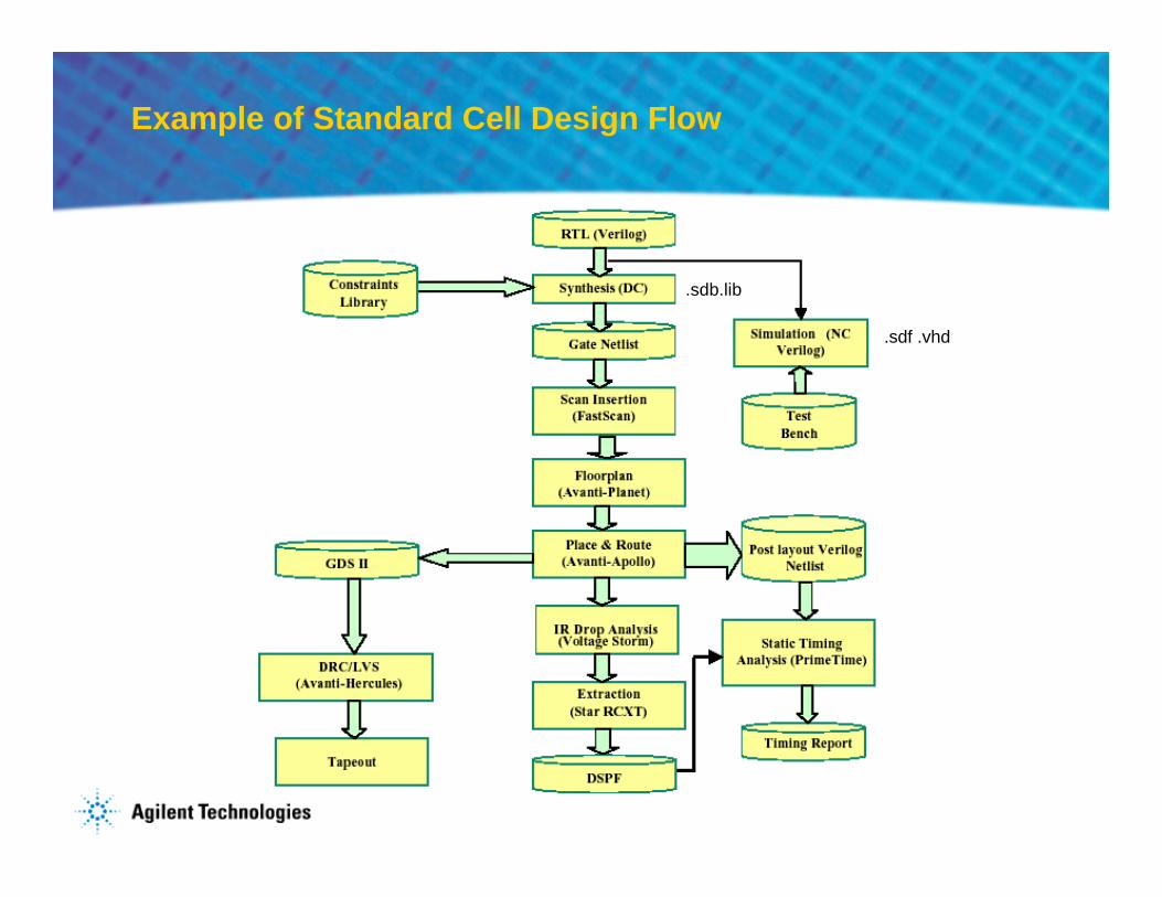
Example of Standard Cell Design Flow
.sdb.lib
.sdf .vhd

New Challenges in IC Design
Modern challenges in advanced semiconductor product designs can be divided into three broad areas:
1. Challenges in traditional design hierarchy (such as logic design, layout design) due to increased product functionality and SoC integration. => New EDA tools, technique, and methodology. (This is expected to lead to
further consolidation among EDA and design IP vendors).
2. Challenges related to shrinking technology: new materials, exponentially increasing leakages currents, increasingly complex interconnect structures, design related yield loss.=> The merger of design and manufacturing process development=> Further development of Design For Yield (DFY).
3. Challenges related to IP acquisition and management; mass production know-how.=> New emerging IP industry. => Technology research and manufacturing “constellations” (between major
foundries and IDMs)

Access to Complete Design Solutions
Various design solutions are available through foundries
DesignDesignToolsTools
LibraryLibrarySolutionSolution
DesignDesignServiceService
IPIPSolutionSolution
UNIVE
TurnkeyTurnkey
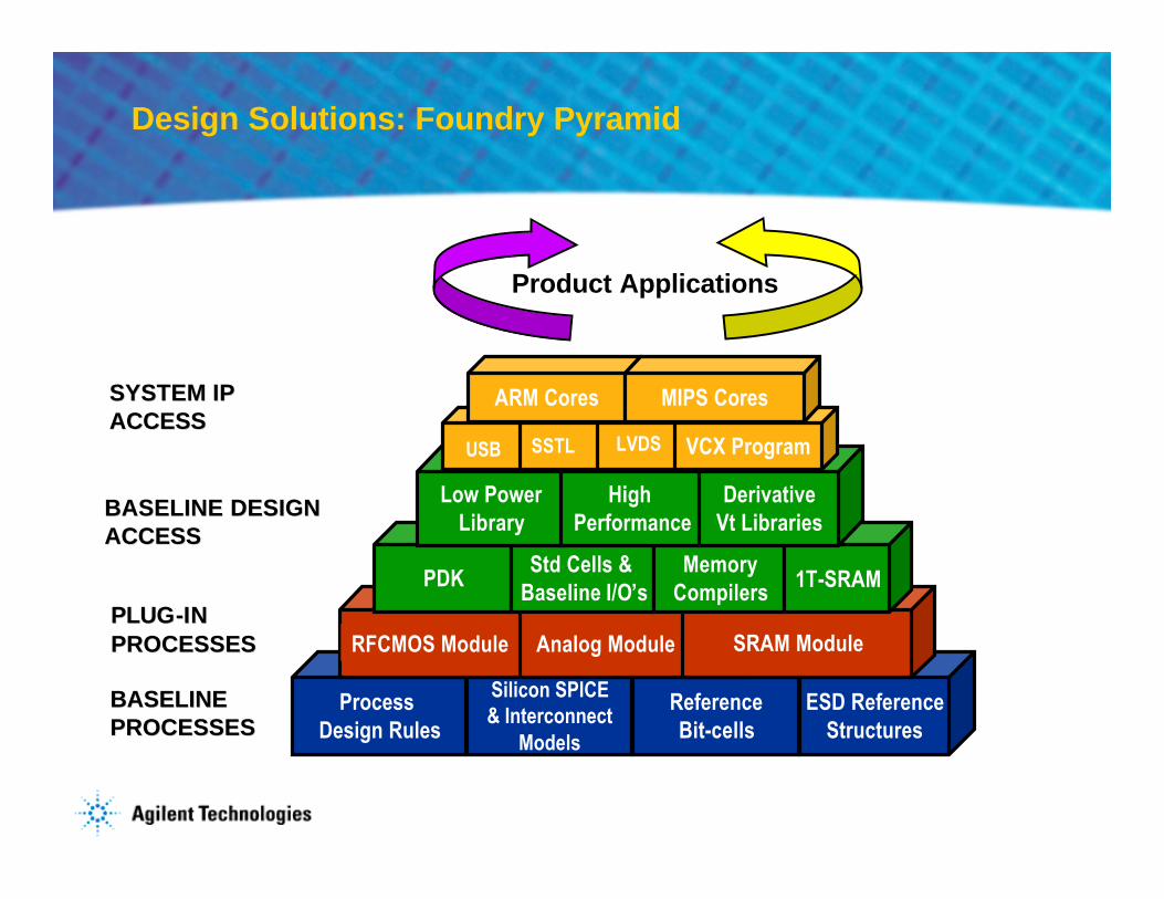
BASELINEBASELINEPROCESSESPROCESSES
PLUGPLUG--ININPROCESSESPROCESSES
BASELINE DESIGNBASELINE DESIGNACCESSACCESS
SYSTEM IPSYSTEM IPACCESSACCESS
Process Design Rules
Silicon SPICE& Interconnect
Models
ReferenceBit-cells
ESD ReferenceStructures
SRAM Module
PDKStd Cells &
Baseline I/O’sMemory
Compilers
Analog ModuleRFCMOS Module
Low PowerLibrary
High Performance
LVDS
ARM Cores
USB SSTL
1T-SRAM
DerivativeVt Libraries
VCX Program
MIPS Cores
Design Solutions: Foundry Pyramid
Product Applications

Design Access Considerations
Due to complexity of the problem and long term design
engagements, serious considerations have to be given to access
design solutions from a foundry.
Next we will examine some of the major aspects of design IP access
which needs to be analyzed and reviewed prior to foundry
engagement.
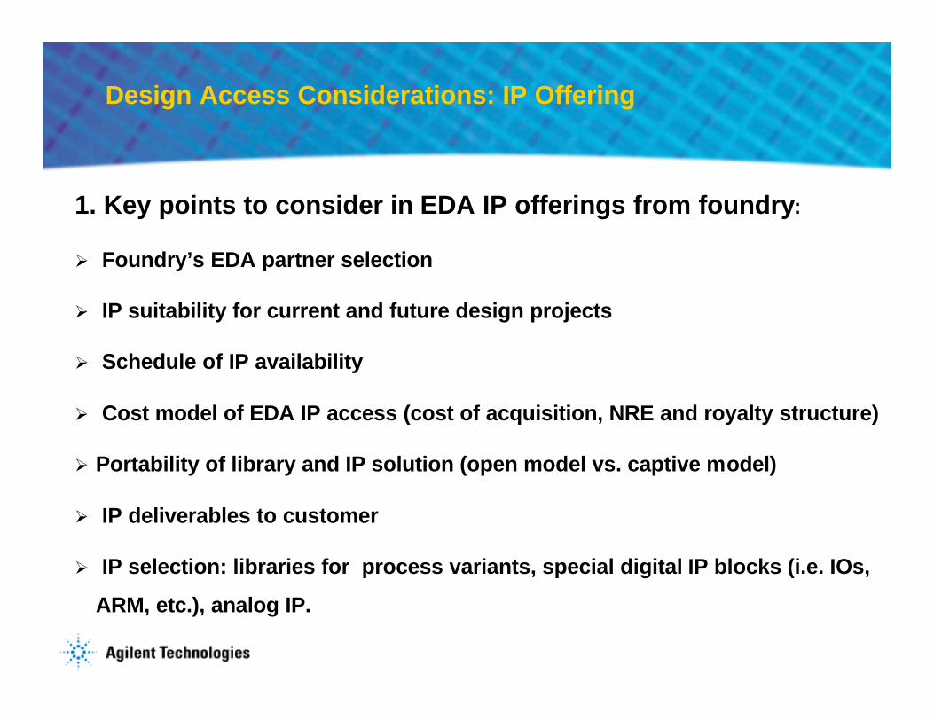
Design Access Considerations: IP Offering
1. Key points to consider in EDA IP offerings from foundry:
Ø Foundry’s EDA partner selection
Ø IP suitability for current and future design projects
Ø Schedule of IP availability
Ø Cost model of EDA IP access (cost of acquisition, NRE and royalty structure)
Ø Portability of library and IP solution (open model vs. captive model)
Ø IP deliverables to customer
Ø IP selection: libraries for process variants, special digital IP blocks (i.e. IOs,
ARM, etc.), analog IP.

Design Access Considerations: IP verification
2. EDA IP verification and characterization methodology:
Ø Foundry methodology to validate EDA libraries, compilers, etc.
- resources: expertise and tools
- silicon verified vs silicon hardened
Ø Process/SPICE changes:
- approval of changes in regards to EDA IP
- EDA IP characterization: time, schedule (before the changes or after)
- foundry’s flexibility for existing and on-going designs

Design Access Considerations: Design Support
3. Design support from foundry:
Ø Local expertise in different IP
Ø Foundry resources:
- engineers vs project managers
- design tools used at foundry
Ø Foundry support model
Ø Design services

Design Access Considerations: Final
4. IP Tapeout support:
Ø Procedures for “black box” models (i.e. ARM)
Ø IP tagging for royalty payments (i.e. specialized vs industry standard
VSIA)
Conclusion:
Selection of design IP from foundry makes a significant
difference in the long term success of foundry engagement. The
key elements discussed above need to be considered.
Libraries
Technology Files and PDK
Memory
IP Initiatives
Foundry Design Solutions
Foundry Design Solutions
Libraries
Technology Files and PDK
Memory
IP Initiatives

Foundry EDA Library Components
EDA library design solutions provided by major foundries usually consist of:
1. Standard Cell Libraries;
2. IO libraries;
3. Memory compilers and embedded special memories such as
embedded 1TSRAM, E2PROM, OTPROM, etc.
Each part of library solution has its unique challenges and requires special
considerations.
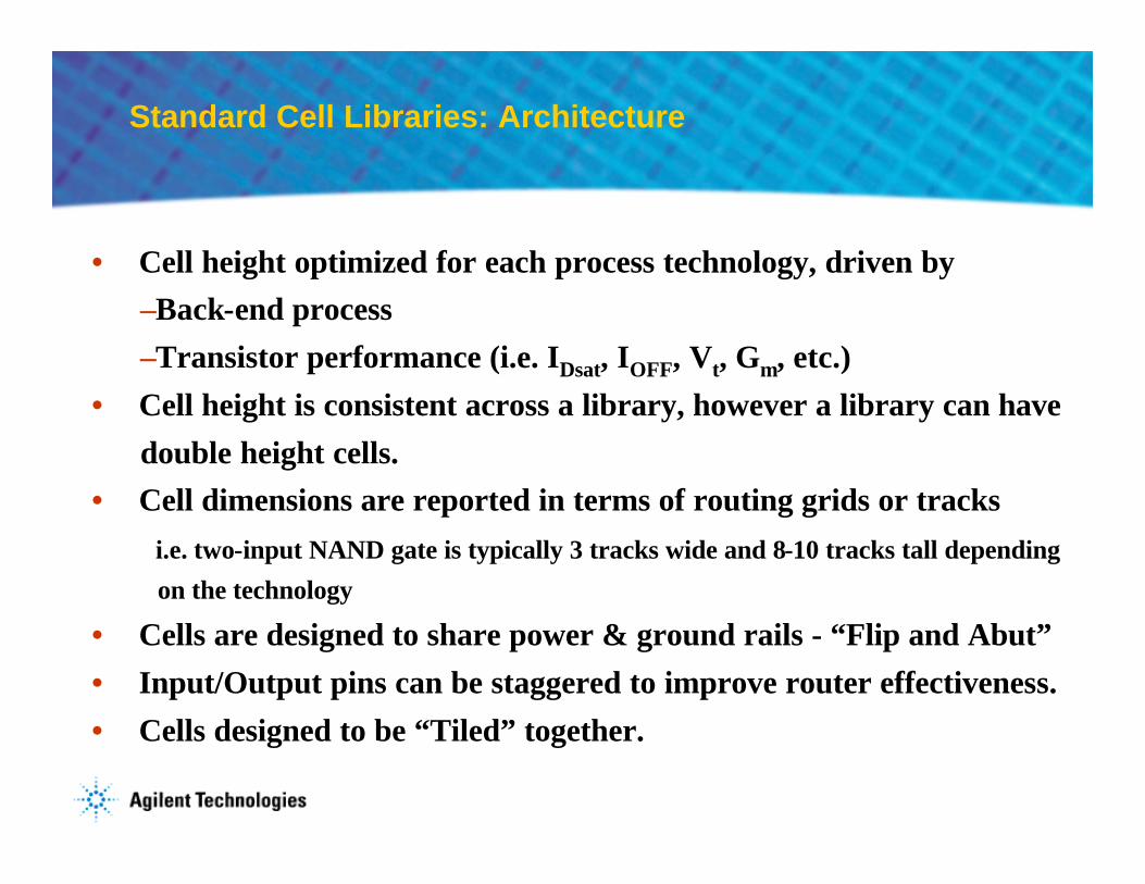
Standard Cell Libraries: Architecture
• Cell height optimized for each process technology, driven by–Back-end process–Transistor performance (i.e. IDsat, IOFF, Vt, Gm, etc.)
• Cell height is consistent across a library, however a library can have double height cells.
• Cell dimensions are reported in terms of routing grids or tracksi.e. two-input NAND gate is typically 3 tracks wide and 8-10 tracks tall depending
on the technology
• Cells are designed to share power & ground rails - “Flip and Abut”• Input/Output pins can be staggered to improve router effectiveness.• Cells designed to be “Tiled” together.

Typical Third Party Standard Cell Library Design Kit
Standard cell libraries from major IP providers typically include:• Front End Views
– Behavioral models– Simulation timing models:– Cadence NC-Verilog, NC-VHDL,Verilog-XL– Synopsys synthesis models– Design Compiler, Module Compiler, Physical Compiler,– Power Compiler– Synopsys PrimeTime Static Timing Models– Floorplan abstract
• Back End Views– Abstract Files for Place & Route Tools– CDL Netlists for LVS Verification– Physical (Layout) Files for Streaming Out GDSII Database
• Documentation: data-books, application notes

IO Library: Important Parameters
Key parameters of IO libraries:
• Pad Structure:– In-line pads for core limited designs: wide and short– Staggered pads for pad limited designs: narrow and tall
• IO cell height
• Pad pitch and pad opening– must be designed to meet particular assembly capabilities
• Separate I/O power rail– Accommodate I/O drive voltage requirement– Isolate “Noisy” I/O power from core power
• Simultaneous Switching Outputs - SSO– Guideline for the number of power pin pair requirements

Open Model Library Access: Chartered Semiconductor
Source: Chartered Semiconductor Manufacturing web site (http://www.charteredsemi.com/design/library_support.asp)

0.13µm Library Offerings
Source: Chartered Semiconductor Manufacturing web site (http://www.charteredsemi.com/design/library_support.asp)

Design Solutions
Libraries
Technology Files and PDK
Memory
IP Initiatives

l A PDK is a complete set of building blocks, generated from foundry’s technology files, that enables customers to create a custom IC design . PDK is most commonly implemented in Cadence design environment format. It must be aligned and verified with foundry’s process technology.
l PDK is the equivalent of a Standard Cell Library for digital design, providing an ‘off the shelf’, easy to install design environment tuned to a specific process technology.
Spice Models
DRC Runset
LVS Runset
Parasitic Extraction
PCells
What is a Foundry Process Design Kit (PDK)?
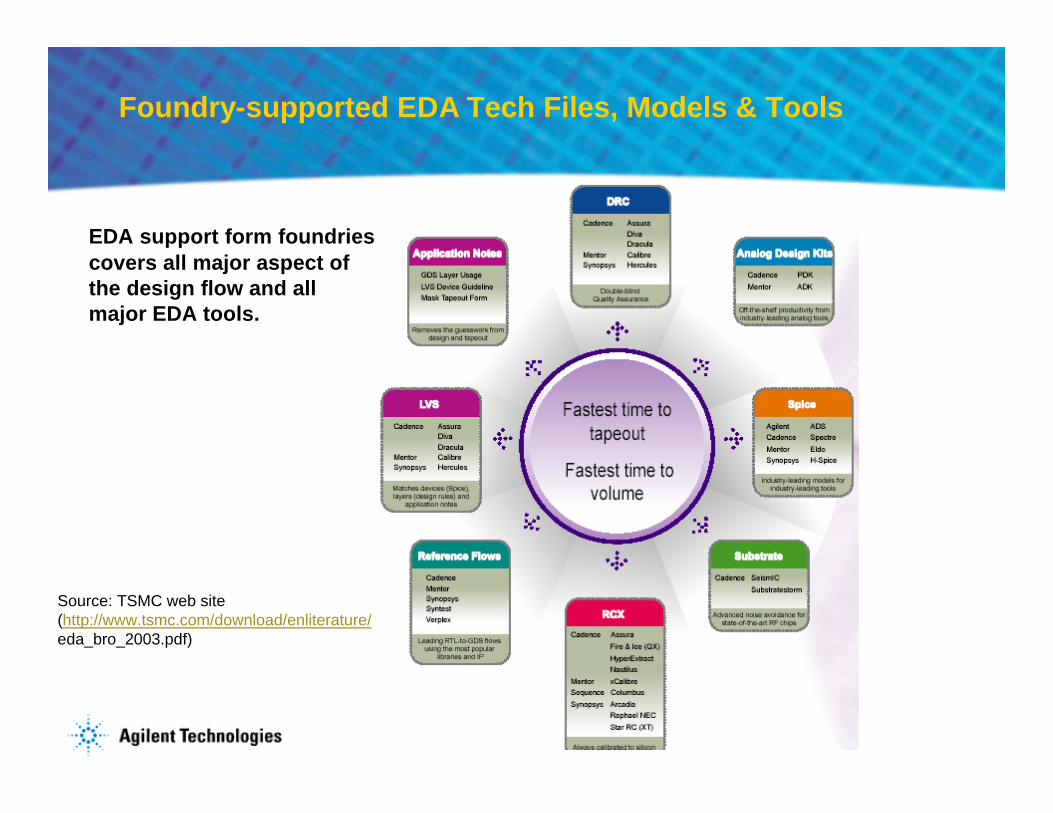
Foundry-supported EDA Tech Files, Models & Tools
EDA support form foundries covers all major aspect of the design flow and all major EDA tools.
Source: TSMC web site (http://www.tsmc.com/download/enliterature/eda_bro_2003.pdf)

Consistent with foundry technologies capabilities
Customers are able to design, simulate, layout, extract, verify & tape-out from transistor level upwards.
PDK Example: Cadence / Chartered PDK
Source: Chartered Semiconductor Manufacturing web site (http://www.charteredsemi.com/design/pdks.asp)

Foundry PDK
Panelists cite shortcomings of process design kitsBy Ron Wilson, EE Times, Mar 23, 2004 (http://www.eedesign.com/showArticle.jhtml?articleID=18401470)
Key points:
Foundry provided PDKs have to be used with caution and full understanding of theiradvantages, limitations and tradeoffs, as compared to in-house developed PDK.
• Change of process may not be reflected in PDK.
• With the growing complexity and rate of change in processes, IP vendors will be unable to keep their IP current with the process... "It's very likely that the IP you use will have been developed with a different PDK from the one you are using. That will be trouble.“ - Dan Hillman, VP Virtual Silicon
• PDK revision control.

Design Solutions
Libraries
Technology Files and PDK
Memory
IP Initiatives
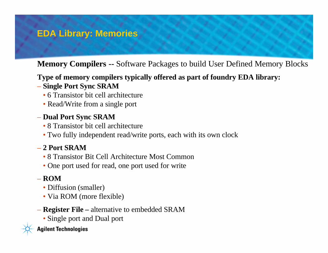
EDA Library: Memories
Memory Compilers -- Software Packages to build User Defined Memory Blocks
Type of memory compilers typically offered as part of foundry EDA library:– Single Port Sync SRAM
• 6 Transistor bit cell architecture• Read/Write from a single port
– Dual Port Sync SRAM• 8 Transistor bit cell architecture• Two fully independent read/write ports, each with its own clock
– 2 Port SRAM• 8 Transistor Bit Cell Architecture Most Common• One port used for read, one port used for write
– ROM• Diffusion (smaller)• Via ROM (more flexible)
– Register File – alternative to embedded SRAM• Single port and Dual port

Compiled SRAM: Example
Typical Compiled embedded SRAM Architecture
A lot of memory “overhead” is part of generated SRAM. Compiled register file may be a good alternative to small SRAM.

Design Solutions
Libraries
Technology Files and PDK
Memory
IP Initiatives

Foundry
UNIVE
and many many others …
Available Foundry IP Initiatives

Foundry supported IP alliances program allows:
l Compare and select from various third-party IP solutions
l Silicon hardened and proven at various foundries
l IP is listed against industry standard specifications, e.g. VSIA (Virtual Socket Integration Assoc. )
l IP provider states level of validation and specific silicon processes in which it has been hardened
l Customers have access to more silicon hardened IP, reducing risk and exposure
l IP flexibility and ownership are understood prior to engagement
Benefits for Customers

New Economical Realities for Custom IC

New World of Custom IC Product Design
Cost of new ASIC designs increase with every technology generation:
Average design cost: EDA/COT tools, design engineering, mask set, prototyping, test.
Design cost for technology
0.85
0.73
1
2
3
4
5
6
7
8
9
10
0.090.10.110.120.130.140.150.160.170.18
Technology, um
Des
ign
co
st, $
M
0.6
0.7
0.8
0.9
1.0
Rel
ativ
e d
ie a
rea
Total design cost ($M)Relative die area

New World of Custom IC Product Design
The business dynamics of custom IC products changed:
ASIC ≠ LOW COST
Market response:
- High volume ASIC applications (i.e. consumer electronics)
- High performance ASIC applications (at premium cost)
- ASSP
- New technologies such as FPGA core with standard cell ASIC:
for example, from IBM/Xilinx, reconfigurable ASIC core from LSI, etc.

ASIC vs ASSP
Custom IC Device market forecast (in $B)(all categories)
31.2
49.1
29.926.8
19.822.5
28.1
32.5
40.1
46.3
10
20
30
40
50
2002 2003 2004 2005 2006year
TAM
, $B
ASICASSP
Source: Gartner Research Semiconductor Forecast, 2003
The gap between ASIC and ASSP is projected to widen
43% TAM growth over 4 years
35% TAM growth over 4 years
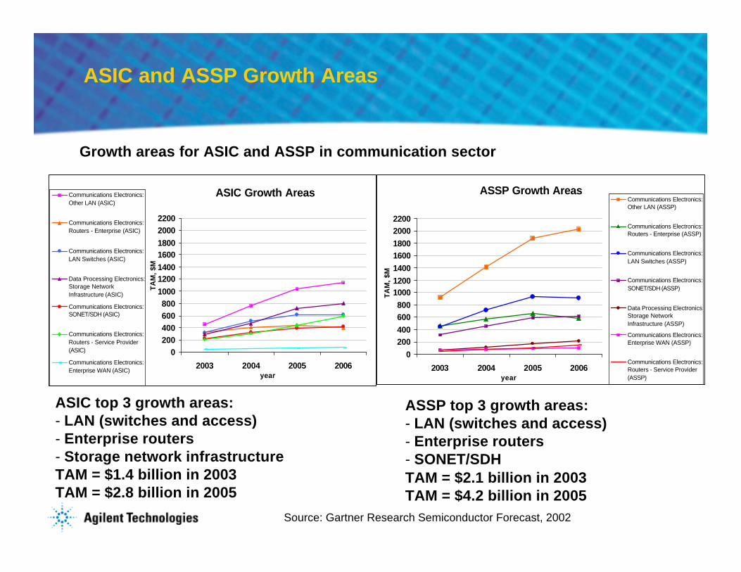
ASIC and ASSP Growth Areas
ASIC Growth Areas
0200400600800
1000120014001600180020002200
2003 2004 2005 2006year
TAM
, $M
Communications Electronics:Other LAN (ASIC)
Communications Electronics:Routers - Enterprise (ASIC)
Communications Electronics:LAN Switches (ASIC)
Data Processing Electronics:Storage NetworkInfrastructure (ASIC)
Communications Electronics:SONET/SDH (ASIC)
Communications Electronics:Routers - Service Provider(ASIC)
Communications Electronics:Enterprise WAN (ASIC)
ASSP Growth Areas
0200400600800
1000120014001600180020002200
2003 2004 2005 2006year
TA
M, $
M
Communications Electronics:Other LAN (ASSP)
Communications Electronics:Routers - Enterprise (ASSP)
Communications Electronics:LAN Switches (ASSP)
Communications Electronics:SONET/SDH (ASSP)
Data Processing Electronics:Storage NetworkInfrastructure (ASSP)
Communications Electronics:Enterprise WAN (ASSP)
Communications Electronics:Routers - Service Provider(ASSP)
Source: Gartner Research Semiconductor Forecast, 2002
ASIC top 3 growth areas:- LAN (switches and access)- Enterprise routers- Storage network infrastructureTAM = $1.4 billion in 2003TAM = $2.8 billion in 2005
ASSP top 3 growth areas:- LAN (switches and access)- Enterprise routers- SONET/SDHTAM = $2.1 billion in 2003TAM = $4.2 billion in 2005
Growth areas for ASIC and ASSP in communication sector
Summary
• Foundries offer complete design access in addition to process, tech files, and libraries
• Foundries are becoming active participants in design process.
• Foundries EDA IP engagements need to be carefully evaluated against current and future design needs
• Design IP access model needs to be taken into considerations for a long term foundry engagement.
• Cost of custom designs is increasing rapidly for more advanced technologies.First time TO success is crucial for success => extensive and accurate simulation, virtual prototyping, design for yield.