
design of waveguide bandpass filter in the x-frequency band
16
1 DESIGN OF WAVEGUIDE BANDPASS FILTER IN THE X-FREQUENCY BAND Gaëtan Prigent, Nathalie Raveu, Olivier Pigaglio, Henri Baudrand How to design a broad bandpass filter in the X-frequency range? The design procedure is developed from synthesis to electromagnetic simulation. The filter to be designed is implemented in waveguide technology with inductive irises coupling sections. So as to evaluate equivalent susceptance of iris aperture, two methods were used: the first one is based on classical mode matching techniques, whereas the second uses electromagnetic-based equivalent circuit. The susceptance values ensued from these methods were then compared. Validations for both methods were carried out using Ansoft-HFSS electromagnetic simulations and measurements. I. INTRODUCTION The design of passive microwave functions, and especially filters, is a study domain of the most important interest. Indeed, with the widespread applications of communication systems, the bandpass filter is an essential component. Thus, the quality of filter is extremely important. The development of bandpass filters has emphasized high electrical performances in terms of insertion losses and selectivity. Within this context, designers are faced to several problems linked to the design control, in keeping with the modeling accuracy. The design of such filters requires specific techniques which cover a wide spectrum of knowledge. Students must be introduced to that necessary knowledge that will make them immediately productive upon graduation. The present paper deals with filter design techniques taught to students in second year of engineering school. During their courses, students get acquainted with filter synthesis techniques, microwave transmission lines analyses, electromagnetic model techniques as well as simulation software, either circuit (Agilent-ADS) or electromagnetic (Ansoft-HFSS) frameworks. The present study recount practical works that gather this entire knowledge and allow students their application in concrete case. Development of filter design rests on three steps. Application of Tchebycheff theory is first performed. So as to meet the filter specifications, the filter order is determined as well as its lumped element circuit prototype. In expectation of the filter implementation into waveguide technology, that limits the achievable impedance range, synthesis techniques based on impedance inverters and series resonators are then introduced. Implementation into waveguide technology requires equivalent network for impedance inverters. From circuit analyze point of view, impedance inverter are modeled as inductance set in parallel. Implementation of the whole cascaded elements of the filter is then performed on Matlab. The circuit analyze results evidenced the difference between lumped- (Tchebycheff theory) and semi-lumped- (Richards transformation) elements representation. Hence, so as to meet the expected specifications, further analyses were carried out to define the appropriate filter order.
Transcript of design of waveguide bandpass filter in the x-frequency band
1
DESIGN OF WAVEGUIDE BANDPASS FILTER IN THE X-FREQUENCY BAND
Gaëtan Prigent, Nathalie Raveu, Olivier Pigaglio, Henri Baudrand
How to design a broad bandpass filter in the X-frequency range? The design procedure is developed from synthesis to
electromagnetic simulation. The filter to be designed is implemented in waveguide technology with inductive irises coupling sections.
So as to evaluate equivalent susceptance of iris aperture, two methods were used: the first one is based on classical mode matching
techniques, whereas the second uses electromagnetic-based equivalent circuit. The susceptance values ensued from these methods were
then compared. Validations for both methods were carried out using Ansoft-HFSS electromagnetic simulations and measurements.
I. INTRODUCTION
The design of passive microwave functions, and especially filters, is a study domain of the most important interest. Indeed, with
the widespread applications of communication systems, the bandpass filter is an essential component. Thus, the quality of filter
is extremely important. The development of bandpass filters has emphasized high electrical performances in terms of insertion
losses and selectivity. Within this context, designers are faced to several problems linked to the design control, in keeping with
the modeling accuracy. The design of such filters requires specific techniques which cover a wide spectrum of knowledge.
Students must be introduced to that necessary knowledge that will make them immediately productive upon graduation.
The present paper deals with filter design techniques taught to students in second year of engineering school. During their
courses, students get acquainted with filter synthesis techniques, microwave transmission lines analyses, electromagnetic model
techniques as well as simulation software, either circuit (Agilent-ADS) or electromagnetic (Ansoft-HFSS) frameworks. The
present study recount practical works that gather this entire knowledge and allow students their application in concrete case.
Development of filter design rests on three steps. Application of Tchebycheff theory is first performed. So as to meet the filter
specifications, the filter order is determined as well as its lumped element circuit prototype. In expectation of the filter
implementation into waveguide technology, that limits the achievable impedance range, synthesis techniques based on
impedance inverters and series resonators are then introduced.
Implementation into waveguide technology requires equivalent network for impedance inverters. From circuit analyze point
of view, impedance inverter are modeled as inductance set in parallel. Implementation of the whole cascaded elements of the
filter is then performed on Matlab. The circuit analyze results evidenced the difference between lumped- (Tchebycheff theory)
and semi-lumped- (Richards transformation) elements representation. Hence, so as to meet the expected specifications, further
analyses were carried out to define the appropriate filter order.
2
In a second time, inductances are realized by vertical iris apertures which dimensions are calculated using two methods. The
first one is a conventional mode matching technique [1] whereas the second uses analytical approximation based on
electromagnetic equivalent circuit [2]-[3], which concepts are detailed in part IV. Validation of both methods is achieved
through electromagnetic simulations using Ansoft-HFSS electromagnetic simulator as well as experimental results presented.
This approach shows the strong link between lumped circuit and the electromagnetic modelisation which leads suited physical
dimensions for the device.
II. BASE-FILTER DESIGN PROCEDURE
A. Lumped Elements Design
The filter to be designed is a Tchebycheff bandpass filter in the X frequency range. Hence, the waveguide used is a WR90
with 0.9 inch x 0.4 inch section. The central frequency of the filter was determined with respect to single mode propagation.
Hence, according to the waveguide dimensions, the first propagating mode is a TE10 mode with 6.56-GHz cutoff frequency,
whereas the first higher-order mode is a TE20 with 13.12-GHz cutoff frequency. Hence a central frequency (f0) of 9.84-GHz was
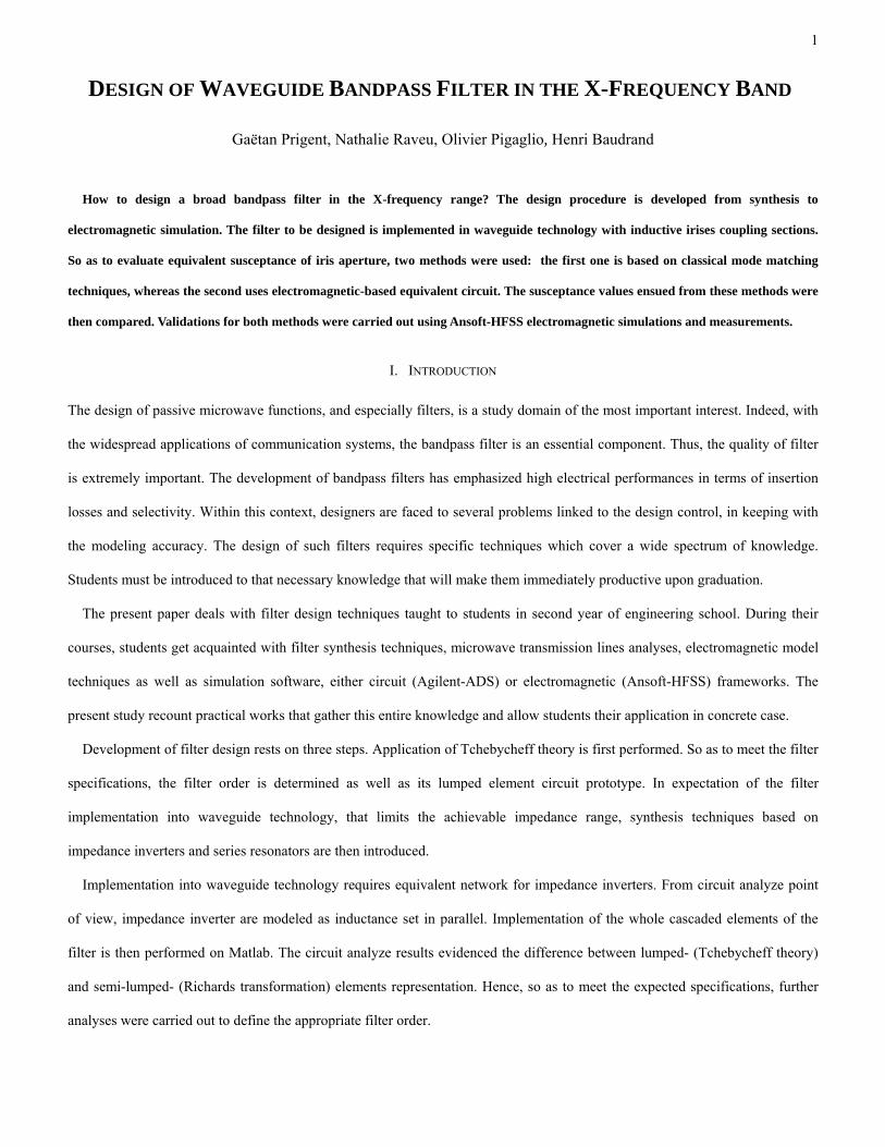
chosen which corresponds to the center frequency of the mono-mode band. Finally, the 40-dB rejection level (Lar) is calculated
as in (1) [4]-[5]:
f (GHz)S21(dB)
Lar=-40
Las=-0.1f0=9.84 fr=?
δ=0.2*f0
Fig. 1. Bandpass filter specifications.
021*2.1 ff r ⎟
⎠⎞
⎜⎝⎛ +=
δ
(1)
where δ is the filter relative bandwidth (δ=0.2). The filter specifications are depicted in Fig. 1.
The first conception step consists in the determination of the order of the equivalent low-pass filter prototype, which is the
base-network for filter synthesis, whatever the filter type is, high-pass, band-pass or stop-band. It is well known that lowpass
prototype filter can be transformed into bandpass response using the frequency substitution (2):
3
⎟⎟⎠
⎞⎜⎜⎝
⎛−←
ωω
ωω
δω 0
0
*1' (2)
where δ is the fractional bandwidth of the passband, and ω0 the center frequency. Application of this transformation with ω=ωr,
allows to evaluate the reject frequency (ω'r) of the lowpass prototype. Then, the filter order is determined using the equation (2):
)'(110
110 1
10
101
rLar
Las
chchN ω−−
−
−≥
(3)
For the specified criterion a 5th-order filter is necessary. The base lowpass prototype network is depicted in Fig. 2, where
normalized inductance and capacitance values assumed to be the Tchebycheff coefficients (gi) determined with (4) to (7).
R0=g0 R6=g6C1=g1
L2=g2
C3=g3
L4=g4
C5=g5
Fig. 2. 5th-order lowpass prototype filter.
⎥⎥⎦
⎤
⎢⎢⎣
⎡⎟⎟⎠
⎞⎜⎜⎝
⎛=
37.17cothln
Lasβ ⎟
⎠⎞
⎜⎝⎛=
N2sinh βγ (4)
⎟⎠⎞
⎜⎝⎛ −
== Nia Nii 2
)12(sin..1π ⎟
⎠⎞
⎜⎝⎛+== N
ib Niiπγ 22
..1 sin (5)
10 =g γ
11
2ag =
11
1..2
4
−−
−= =
ii
iiNii gb
aag (6)
⎪⎩
⎪⎨
⎧
⎟⎠⎞
⎜⎝⎛=
=
+
+
evenNforg
oddNforg
N
N
4coth
1
21
1
β (7)
L'iL"i=
C"i=
C'i
L'iδω0
δω0L'i
Lowpass Element Bandpass Elements
L"i=δ
ω0C'iC"i=
C'iδω0
Fig. 3. Lowpass to bandpass transformation.
4
This lowpass network is normalized with respect to a 1-Ω load and source resistances and has a 1 rad/s cut-off frequency.
Hence, to obtain the desired frequency and impedance level, one needs to employ the proper transformations to scale the
component values of the prototype networks (4)-(9). Indeed, a source impedance Z0 (Z0=ZTE10) can be obtained by multiplying
the impedance of the filter by Z0.
Moreover, the change of cutoff frequency from unity to ω0 requires that we scale the frequency dependence of the filter by the
factor 1/ω0. As a consequence, considering a normalized values zL and zC, impedance and frequency scaling result in:
ωω
ωω '0
0 jLLZjZjLz LL ==→= (8)
ωω
ωω '0
0 jCCYjYjCy cC ==→= (9)
which shows that the new element values are given by
0
0'ω
LZL = and 00
'ωZ
CC = (10)
The bandpass filter elements can be obtained using the frequency substitution (2) for the series reactance and shunt
susceptance of lowpass prototype.
ωω
δωω
δωωω ''
'''
0
0
''
.1
.'
ii
iiii Cj
jLj
LLjjLjX +=+→= (11)
ωω
δωω
δωωω ''
'''
0
0
''
.1
.'
ii
iiii Lj
jCj
CCjjCjB +=+→= (12)
Thus, a series inductor Li’ is transformed to a series Li” -Ci” circuit and a shunt capacitor Ci’ is transformed into shunt Li”-Ci”
circuit using rules described in Fig. 3. As a result, the desired bandpass filter prototype is depicted in Fig. 4.
To do so, each series reactance Xs and shunt susceptances Bp were replaced with their ABCD matrix, respectively
⎟⎟⎠
⎞⎜⎜⎝
⎛=
101 jXs
T and (13) ⎟⎟⎠
⎞⎜⎜⎝
⎛=
101
jBpT
ZTE10 ZTE10L"1C"1
L"2C"2
C"3
C"4
C"5L"3
L"4
L"5
Fig. 4. 5th-order bandpass prototype filter.
5
TABLE I
VALUES OF THE BANDPASS FILTER LUMPED ELEMENTS
RESONATORS
1 & 5
RESONATORS
2 & 4
RESONATOR
3
L’’ (nH) 0.996 36.16 0.5794
C’’ (pF) 0.2626 6.68.10-3 0.4522
7 8 9 10 11 12 13-50
-45
-40
-35
-30
-25
-20
-15
-10
-5
0
Frequency (GHz)
dB(S
11),
dB(S
12)
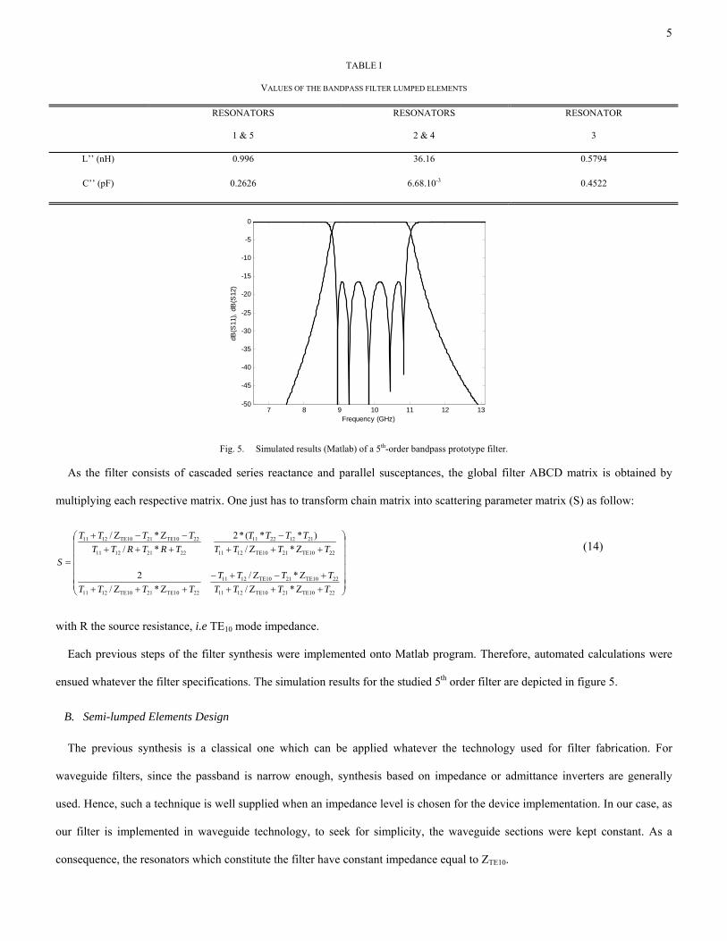
Fig. 5. Simulated results (Matlab) of a 5th-order bandpass prototype filter.
As the filter consists of cascaded series reactance and parallel susceptances, the global filter ABCD matrix is obtained by
multiplying each respective matrix. One just has to transform chain matrix into scattering parameter matrix (S) as follow:
⎟⎟⎟⎟⎟⎟
⎠
⎞
⎜⎜⎜⎜⎜⎜
⎝
⎛
++++−+−
+++
+++−
+++−−+
=
22TE1021TE101211
22TE1021TE101211
22TE1021TE101211
22TE1021TE101211
21122211
22211211
22TE1021TE101211
Z*Z/Z*Z/
Z*Z/2
Z*Z/)**(*2
*/Z*Z/
TTTTTTTT
TTTT
TTTTTTTT
TRTRTTTTTT
S (14)
with R the source resistance, i.e TE10 mode impedance.
Each previous steps of the filter synthesis were implemented onto Matlab program. Therefore, automated calculations were
ensued whatever the filter specifications. The simulation results for the studied 5th order filter are depicted in figure 5.
B. Semi-lumped Elements Design
The previous synthesis is a classical one which can be applied whatever the technology used for filter fabrication. For
waveguide filters, since the passband is narrow enough, synthesis based on impedance or admittance inverters are generally
used. Hence, such a technique is well supplied when an impedance level is chosen for the device implementation. In our case, as
our filter is implemented in waveguide technology, to seek for simplicity, the waveguide sections were kept constant. As a
consequence, the resonators which constitute the filter have constant impedance equal to ZTE10.
6
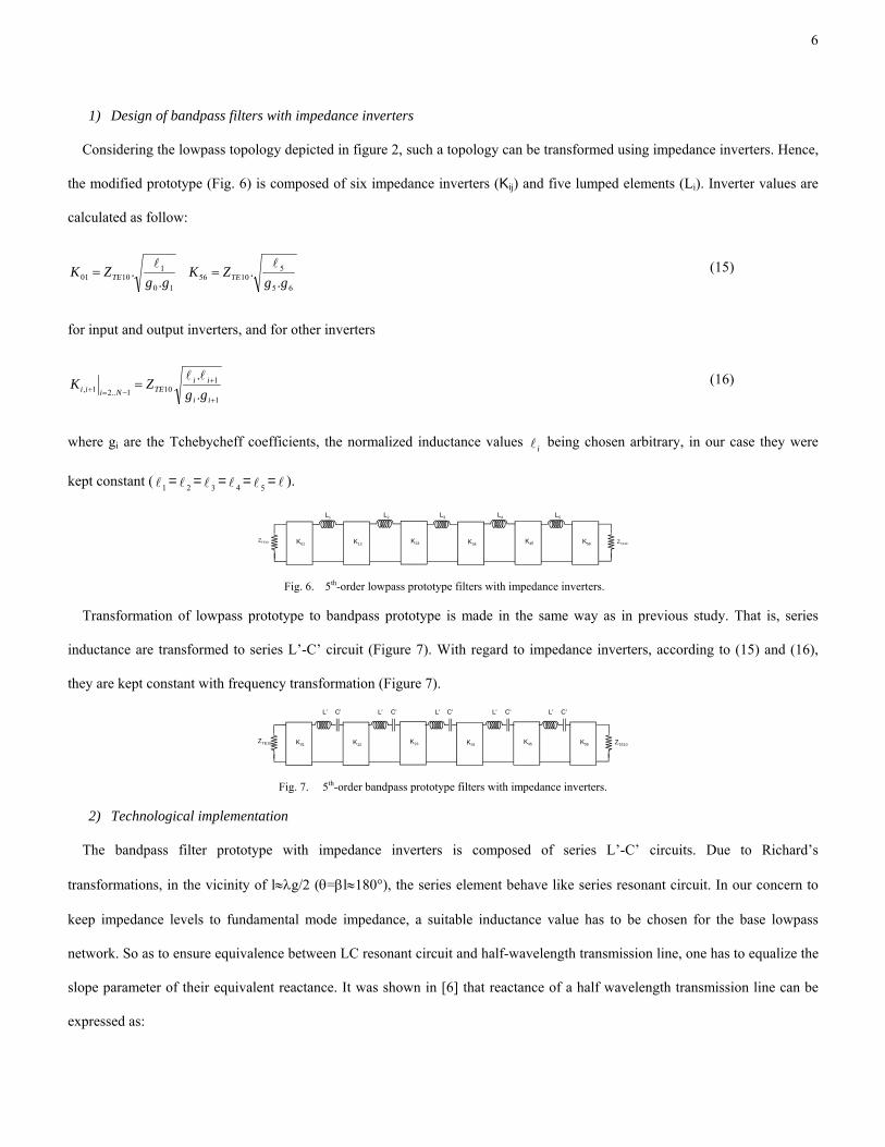
1) Design of bandpass filters with impedance inverters
Considering the lowpass topology depicted in figure 2, such a topology can be transformed using impedance inverters. Hence,
the modified prototype (Fig. 6) is composed of six impedance inverters (Kij) and five lumped elements (Li). Inverter values are
calculated as follow:
10
11001 .
.gg
ZK TEl
= 65
51056 .
.gg
ZK TEl
= (15)
for input and output inverters, and for other inverters
1
1101..21, .
.
+
+−=+ =
ii
iiTENiii gg
ZK ll (16)
where gi are the Tchebycheff coefficients, the normalized inductance values being chosen arbitrary, in our case they were
kept constant ( = = = = = l ).
il
1l 2l 3l 4l 5l
ZTE10
L1
K01 K12 K23 K34 K45 K56 ZTE10
L2 L3 L4 L5
Fig. 6. 5th-order lowpass prototype filters with impedance inverters.
Transformation of lowpass prototype to bandpass prototype is made in the same way as in previous study. That is, series
inductance are transformed to series L’-C’ circuit (Figure 7). With regard to impedance inverters, according to (15) and (16),
they are kept constant with frequency transformation (Figure 7).
ZTE10
L'
K01 K12 K23 K34 K45 K56 ZTE10
L' L' L' L'C' C' C' C' C'
Fig. 7. 5th-order bandpass prototype filters with impedance inverters.
2) Technological implementation
The bandpass filter prototype with impedance inverters is composed of series L’-C’ circuits. Due to Richard’s
transformations, in the vicinity of l≈λg/2 (θ=βl≈180°), the series element behave like series resonant circuit. In our concern to
keep impedance levels to fundamental mode impedance, a suitable inductance value has to be chosen for the base lowpass
network. So as to ensure equivalence between LC resonant circuit and half-wavelength transmission line, one has to equalize the
slope parameter of their equivalent reactance. It was shown in [6] that reactance of a half wavelength transmission line can be
expressed as:
7
⎟⎟⎠
⎞⎜⎜⎝
⎛−=
ωω
ωωπ 0
00 .
2.ZX (17)
Thus, its slope parameter is
22 00
πω
ω
ωω
ZXS =∂∂
==
(18)
Moreover, the reactance of L’C’ equivalent circuit is
'1'C
LX eq ωω −= (19)
which, considering resonant condition (L’C’ω2=1), results in a slope parameter of: .
0'2
0
ωω
ω
ωω
LX
S eqeq =
∂
∂=
=
(20)
Hence, equivalence is obtained for inductance value for the passband prototype of:
0
0
2'
ωπ ZL = (21)
which means that, the normalized inductance value that has to be taken into account in the base lowpass prototype inverter
calculation is (22), with regards to transformations depicted in figure 3:
2δπ
=l (22)
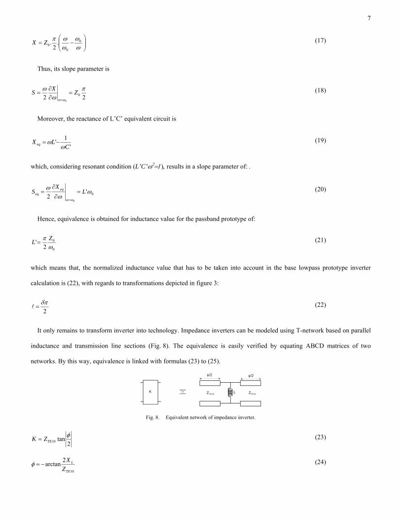
It only remains to transform inverter into technology. Impedance inverters can be modeled using T-network based on parallel
inductance and transmission line sections (Fig. 8). The equivalence is easily verified by equating ABCD matrices of two
networks. By this way, equivalence is linked with formulas (23) to (25).
ZTE10 ZTE10
φ/2 φ/2
LK
Fig. 8. Equivalent network of impedance inverter.
2tan10
φTEZK = (23)
10
2arctanTE
L
ZX
−=φ (24)
8
2
10
10
10 1 ⎟⎠⎞⎜
⎝⎛−
=
TE
TE
TEZ
K
ZK
ZX (25)
As a consequence, inverters can be realized using inductive irises and additional transmission lines. The final bandpass filter
can be synthesized as depicted in Fig. 9, with effective resonators lengths given by (26):
⎟⎟⎠
⎞⎜⎜⎝
⎛ ++= +−
= πφφλ
21
21,,1
..1
iiiig
NiresiL (26)
ZTE10
Lres1
L01ZTE10 ZTE10ZTE10
Lres2
L12 ZTE10
Lres3
L23 ZTE10
Lres4
L34 ZTE10
Lres5
L45 L56
Fig. 9. 5th order Bandpass filter network.
d1
d2
d3
Lres1
Lres2
Lres3
Lres4
Lres5d4
d5
d6
Fig. 10. 5th order Bandpass semi-lumped elements filter simulation results (Matlab).
TABLE 2
VALUES OF THE 5TH BANDPASS FILTER SEMI-LUMPED ELEMENTS
WAVEGUIDE LENGTH
(mm) SUSCEPTANCE
INDUCTANCE
(nH)
Lres1=Lres5=15.7 b1=b6=1.3872 L1=L6=4.17
Lres2=Lres4=17.6 b2=b5=3.7411 L2=L5=1.527
Lres3=18 b3=b4=5.0474 L3=L4=1.132
III. MATLAB SIMULATION RESULTS
The global filter was simulated onto Matlab with nominal dimensions given in Table 2. One should note that the filter
bandwidth was significantly reduced (Fig. 10). This is due to the equivalent model used for impedance inverters. Hence, such a
model is usually used since the bandwidth is narrow enough. In the studied case, as the relative bandwidth to be reached is 20%,
9
the model is out of the model validity domain, approximation based on the slope parameter being available in the vicinity of the
central frequency.
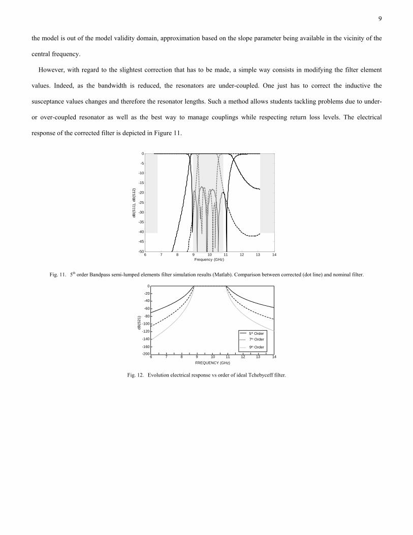
However, with regard to the slightest correction that has to be made, a simple way consists in modifying the filter element
values. Indeed, as the bandwidth is reduced, the resonators are under-coupled. One just has to correct the inductive the
susceptance values changes and therefore the resonator lengths. Such a method allows students tackling problems due to under-
or over-coupled resonator as well as the best way to manage couplings while respecting return loss levels. The electrical
response of the corrected filter is depicted in Figure 11.
6 7 8 9 10 11 12 13 14-50
-45
-40
-35
-30
-25
-20
-15
-10
-5
0
Frequency (GHz)
dB(S
11),
dB(S
12)
Fig. 11. 5th order Bandpass semi-lumped elements filter simulation results (Matlab). Comparison between corrected (dot line) and nominal filter.
dB
(S21
)
0
-100
-120
-140
-160
-2007 8 9 10 11 12 13
FREQUENCY (GHz)6 14
5th Order7th Order
9th Order
-80
-60
-40
-20
Fig. 12. Evolution electrical response vs order of ideal Tchebyceff filter.
10
6 7 8 9 10 11 12 13 14-50
-45
-40
-35
-30
-25
-20
-15
-10
-5
0
Frequency (GHz)
dB(S
11),
dB(S
12)
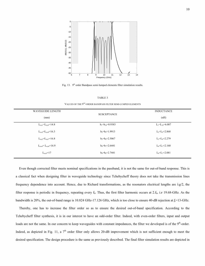
Fig. 13. 9th order Bandpass semi-lumped elements filter simulation results.
TABLE 3
VALUES OF THE 9TH-ORDER BANDPASS FILTER SEMI-LUMPED ELEMENTS
WAVEGUIDE LENGTH
(mm) SUSCEPTANCE
INDUCTANCE
(nH)
Lres1=Lres9=14.8 b1=b10=0.9383 L1=L10=6.087
Lres2=Lres8=16.3 b2=b9=1.9913 L2=L9=2.868
Lres3=Lres7=16.8 b3=b8=2.5067 L3=L8=2.279
Lres4= Lres6=16.9 b4=b7=2.6441 L4=L7=2.160
Lres5=17 b4=b6=2.7441 L4=L7=2.081
Even though corrected filter meets nominal specifications in the passband, it is not the same for out-of-band response. This is
a classical fact when designing filter in waveguide technology since Tchebycheff theory does not take the transmission lines
frequency dependence into account. Hence, due to Richard transformations, as the resonators electrical lengths are λg/2, the
filter response is periodic in frequency, repeating every f0. Thus, the first filter harmonic occurs at 2.f0, i.e 19.68-GHz. As the
bandwidth is 20%, the out-of-band range is 10.824 GHz-17.126 GHz, which is too close to ensure 40-dB rejection at fr=13-GHz.
Thereby, one has to increase the filter order so as to ensure the desired out-of-band specification. According to the
Tchebycheff filter synthesis, it is in our interest to have an odd-order filter. Indeed, with even-order filters, input and output
loads are not the same. In our concern to keep waveguides with constant impedances, the filter we developed is of the 9th-order.
Indeed, as depicted in Fig. 11, a 7th order filter only allows 20-dB improvement which is not sufficient enough to meet the
desired specification. The design procedure is the same as previously described. The final filter simulation results are depicted in
11
Fig. 12, with its elements values given in Table 3.
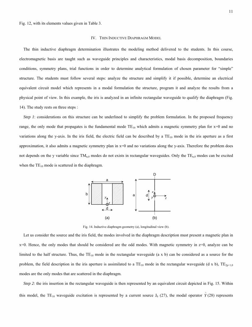
IV. THIN INDUCTIVE DIAPHRAGM MODEL
The thin inductive diaphragm determination illustrates the modeling method delivered to the students. In this course,
electromagnetic basis are taught such as waveguide principles and characteristics, modal basis decomposition, boundaries
conditions, symmetry plans, trial functions in order to determine analytical formulation of chosen parameter for “simple”
structure. The students must follow several steps: analyze the structure and simplify it if possible, determine an electrical
equivalent circuit model which represents in a modal formulation the structure, program it and analyze the results from a
physical point of view. In this example, the iris is analyzed in an infinite rectangular waveguide to qualify the diaphragm (Fig.
14). The study rests on three steps :
Step 1: considerations on this structure can be underlined to simplify the problem formulation. In the proposed frequency
range, the only mode that propagates is the fundamental mode TE10 which admits a magnetic symmetry plan for x=0 and no
variations along the y-axis. In the iris field, the electric field can be described by a TE10 mode in the iris aperture as a first
approximation, it also admits a magnetic symmetry plan in x=0 and no variations along the y-axis. Therefore the problem does
not depends on the y variable since TMn,0 modes do not exists in rectangular waveguides. Only the TEn,0 modes can be excited
when the TE10 mode is scattered in the diaphragm.
a
by
z
d
y z
xda
D
(a) (b)
Fig. 14. Inductive diaphragm geometry (a), longitudinal view (b).
Let us consider the source and the iris field, the modes involved in the diaphragm description must present a magnetic plan in
x=0. Hence, the only modes that should be considered are the odd modes. With magnetic symmetry in z=0, analyze can be
limited to the half structure. Thus, the TE10 mode in the rectangular waveguide (a x b) can be considered as a source for the
problem, the field description in the iris aperture is assimilated to a TE10 mode in the rectangular waveguide (d x b), TE2p+1,0
modes are the only modes that are scattered in the diaphragm.
Step 2: the iris insertion in the rectangular waveguide is then represented by an equivalent circuit depicted in Fig. 15. Within
this model, the TE10 waveguide excitation is represented by a current source J0 (27), the modal operator (28) represents ∧
Y
12
TE2p+1,0 evanescent modes excited by TE10 scattered around the iris and the field in the iris is represented by a virtual source Ee
(29) which is called virtual because no power is delivered to the waveguide.
EJ0
J
EeY
Fig. 15. Boundary condition representation by equivalent circuit for iris aperture in rectangular waveguide.
000 fIJ = (27)
pp
TEpp fYfY ∑
+∞
=+
∧
=1
0,12 (28)
ydxvgvE eeee .cos ⎟
⎠⎞
⎜⎝⎛==
π for ⎥⎦⎤
⎢⎣⎡−∈
2,
2ddx (29)
with fp the modal basis function of the rectangular waveguide (30), the modal admittance of the evanescent modes (31),
the field amplitude in the iris and the source amplitude.
TEpY 0,12 +
ev 0I
( ) ya
xpa
f pp
r⎟⎠⎞
⎜⎝⎛ +
=12cos
τ for ⎥⎦⎤
⎢⎣⎡−∈
2;
2aax (30)
0
20
2
0,12
12
ωµ
π
j
kap
Y TEp
−⎟⎠⎞
⎜⎝⎛ +
=+ (31)
with 2=pτ if else 0≠p 10 =τ .
Step 3: the circuit resolution leads to the system (32) which is easily solved into (33).
⎥⎦
⎤⎢⎣
⎡⎥⎦
⎤⎢⎣
⎡−
=⎥⎦
⎤⎢⎣
⎡
eEJ
YJE 0
ˆ110 (32)
[ ] ⎥⎦
⎤⎢⎣
⎡=
1111
2TEZ
Z (33)
with V0 the TE10 (source) amplitude; ZTE (34) the input impedance deduced from the equivalent circuit.
ωTE
pep
TEp
eTE jL
gfY
gfIVZ ===
∑∞+
=+
1
2
0,12
20
0
0 (34)
This method based on equivalent circuits is easily accessible by the students because it is a systematic and rigorous procedure
which presents the different steps of the electromagnetic approach by a simple scheme.
13
Step 4: The LTE parameter is programmed on Matlab and compared to the first approximation usually used (35) which is
obtained with conventional mode matching technique [7].
TEbYL
0,1
1= (35)
with the susceptance b defined by
( )ad
ab g
2cot2 πλ= (36)
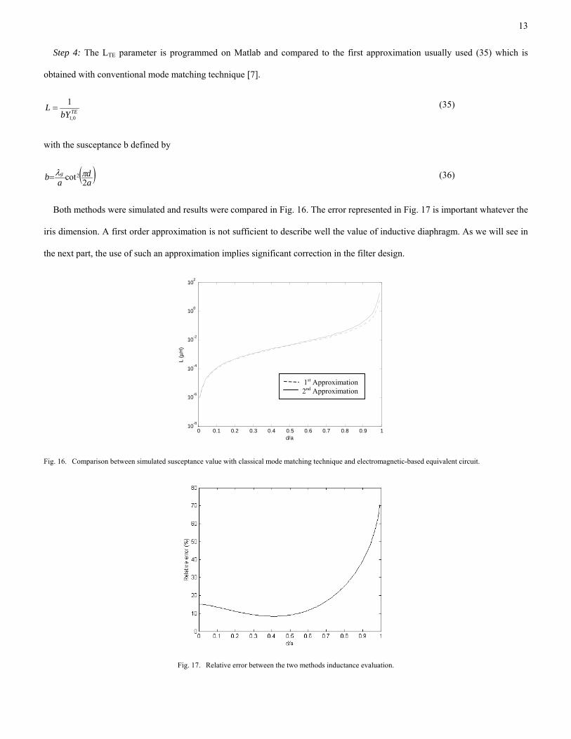
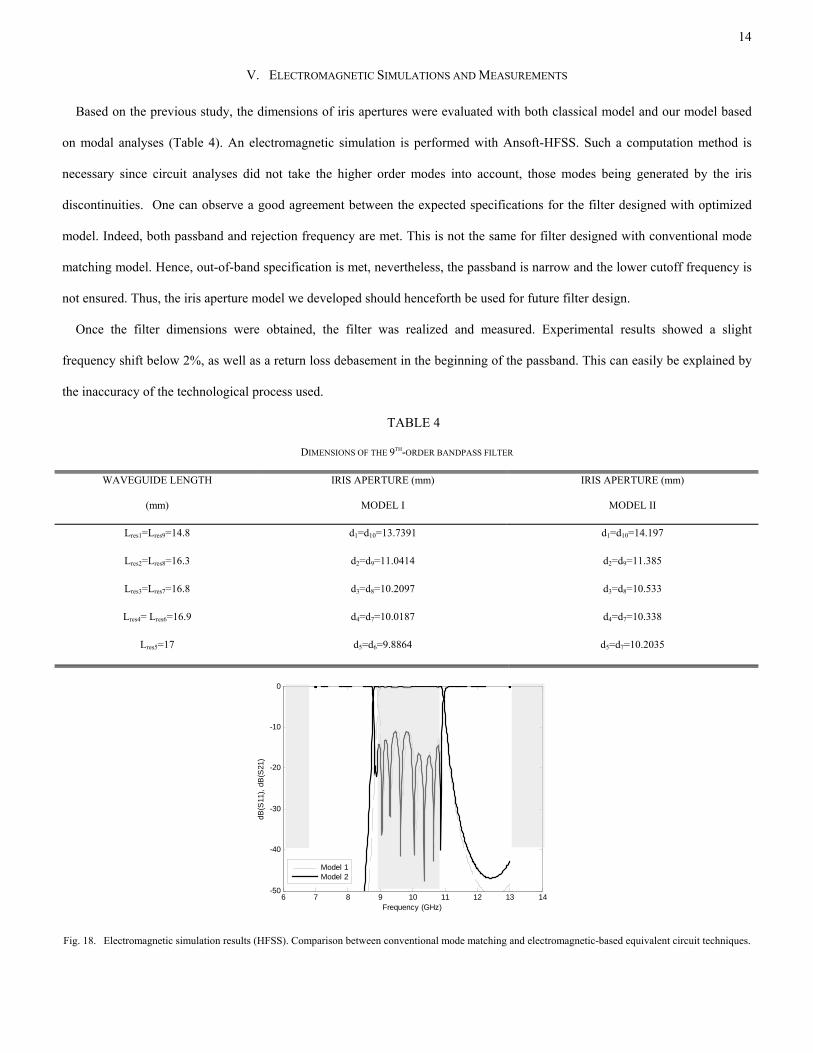
Both methods were simulated and results were compared in Fig. 16. The error represented in Fig. 17 is important whatever the
iris dimension. A first order approximation is not sufficient to describe well the value of inductive diaphragm. As we will see in
the next part, the use of such an approximation implies significant correction in the filter design.
0 0.1 0.2 0.3 0.4 0.5 0.6 0.7 0.8 0.9 110-8
10-6
10-4
10-2
100
102
d/a
L (µ
H)
1st Approximation2nd Approximation
Fig. 16. Comparison between simulated susceptance value with classical mode matching technique and electromagnetic-based equivalent circuit.
Fig. 17. Relative error between the two methods inductance evaluation.
14
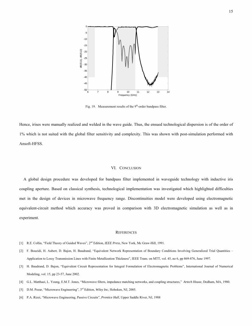
V. ELECTROMAGNETIC SIMULATIONS AND MEASUREMENTS
Based on the previous study, the dimensions of iris apertures were evaluated with both classical model and our model based
on modal analyses (Table 4). An electromagnetic simulation is performed with Ansoft-HFSS. Such a computation method is
necessary since circuit analyses did not take the higher order modes into account, those modes being generated by the iris
discontinuities. One can observe a good agreement between the expected specifications for the filter designed with optimized
model. Indeed, both passband and rejection frequency are met. This is not the same for filter designed with conventional mode
matching model. Hence, out-of-band specification is met, nevertheless, the passband is narrow and the lower cutoff frequency is
not ensured. Thus, the iris aperture model we developed should henceforth be used for future filter design.
Once the filter dimensions were obtained, the filter was realized and measured. Experimental results showed a slight
frequency shift below 2%, as well as a return loss debasement in the beginning of the passband. This can easily be explained by
the inaccuracy of the technological process used.
TABLE 4
DIMENSIONS OF THE 9TH-ORDER BANDPASS FILTER
WAVEGUIDE LENGTH
(mm)
IRIS APERTURE (mm)
MODEL I
IRIS APERTURE (mm)
MODEL II
Lres1=Lres9=14.8 d1=d10=13.7391 d1=d10=14.197
Lres2=Lres8=16.3 d2=d9=11.0414 d2=d9=11.385
Lres3=Lres7=16.8 d3=d8=10.2097 d3=d8=10.533
Lres4= Lres6=16.9 d4=d7=10.0187 d4=d7=10.338
Lres5=17 d5=d6=9.8864 d5=d7=10.2035
6 7 8 9 10 11 12 13 14-50
-40
-30
-20
-10
0
Frequency (GHz)
dB(S
11),
dB(S
21)
Model 1Model 2
Fig. 18. Electromagnetic simulation results (HFSS). Comparison between conventional mode matching and electromagnetic-based equivalent circuit techniques.
15
6 7 8 9 10 11 12 13 14-50
-45
-40
-35
-30
-25
-20
-15
-10
-5
0
Frequency (GHz)
dB(S
11),
dB(S
12)
Fig. 19. Measurement results of the 9th-order bandpass filter.
Hence, irises were manually realized and welded in the wave guide. Thus, the ensued technological dispersion is of the order of
1% which is not suited with the global filter sensitivity and complexity. This was shown with post-simulation performed with
Ansoft-HFSS.
VI. CONCLUSION
A global design procedure was developed for bandpass filter implemented in waveguide technology with inductive iris
coupling aperture. Based on classical synthesis, technological implementation was investigated which highlighted difficulties
met in the design of devices in microwave frequency range. Discontinuities model were developed using electromagnetic
equivalent-circuit method which accuracy was proved in comparison with 3D electromagnetic simulation as well as in
experiment.
REFERENCES
[1] R.E. Collin, “Field Theory of Guided Waves”, 2nd Edition, IEEE Press, New York, Mc Graw-Hill, 1991.
[2] F. Bouzidi, H. Aubert, D. Bajon, H. Baudrand, “Equivalent Network Representation of Boundary Conditions Involving Generalized Trial Quantities –
Application to Lossy Transmission Lines with Finite Metallization Thickness”, IEEE Trans. on MTT, vol. 45, no 6, pp 869-876, June 1997.
[3] H. Baudrand, D. Bajon, “Equivalent Circuit Representation for Integral Formulation of Electromagnetic Problems”, International Journal of Numerical
Modeling, vol. 15, pp 23-57, June 2002.
[4] G.L. Matthaei, L. Young, E.M.T. Jones, “Microwave filters, impedance matching networks, and coupling structures,” Artech House, Dedham, MA, 1980.
[5] D.M. Pozar, “Microwave Engineering”, 3rd Edition, Wiley Inc, Hoboken, NJ, 2005.
[6] P.A. Rizzi, “Microwave Engineering, Passive Circuits”, Prentice Hall, Upper Saddle River, NJ, 1988

16
[7] R.E. Collin, “Foundation of Microwaves Engineering”, 2nd Edition, IEEE Press, Mc Graw-Hill , New York, , 1992.