Design of Substrate Integrated Waveguide …jbornema/Conferences/161-15gsmm-sktlb.pdfDesign of...
3
Design of Substrate Integrated Waveguide Components Jan Schorer 1 , Zamzam Kordiboroujeni 1 , Farzaneh Taringou 2 , Lisa Locke 1 , and Jens Bornemann 1 1 Department of Electrical & Computer Engineering, University of Victoria, BC, Canada 2 ACE − Advanced Computational Engineering GmbH, Munich, Germany Abstract—This paper presents an overview of substrate integrated waveguide (SIW) design activities at the University of Victoria. Mode-matching techniques (MMTs) are employed to facilitate the design of planar SIW circuits as well as surface mounted waveguide (SMW) components. Active component integration and antenna design employ commercially available field solvers. Each category is highlighted by a sample component, comparing theoretical and/or measured results for K-band applications. Good agreement between simulated and experimental results is observed. Keywords—substrate integrated waveguide; surface mounted waveguide; mode-matching technique; computer-aided design; low-noise amplifier; printed-circuit antennas. I. INTRODUCTION Over the past decade, substrate integrated waveguide (SIW) circuitry has developed into a mature technology and has proven to be a promising alternative to conventional all-metal waveguides for the design of microwave and millimeter-wave communication systems components [1]. In this technology, relatively low-loss and high-Q waveguide structures are realized as highly integrated planar microwave structures with compact size, at low cost, and with low interference due to its shielded environment [2]. However, SIW designs for an all-encompassing technology experience several bottlenecks. First, passive SIW components are usually designed with commercially available field solvers such as CST and HFSS. Even for a good initial design based on all-dielectric waveguides, the transition to SIW requires fine optimization that takes a relatively long time and thus makes the final design stage cumbersome. Secondly, for SIW filter and multiplexer applications, the Q factor of several hundred is not compatible with that of metal waveguide which is in the thousands. Empty SIW cavities are proposed in [3] to reduce losses, but the resonator height is limited to that of the substrate. Thirdly, the integration of active components for amplifier, mixer and automatic gain control operations can be considered to be still in its infancy. And fourthly, SIW antennas on high-permittivity substrates for densely spaced arrays need to be designed to make SIW technology amenable to communications and radio astronomy applications. _______________________________________________________________ This work was supported by the National Science and Engineering Research Council (NSERC) of Canada and the TELUS Grant in Wireless Communications. Therefore, to remedy some of the above-mentioned problems, this paper presents a number of solutions which have been developed at the University of Victoria. Due to space limitations, only one example for each of the four areas discussed above will be presented. II. EXAMPLES OF SIW COMPONENTS DESIGN A. Mode-Matching Design of Passive SIW Circuits Several contributions have been made towards the modeling and design of passive SIW circuits. The centerpiece of our new approach is a full-wave mode-matching technique (MMT) that allows a fast and accurate analysis of substrate- integrated waveguide components with rectangular/square via holes. Models for several discontinuities are discussed which include microstrip transitions [4] and a loss analysis [5]. For transferring an all-dielectric rectangular waveguide designs to SIW technology, the equivalent waveguide width of the SIW is of fundamental importance [6]. It makes the many well-developed waveguide synthesis procedures applicable for the design of SIW components. As many SIW circuits are fabricated in standard PCB technologies involving circular via holes, equivalence between square and circular vias has been established and tested in demanding SIW filter, diplexer, coupler and power divider applications. Based on this equivalence, any circular via with diameter d can be approximated by a square via with side length l that is arithmetic mean of the side lengths of the inscribed and circumscribed squares of the circular via [7]. Fig. 1 shows an example of a K-band T-junction on RT/duroid 6002 substrate and a comparison between the MMT, CST and experimental results. Measured insertion losses are 3.88 dB and 4.28 dB compared with 2.39 dB and 2.46 dB, respectively, in the CST simulations. The minimum measured return losses in the two bands are 18.13 dB and 16.9 dB, respectively, compared to 23.4 dB and 21.3 dB in the simulation. Due to fabrication restrictions, the via diameter has been slightly changed which causes the measured data to have a slight frequency shift towards higher frequencies compared to the MMT and simulated data. Otherwise, the measured data confirms the validity of the proposed MMT approach for the analysis and design of SIW components.
Transcript of Design of Substrate Integrated Waveguide …jbornema/Conferences/161-15gsmm-sktlb.pdfDesign of...

Design of Substrate Integrated Waveguide Components
Jan Schorer1, Zamzam Kordiboroujeni1, Farzaneh Taringou2, Lisa Locke1, and Jens Bornemann1 1 Department of Electrical & Computer Engineering, University of Victoria, BC, Canada
2 ACE − Advanced Computational Engineering GmbH, Munich, Germany
Abstract—This paper presents an overview of substrate
integrated waveguide (SIW) design activities at the University of Victoria. Mode-matching techniques (MMTs) are employed to facilitate the design of planar SIW circuits as well as surface mounted waveguide (SMW) components. Active component integration and antenna design employ commercially available field solvers. Each category is highlighted by a sample component, comparing theoretical and/or measured results for K-band applications. Good agreement between simulated and experimental results is observed.
Keywords—substrate integrated waveguide; surface mounted waveguide; mode-matching technique; computer-aided design; low-noise amplifier; printed-circuit antennas.
I. INTRODUCTION Over the past decade, substrate integrated waveguide (SIW)
circuitry has developed into a mature technology and has proven to be a promising alternative to conventional all-metal waveguides for the design of microwave and millimeter-wave communication systems components [1]. In this technology, relatively low-loss and high-Q waveguide structures are realized as highly integrated planar microwave structures with compact size, at low cost, and with low interference due to its shielded environment [2].
However, SIW designs for an all-encompassing technology experience several bottlenecks. First, passive SIW components are usually designed with commercially available field solvers such as CST and HFSS. Even for a good initial design based on all-dielectric waveguides, the transition to SIW requires fine optimization that takes a relatively long time and thus makes the final design stage cumbersome. Secondly, for SIW filter and multiplexer applications, the Q factor of several hundred is not compatible with that of metal waveguide which is in the thousands. Empty SIW cavities are proposed in [3] to reduce losses, but the resonator height is limited to that of the substrate. Thirdly, the integration of active components for amplifier, mixer and automatic gain control operations can be considered to be still in its infancy. And fourthly, SIW antennas on high-permittivity substrates for densely spaced arrays need to be designed to make SIW technology amenable to communications and radio astronomy applications. _______________________________________________________________
This work was supported by the National Science and Engineering Research Council (NSERC) of Canada and the TELUS Grant in Wireless Communications.
Therefore, to remedy some of the above-mentioned problems, this paper presents a number of solutions which have been developed at the University of Victoria. Due to space limitations, only one example for each of the four areas discussed above will be presented.
II. EXAMPLES OF SIW COMPONENTS DESIGN
A. Mode-Matching Design of Passive SIW Circuits Several contributions have been made towards the
modeling and design of passive SIW circuits. The centerpiece of our new approach is a full-wave mode-matching technique (MMT) that allows a fast and accurate analysis of substrate-integrated waveguide components with rectangular/square via holes. Models for several discontinuities are discussed which include microstrip transitions [4] and a loss analysis [5].
For transferring an all-dielectric rectangular waveguide designs to SIW technology, the equivalent waveguide width of the SIW is of fundamental importance [6]. It makes the many well-developed waveguide synthesis procedures applicable for the design of SIW components.
As many SIW circuits are fabricated in standard PCB technologies involving circular via holes, equivalence between square and circular vias has been established and tested in demanding SIW filter, diplexer, coupler and power divider applications. Based on this equivalence, any circular via with diameter d can be approximated by a square via with side length l that is arithmetic mean of the side lengths of the inscribed and circumscribed squares of the circular via [7].
Fig. 1 shows an example of a K-band T-junction on RT/duroid 6002 substrate and a comparison between the MMT, CST and experimental results. Measured insertion losses are 3.88 dB and 4.28 dB compared with 2.39 dB and 2.46 dB, respectively, in the CST simulations. The minimum measured return losses in the two bands are 18.13 dB and 16.9 dB, respectively, compared to 23.4 dB and 21.3 dB in the simulation. Due to fabrication restrictions, the via diameter has been slightly changed which causes the measured data to have a slight frequency shift towards higher frequencies compared to the MMT and simulated data. Otherwise, the measured data confirms the validity of the proposed MMT approach for the analysis and design of SIW components.
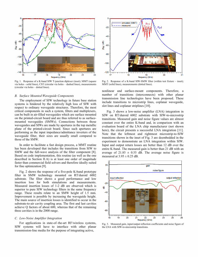
Fig. 1. Response of a K-band SIW T-junction diplexer (inset); MMT (square via holes - solid lines), CST (circular via holes – dashed lines), measurements (circular via holes – dotted lines).
B. Surface Mounted Waveguide Components The employment of SIW technology in future base station
systems is hindered by the relatively high loss of SIW with respect to ordinary waveguide structures. Therefore, the most critical components in such a system, filters and multiplexers, can be built in air-filled waveguides which are surface mounted on the printed-circuit board and are thus referred to as surface-mounted waveguides (SMWs). Connections between those waveguides and SIWs are made by apertures in the top metallic plane of the printed-circuit board. Since such apertures are performing as the input impedance/admittance inverters of the waveguide filter, their sizes are usually small compared to those of the SMW.
In order to facilitate a fast design process, a MMT routine has been developed that includes the transitions from SIW to SMW and the full-wave analysis of the filter component [8]. Based on code implementation, this routine (as well as the one described in Section II.A) is at least one order of magnitude faster than commercial field solvers and therefore ideally suited for fine optimization [9].
Fig. 2 shows the response of a five-pole K-band prototype filter in SMW technology mounted on RT/duroid 6002 substrate. The filter shows a good performance and low insertion loss for both simulations and measurements. Measured insertion losses of 1-2 dB are observed which is superior to pure SIW technology filters in the same frequency range. These results relate to an SMW height of 1.5 mm. Improvement is possible by increasing the waveguide height. The main source of insertion losses is identified to occur in the substrate-to-air cavity coupling area. The first and last cavities achieve Q factors of about 600, whereas that of the remaining three cavities is in the 2000 range.
C. Low-Noise Amplifier Integration For applications in state-of–the-art RF/wireless systems,
SIW systems will have to interface with other planar transmission-line media for the purpose of integrating active,
Fig. 2. Response of a K-band SIW-SMW filter (within test fixture – inset); MMT (solid lines), measurements (dotted lines).
nonlinear and surface-mount components. Therefore, a number of transitions (interconnects) with other planar transmission line technologies have been proposed. These include transitions to microstrip lines, coplanar waveguide, slot lines and coplanar striplines [10].
Fig. 3 shows a low-noise amplifier (LNA) integration in SIW on RT/duroid 6002 substrate with SIW-to-microstrip transitions. Measured gain and noise figure values are almost constant over the entire K-band and, in comparison with an evaluation board of the LNA chip manufacturer (not shown here), the circuit presents a successful LNA integration [11]. Note that the leftmost and rightmost microstrip-to-SIW transitions shown in the inset of Fig. 3 are deembedded in the experiment to demonstrate an LNA integration within SIW. Input and output return losses are better than 12 dB over the entire K-band. The measured gain is better than 21 dB with an average of 21.85 ± 0.55 dB. The average noise figure is measured at 3.95 ± 0.25 dB.
Fig. 3. Measured gain, input/output reflection coefficients and noise figure of the LNA with SIW-to-microstrip transitions.

D. SIW Antenna Antenna integration in SIW is mostly concerned with
antipodal tapered slot antennas (ATSAs). While quite a few of such antennas with SIW feeds have been proposed, they are usually manufactured on low-permittivity substrates.
However, in order to facilitate ATSA arrays with dense spacing requirements (usually a half free-space wavelength center-to-center), such antennas need to be realized on high-permittivity substrates in which part of the substrate in the antenna taper is cut out to satisfy the effective thickness condition, e.g. [12]. The design, which includes corrugation for cross-polarization reduction, is performed as a parametric study involving commercially available field solvers [13].
Fig. 4 shows a photograph and radiation patterns of the K-band prototype at 22 GHz [14]. Agreement between CST simulations and measurements over the main beam are very good. Simulated and measured cross-polarization responses are below design goal of 20 dB. The input return loss (with the microstrip-to-SIW transition deembedded) is better than 10 dB over most of the K-band, and better that 8 dB up to 26.5 GHz. Note that similar values, with slightly improved return loss but slightly reduced cross polarization have been achieved for a 90-120 GHz ATSA on low-permittivity substrate [12].
Fig. 4. ATSA prototype and radiation patterns at 22 GHz; CST (solid lines), measurements (dotted lines).
III. CONCLUSIONS An overview of selected SIW design activities at the
University of Victoria is presented. Examples include passive
SIW circuits, SMW components, LNA integration and antennas. Good experimental performance of all components validates the design approaches.
REFERENCES [1] M. Bozzi, L. Perregrini, K. Wu, and P. Arcioni, “Current and future
research trends in substrate integrated waveguide technology,” Radioengineering, vol. 18, pp. 201-209, June 2009.
[2] M. Bozzi, A. Georgiadis, and K. Wu, “Review of substrate-integrated waveguide circuits and antennas,” IET Microw. Antennas Propag., vol. 5, pp. 909–920, June 2011.
[3] A. Belenguer, H. Esteban, and V. Boria, “Novel empty substrate integrated waveguide for high-performance microwave integrated circuits,” IEEE Trans. Microw. Theory Tech., vol. 62, pp. 832–839, Apr. 2014.
[4] J. Bornemann, F. Taringou and Z. Kordiboroujeni, “A mode-matching approach for the analysis and design of substrate-integrated waveguide components,” Frequenz, vol. 65, pp. 287–292, Sep. 2011.
[5] Z. Kordiboroujeni and J. Bornemann, “Mode matching design of substrate integrated waveguide diplexers,” IEEE MTT-S Int. Microwave Symp. Dig., pp. 1-3, Seattle, USA, June 2013..
[6] Z. Kordiboroujeni and J. Bornemann, “Designing the width of substrate integrated waveguide structures,” IEEE Microw. Wireless Compon. Lett., Vol. 23, pp. 518-520, Oct. 2013.
[7] Z. Kordiboroujeni and J. Bornemann, “Mode-matching analysis and design of substrate integrated waveguide T-junction diplexer and corner filter,” Int. J. Numer. Model., 2015, in press.
[8] J. Schorer and J. Bornemann, “Mode-matching analysis for double-layered substrate integrated and rectangular waveguide filter technology,” Proc. Int. Conf. Computational Electromagnetics (ICCEM), pp. 158-160, Hong Kong, Feb. 2015.
[9] J. Schorer, J. Bornemann, and U. Rosenberg, “Comparison of surface mounted high quality filters for combination of substrate integrated and waveguide technology,” Proc. Asia-Pacific Microw. Conf., pp. 929-931, Sendai, Japan, Nov. 2014.
[10] F. Taringou, D. Dousset, J. Bornemann and K. Wu, “Substrate-integrated waveguide transitions to planar transmission-line technologies,” IEEE MTT-S Int. Microw. Symp. Dig., pp.1-3, Montreal, Canada, June 2012.
[11] F. Taringou, J. Bornemann, and K. Wu, “Broadband coplanar-waveguide and microstrip low-noise amplifier hybrid integrations for K-band substrate integrated waveguide applications on low-permittivity substrate,” IET Microw. Antennas Propag., vol. 8, pp. 99-103, Jan. 2014.
[12] F. Taringou, D. Dousset, J. Bornemann and K. Wu, "Broadband CPW feed for millimeter-wave SIW-based antipodal linearly tapered slot antennas", IEEE Trans. Antennas Propagat., vol. 61, pp. 1756-1762, Apr. 2013.
[13] L. Locke, J. Bornemann and S. Claude, "Substrate integrated waveguide-fed tapered slot antenna with smooth performance characteristics over an ultra-wide bandwidth", ACES .J, vol. 28, pp. 454-462, May 2013.
[14] L. Locke, S. Claude, J. Bornemann, D. Henke, J. Di Francesco, F. Jiang, D. Garcia, I. Wevers and P. Niranjanan, “KPAF (K-band phased array feed) instrument concept,” Proc. SPIE Millimeter, Submillimeter, and Far-Infrared Detectors and Instrumentation for Astronomy VII, pp. 91531Z-1 - 91531Z-11, Montreal, Canada, June 2014.