DESIGN OF LOW PHASE NOISE VERY HIGH FREQUENCY (VHF) …
57
DESIGN OF LOW PHASE NOISE VERY HIGH FREQUENCY (VHF) LOW BAND VOLTAGE CONTROLLED OSCILLATOR (VCO) FOR TRANSCEIVER APPLICATION by YEAP KIM HUAT Thesis submitted in fulfilment of the requirements for the degree of Masters of Science September 2011 brought to you by CORE View metadata, citation and similar papers at core.ac.uk provided by Repository@USM
Transcript of DESIGN OF LOW PHASE NOISE VERY HIGH FREQUENCY (VHF) …

DESIGN OF LOW PHASE NOISE VERY HIGH FREQUENCY (VHF) LOW BAND VOLTAGE CONTROLLED OSCILLATOR (VCO) FOR
TRANSCEIVER APPLICATION
by
YEAP KIM HUAT
Thesis submitted in fulfilment of the requirements for the degree of Masters of Science
September 2011
brought to you by COREView metadata, citation and similar papers at core.ac.uk
provided by Repository@USM
DECLARATION
I hereby declare that the work in this thesis is my own except for quotations and
summaries which have been duly acknowledged.
5th September 2011 YEAP KIM HUAT
S-LM0403
ii
AKNOWLEDGEMENT
It has been a great honor to be granted the opportunity to undergo my
postgraduate research in School of Electronic and Electrical Engineering of
Universiti Sains Malaysia.
First and foremost, I would like to dedicate my sincerest acknowledgement
towards my supervisor, Associate Professor Dr. Widad Ismail, for her invaluable
guidance and advises throughout my research. As a part-time researcher, my session
in meeting up with my supervisor has not been much often, but the inputs she
provided during every session have been very fruitful. In times of difficulties faced
during my research, there is no other but only my supervisor that I could refer to, in
which I really feel blessed about. With her vast knowledge and experience in the
research communication field, her advices have continuously helped me channeled
through the challenges I encountered.
My earnest gratitude to my parents, my twin brother, my sister in law, my
wife, and my daughter, weighs no lesser. The sophisticated journey in striving
through the research has been rather enduring. I have to admit that I almost cross the
boundary of giving up, have it not for the undivided and consistent support from
them. I could not but feel grateful and touched, when my negligence to them was
returned by their love and motivation, which turn out to be the bank of strength for
me to navigate through all hindrances I faced in my research.
No word could express the deep gratitude that blossoms in my heart. THANK
YOU VERY MUCH!
iii

TABLE OF CONTENTS
PAGE
DECLARATION ii
AKNOWLEDGEMENT iii
TABLE OF CONTENTS iv
LIST OF TABLES xi
LIST OF FIGURES xiv
LIST OF ABBREVIATIONS xxviii
ABSTRAK xxxii
ABSTRACT xxxiii
CHAPTER 1 INTRODUCTION 1
1.1 Background 1
1.2 Applications of VHF Low Band 2
1.3 Advantages of VHF Low Band 3
1.3.1 Precise Transmission 3
1.3.2 Extensive Coverage 4
1.3.3 Ample Spectrum Availability 4
1.3.4 Exemption from Narrow Band Requirements 4
1.4 Problem Statement 5
1.5 Research Objectives 6
1.6 Requirements 7
1.7 Research Scopes and Limitations 10
1.8 Research Contribution 11
iv

1.9 Thesis Organization 12
CHAPTER 2 LITERATURE SURVEY 13
2.0 Introduction 13
2.1 Noise 13
2.1.1 Thermal Noise 14
2.1.2 Shot Noise 15
2.1.3 Flicker Noise 16
2.2 Phase Noise 17
2.2.1 Leeson’s Model 20
2.2.2 Linear Time Invariant (LTI) Model 23
2.2.3 Lee and Hajimiri’s Model 28
2.2.4 Samori’s Model 33
2.2.5 Demir’s Model 41
2.3 Existing VCO Phase Noise Improvement Techniques 44
2.3.1 High Q Resonant Circuit 44
2.3.2 Selection of Oscillator Device 45
2.3.3 Increasing Area of Transistor 45
2.3.4 Sufficient Oscillator Power Output 46
2.3.5 Sufficient Feedback Level 46
2.3.6 Increase Core Current 46
2.3.7 Power Line Rejection 47
2.3.8 Filtering at Steering Line 48
2.3.9 Capacitive Filtering at The Tail Current Source 49
2.3.10 LC Filtering Technique 50
v

2.3.11 Remove Tail Current Source 51
2.3.12 Reduce VCO Sensitivity Kv by Switched Capacitors 51
2.3.13 Differential Steering Voltage Control 53
2.4 Previous Works 54
2.5 Summary 55
CHAPTER 3 RESEARCH METHODOLOGY 57
3.1 Introduction 57
3.2 Design Methodology 57
3.3 VHF Low Band VCO Block Design 60
3.4 Oscillator Design and Mathematical Model Derivations 61
3.5 ADS Overview 70
3.5.1 Lump Component Model 70
3.5.2 RF Component Model 71
3.5.3 Momentum Component Model 71
3.6 PCB Layout and Momentum Model 72
3.7 Components Selection and Design Configuration for Low Phase 81
Noise
3.7.1 Varactor Diode 81
3.7.2 Back-to-Back Varactor Diode 85
3.7.3 Low Noise Bypass Capacitor 86
3.7.4 RF Bypass Capacitor 86
3.7.5 RF Choke 87
3.7.6 Ferrite Bead 89
3.7.7 JFET Transistor 90
vi

3.7.8 Low Noise Biasing Design 92
3.7.9 Linearizing Inductor Design 93
3.7.10 Schottky Diodes AGC Design 97
3.8 Test and Measurement Methodology 97
3.8.1 S-Parameter Measurement Methodology 97
3.8.2 VCO Parametric Test Methodology 98
3.8.2.1 Frequency Response, Guard Band, Sensitivity, 99
Power Level Test
3.8.2.2 Phase Noise Test 100
3.8.2.3 Second Harmonics Output and Feedback Power 101
Test
3.8.2.4 Hum and Noise Test 102
3.9 Summary 103
CHAPTER 4 DESIGN AND SIMULATION 104
4.1 Introduction 104
4.2 Oscillator Design 104
4.2.1 Rx Oscillator Calculation 107
4.2.2 Rx Oscillator Lump Component Model Simulation 108
4.2.3 Rx Oscillator RF Component Model Simulation 114
4.2.4 Rx Oscillator Momentum Co-Simulation 119
4.2.5 Tx Oscillator Calculation 123
4.2.6 Tx Oscillator Lump Component Model Simulation 124
4.2.7 Tx Oscillator RF Component Model Simulation 128
4.2.8 Tx Oscillator Momentum Co-Simulation 133
vii

4.3 VCO Buffer and Pad Attenuator Design 137
4.3.1 Rx VCO Buffer with Pad Attenuator Lump Component 137
Model Simulation
4.3.2 Rx VCO Buffer with Pad Attenuator RF Component 140
Model Simulation
4.3.3 Rx VCO Buffer with Pad Attenuator Momentum Co- 143
Simulation
4.3.4 Tx VCO Buffer with Pad Attenuator Lump Component 146
Model Simulation
4.3.5 Tx VCO Buffer with Pad Attenuator RF Component 149
Model Simulation
` 4.3.6 Tx VCO Buffer with Pad Attenuator Momentum Co- 152
Simulation
4.4 Pre-Mixer Filter Design 155
4.4.1 Pre-Mixer Filter Calculation 155
4.4.2 Pre-Mixer Filter Lump Component Model Simulation 156
4.4.3 Pre-Mixer Filter RF Component Model Simulation 157
4.4.4 Pre-Mixer Filter Momentum Co-Simulation 158
4.5 VCO Design 159
4.5.1 Rx VCO RF Component Model Simulation 160
4.5.2 Rx VCO Momentum Co-Simulation 164
4.5.3 Tx VCO RF Component Model Simulation 168
4.5.4 Tx VCO Momentum Co-Simulation 172
4.6 Phase Noise Discussion 176
4.7 Summary 178
viii
CHAPTER 5 RESULTS AND DISCUSSIONS 179
5.1 Introduction 179
5.2 Measurement Results and Discussion 180
5.2.1 Rx VCO Buffer with Pad Attenuator Measurement Results 180
and Analysis
5.2.2 Pre-Mixer Filter Measurement Result and Analysis 183
5.2.3 Rx VCO Measurement Results and Analysis 184
5.2.4 Tx VCO Buffer with Pad Attenuator Measurement Results 188
and Analysis
5.2.5 Tx VCO Measurement Results and Analysis 191
5.3 Competitive Analysis with Previous Works 195
5.4 Summary 195
CHAPTER 6 CONCLUSIONS AND FUTURE WORKS 197
6.1 Conclusions 197
6.2 Future Works 198
LIST OF PUBLICATIONS 200
REFERENCES 201
APPENDIX A: ADS SIMULATOR
APPENDIX B: TOSHIBA HN1V02H VARACTOR DIODE DATASHEET
APPENDIX C: TOSHIBA HN1V02H VARACTOR DIODE SPICE DATA
APPENDIX D: ON SEMI MMBFU310LT1 JFET TRANSISTOR
DATASHEET
APPENDIX E: PAD ATTENUATOR SIMULATION
ix
APPENDIX F: VHF LOW BAND VCO MEASURED PERFORMANCE AT
EXTREME TEMPERATURE
x
LIST OF TABLES
PAGE
Table 1.1 Phase noise specifications of VCO 7
Table 1.2 ACR, ACP, Hum & Noise specifications (TIA, 2002) 8
Table 1.3 Design specifications of Rx VCO 9
Table 1.4 Design specifications of Tx VCO 9
Table 2.1 Previous works comparison for VCO operating in VHF 55
range
Table 3.1 Electrical characteristics for HN1V02H 83
Table 3.2 Simulated varactor capacitance for the desired resonance 84
frequency
Table 3.3 On characteristics of MMBFU310LT1 91
Table 3.4 Summarized comparison of simulated capacitance for 96
varactor network with RFC, to linearizing inductor of
820 nH (a) and linearizing inductor of 1.2 μH (b)
Table 4.1 Net capacitance of varactor diodes (a), inductor selection 107
(b), and capacitors selection (c), for Rx oscillator design
Table 4.2 Calculated Rx oscillation frequency from the selected 108
components value
Table 4.3 Rx oscillator performance simulated using lump 113
component model
Table 4.4 Rx oscillator performance simulated using RF component 118
model
Table 4.5 Rx oscillator performance simulated using Momentum 122
xi

co-simulation model
Table 4.6 Net capacitance of varactor diodes (a), inductor selection 123
(b), and capacitors selection (c), for Tx oscillator design
Table 4.7 Calculated Tx oscillation frequency from the selected 123
component values
Table 4.8 Tx oscillator performance simulated using lump 128
component model
Table 4.9 Tx oscillator performance simulated using RF component 132
model
Table 4.10 Tx oscillator performance simulated using Momentum 136
co-simulation model
Table 4.11 Parts reference for Rx VCO 161
Table 4.12 Rx VCO performance simulated using RF component 163
model
Table 4.13 Rx VCO performance simulated using Momentum 167
co-simulation model
Table 4.14 Parts reference for Tx VCO 169
Table 4.15 Tx VCO performance simulated using RF component 171
model
Table 4.16 Tx VCO performance simulated using Momentum 175
co-simulation model
Table 4.17 Rx oscillator phase noise comparison between low phase 177
noise design and conventional design
Table 4.18 Tx oscillator phase noise comparison between low phase 177
noise design and conventional design
xii

Table 5.1 Rx VCO measured performance 184
Table 5.2 Tx VCO measured performance 191
Table 5.3 Phase noise comparison with other publications 195
xiii

LIST OF FIGURES
PAGE
Figure 1.1 VCO used as LO in Rx and RF source in Tx (Zhu, 2005) 1
Figure 1.2 Block diagram of PLL (Zhu, 2005) 2
Figure 2.1 Spectral density of flicker noise versus (vs.) frequency 17
Figure 2.2 General RTN characteristic 17
Figure 2.3 An ideal oscillating signal in time domain and frequency 18
domain
Figure 2.4 A practical oscillating signal in time domain and frequency 18
domain
Figure 2.5 Phase noise referenced to the carrier frequency power in 19
1 Hz bandwidth
Figure 2.6 Effect of phase noise onto the wanted signal 20
Figure 2.7 SSB oscillator phase noise output spectrum 22
Figure 2.8 One-port negative resistance oscillator with noise current 23
in the tank
Figure 2.9 Noise shaping in oscillators 25
Figure 2.10 Tank circuit includes the series parasitic resistance, Rl and 25
Rc, as well as the parallel parasitic resistance, Rp
Figure 2.11 Impulse effects on a sinusoidal signal (Hajimiri and Lee, 28
1998)
Figure 2.12 ISF of an LC oscillator (Hajimiri and Lee, 1998) 29
Figure 2.13 Input voltage (top), output current (middle), and 35
transconductance (bottom) of a bipolar differential pair
xiv

biased by 1 mA tail current
Figure 2.14 Dependence of AM and PM transconductance of a BJT 38
(left) and MOS (right) pairs as a function of the amplitude
of the input signal
Figure 2.15 Oscillator trajectories 42
Figure 2.16 Base and collector uncoupling with capacitor (Samori and 47
Laicaita, 1998)
Figure 2.17 Capacitive filtering at the tail current source (Muer et al., 49
2000)
Figure 2.18 Tail-biased oscillator with noise filter 50
Figure 2.19 Switched capacitor array design VCO 52
Figure 2.20 Set Kv curves by selecting MIM capacitors and tuning 52
varactors
Figure 2.21 The differential steering voltage control design 53
Figure 2.22 The complementary capacitance to steering voltage 54
characteristic
Figure 3.1 Design flow of low phase noise VCO for VHF low band 59
Figure 3.2 Tx and Rx VCO block design 61
Figure 3.3 Common-gate FET Colpitts oscillator topology 62
Figure 3.4 Common-gate FET Colpitts oscillator topologies in terms 63
of impedance block (a) and small signal block model (b)
Figure 3.5 Close loop block model of the VCO 69
Figure 3.6 Open loop block model of the VCO 69
Figure 3.7 Summary of full-wave analysis (a) and quasi-static analysis 72
(b)
xv
Figure 3.8 Layout layer structure and thickness 75
Figure 3.9 Setting up the Hitachi halogen-free FR-4 substrate 75
Figure 3.10 Setting up the copper layer of the PCB 76
Figure 3.11 Via sheet in between the top conductor layer and the inner 77
ground plane
Figure 3.12 Tx oscillator layout on the top layer (a) while the Rx 78
oscillator layout on the bottom layer (b)
Figure 3.13 Rx buffer and pad attenuator layout on the top layer (a) 78
while Tx buffer and pad attenuator layout are on the
bottom layer (b)
Figure 3.14 Top (a) and bottom (b) layout of the Rx pre-mixer filter 78
Figure 3.15 Setup control for mesh computation 80
Figure 3.16 EM model of the oscillator layout (a), the buffer and pad 80
attenuator layout (b), as well as the pre-mixer filter layout
(c)
Figure 3.17 Component model of the oscillator layout (a), the buffer 81
and pad attenuator layout (b), as well as the pre-mixer
filter layout (c)
Figure 3.18 Simulation circuit for the HN1V02H capacitance, where 84
the varactor is modeled base on the spice data from
Toshiba
Figure 3.19 Varactor capacitance across the steering voltage, at 84
30 MHz to 57 MHz
Figure 3.20 Back-to-back varactor configuration 85
Figure 3.21 Forward biased and reverse biased regions of the varactor 85
xvi

Figure 3.22 simulation setup for C1608X7R1H103K component 87 21S
model (a) as well as simulation result 21S
Figure 3.23 simulation setup for 1812CS-333XJLC component 88 11Z
model (a) and 1812CS-273XJLC component model (b) as
well as simulation result (c) 11Z
Figure 3.24 simulation setup for the FBMH4525-HM162NT 89 11Z
component model (a) as well as simulation result (b) 11Z
Figure 3.25 MMBFU310LT1 forward transconductance vs. gate-source 91
voltage plot
Figure 3.26 MMBFU310LT1 junction capacitance vs. gate-source 91
voltage plot
Figure 3.27 MMBFU310LT1 common-gate S-parameter vs. frequency 92
plot
Figure 3.28 Low noise biasing circuit design 92
Figure 3.29 Linearizing inductor connected to the back-to-back 93
varactors
Figure 3.30 Simulation setup for the Rx VCO varactor network 95
connected to RFC (a) and 820 nH linearizing inductor (c);
Simulation setup for the Tx VCO varactor network
connected to RFC (b) and 1.2 uH linearizing inductor (d)
Figure 3.31 Comparison of the back-to-back varactor capacitance 96
connected with RFC, to that with linearizing inductor of
820 nH (a) and 1.2 μH (b)
Figure 3.32 ON Semi MMBD353LT1 Schottky diodes act as AGC to 97
the oscillator
xvii
Figure 3.33 S-parameter measurement setup 98
Figure 3.34 VCO parametric test setup 99
Figure 3.35 VCO frequency and sensitivity test setup 100
Figure 3.36 VCO output power and feedback power test setup 101
Figure 3.37 VCO hum & noise test setup 102
Figure 4.1 Oscillator design 105
Figure 4.2 Calculated Rx oscillator frequency response 108
Figure 4.3 Rx oscillator schematic designed using lump component 109
model
Figure 4.4 S-parameter simulator setup for Rx oscillator lump 110
component model
Figure 4.5 Rx oscillator open loop gain and phase shift plot for low 111
(a) and high (b) end of the band, simulated using lump
component model
Figure 4.6 HB simulator setup for Rx oscillator lump component 111
model
Figure 4.7 Rx oscillator frequency response simulated using lump 112
component model
Figure 4.8 Rx oscillator phase noise response simulated using lump 112
component model
Figure 4.9 Rx oscillator output power and second harmonics 113
simulated using lump component model
Figure 4.10 Rx oscillator schematic designed using RF component 115
model
Figure 4.11 S-parameter simulator setup for Rx oscillator RF 116
xviii

component model
Figure 4.12 Rx oscillator open loop gain and phase shift plot for low 116
(a) and high (b) end of the band, simulated using RF
component model
Figure 4.13 HB simulator setup for Rx oscillator RF component model 117
Figure 4.14 Rx oscillator frequency response simulated using RF 117
component model
Figure 4.15 Rx oscillator phase noise response simulated using RF 117
component model
Figure 4.16 Rx oscillator output power and second harmonics 118
simulated using RF component model
Figure 4.17 Rx oscillator schematic designed using Momentum co- 119
simulation model
Figure 4.18 Rx oscillator open loop gain and phase shift plot for low 120
(a) and high (b) end of the band, simulated using
Momentum co-simulation model
Figure 4.19 Rx oscillator frequency response simulated using 121
Momentum co-simulation model
Figure 4.20 Rx oscillator phase noise response simulated using 121
Momentum co-simulation model
Figure 4.21 Rx oscillator output power and second harmonics 122
simulated using Momentum co-simulation model
Figure 4.22 Calculated Tx oscillator frequency response 124
Figure 4.23 Tx oscillator schematic designed using lump component 125
model
xix

Figure 4.24 Tx oscillator open loop gain and phase shift plot for low 126
(a) and high (b) end of the band, simulated using lump
component model
Figure 4.25 Tx oscillator frequency response simulated using lump 126
component model
Figure 4.26 Tx oscillator phase noise response simulated using lump 126
component model
Figure 4.27 Tx oscillator output power and second harmonics 128
simulated using lump component model
Figure 4.28 Tx oscillator schematic designed using RF component 129
model
Figure 4.29 Tx oscillator open loop gain and phase shift plot for low 130
(a) and high (b) end of the band, simulated using RF
component model
Figure 4.30 Tx oscillator frequency response simulated using RF 131
component model
Figure 4.31 Tx oscillator phase noise response simulated using RF 131
component model
Figure 4.32 Tx oscillator output power and second harmonics 132
simulated using RF component model
Figure 4.33 Tx oscillator schematic designed using Momentum co- 133
simulation model
Figure 4.34 Tx oscillator open loop gain and phase shift plot for low 134
(a) and high (b) end of the band, simulated using
Momentum co-simulation model
xx

Figure 4.35 Tx oscillator frequency response simulated using 135
Momentum co-simulation model
Figure 4.36 Tx oscillator phase noise response simulated using 135
Momentum co-simulation model
Figure 4.37 Tx oscillator output power and second harmonics 136
simulated using RF component models
Figure 4.38 Schematic of Rx VCO buffer with pad attenuator designed 138
using lump component model
Figure 4.39 LSSP simulator setup for Rx VCO buffer with pad 138
attenuator using lump component model
Figure 4.40 Gain of Rx VCO buffer with pad attenuator simulated 139
using lump component model
Figure 4.41 Isolation of Rx VCO buffer with pad attenuator simulated 139
using lump component model
Figure 4.42 Stability plot of Rx VCO buffer with pad attenuator 140
Simulated using lump component model
Figure 4.43 Output return loss of Rx VCO buffer with pad attenuator 140
and buffer alone, simulated using lump component model
Figure 4.44 Schematic of Rx VCO buffer with pad attenuator designed 141
using RF component model
Figure 4.45 LSSP simulator setup for Rx VCO buffer with pad 141
attenuator using RF component model
Figure 4.46 Gain of Rx VCO buffer with pad attenuator simulated 142
using RF component model
Figure 4.47 Stability plot of Rx VCO buffer with pad attenuator 142
xxi
simulated using RF component model
Figure 4.48 Isolation of Rx VCO buffer with pad attenuator simulated 143
using RF component model
Figure 4.49 Output return loss of Rx VCO buffer with pad attenuator 143
and buffer alone, simulated using RF component model
Figure 4.50 Schematic of Rx VCO buffer with pad attenuator designed 144
using Momentum co-simulation model
Figure 4.51 Gain of Rx VCO buffer with pad attenuator simulated 145
using Momentum co-simulation model
Figure 4.52 Stability plot of Rx VCO buffer with pad attenuator 145
simulated using Momentum co-simulation model
Figure 4.53 Isolation of Rx VCO buffer with pad attenuator simulated 146
using Momentum co-simulation model
Figure 4.54 Output return loss of Rx VCO buffer with pad attenuator 146
and buffer alone, simulated using Momentum co-
simulation model
Figure 4.55 Schematic of Tx VCO buffer with pad attenuator designed 147
using lump component model
Figure 4.56 Insertion loss of Tx VCO buffer with pad attenuator 148
simulated using lump component model
Figure 4.57 Isolation of Tx VCO buffer with pad attenuator simulated 148
using lump component model
Figure 4.58 Stability plot of Tx VCO buffer with pad attenuator 148
simulated using lump component model
Figure 4.59 Output return loss of Tx VCO buffer with pad attenuator 149
xxii
and buffer alone, simulated using lump component model
Figure 4.60 Schematic of Tx VCO buffer with pad attenuator designed 149
using RF component model
Figure 4.61 Insertion loss of Tx VCO buffer with pad attenuator 150
simulated using RF component model
Figure 4.62 Stability plot of Tx VCO buffer with pad attenuator 151
simulated using RF component model
Figure 4.63 Isolation of Tx VCO buffer with pad attenuator simulated 151
using RF component model
Figure 4.64 Output return loss of Tx VCO buffer with pad attenuator 151
and buffer alone, simulated using RF component model
Figure 4.65 Schematic of Tx VCO buffer with pad attenuator designed 152
using Momentum co-simulation model
Figure 4.66 Insertion loss of Tx VCO buffer with pad attenuator 153
simulated using Momentum co-simulation model
Figure 4.67 Stability plot of Tx VCO buffer with pad attenuator 154
simulated using Momentum co-simulation model
Figure 4.68 Isolation of Tx VCO buffer with pad attenuator simulated 154
using Momentum co-simulation model
Figure 4.69 Output return loss of Tx VCO buffer with pad attenuator 154
and buffer alone, simulated using Momentum co-
simulation model
Figure 4.70 Calculated pre-mixer filter response 156
Figure 4.71 Pre-mixer filter schematic designed using lump component 157
Model
xxiii

Figure 4.72 LSSP simulator setup for pre-mixer filter using lump 157
component model
Figure 4.73 Pre-mixer filter response simulated using lump component 157
model
Figure 4.74 Pre-mixer filter schematic designed using RF component 158
model
Figure 4.75 Pre-mixer filter response simulated using RF component 158
model
Figure 4.76 Pre-mixer filter schematic designed using Momentum 158
co-simulation model
Figure 4.77 Pre-mixer filter response simulated using Momentum 159
co-simulation model
Figure 4.78 Rx VCO schematic designed using RF component model 161
Figure 4.79 Rx VCO frequency response simulated using RF 162
component model
Figure 4.80 Rx VCO phase noise response simulated using RF 162
component model
Figure 4.81 Rx VCO sensitivity simulated using RF component model 162
Figure 4.82 Rx VCO output power, feedback power, second harmonics 163
simulated using RF component model
Figure 4.83 Rx VCO schematic designed using Momentum co- 165
simulation model
Figure 4.84 Rx VCO frequency response simulated using Momentum 166
co-simulation model
Figure 4.85 Rx VCO phase noise response simulated using Momentum 166
xxiv
co-simulation model
Figure 4.86 Rx VCO sensitivity simulated using Momentum co- 166
simulation model
Figure 4.87 Rx VCO output power, feedback power, second harmonics 167
simulated using Momentum co-simulation model
Figure 4.88 Tx VCO schematic designed using RF component model 169
Figure 4.89 Tx VCO frequency response simulated using RF 170
component model
Figure 4.90 Tx VCO phase noise response simulated using RF 170
component model
Figure 4.91 Tx VCO sensitivity simulated using RF component model 170
Figure 4.92 Tx VCO output power, feedback power, second harmonics 171
simulated using RF component model
Figure 4.93 Tx VCO schematic designed using Momentum co- 173
simulation model
Figure 4.94 Tx VCO frequency response simulated using Momentum 174
co-simulation model
Figure 4.95 Tx VCO phase noise response simulated using Momentum 174
co-simulation model
Figure 4.96 Tx VCO sensitivity simulated using Momentum co- 174
simulation model
Figure 4.97 Tx VCO output power, feedback power, second harmonics 175
simulated using Momentum co-simulation model
Figure 4.98 Typical oscillator topology without RFC, RF bypass 176
capacitor, and low noise biasing design
xxv

Figure 5.1 Mentor Graphics layout of Rx VCO (a) and Tx VCO (b) 179
Figure 5.2 Prototyped Rx VCO (a) and Tx VCO (b) 179
Figure 5.3 Comparison of measured and simulated output return loss 181
for Rx VCO buffer with pad attenuator
Figure 5.4 Comparison of measured and simulated isolation for Rx 181
VCO buffer with pad attenuator
Figure 5.5 Comparison of measured and simulated gain for Rx VCO 182
buffer with pad attenuator
Figure 5.6 Comparison of measured and simulated stability factor K 182
for Rx VCO buffer with pad attenuator
Figure 5.7 Comparison of measured and simulated pre-mixer filter 183
response
Figure 5.8 Comparison of measured and simulated Rx VCO 185
frequency response
Figure 5.9 Comparison of measured and simulated Rx VCO 186
sensitivity
Figure 5.10 Comparison of measured and simulated Rx VCO phase 187
noise at low end (a), middle (b), and high end (c) of the
band
Figure 5.11 Comparison of measured and simulated output return loss 189
for Tx VCO buffer with pad attenuator
Figure 5.12 Comparison of measured and simulated isolation for Tx 189
VCO buffer with pad attenuator
Figure 5.13 Comparison of measured and simulated insertion loss for 190
Tx VCO buffer with pad attenuator
xxvi

Figure 5.14 Comparison of measured and simulated stability factor K 190
for Tx VCO buffer with pad attenuator
Figure 5.15 Comparison of measured and simulated Tx VCO 192
frequency response
Figure 5.16 Comparison of measured and simulated Tx VCO 193
sensitivity
Figure 5.17 Comparison of measured and simulated Tx VCO phase 194
noise at low end (a), middle (b), and high end (c) of the
band
xxvii

LIST OF ABBREVIATIONS
2nd Second
ACP Adjacent Channel Power
ACR Adjacent Channel Rejection
ADS Advanced Design System
AGC Automatic Gain Control
AM Amplitude Modulation
BER Bit Error Rate
BJT Bipolar Junction Transistor
BOM Bill of Material
C Capacitor
CRT Cathode Ray Tube
DC Direct Current
Deg Degree
DegC Degree Celcius
DTV Digital Television
EDA Electronic Design Automation
EIA Electronic Industries Aliance
EM Electromagnetic
ESR Effective Series Resistance
Etc. Etcetera
FCC Federal Communications Commission
FET Field Effect Transistor
Fig. Figure
xxviii

FM Frequency Modulation
Freq Frequency
FR-4 Flame Retardant – Type 4
GDSII Graphic Design System II
HB Harmonic Balance
HP Hewlett Packett
IC Integrated Circuit
ISF Impulse Sensitivity Function
JFET Junction Field Effect Transistor
KCL Kirchoff’s Current Law
Kv VCO sensitivity
KVL Kirchoff’s Voltage Law
L Inductor
LC Inductor-Capacitor
LNA Low Noise Amplifier
LO Local Oscillator
LSSP Large Signal Scattering Parameter
LTI Linear Time Invariant
LTV Linear Time Variant
Max Maximum
MIM Metal-Insulator-Metal
Min Minimum
MoM Method of Moments
MOS Metal Oxide Semiconductor
MOSFET Metal Oxide Semiconductor Field Effect Transistor
xxix

No. Number
NTI Nonlinear Time-Invariant
PA Power Amplifier
PCB Printed Circuit Board
PLL Phase-Locked Loop
PM Phase Modulation
PN Positive Negative
Q Quality
RC Resistor-Capacitor
Ref. Reference
RF Radio Frequency
RFC Radio Frequency Choke
RHP Right-half-plane
rms root mean square
RTN Random Telegraph Noise
Rx Receiver
SCV Sub-clutter Visibility
SM Surface Mount
SMA Sub-Miniature version A
S/N Signal-to-Noise
SOLT Short, Open, Load, Thru
S-parameter Scattering Parameter
SRF Self Resonance Frequency
SSB Single Sideband
Temp Temperature
xxx

TIA Telecommunications Industry Association
Tx Transmitter
US United States
VCO Voltage Controlled Oscillator
VHF Very High Frequency
vs. versus
xxxi
REKABENTUK OSILATOR KAWALAN VOLTAN (VCO) FREKUENSI
SANGAT TINGGI (VHF) ALUR RENDAH YANG BERFASA HINGAR
RENDAH UNTUK APLIKASI ALAT HUBUNG
ABSTRAK
Penyelidikan teknologi alat hubung bagi Frekuensi Sangat Tinggi (VHF) alur rendah
kini adalah kurang kerana sistem komunikasi hari ini banyak menggunakan alur
frekuensi yang lebih tinggi. Sesungguhnya, alur rendah masih diperlukan dalam
bidang tertentu, seperti keselamatan awam disebabkan lingkungannya yang luas dan
tepat. Tesis ini menyelidiki peningkatan fasa hingar bagi Osilator Kawalan Voltan
(VCO) alur rendah. Varaktor saling balik, induktor linearasi, dan jaringan bias hingar
rendah telah dikemukakan. Penempatan tepat bagi kapasitor bypass, chok, dan manik
ferit, juga pemilihan betul bagi bahagian lain dalam rekabentuk ini telah dipelajari
dan dimasukkan. Rekabentuk penghantar VCO termasuk sebuah osilator diikuti
dengan sebuah penyangga dan sebuah bantalan penurun. Rekabentuk penerima VCO
adalah serupa tetapi ditambahkan dengan sebuah penapis pada pengeluarnya demi
merendahkan harmonik sebelum dituju ke pencampur. Ko-simulasi Momentum telah
diperkenalkan dan didapati lebih tepat dibandingkan dengan kaedah simulasi biasa.
Fasa hingar penerima VCO yang dinilaikan adalah lebih kurang -126 dBc/Hz pada
jarak 12.5 kHz dan lebih kurang -136 dBc/Hz pada jarak 25 kHz. Fasa hingar
penghantar VCO yang dinilaikan adalah lebih kurang -134 dBc/Hz pada jarak 12.5
kHz dan lebih kurang -141 dBc/Hz pada jarak 25 kHz. Kedua-dua VCO telah
menepati perincian, iaitu kurang daripada -118 dBc/Hz pada jarak 12.5 kHz dan
kurang daripada -133 dBc/Hz pada jarak 25 kHz. VCO ini bersesuaian dalam
aplikasi rumahtangga dan keselamatan awam.
xxxii

DESIGN OF LOW PHASE NOISE VERY HIGH FREQUENCY (VHF) LOW
BAND VOLTAGE CONTROLLED OSCILLATOR (VCO) FOR
TRANSCEIVER APPLICATION
ABSTRACT
There is little research in transceiver technology for Very High Frequency (VHF)
low band nowadays because many communication systems today use higher
frequency bands. However, low band is still required in specific fields, such as public
safety due to its extensive and precise coverage. This thesis researches improvement
in the phase noise of the low band Voltage Controlled Oscillator (VCO). As such, the
back-to-back varactor, the linearizing inductor, and the low noise biasing network are
introduced. Sensible placement of the bypass capacitor, choke, and ferrite bead as
well as proper selection of parts have been studied and implemented. The transmitter
VCO design comprises of an oscillator cascaded with a buffer and a pad attenuator to
improve the output matching. The receiver VCO has a similar design but added with
a filter at the output to suppress its harmonics before injected into the mixer.
Momentum co-simulation is introduced and proven as a closer correlated simulation
method compared to conventional simulations. The receiver VCO measured phase
noise is around -126 dBc/Hz at 12.5 kHz offset and around -136 dBc/Hz at 25 kHz
offset. The transmitter VCO measured phase noise is around -134 dBc/Hz at 12.5
kHz offset and around -141 dBc/Hz at 25 kHz offset. Both VCOs phase noise
comply with the specifications of < -118 dBc/Hz at 12.5 kHz offset and < -133
dBc/Hz at 25 kHz offset. Such VCO is suitable in both domestic and public safety
applications.
xxxiii

CHAPTER 1
INTRODUCTION
1.1 Background
The Voltage Controlled Oscillator (VCO) is often referred as the center
operating engine of all transceiver systems as it is shared by both the receiver (Rx),
as Local Oscillator (LO), and by the transmitter (Tx), as Radio Frequency (RF)
source, as shown in Fig. 1.1. Therefore, very stringent requirements are placed on the
spectral purity of VCOs, making its design a critical sub-circuit to the overall
transceiver system performance. Being the block model within the Phase Locked
Loop (PLL) which generates oscillation frequency, as depicted in Fig. 1.2, the design
of VCO is a major challenge and has thus extensively been researched over the past
decades, as evidenced by the large number of publications (Craninckx and Steyaert,
1995a Craninckx and Steyaert, 1995b; Craninckx and Steyaert, 1997 Samori et
al., 1998a Samori and Laicaita, 1998b Zannoth et al., 1998 Margarit et al.,
1999 Hegazi, Sjoland and Abidi, 2001 Zanchi et al., 2001 Tiebout, 2001
Fong et al., 2003 Perticaroli, Palma and Carbone, 2011).
Figure 1.1: VCO used as LO in Rx and RF source in Tx (Zhu, 2005)
1

The electromagnetic (EM) spectrum is the total range of frequencies of EM
radiation. It extends from the audio waves (15 Hz) to the light waves (900000 GHz).
The range of spectrum frequencies used for broadcast communications is called the
“broadcast frequency spectrum”. This spectrum is split into bands, in which the Very
High Frequency (VHF) low band, or also known as ‘low band’, ranges from 25 MHz
to 50 MHz.
Figure 1.2: Block diagram of PLL (Zhu, 2005)
1.2 Applications of VHF Low Band
In the United States (US), the Federal Communications Commission (FCC)
controls RF assignments for non-governmental use. The FCC has divided up the
available frequencies into different groups and assigned each group to a specific use.
The VHF low band is among the 5 primary bands which the FCC has reserved for
exclusive use by the public safety agencies. For instance, many fire agencies in New
York, New Hampshire, Pennsylvania, and Maine rely on low band operations due to
the excellent coverage and range achievable in this band (Low Band, 2005).
Under the FCC rules, any organization and individual that provides some
type of public safety mission can be assigned frequencies from this Public Safety
Radio Pool. Such qualifying organization and individual include: police, fire,
emergency medical services, veterinarians, animal hospitals, disaster relief
2

organizations, blood banks, heart and lung centers, school bus services, botanical
gardens, departments of agricultures and environmental resources, beach patrols,
retirement facilities and home for the aged, mental health institutions, rehabilitation
centers, electric power cooperatives, state reservations and tribal councils,
Universities, water control boards, as well as emergency repair services for public
communications facilities (Veeneman, 2002).
1.3 Advantages of VHF Low Band
While today’s communication trend seems to be migrating towards the higher
spectrum from 800/900 MHz to a few GHz, it remains a fact that the VHF low band
is still popularly used in the community, even still, the popularity continues to grow
rapidly. Such popularity in usage relies much on the many advantages available in
low band, which is yet irreplaceable by any of the higher band (Low Band, 2005).
1.3.1 Precise Transmission
The atmosphere that surrounds the earth acts to attenuate and refract radio
signals. The magnitude of attenuation and refraction depends on the frequency of the
signal. The lower is the frequency, the less the attenuation, or loss of signal. VHF
low band has such a precise area of broadcast because the ionosphere does not
usually reflect the signal far beyond its immediate surroundings. Communication is
thus optimal for reaching a target in close vicinity without interfering with broadcasts.
Unlike the higher frequencies, low band signal is not obscured by buildings or
tarnished by naturalistic sounds in the atmosphere, or by conflicting signals from
nearby equipments (Mateo, 1999).
3
1.3.2 Extensive Coverage
One major advantage is the extensive effect it has on range. Each agency has
a particular geographic area, in which they need solid radio coverage. VHF low band
signals travel farther than higher frequencies because low band frequencies tend to
follow the curvature of the earth. Rural businesses, farming operations, towing
companies, and other uses that need service over a wide area will find that low band
is an excellent choice for dependable radio communications. This is because rural
areas usually have small buildings and a large geographic area to cover (Frequency
and Spectrum, 2008).
1.3.3 Ample Spectrum Availability
Channel loading is a term used to describe the number of users assigned to
the same frequency. Channel loading is so heavy in some areas that additional users
are no longer allowed on particular channels. As many applications today have
migrated to 800/900 MHz operations, there is ample spectrum available at VHF low
band, greatly simplifying the frequency coordination effort and shortening the overall
licensing procedure. Furthermore, the FCC declared that all television programming
have to be switched to digital technology in 2009, this enables system operators to
consolidate the information that was being broadcast for television and free up low
band frequency (Frequency and Spectrum, 2008).
1.3.4 Exemption from Narrow Band Requirements
In an effort to improve spectral efficiency, the FCC has mandated that all new
licenses granted after Jan 1, 2011 must be narrowband, for public safety agencies and
business users. All of these systems must be converted or relicensed to narrowband
4

operation by Jan 1, 2013. However, this rule only applies for operation from 150
MHz to 512 MHz. VHF low band systems are exempted from such requirement,
meaning that low band equipment put into service today will not become obsolete in
2013. So, low band makes sense for those agencies and businesses that need new
systems or expansions of operations (Veeneman, 2002).
1.4 Problem Statement
As stated in Section 1.3, current communication is advancing towards the
higher frequency bands, as a result, most research effort today is conducted on
developing a low noise VCO in the GHz range (Lee et al., 2011 Huang and Mao,
2011 Ham and Hajimiri, 2000 Yu, Meng and Lu, 2002 Li, 2003 Badillo and
Kiaei, 2003 Eo, Kim and Oh, 2003 Hamano, Kawakam and Takagi, 2003).
Research conducted on VHF low band remains little due to its limited application
which is required only in specific field, such as public safety. Nonetheless, phase
noise research in this band is critical because noise tends to occur in low frequencies.
This is especially true for radiant energy, which can interfere with, and even
blockade low band signals. According to the FCC, the most common sources of low
band noise are industrial equipments, power lines, and home appliances, such as
microwaves, vacuum cleaners, and dimmers (Frequency and Spectrum, 2008).
Phase noise is one of the major limiting factors affecting the VCO
performance. Any system that requires a VCO for reference frequency generation
can suffer from it. Phase noise directly affects short-term frequency stability, Bit-
Error-Rate (BER), Signal to Noise and Distortion (SINAD), Adjacent Channel
Rejection (ACR) for Rx, and Adjacent Channel Power (ACP) for Tx. Phase and
fluctuation has therefore long been the subject of theoretical and experimental
5
investigation (Lee et al., 2011 Huang and Mao, 2011 Baghdady, Lincoln and
Nelin, 1965 Cutler and Searle, 1966 Leeson, 1966 Rutman, 1978 Abidi and
Meyer, 1983 Weigandt, Kim and Gray, 1994 McNeil, 1994 Craninckx and
Steyaert, 1995a Craninckx and Steyaert, 1995b Razavi, 1996). The ultimate goal
of designing a perfect VCO is to produce a signal whose spectrum would consist of a
single line of infinitesimal width. In reality, no perfect VCO has yet been discovered
and virtually impossible so it seems, for all oscillators universally exhibit line width
broadening of varying degree in their output power spectra. Such line width
broadening produces phase noise, and is caused by noise inherent in the oscillator.
The accuracy in signal transmission is extremely crucial in ensuring instant
and valid information is properly communicated. Improvement in phase noise results
in substantial BER improvement of all communications. For all Doppler radar
designs, improving the Sub-Clutter Visibility (SCV) is the bottom line, as this allows
the radar to see small moving objects in the screen. Improving the phase noise
increases the cancelled Signal-to-Noise (S/N) ratio, thereby improving the SCV. Low
phase noise is also a key element in a missile illuminator as a signal injection with
poor phase noise can result in the loss of the intended target in aim.
1.5 Research Objectives
The objectives of this research are:
� To design and propose a VCO design with low phase noise, so that when
incorporated into a transceiver system, the ACR, ACP, and Hum & Noise
of the system would comply with the Telecommunications Industry
Association / Electronic Industries Alliance (TIA/EIA-603-B) standard
(TIA, 2002).
6
� To study a better simulation technique using the Advanced Design
System (ADS) Momentum co-simulation, that is more precise and co-
related.
� To implement and characterize the proposed VCO design with main
concentration on the evaluation of the phase noise parameter.
1.6 Requirements
The requirements for the researched VCO are
� To design a low phase noise VCO which is able to meet the specifications
listed in Table 1.1.
Table 1.1: Phase noise specifications of VCO
At Room Temperature Parameter Freq Offset (kHz) 25 deg C 12.5 < -118Phase Noise
(dBc/Hz) 25 < -130
Phase noise proportionally affects the ACR, ACP, and Hum & Noise
parameters of a transceiver system. FCC adopts the TIA/EIA-603-B
standard, whereby Table 1.2 lists an excerpt of the TIA/EIA-603-B
specifications for the affected parameters. ACR is defined as the ratio of
the level of an unwanted input signal that causes the SINAD produced by
a wanted signal 3 dB in excess of the reference sensitivity to be reduced
to the standard SINAD, to reference sensitivity (TIA, 2002). The Rx VCO
phase noise specification is approximated from the ACR specification, as
Filter_IFAttnSINADACRNoise_Phase ���� , (1.1)
7
where Phase_Noise is the phase noise specification, ACR is the ACR
specification as listed in Table 1.2, SINAD is 15 dB, which is the sum of
the 12 dB reference with the 3 dB excess margins, and is the
attenuation of the Intermediate Frequency (IF) filter, which is about 54
dB for the 270 kHz bandwidth ceramic IF filter of a low band Rx system.
Similarly, ACP is defined as the ratio of the total output power of a Tx
system under defined conditions and modulation, to that part of the output
power that falls within a specified pass band centered on the nominal
frequency of either of the adjacent channel or channels further offset
above or below the assigned carrier frequency. The Tx VCO phase noise
specification is approximated from the ACP specification, as
FilterIFAttn _
� �offsetflog10Amp_TxACPNoise_Phase ��� , (1.2)
where ACP specification as listed in Table 1.2, Tx_Amp is the gain in the
low band Tx system, which is around 16 dB, and is the offset from
the carrier frequency.
offsetf
Table 1.2: ACR, ACP, Hum & Noise specifications (TIA, 2002)
Parameter Offset (kHz) Specifications (25 degC) 12.5 > 50 dB Rx Adjacent Channel
Rejection (ACR) 25 > 60 dB 12.5 < -60 dB Tx Adjacent Channel
Power (ACP) 25 < -70 dB 12.5 < -34 dB
Hum & Noise 25 < -40 dB
� To design a Rx VCO that is able to meet the requirements in Table 1.3.
8
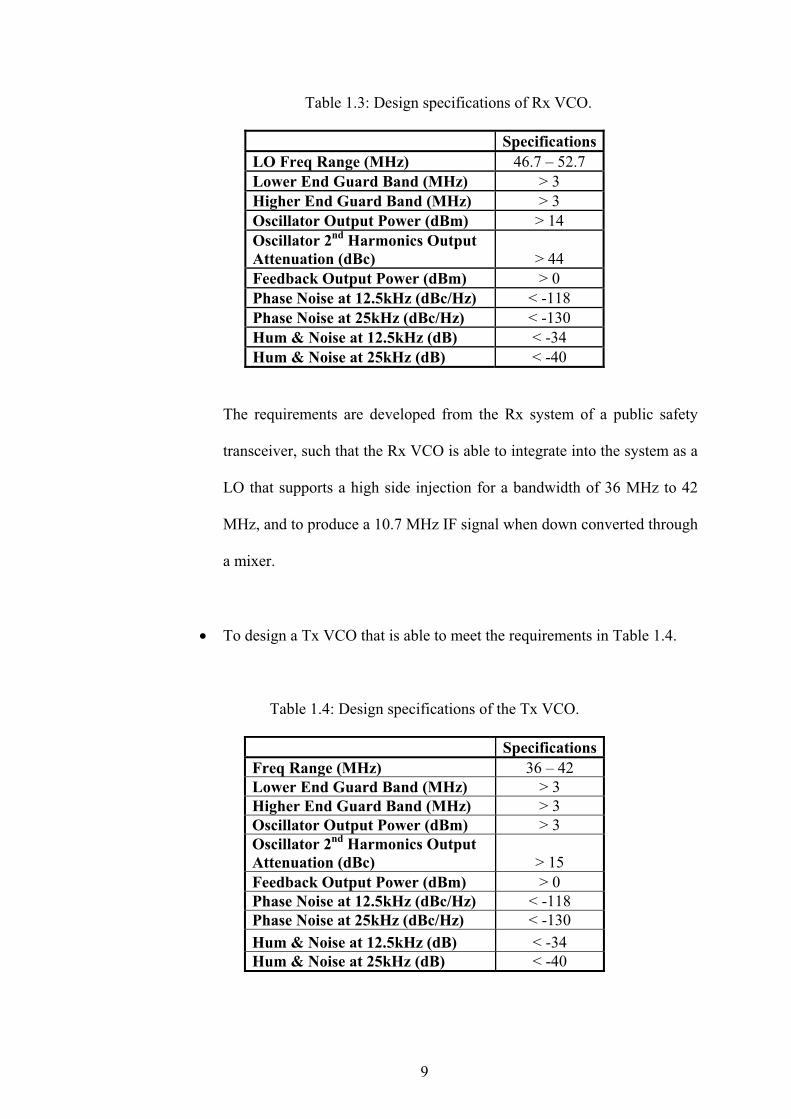
Table 1.3: Design specifications of Rx VCO.
Specifications LO Freq Range (MHz) 46.7 – 52.7 Lower End Guard Band (MHz) > 3 Higher End Guard Band (MHz) > 3 Oscillator Output Power (dBm) > 14 Oscillator 2nd Harmonics Output Attenuation (dBc) > 44 Feedback Output Power (dBm) > 0 Phase Noise at 12.5kHz (dBc/Hz) < -118 Phase Noise at 25kHz (dBc/Hz) < -130 Hum & Noise at 12.5kHz (dB) < -34 Hum & Noise at 25kHz (dB) < -40
The requirements are developed from the Rx system of a public safety
transceiver, such that the Rx VCO is able to integrate into the system as a
LO that supports a high side injection for a bandwidth of 36 MHz to 42
MHz, and to produce a 10.7 MHz IF signal when down converted through
a mixer.
� To design a Tx VCO that is able to meet the requirements in Table 1.4.
Table 1.4: Design specifications of the Tx VCO.
Specifications Freq Range (MHz) 36 – 42 Lower End Guard Band (MHz) > 3 Higher End Guard Band (MHz) > 3 Oscillator Output Power (dBm) > 3 Oscillator 2nd Harmonics Output Attenuation (dBc) > 15 Feedback Output Power (dBm) > 0 Phase Noise at 12.5kHz (dBc/Hz) < -118 Phase Noise at 25kHz (dBc/Hz) < -130 Hum & Noise at 12.5kHz (dB) < -34 Hum & Noise at 25kHz (dB) < -40
9
The requirements are developed from the Tx system of a public safety
transceiver, such that the Tx VCO is able to integrate into the system as a
modulating source in which the signal is injected into the power amplifier
(PA).
1.7 Research Scopes and Limitations
The research scopes and limitations are outlined as follows:
� To design the VCO oscillator, through theoretical calculation.
� To design the VCO oscillator, with ADS Scattering Parameter (S-
parameter) and Harmonic Balance (HB) simulation, using different
component models: lump component model, RF component model, and
Momentum co-simulation model.
� To design the VCO buffer and pad attenuator, with ADS Large Signal S-
parameter (LSSP) simulation, using different component models: RF
component model and Momentum co-simulation model.
� To implement and evaluate the VCO buffer and pad attenuator. The co-
relativity of the simulated results to the actual measured results is
analyzed.
� To design the Rx pre-mixer low pass filter, through theoretical calculation.
� To design the Rx pre-mixer low pass filter, with ADS LSSP simulation,
using different component models: lump component model, RF
component model, and Momentum co-simulation model.
� To implement and evaluate Rx pre-mixer low pass filter. The co-relativity
of the simulated results to the actual measured results is analyzed.
10

� To design and implement the Rx VCO. The co-relativity of the simulated
results to the actual measured results is analyzed.
� To design and implement the Tx VCO. The co-relativity of the simulated
results to the actual measured results is analyzed.
� The research only focuses on the phase noise improvement of the VCO.
� The bandwidth of the VCO is limited to 6 MHz according to the operating
bandwidth in the low band range required for a public safety transceiver
unit.
� Other limitations encountered in this research include the Printed Circuit
Board (PCB) fabrication technology, the components placed, as well as
the equipments applied for evaluation.
1.8 Research Contribution
Using the low-phase-noise design technique, which is detailed in Chapter 3,
both the Rx and Tx VCOs designed in this research are able to generate RF signals of
remarkably low phase noise level, in which, when incorporated into a transceiver
system, would be able to comply with the FCC specifications. Thereby, the major
contribution of this research is to support two-way communication systems and base
stations, used in the public safety pool in the US, as well as other countries adopting
such specifications. Despite this, other contributions of this research are as follows:
� By disabling the Tx VCO, the design could operate as a single Rx VCO,
and vice versa. Single way communications applying only either VCO
include broadcast systems, radar systems, missile illuminators etc.
� Unlike S-parameter simulation, co-relativity for HB simulation has long
been an issue. Noises in VCO as well as parts parasitic are highly
11
unpredictable. This research provides an improved simulation method in
predicting the performance of a VCO design. This, in turn, contributes to
cycle time and cost reduction for the design.
� The VCO buffer and attenuator designs could be used as reference for
oscillator as well as RF amplifier designs of other frequency bands.
1.9 Thesis Organization
This thesis is organized into six chapters to cover the entire research work
and the theory related to the design. In chapter 2, literature review is detailed. This
chapter documents the theory of noise in VCO, the development of various phase
noise models, as well as methods in phase noise reduction.
Chapter 3 explains the methodology of the research. This includes the
derivation of the mathematical model for the common gate Field Effect Transistor
(FET) Colpitts oscillator, the overview of ADS simulation, and selection of
components. The test methodology in evaluating the prototype is also detailed.
Chapter 4 describes the design and simulation of the VCO, which covers the
oscillator circuitry, the buffer and pad attenuator circuitries, as well as the Rx pre-
mixer low pass filter circuitry.
Chapter 5 reports the measured results of the hardware and further compares
and discusses the data with the simulated results. The phase noise performance of the
design is further analyzed and detailed in this chapter.
Finally, in chapter 6, the overall performance and findings of the research is
concluded. Future work is recommended for further improvement of the design.
12

CHAPTER 2
LITERATURE SURVEY
2.0 Introduction
Resonance signal generated by oscillators suffer from fluctuations in both
amplitude and phase. Such fluctuations are caused by internal noise generated by the
components as well as external interference. Fluctuation in amplitude tends to be
suppressed by the nonlinear characteristics of the oscillator; however, phase
fluctuation is accumulated over a period of time. Phase fluctuation, also referred to as
phase noise, has hence, been the key interest to researchers. Several models have
been developed to formulate a more accurate phase noise performance and shall be
detailed in this chapter. The characteristics of phase noise as well as other noises
affecting the oscillator, with methods in noise reduction are also well elaborated.
2.1 Noise
The major source of noise in an oscillator is the active device, usually the
transistor. The noise sources in any oscillator circuit ultimately combine to form
amplitude modulation (AM) noise and phase modulation (PM) noise. The AM noise
component is usually ignored because the gain limiting effects of the circuit control
the output amplitude, allowing little variation due to noise. The PM noise is of great
concern because its magnitude is typically greater than the AM noise contribution
and directly affects the frequency stability of the oscillator (Siweris and Schiek, 1985)
and related noise sidebands.
The designer has limited control over the noise sources in a transistor. For
example, the bulk resistance of a transistor, upon which thermal noise depends on, is
13

an unchangeable, intrinsic property of the device. However, using knowledge on how
noise affects oscillator waveforms, the designer is able to substantially improve
phase-noise performance by the selection of bias point and signal level. The main
mechanisms for noise in a semiconductor device include both thermal fluctuations in
minority carrier flow as well as bulk and depletion area generation-combination
events (Buckingham, 1983). The effects of these processes are categorized as thermal
noise, shot noise, partition noise, burst noise, and flicker noise.
2.1.1 Thermal Noise
At any temperature above absolute zero, thermal agitation causes electrons in
any conductor or semiconductor to be moving at random. At any one instant of time,
the electrons may be concentrated in some areas more than others. These
concentrations produce thermal noise. Thermal noise is generated by the random
thermal motion of the electrons and is unaffected by Direct Current (DC), since
typical electron drift velocities in a conductor are much less than thermal electron
velocities. In a resistor R, thermal noise can be represented by a series voltage with
the spectral density of
kTR4f
V 2
��
, (2.1)
where k is the Boltzmann’s constant, T is the absolute temperature in 0K, and f� is
the bandwidth (Manasse, Ekiss and Gray, 1967). Thermal noise is present in any
linear passive device. In bipolar devices, the parasitic resistors can generate the
thermal noise. For Metal Oxide Semiconductor Field Effect Transistors (MOSFETs),
14

the resistance of the channel also generates thermal noise with the spectral density
given by
m
2
gkT4
32
fV
���
, (2.2)
where gm is the conductance of the channel (Razavi, 2001).
2.1.2 Shot Noise
Shot noise is associated with a DC and is presented majorly in diodes and
transistors. It is the fluctuation of the DC and is usually modeled as a noise current
source with the spectral density of
qI2f
I 2
��
, (2.3)
where q is the charge of an electron, I is the DC, and �f is the bandwidth
(Spangenburg, 1957).
In transistors, each current path will have its own associated shot noise. For
example, a Bipolar Junction Transistor (BJT) has shot noise for each of the emitter,
base, and collector currents (Thornton, 1966). An additional source of noise resulting
from shot noise is called partition noise. Partition noise occurs at current junctions
and is caused by each electron in making a decision to go one way or another. A
statistical fluctuation in the collector and base currents equating to noise occurs
(Krauss, Bostian and Raab, 1980). In a BJT, the majority of electrons flow from the
emitter into the collector. A fraction of the emitter current must also flow to the base.
15
The splitting of the emitter current into the base and collector current components
provides this basic partition noise contribution.
2.1.3 Flicker Noise
Flicker noise is found in all active devices as well as in some discrete passive
elements. It is not a broadband phenomenon like thermal and shot noise; in fact, it is
mainly caused by traps associated with contamination and crystal defects. The flicker
noise is also called as noise because it displays a spectral density of the form f/1
b
a
1
2
fIK
fI
��
, (2.4)
where I is the DC, , a, and b, are constants. The nonlinear performance of
oscillators transforms this low frequency by up-conversions into the near-
sidebands of the fundamental oscillation signal. The spectrum of noise varies
inversely with frequency and thus is only noticeable at low frequencies and near
sidebands. The low frequency performance is shown in Fig. 2.1. The upper
frequency at which the noise sinks into the noise floor caused by thermal and
shot noise is called corner frequency. This corner frequency is typically
between 100 Hz to 1 MHz and the low frequency limit of noise has been
followed to 10-7 Hz.
1K
f/1
f/1
f/1
f/1
f/1
A contributor to in a device is called Random Telegraph Noise (RTN),
also known as burst noise. RTN is the observed phenomenon whereby device current
switches between several discrete values at random times. RTN is closely linked with
noise in that it has spectral components which contribute to low frequency
f/1
f/1
16

noise (Kogan, 1966). A plot showing the RTN noise characteristics is shown in Fig.
2.2.
Figure 2.1: Spectral density of flicker noise versus (vs.) frequency
Figure 2.2: General RTN characteristic
2.2 Phase Noise
The signal shown in Fig. 2.3 is an ideal oscillating signal produced by an
ideal oscillator, in which the signal as a function of time is
, (2.5) ( ) [ t�cosVtV ��out = ]
where is the nominal amplitude and V is the nominal frequency at time t. In
frequency domain, this signal is presented by a single spectral line. However, in
17
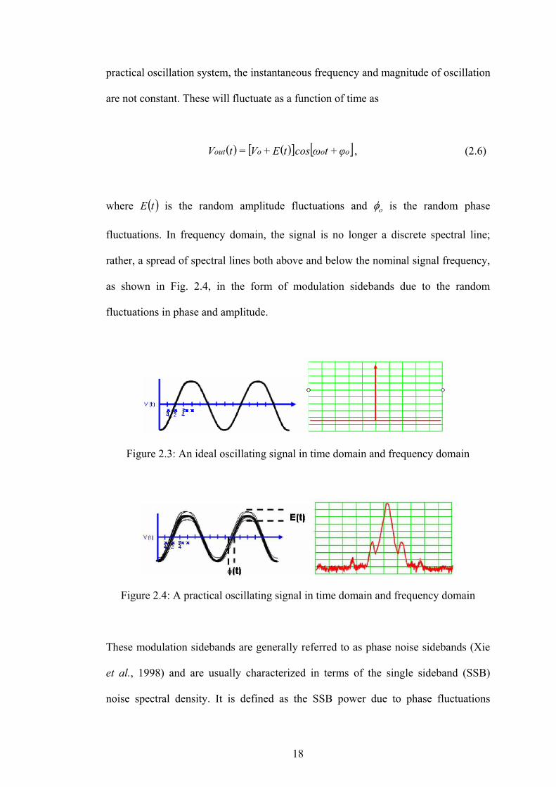
practical oscillation system, the instantaneous frequency and magnitude of oscillation
are not constant. These will fluctuate as a function of time as
( ) ( )[ ] [ ]���out �t�costEVtV ++= , (2.6)
where is the random amplitude fluctuations and � �tE � is the random phase
fluctuations. In frequency domain, the signal is no longer a discrete spectral line;
rather, a spread of spectral lines both above and below the nominal signal frequency,
as shown in Fig. 2.4, in the form of modulation sidebands due to the random
fluctuations in phase and amplitude.
Figure 2.3: An ideal oscillating signal in time domain and frequency domain
Figure 2.4: A practical oscillating signal in time domain and frequency domain
These modulation sidebands are generally referred to as phase noise sidebands (Xie
et al., 1998) and are usually characterized in terms of the single sideband (SSB)
noise spectral density. It is defined as the SSB power due to phase fluctuations
18

referenced to the carrier frequency power in 1 Hz bandwidth at a specific offset
frequency from the carrier divided by the signal’s total power, with unit dBc/Hz:
� � ���
���
� ���
carrier
sideband
PHz1,Plog10L �� , (2.7)
where � �Hz1,Psideband � � represents the SSB power at a frequency offset of
� from the carrier with a measurement bandwidth of 1 Hz as visualized in Fig. 2.5,
and is the power of the carrier signal. carrierP
Figure 2.5: Phase noise referenced to the carrier frequency power in 1 Hz bandwidth
The advantage of this parameter is its ease of measurement. Its disadvantage
is that it shows the sum of both amplitude and phase variations. However, it is
important to understand the amplitude and phase noise separately because they
behave differently in the circuitry. For instance, the effect of amplitude noise is
reduced by the intrinsic amplitude limiting mechanism in oscillators and can be
practically eliminated by the application of a limiter to the output signal, while the
phase noise cannot be reduced in the same manner.
The destructive effect of phase noise can be significantly seen in the front-
end of a super-heterodyne transceiver. Recapitulating the transceiver block diagram
19

in Fig. 1.1, the LO that provides the carrier signal for both mixers is embedded in a
frequency synthesizer. If the LO is noisy, both the down-converted and up-converted
signals are corrupted. As shown in Fig. 2.6, a large interferer in an adjacent channel
may accompany the wanted signal. When two signals are mixed with the LO output
exhibiting phase noise, the down-converted band consists of two overlapping spectra,
with the wanted signal suffering from significant noise due to the tail of the interferer
signal. This effect is referred to as “reciprocal mixing” (Krafcsik and Dawson, 1986).
Therefore the output spectrum of a LO has to be extremely sharp. Such stringent
requirements impose a great challenge in low-noise oscillator design.
Figure 2.6: Effect of phase noise onto the wanted signal
Over the years, several phase noise models have been studied and developed
to predict the phase noise performance of the oscillator and, thus, in pursuance of
further improvement. Some of the commonly used models are detailed in the
following sub-sections.
2.2.1 Leeson’s Model
D. B. Leeson proposed an empirical phase noise model to describe the phase
noise depicted in Fig. 2.7. Noise prediction using Leeson’s model (1966) is based on
20

the time-invariant properties of the oscillator such as the resonator Quality (Q),
feedback gain, output power, and noise figure. According to this model, the phase
noise generated by an oscillator can be expressed as:
� ��
���
��
���
���
�
���
���
���
�
���
����
���
!����
�
�
�� 3f/1
2
LS
1Q2
1PFkT2log10L , (2.8)
where � �L is SSB noise spectra density in units of dBc/Hz. The symbol k is the
Boltzmann’s constant, T is the absolute temperature in 0K, is the carrier power, SP
is the oscillation frequency, and � is the offset frequency from . is the
loaded Q of the oscillator resonator, F is the noise figure of the oscillator, and
LQ
3f/1� is the corner frequency between and region.2f/1 3f/1
As shown in Fig. 2.7, the general phase noise output spectrum of an oscillator
consists of 3 distinct sections allocated in the sideband. Immediately surrounding the
carrier frequency there exists a region of noise which decay as . At some
frequency offset called the – corner frequency, the noise spectrum
changes to a dependence. The region continues on to the phase noise
floor of the circuit. The noise floor of the circuit is a result of thermal and shot noise
sources. The noise floor exists across all frequencies, even in the and
region. The relative power associated with each section depends on each section’s
corner frequency and the noise floor level. The region is unavoidable as it is a
result of the characteristics of the resonator. Any Inductor-Capacitor (LC) resonator
will have a voltage dependence which varies as from the center frequency.
Since power is proportional to voltage squared, the resulting power spectrum is
3f/1
3f/1 2f/1
2f/1 2f/1
2f/1 3f/1
2f/1
f/1
21

therefore . The region comes from up-converted noise of the
device. The dependency appears when is multiplied by the
characteristic of the resonator.
2f/1 3f/1 f/1
3f/1 f/1 2f/1
Figure 2.7: SSB oscillator phase noise output spectrum
In Leeson’s model, 3f/1� is equal to the noise corner frequency of the
device. In practice, however,
f/1
3f/1� is rarely equal to the noise corner
frequency of the device. An existing problem is that the noise figure of an oscillator
is extremely difficult to predict (Robins, 1982). The factor F remains a co-relation
factor which can only be determined by measurement of the phase noise spectrum of
the oscillator. Since F and
f/1
3f/1� must almost always be measured from the
oscillator spectrum, the predictive power of Equation 2.8 is quite limited. From
Equation 2.8, it can be seen that the corner frequency at which the sinks into
the noise floor is exactly equal to the resonator half bandwidth,
2f/1
Q2/ . This also is
not completely justifiable.
In short, according to Leeson’s model, the only way to improve � �L is to
increase the output power or increase the loaded Q of the resonator. The oscillator
22

must be designed in such a way that the transistor does not saturate. Saturation
lowers the Q of the entire oscillator circuit, thus increasing phase noise and
harmonics level (Rhea, 1990).
2.2.2 Linear Time Invariant (LTI) Model
It is convenient to model an LC cross-coupled oscillator as a one-port
negative resistance model as shown in Fig. 2.8. In this model, the transconductance
of the active circuit, , must compensate for the loss caused by the parasitic
resistance, , in the tank, which is simply modeled as a parallel resistor.
mG
pR
Figure 2.8: One-port negative resistance oscillator with noise current in the tank
The thermal noise it generates, is modeled as a noise current, 2ni , parallel with
the tank. The thermal noise introduces the phase noise at the output of the oscillator.
The transfer function from the noise current to the output voltage in closed-loop
operations is derived as
� � � �2
2pm
2n
2n2
R,noise LCsR/1GsL1sL
iVsT
p ���
�
���
�
����� , (2.9)
23
where � �sT 2R,noise p
is the transfer function of the phase noise of the oscillator and 2nV
is the output voltage. With pm R/1G � , it can be shown that the transfer function at
small offset frequency, � , is approximated as (Craninckx and Steyaert, 1995).
� �2
2R,noise C
Lj2
1Tp �
�
���
����
�� , (2.10)
where is the equivalent impedance of the tank at the frequency 2R,noise p
T � " .
Accordingly, the one-side spectral density of the output noise voltage is
� � � 22p
2g,on L
2kTg4V
p �
� ����
� !�� �
�
, (2.11)
where � �2g,on p
V is the output noise voltage at offset frequency � and is the
conductance, that is . The noise voltage described here actually includes
both the amplitude noise (AM noise) and the phase noise (PM noise). If the oscillator
employs an Automatic Gain Control (AGC) circuit, the AM noise will be removed
for frequency offset less than the AGC bandwidth. In addition, the nonlinearity of the
oscillator determines oscillation amplitude and it can be viewed as an internal AGC
mechanism in oscillators. Therefore, even when there is AM noise, it will decay
away with time and thus has little effect on output phase noise. Neglecting the AM
noise results in a 0.5 factor multiplied to Equation 2.11. So, the spectral density of
the noise voltage is
pg
pp R/1g �
24