DESIGN OF HIGH EFFICIENCY HLE - NASA · charge-induced (OCI) HLE cell, and (b) a new HLE cell...
14
DESIGN OF HIGH EFFICIENCY HLE SOLAR CELLS A. Neugroschel and F. A. Lindholm Department of Electrical Engineering University of Florida SUMMARY A first-order analysis of HLE cells is presented for both beginning-of-life (BOL) and end-of-life (EOL) conditions. Based on this analysis and on experi- mentally observed values for material parameters, we present design approaches for both space and terrestrial cells. The approaches result in specification of doping levels, junction depths and surface conditions. The proposed struc- tures are projected to have both high VOC and high JSC, and consequently high T-I. 1. INTRODUCTION The purpose of this paper i s to discuss design approaches for silicon HLE solar cells. Design of cells for radiation and terrestrial environments are considered. Two main types of HLE cells receive attention: (a) the oxide- charge-induced (OCI) HLE cell, and (b) a new HLE cell having a wide p-epi taxial emitter for which the appropriate choices of emitter width and doping levels in the emitter and base are made to yield both high V and high JSC. OC SYMBOLS 2 Da ambipolar diffusivi ty (cm /sec) 2 Dn' Dp electron and hole diffusivi ties (cm /sec) 2 0 oxide charge density (C/cm ) 2 Js~ short circuit current density (A/cm ) 2 Jn~, J p ~ dark electron and hole saturation current density (A/cm ) Ln' Lp electron and hole diffusion length (cm) An ,AP excess electron and hole concentration ( ~ m - ~ ) h his work was supported by NASA Grant NSG-3018. https://ntrs.nasa.gov/search.jsp?R=19790024476 2019-02-02T22:03:35+00:00Z
Transcript of DESIGN OF HIGH EFFICIENCY HLE - NASA · charge-induced (OCI) HLE cell, and (b) a new HLE cell...

DESIGN OF HIGH EFFICIENCY HLE SOLAR CELLS
A. Neugroschel and F. A. Lindholm Department of Elect r ical Engineering
University of Florida
SUMMARY
A f i r s t - o rde r analysis of HLE c e l l s i s presented f o r both beginning-of-life
( B O L ) and end-of-l ife ( E O L ) conditions. Based on t h i s analysis and on experi-
mentally observed values f o r material parameters, we present design approaches
f o r b o t h space and t e r r e s t r i a l c e l l s . The approaches r e s u l t in specif icat ion
of doping leve l s , junction depths and surface conditions. The proposed s t ruc-
tures a r e projected t o have both high VOC and high JSC, and consequently high T-I.
1 . INTRODUCTION
The purpose of t h i s paper i s t o discuss design approaches f o r s i l i con HLE
so la r c e l l s . Design of c e l l s f o r radiat ion and t e r r e s t r i a l environments a r e
considered. Two main types of HLE c e l l s receive a t t en t ion : ( a ) the oxide-
charge-induced (OCI) HLE c e l l , and (b ) a new H L E c e l l having a wide p-epi taxia l
emit ter f o r which the appropriate choices of emit ter width and doping leve l s i n
the emit ter and base a re made t o y ie ld both high V and high JSC. OC
SYMBOLS
2 Da ambipolar d i f fus iv i t y (cm /sec)
2 Dn' Dp electron and hole d i f fus iv i t i e s (cm /sec)
2 0 oxide charge density (C/cm )
2 J s ~ shor t c i r c u i t current density (A/cm )
2 J n ~ , J p ~ dark electron and hole sa turat ion current density (A/cm )
Ln ' L p electron and hole diffusion length (cm)
A n ,AP excess electron and hole concentration ( ~ m - ~ )
h his work was supported by NASA Grant NSG-3018.
https://ntrs.nasa.gov/search.jsp?R=19790024476 2019-02-02T22:03:35+00:00Z

i n t r in s i c ca r r i e r concentration
BOL
EOL
E , B
electron and hole surface concentration (cm-')
oxide charge dependent electron surface concentration
( ) -I-
donor concentration in n and n material ( ~ m ' ~ ) + acceptor concentration in p and p material ( ~ m ' ~ )
electronic charge (Coulombs)
hole surface recombination velocity (cm/sec)
effect ive surface recombination velocity (cm/sec)
temperature ( O C , O K )
appl ied voltage (Volts)
open c i r cu i t voltage (Volts)
open c i r cu i t voltage established by base and emitter
(Volts)
emitter thickness (cm)
junction depth (cm)
r e s i s t iv i ty (R cm)
1 ifetime of minori ty electrons and holes (sec) +
associated with p and p region +
associated with n and n region beginning-of-life
end-of-1 i f e
associated with emitter and base
11. OCI-HLE CELL
Fig. 1 ( a ) shows the cross-section of an OCI s i l icon HLE solar ce l l . The principles of operation of th i s c e l l , which have previously been discussed [ I ]
are i l lus t ra ted in Figs. 1 ( a ) and 1 ( b ) . A positive charge Q O y achieved by su i t -
able heat treatment [2,31, induces an electron accumulation and an e l ec t r i c f i e ld near the s i 1 icon surface which reduces the effect ive surface recombination
velocity fo r holes Seff t o [4]
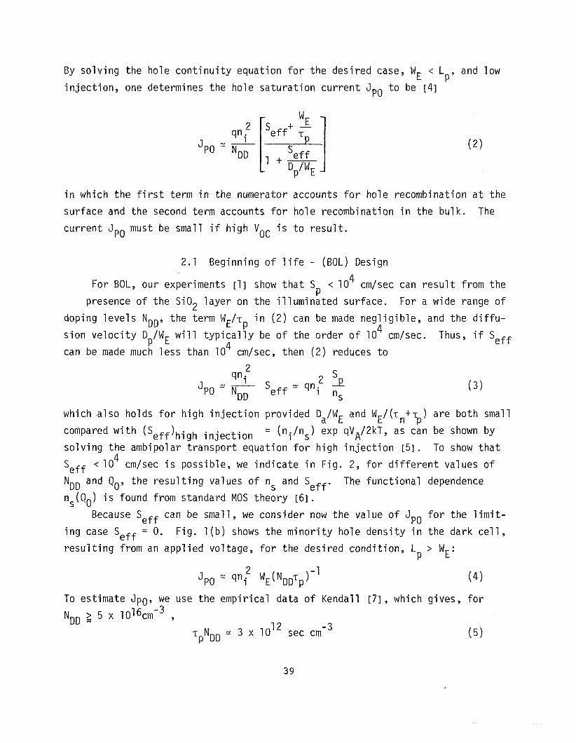
By so l v ing the hole c o n t i n u i t y equat ion f o r t he des i red case, WE < L and low P '
i n j e c t i o n , one determines the ho le s a t u r a t i o n c u r r e n t Jpo t o be [4]
i n which the f i r s t term i n the numerator accounts f o r hole recombinat ion a t the
sur face and the second term accounts f o r ho le recombinat ion i n the bu lk . The
cu r ren t Jpo must be smal l i f h igh VOC i s t o r e s u l t .
2.1 Beginning o f l i f e - (BOL) Design
4 For BOL, our experiments [I] show t h a t SD < 10 cm/sec can r e s u l t f rom the
presence o f the Si02 l a y e r on the ill umineted surface. For a wide range o f
doping l e v e l s NDD, the term W /T i n ( 2 ) can be made n e g l i g i b l e , and the d i f f u - E P 4
s ion v e l o c i t y D / W w i l l t y p i c a l l y be o f the order o f 10 cm/sec. Thus, i f Sef f P E n
can be made much l e s s than 10- cm/sec, then (2 ) reduces t o
which a l so holds f o r h igh i n j e c t i o n prov ided Da/WE and WE/(^ + T ) a re both small n P
compared with (Sef f )high injection = (ni/ns) exp qVA/2kT, as can be shown by
so l v ing the ambipolar t ranspor t equat ion f o r h igh i n j e c t i o n [5 ] . To show t h a t 4
' e f f < 10 cm/sec i s poss ib le , we i n d i c a t e i n Fig. 2, f o r d i f f e r e n t values o f
NDD and QO, t he r e s u l t i n g values o f n and Sef f . The func t i ona l dependence S
ns(QO) i s found from standard MOS theory [6] . Because Sef f can be smal l , we consider now the value o f Jpo f o r the 1 i m i t -
i n g case Sef f = 0. F ig. 1 (b ) shows t h e m i n o r i t y ho le dens i t y i n the dark c e l l ,
r e s u l t i n g from an app l i ed voltage, f o r the des i red cond i t ion , L > WE: P
wE ( N ~ ~ T ~ 1-' Jpo = (Ini ( 4 )
To est imate Jpo, we use the empi r ica l data o f Kendall [ 7 ] , which gives, f o r
2 5 x 1016cm-~ , N~~ - r N = 3 x 10" sec cm-3
P DD ( 5 )

JpO = 7 x 10' 12 E (6)
2 Thus, i f JSC = 35 mA/cm ( A M O ) , which was seen in OCI-HLE ce l l s , the open-circuit
voltage l imi t , ( V O C ) E = kT/q kn(JSC/JpO), established by the emitter current J PO
i s , for example, 800 mV, 780 m V , and 718 mV for W E = 2 pm, 5 um, and 50 um, respectively, independent of NDD (provided low-injection 1 eve1 s are maintained).
From a design viewpoint, t h i s demonstrates tha t ( V O C ) E > 700 mV can be achieved
for a wide variety of choices of NDD and W E provided only that L > W E . P
2.2 End-of-Life ( E O L ) Design
Radiation damage increase S and Q0 181 ; i t wi 11 a1 so reduce r [ 9 $1 01 . As P P
a design approach, we choose WE small compared with anticipated degraded diffu-
sion length to minimize bulk recombination; tha t i s , we require W E < L ( a f t e r P
i r radiat ion) . Then ( 2 ) s t i l l applies, and J i s determined by the velocities P 0
Seff , and D / W As a worst-case l imit , we consider the case Seff = a. P E*
Then the t r ans i t time tt for holes to cross the emitter i s
which, for example, i s of the order of 10-'sec for W E 2 pm. Thus , i f T a f t e r P
irradiation is larger than lo-' sec, the emitter will be transparent t o holes
and ( 2 ) reduces t o 3
This worst-case dependence suggests that NDD should be large enough, both
to assure small la teral ser ies resistance and to decrease JnO, b u t small enough
to avoid heavy-dopi ng degradation. For example, consider ardesi gn w i t h 18 -3
- 2 W E = 2 um, and NDD = 10 cm . For T = 2 5 ' ~ and JSC i; 25 mA/cm ,
2 ( V O ~ ) ~ > 640 mV. For electron f l uences up to 10' cm- , JSC = 25 mA/cm i s
2 expected i f prior t o radiation JSC = 35 mA/cm [lo] .
2.3 Examples of VOC established by the emitter for BOL and EOL
We have previously discussed ( V O C ) E for two 1 imiting cases: Seff = 0,
40

w h i c h corresponds t o the BOL condit ion, and Seff = m y which corresponds t o the
EOL condition. We now remove these l imit ing-case assumptions by considering
intermediate values of Seff , as determined by (1 ) and the condition t h a t 3 7 10 cm/sec < S < 10 cm/sec. The lower bound on S i s e a s i l y achieved, as i s
P P indicated by our experiments f o r a surface passivated by Si02 111. The upper
bound i s a theoret ica l l i m i t f o r a s i l i con surface [ I l l .
In Fig. 3 we p lo t ( V O C ) E a s a function of S fo r two values of emit ter P
widths W E = 2.5 um and 15 um and f o r emit ter doping dens i t i e s of N D D = 1017
and 1018 ~ m - ~ . Three values of oxide charqe dens i t i e s a r e considered: "
( a ) QO/q = 4 x 10" cm-', which i s the order of magnitude obtained in thermally
grown dry oxides followed by oxygen heat treatment a t about 700 C [2,3] before 12 -2 - 3 the i r r ad i a t i on ; and QO/q = 1 x 10 cm and 5 x lo-" cm , which i s the range
of values expected a f t e r i r rad ia t ion [8] . As shown i n Fig. 3 f o r BOL w i t h 3 S - 10 cm/sec, the emit ter recombination i s no ba r r i e r f o r achieving
P ( V O C ) E 2 700 mV f o r var ie ty of emit ter doping l eve l s and thicknesses. After
i r r ad i a t i on , f o r E O L , S i s expected t o increase s ign i f i can t ly [ 8 ] , b u t wil l not P 6
be l a rger than the order of 10 cm/sec [ I l l . B u t QO/q wil l a l so increase, as
mentioned above, which wil l increase nS [6] , and Seff = N D D S / n ( Q O ) wi l l depend on the r a t i o S / n (QO) a f t e r the i r r ad i a t i on . I t follows from Fig. 3,
P s consis tent w i t h our previous worst-case calcula t ion, t h a t ( V O C ) E > 650 mV i s
s t i l l possible a t EOL, i f W E < (Lp)EOL.
2.4 V O C established by the base f o r BOL and EOL
As shown in Fig. 1 ( b ) f o r the dark case with applied voltage V A y the quasi-
neutral sa tura t ion current J O in low in jec t ion , neglecting heavy-doping e f f ec t s
[12], i s J O = JpO + JnO, and the base sa tura t ion current i s
- 3 TO minimize J note t h a t , f o r N~~ cm , D , / N ~ ~ L , i s a decreasing n o '
function of NDD[13], provided heavy doping e f f ec t s a r e negl ig ible . As a r e s u l t ,
the open-circuit voltage l imited by the base (VOC)B i s an increasing function 19 -3 of N D D un t i l NAA - 10 cm (phase - 0.01 ~ c m ) which i s a doping level a t which
the heavy doping e f f ec t s i n p-type material become important ~ 1 2 1 , as shown i n
Fig. 4. The broken l ine in Fig. 4 shows an experimental dependence of VOC on
N~~ [14] which peaks a t N A A = 5 x 10¹⁷ ~ m - ~ . This i s a resu l t of the increasing
importance of the emitter current J for base dopings larger than about PO '
5 x m 3 , in conventional c e l l where the emitter current is not suppressed
by an HLE s t ructure such as tha t present in the proposed device.
3. Design concepts for space and t e r r e s t r i a l applications
Based on the foregoing analysis we present design concepts fo r two different
types of space ce l l s and f0 r . a t e r r e s t r i a l ce l l . +
1 ) 1 Fig. 5 shows a cel l designed fo r space applications. The p-type base dop-
ing i s N A A z 5 x 10' (p = 0.1 ~ c m ) which appears to be an optimum value which
gives Ln i n a range of 85-150 um in a finished cel l ~ 1 5 1 . This long diffusion
length, which will assure collection of most of the generated minority electrons,
provides a high value of the short c i r cu i t current JSC. The epitaxial emitter 17 i s narrow, about 2 ~ m , and highly doped, NDD 2 10 to 1018 c ~ n - ~ , to assure low
ser ies resistance. The thinness of the emitter of fse ts , t o a large degree, the
effects of significant degradation of l ifetime in the n-type material a f t e r the
i r radiat ion [ g ] . The H-L emitter junction can be achieved using e i ther OCI
induced or diffused n+ layer 1161.
The following conclusions about t h i s s t ructure can be made based on the
discussion in the previous sections:
a ) (VOC)E > 650 mV a t EOL, i f tt <
b ) ( V O C ) B a t EOL will depend on the radiation damage (101. Since the
base i s the same as in the conventional n on p c e l l , resu l t s obtained
f o r the conventional cel l radiation damage [lo] also apply here. -
c ) ( J S C ) ~ o L - (JSC)conventional + (JSCIE . base
S i n , where both S and nS increase d) For an OCI s t ructure, Seff = NDD P
with radiation, thus tending t o keep Seff low. Seff controls (JSC)E
and J PO ' 3
e ) For BOL, w i t h SD 2 10 cm/sec, (VOC)E > 700 mV, and (VOC)B depends on
minimizing Dn/L; N A A (VOC)B of the order of 700 mV can be expected fo r phase = 0.1 ncm with Ln > 75 pm.

f ) For Qo/q > 10" cm-', heavy doping e f f e c t s i n the accumulation l a y e r
may become important [Fig. 21. However, s ince the accumulation , .ayer
i s very narrow, these e f f e c t s a re expected t o be very small 1171.
g) A s t r u c t u r e w i t h a d i f f u s e d n+-region o f f e r s l a r g e r f l e x i b i l i t y i n +
choosing NDD because o f the low shunt ing res is tance o f the n - d i f f u s e d
1 ayer. + +
2) A wide-emi t t e r p -p-n space c e l l
We propose a new s i l i c o n s o l a r c e l l s t r u c t u r e [18] which i s p ro jec ted t o 2 have both h igh JSC(45 mA/cm ) and h igh VOC(700 mV) and consequently h igh q
(20%, AMO). The new s t r u c t u r e i s p ro jec ted t o have good performance i n rad ia -
t i o n as w e l l as non- rad ia t ion environments.
The s t r u c t u r e i s shown i n Fig. 6. The q u a l i t a t i v e sketches showing the
m i n o r i t y c a r r i e r d i s t r i b u t i o n s i n F ig. 1 a re v a l i d f o r t h i s case, too, w i t h
hole and e l ec t ron p r o f i 1 es reversed.
We emphasize some spec ia l fea tures o f t h i s s t r u c t u r e :
a ) The sur face i s passivated w i t h Si02 on top o f which a s u i t a b l e a n t i r e -
f l e c t i o n (AR) coa t i ng i s deposited. The H-L e m i t t e r j u n c t i o n i s +
achieved by a t h i n ( ~ 0 . 1 pm) p - d i f f u s e d l a y e r r e s u l t i n g i n [4]
+ where ( NAAIeff ' 1019 cm-3 i s the e f f e c t i v e doping i n t he p+-di f fused
l a y e r f o r ~i~ 2 l o z 0 a t the surface. An e l e c t r o n recombinat ion 3 v e l o c i t y a t t he Si -Si02 i n t e r f a c e on the order o f 10 o r l e s s can be
17 -3 e a s i l y achieved [I]. Therefore, f o r NAA = 5 x 10 cm , Seff i s o f
t he order o f 10 cm/sec o r l ess ; thus Seff ' 0 i s a reasonable approxi -
mat i on.
b ) AS a r e s u l t o f Seff ' 0, and the choice o f a 50 pm wide e m i t t e r region,
about 90% [I 91 o f a1 1 avai 1 ab le o p t i c a l l y generated m i n o r i t y e lec t rons
w i l l be co l l ec ted . Using a 5% l o s s AR coat ing and 4% metal coverage n
the p ro jec ted AM0 JSC = 45 m ~ / c m ~ . P-type ma te r ia l i s chosen as a
reg ion from which the JSC i s c o l l e c t e d due t o smal ler s e n s i t i v i t y t o
t he r a d i a t i o n than seen i n n-type ma te r ia l [9] . - .
C ) The doping l e v e l i n the nc-base i s opt imized t o be about 1018 ~ m - ~ ,
which i s t he onset l e v e l f o r heavy-doping e f f e c t s [171. The doping

l e v e l i n t he e m i t t e r (%5 x 10¹⁷ ~ m - ~ ) i s chosen t o min imize NAA~,, [131.
d ) Using pub l i shed data f o r l i f e t i m e s f o r ho les and e lec t rons [7,13], we
can c a l c u l a t e by use of Eqs. ( 2 ) and (9 ) , f o r s t r u c t u r e shown i n 2 F ig . 6, t h a t t h e s a t u r a t i o n c u r r e n t J0 2 7 x A/cm , imp ly ing
2 VOC = 700 mV f o r JSC = 45 mA/cm a t 25Oc, and imp ly ing Q - 20% AMO.
e ) S i g n i f i c a n t d i f f e rences e x i s t between t h i s new c e l l and a p rev ious l y +
proposed e p i t a x i a l p -p-n c e l l [20] ; these are discussed i n d e t a i l i n
Ref. 18. + +
f ) An a l t e r n a t i v e r e l a t e d s t r u c t u r e (p -p-n-n ) can be made, which employs +
an n-n low-high j u n c t i o n back -su r face - f i e l d base [4 ] . Th is s t r u c t u r e
w i l l have h ighe r JSC a t BOL due t o improved c o l l e c t i o n o f m i n o r i t y
holes from t h e n-region o f t h e base. +
3) n -n-p OCI-HLE t e r r e s t r i a l c e l l (F ig . 1 )
There a re two approaches t o min imize t h e base c u r r e n t i n t h i s c e l l , F iq. 7: . . - a ) Choose phase = 0.1 ncm (NAA = 5 x ~ m - ~ ) . I n t h i s case Ln ? 70 um
2 i s requ i red f o r (VOC)B = 700 m~ ( 2 5 ' ~ and JSC = 35 mA/cm ). Such values
f o r Ln can be achieved i n f i n i s h e d c e l l s us ing a low temperature fab-
r i c a t i o n process [13,15]. E p i t a x i a l growth o f t h e e m i t t e r and a h igh-
temperature o x i d a t i o n r e q u i r e d f o r low S 111 may decrease Ln below the P
70 pm; t h i s would r e s u l t i n (VOC)B < 700 mV. The l a r g e s t VoC seen
experimental l y f o r a c e l l with phase = 0.1 ncm i s 643 mV AMO, a t 25 '~. 19 -3
b) A second approach i s t o use a h i g h l y doped p-type (5 x 10¹⁸ - 10 cm ) base. Note t h a t f o r NAA = 5 x 10¹⁸ ~ m - ~ , f o r example, L = 2 pm i s n s u f f i c i e n t t o achieve (VOC)B o f 700 mV. Such values a r e expected even
a f t e r t h e high-temperature f a b r i c a t i o n steps. I n t h i s second approach,
WE = 50 um, s ince t h e base w i l l c o n t r i b u t e n e g l i g i b l y t o JSC. Such a
wide e m i t t e r i s requ i red t o c o l l e c t about 90% o f generated m i n o r i t y
holes. I n approach (a ) , WE can range from about 10 t o 50 pm. The
l a r g e s t VOC seen exper imenta l l y f o r a c e l l w i t h phase = 0.024 Qcm
(NAA = 2.5 x 10¹⁸ ~ m - ~ ) i s 647 mV AMO, a t 25'~.
c ) E m i t t e r doping can be chosen f rom range o f about 5 x 1016 cm'3 t o 17 -3 about 5 x 10 cm

CONCLUDING REMARKS
F i r s t order analysis of H L E solar c e l l s for BOL and EOL conditions i s
presented. Based on t h i s analysis and on experimentally measured material para-
meters, design concepts for both space and t e r r e s t r i a l ce l l s a re discussed. -I-
The proposed structures include: n -n-p OCI-HLE space c e l l , wide emitter + + +
p -p-n space c e l l , and n -n-p OCI-HLE te r re s t r i a l cell . All structures a re
projected to yield both high VOC and JSC.
REFERENCES
Neugroschel, A . , Lindholm, F. A . , Pao, S. C , and Fossum, J . G . , "Emitter Current Suppression i n a High-Low-Junction Emitter Solar Cell Using An Oxide-Charge-Induced Electron Accumulation Layer," Appl. Phys. Let ters , vol. 33, July 15, 1978, pp. 168-170.
Deal, B. E . , Sc lar , M . , Grove, A . S . , and Snow, E . H . , "Characterist ics of the surface-s ta te charge ( Q s s ) of thermally oxidized s i l i con , J . Electro- chem. Soc., vol. 114-, March 1967, pp. 266-274.
F u , H. S. and Sah, C. T . , "Theory and experiments on surface l / f noise", IEEE Trans. Electron Devices, vol. ED-19, Feb. 1972, 273-285.
Godlewski, M. P . , Baraona, C. R . , and Brandhorst, H . W . , "Low-high junction theory applied t o so la r c e l l s " , in Record of Tenth IEEE Photovoltaic Spec ia l i s t Conf., 1973.
Lindholm, F . A . , Fossum, J . G . , and Burgess, E . L . , "Application of the superposition pr inciple t o sol ar-cel 1 analysis" , I E E E Trans. Electron Devices, vol . ED-26, March 1979, pp. 165-1 71 .
Kingston, R. H . and Neustandter, S. F . , "Calculation of the space charge, e l e c t r i c f i e l d and f ree c a r r i e r concentration a t the surface of semi- conductors, J . Appl . Phys., vol . 26, June 1955, pp . 718-720.
Kendall, D . , Conf. Physics and Application of Lithium Diffused Si l icon, NASA-Goddard Space Fl i ght Center, Dec. 1969.
Zaininger, K. H . and Holmes-Siedle "A survey of radiat ion e f f ec t s i n metal- insul ator-semiconductor devices", RCA Rev. , vol . 28, 1967, pp. 208-241 .
Cooley, W . C. and Janda, R . J . , "Handbook of space-radiation e f f ec t s on solar-cel l power systems", NASA Report SP-3003, 1963.
Tada, H . Y . and Carter , J . R . , "Solar c e l l radiat ion handbook", JPL Publica- t ion 77-56, 1977.
Heasel 1 , E. L . , "Recombination beneath ohmic contacts and adjacent oxide covered regions", Solid-State Electron., vol. 22, Jan. 1979, pp. 89-93.
Dunbar. P . M. and Hauser. J . R . . "Theoretical e f f ec t s of surface diffused region 1 ifet ime models on s i l i con so l a r c e l l s " , Sol id-State Electron., vol . 20, August 1977, pp. 697-701 .
I l e s , P. A. and Soclof, S. I . , "Effect of impurity doping concentration on so l a r ce l l output, i n Record of Eleventh Photovoltaic Spec ia l i s t Conf., 1975, pp. 19-24.

14. Godlewski, M . P . , Brandhorst, H. W . , and Baraona, C. R . , "Effects of high doping leve l s on s i l i con so la r ce l l performance", i n Record of Eleventh Photovoltaic Spec ia l i s t s Conf., 1975, pp. 32-35.
15. Brandhorst, H . W . and Godlewski, M. P . , p r ivate communication.
16. Lindholm, F. A . , Neugroschel, A . , Pao, S. C . , Fossum, J . G . , Sah, C . T . , "Design Considerations fo r Si l icon HLE Solar Cells", in Record of Thirteenth IEEE Photovoltaic Spec ia l i s t s Conf., 1978, pp. 1300-1305.
17. Lanyon, H . P. D . and Tuft , R . A , "Bandgap narrowing i n heavily doped s i l i - con", IEDM Technical Digest, Dec. 1978, pp . 376-319.
18. Neugroschel, A. and Lindholm, F. A , , submitted fo r publication to IEEE Trans. Electron Devices.
19. Fossum, J . G . , "Computer-aided numerical analysis of s i l i con so la r c e l l s " , Sol i d-State Electron. , vol . 19, Apri 1 1976, pp. 269-277.
20. D'Aiello, R . V . , Robinson, P . H . , and Kressel, H . , "Epitaxial s i l i con so la r c e l l s " , Appl. Phys. Let ters , vol. 28, 15 Feb., 1976, pp. 231-234.


5d I I I I /03 /04 105 /a /o '
SP ~cm/ser 4 . 3 . Dependence Of @ch on Sp .
f i 4. fiPnj,en&/ aqd d&~,.t,rs/ depndence a j & 9' OM &se dopiny . &ex8 resu/d5 06tuhed or? 052-HLE e~% ~ / r 6 " 3 m r / f i r O . / - R B
M S / Y ~ & ~ Y ~ r ; d 6 4 7 m L ' f w 0.024JZcm h x e re- S/S X * i ~ y /mcq5Ure~ t?/ NASA LPW,~, Ot 25*~, #NO).