VHDL Implementation of 4-Bit Full Adder Using Reversible Logic Gates
Upload
truongphucCategory
view
224download
4
International Conference on Communication and Signal Processing, April 3-5, 2014, India
Design Of All Optical Reversible Logic Gates
Kuki Bordoloi, T. Theresal, Shanthi Prince
Abstract-Considering the benefits of Quantum and Optics, if
the logic gates in the quantum field and electronic structure are
implemented using optical elements, then it will be benefited
from advantages of Quantum and design, and these processing
circuits can be used in optical computing and quantum computing, genetic processes, and other useful nanotechnology
applications. Advantages of reversible logic systems and circuits
have drawn a significant interest in recent years as a promising
computing paradigm having application in low power CMOS,
quantum computing, nanotechnology, and optical computing. In
this study, we have introduced reversible optical Double
Feynman gate using optical Mach-Zehnder interferometer (MZI)
switches with new design. The proposed optical Double Feynman
gate will be optical logic gate and reversible. As the proposed
gate is a complete one, it can implement all the MZI-based
quantum circuits.
Index Terms- Feynman Gate , Mach-Zehnder interferometer
(MZI), Optical Double Feynman Gate, Reversible Logic.
I. INTRODUCTION
In conventional computers, the computation carrying out
is irreversible i.e. once logic block generates the output bits, the input bits are lost [1]. But it is not in the case of reversible logic circuits. The classical set of gates such as AND, OR and EXOR are not reversible as they are all mUltiple input single output logic gates. A gate is reversible if the gate's inputs and outputs have a one-to-one correspondence, i.e. there is a distinct output assignment for each distinct input [2]. Therefore, a reversible gate's inputs can be uniquely determined from its outputs. Reversible logic gates must have an equal number of inputs and outputs [3]. Then the output rows of the truth table of a reversible gate can be obtained by permutation of input rows.
Reversible logic circuits have emerged as a promising
technology in the field of information processing. Irreversible
hardware computation results in energy dissipation due to
Kuki Bordoloi is with Department of Electronics and Communication Engineering, SRM University, Kattankulathur - 603 203, Tamil Nadu, India (e-mail: [email protected]).
T.Theresal is a assistant professor in Department of Electronics and Communication Engineering, SRM University, Kattankulathur - 603203, Tamil Nadu, India (e-mail:[email protected]).
Shanthi Prince is a professor in Department of Electronics and Communication Engineering, SRM University, Kattankulathur - 603 203, Tamil Nadu, India (e-mail: [email protected]).
978-1-4799-3358-7/14/$3\.00 ©2014 IEEE
information loss. On the other hand, the reversible logic
circuits offer an alternative that allows computation with
arbitrary small energy dissipation. There is number of existing
reversible gates in literature like Fredkin, Feynman and
Toffoli gates etc [4]. Each of these gates is universal, i.e. any
logical reversible circuit can be implemented using these
gates.
All-optical logic for optical network is an exciting field of
research where we can expect much innovation. High
capacity, low cost communication systems are needed to keep
up with the increasing demand for the broad band
communications. Photon being the ultimate unit of
information with unmatched speed and with data package in a
signal of zero mass, the techniques of computing with light
may provide a way out of the limitations of computational
speed and complexity inherent in electronics computing.
Different optical logic gates have already been proposed to
perform irreversible logic function. But, reversible
computation in a system can be performed if the system is
composed of reversible gates.
The all optical implementation of reversible gates can be
designed based on semiconductor optical amplifier (SOA)
based Mach-Zehnder interferometer (MZI) due to its
significant advantages such as high speed, low power, fast
switching time and ease in fabrication. Semiconductor optical
amplifier (SOA) based Mach-Zehnder interferometer (MZI)
can play a significant role in this field of ultra-fast all-optical
signal processing. The interferometer employs bidirectional
couplers and semiconductor amplifier in one of its arms.
Interferometer acts as a very high speed switch since it does
not need any conversation from optical to electronic and vice
versa.
This paper is organized as follows. In section II, principle and operation of MZI based optical switch is discussed. In section III, all-optical circuit of Feynman gate is discussed. All-optical circuit of Fredkin gate is discussed in section IV . Simulation results using OptiSystem software confirming describe methods are also given in this paper. In section V, a new design of reversible optical Double Feynman gate is proposed. Finally, the conclusions are formulated.
II. SOA BASED MACH-ZEHNDER INTERFEROMETER (MZI) SWITCH
Mach-Zehnder Interferometer (MZI) Switch, as shown in
the Fig.l and Fig.2 is a very powerful optical device to realize
ultra-fast all optical switching [5]. In this switch a
semiconductor optical amplifier is inserted in each arm of
MZI. The incoming signal to be switched is split between the
+,IEEE Advancing Technology
for Humanity
1583

arms of the interferometer. The interferometer is balanced so
that, in the absence of a control signal, the incoming signal
emerges from one output port. The presence of a strong
control pulse changes the refractive index of the medium. A
change in the index adds a phase shift between the two arms
of the interferometer, so that the incoming signal is switched
over to another output port. This method of switching is based
on cross-phase modulation (XPM).
A.8(BarPort)
A.B(CrossPort)
Fig. 1. Semiconductor optical amplifier based Mach-Zehnder
interferometer.
Incoming Signal
-
Control Si gnal
M
z
Bar Port 1---- (u pper channel)
1---_ Cross Port (lower channel)
Fig. 2. Mach-Zehnder interferometer based all optical switch.
There two input ports A and B called as incoming signal
port and control signal port respectively and two output ports
called as bar port and cross port respectively in a MZI switch
[6]. We consider no light or absence of light as the logic value
O. When there is an incoming signal at port A and control
signal at port B then there is a light present at the output bar
port and there is no light at the output cross port. In the
absence of control signal at the input control port B and when
there is an incoming signal at input port A then the outputs of
MZI are switched and result in the presence of light at the
output cross port and no light at the bar port. In the absence of
incoming signal at the input port A there is no light at both the
output ports. The above behavior of MZI can be written as
Boolean functions having inputs to outputs mapping as (A,B)
to (X = AB ,Y = AB ), given in Table I.
Table T Truth Table of MZl based switch
Input Output Incoming Control Bar Port Cross Port Signal Signal
0 0 0 0
0 I 0 0
1 0 0 1
I I I 0
The simulation setup of MZI based switch using OptiSystem software is shown in Fig. 3. OptiSystem is a
comprehensive design suite that enables users to plan, test, and
simulate optical links in the transmission layer of modern optical networks [7].
.... � OptaI TIIII Dcft:.ulVIltOlbr
� OpacoITIlll DomaiI V-_13r_2
�:!: t::s:!,�Gnr'!«J 6iI�'OIOl
Fig. 3. Simulation Setup of MZI switch in OptiSystem.
The simulated results of MZI based switch using OptiSystem as obtained in the optical time domain visualizer is given in Fig. 4.
1. ,1-' _--'=_.=L-,--""-'--,--,
1 •
::�:oo,�-t w i "" " " '�
_�. �=���'-"_ :,:�. c � -x vI 1.1 rc_",_
Input (0011)
R- � �_ c2!-:::!>:r!:: .... �,':..rn=:'I.u.llze� 3
i ,;'-' -..""L"..�=------""'-"-----"''''t .
-�.--������� ." -x yT,'.'
Input (0101)
�o <GOp :.A • A v'j , ••
Output (0001)
A
Output (0010)
U""" � :.:��;=o . MI""''''' ' "_1.00,.,..,, •
u .... - � :..:r;::,'.::o . """",.u, . "-I'�-"" •
Fig. 4. Simulated inputs and outputs of MZI switch.
1584
III. MZI BASED FEYNMAN GATE Feynman gate is a 2x2 reversible gate having A and B as
input vector and X and Y as output vector, where X=A,
Y=AG;>B [8], given in Table II.
Table II Truth Table of Feynman Gate
Input Output A B X Y
0 0 0 0
0 I 0 I
I 0 I 1
1 1 1 0
The circuit of all- optical MZI based Feynman gate is
shown in Fig. 5. and the simulation setup Feynman gate using OptiSystem software is shown in Fig. 6.
f-----+x
B , M Z Y
(, B
B5·3 B5·2
Fig. 5. All-optical circuit of Feynman gate. BC: beam combiner, �: EDFA, BS: 50:50 beam splitter.
�---. �---
�---�, . �---�,
Fig. 6. Simulation Setup of Feynman gate.
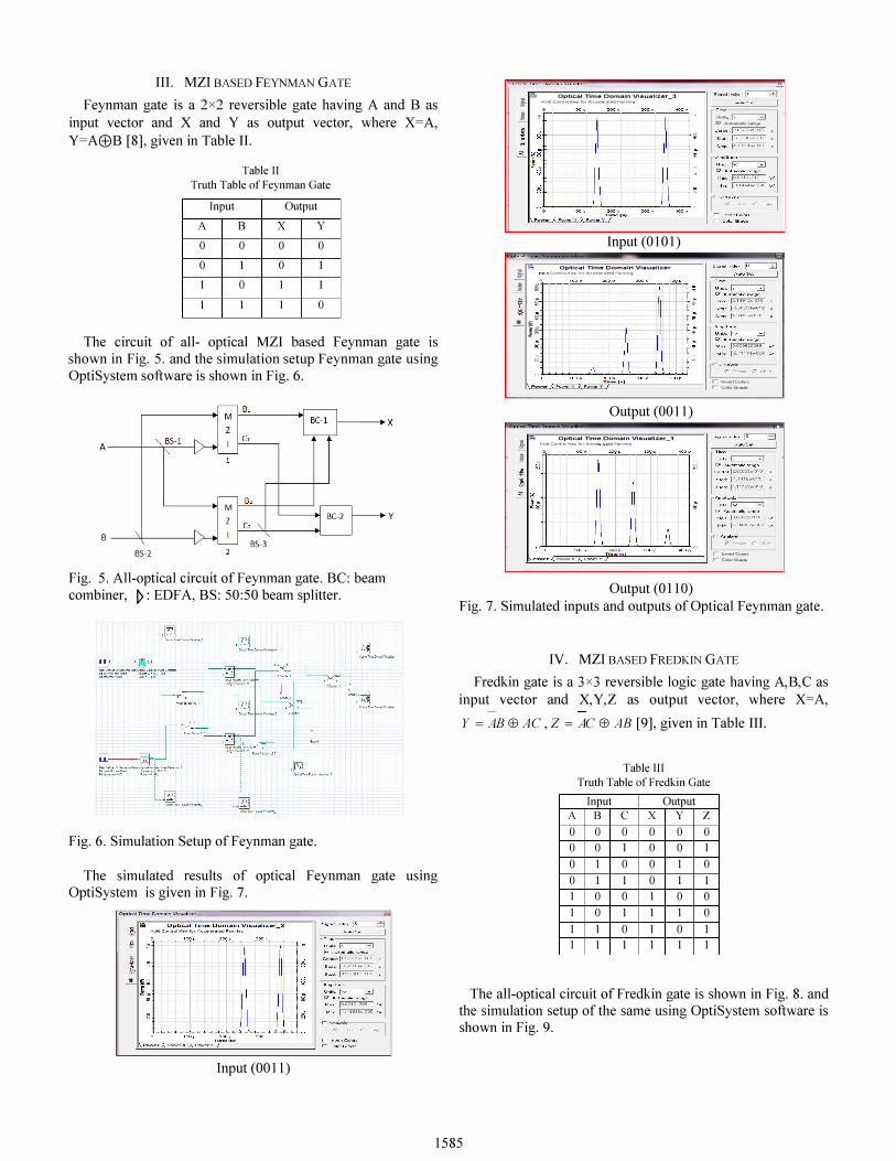
The simulated results of optical Feynman gate using OptiSystem is given in Fig. 7.
Input (0011)
� Optical Time Domain Vlsuallzer_3 . i <0. =.0" <� '''' Ao __ ,.,_ •••• A,
. � � 'it-' --""-"---="'-----"''-''---'''''-; ! §
��,---=-k���o-��� -"'�I\I'owoo<X �/!·t
Input (0101)
;,;. Optical TIme DOOleln Visualizer . i < 0. =.0" <� ,_ Ao ... ,,,_ •• MA,
L §' 1 � �
�� li!
Output (0011)
.. Optical Time Domain Vlsualizer_1
1- <O.��,"�''''A� .... _ •••• A,
L , ! �
�.
rA __ X A_v i Cal
Output (0110)
U� • ..----------:=: P Aut""'"""", ........ c_-i'���,,, • 5(...-,.1-679067".012 * "�I" "-'" .
r'n"."Coioo. rCoIooG,_
rlnve..Colo .. rCoIooG,_
Fig. 7. Simulated inputs and outputs of Optical Feynman gate.
IV. MZI BASED FREDKLN GATE Fredkin gate is a 3 x3 reversible logic gate having A,B,C as
input vector and X,Y,Z as output vector, where X=A,
Y = AB E9 A C ,Z = AC E9 AB [9], given in Table III.
Table III Truth Table of Fredkin Gate
Input Output A B C X Y Z
0 0 0 0 0 0
0 0 I 0 0 I
0 1 0 0 1 0
0 I I 0 I I
I 0 0 I 0 0
1 0 1 1 1 0
1 1 0 1 0 1
I I I I I I
The all-optical circuit of Fredkin gate is shown in Fig. 8. and the simulation setup of the same using OptiSystem software is shown in Fig. 9.
1585

A ____ �B�S�- l�--------------------------+X
B -----+-----+1
c ------+-----+1
M Z
M
i----+y
i---+Z
Optical Time Domain VisuaUzer_3 . � "_ <_._ '.' .� A_ •••• � '.ooA,
Z Output (00001111)
2
Fig. 8. All-optical circuit of Fredkin gate.
... �----.
=i?�--' �----.
Fig. 9. Simulation Setup of Fredkin gate.
The simulated results of optical Fredkin gate using OptiSystem is given in Fig. 10.
erA X A yT; •• ,
Input (00001111)
.1 H _c..?�t!�!<}!=..?:'�:n�r:;-'I.uanz • .- 2
.I! ! �
o
�,; 1:2"�j • ,; I :: :;;,::;::� : ...!.... £§" §
J. • 1 :::"�w1 � �
..... - 1",,3965.-006 wi -!!----��-=�:_____" _ I: :::_. r . '0 1
.. /\ "J\ yTj_ '.! r c"","o,_
Input (00110011)
.J. Ho .. �.!t!�! .... = .. ?'�";::nln';,;'I.uallz • .- 1
i !O.�-=�-=�-==--=�
! • •
,;
•
"
o�. � :_:'" .9'=0 . "_I�o�"" • "�Io"oo�"o •
O�"' � ':_Au<,=�= W M. I.�r_� w
-�o --�--������ "/I xX VI
(01010101)
Input
Optical Time Domain Vlauallz. .. r_4 � "_<_ ... _,_A __ .'�'.ooA,
� "
! � ...!.... £�
Hi
" ii • " "
: � A � l=:=������,-.1\ "J\P y T7 1.,
Output (00110101)
Output (01010011)
Fig. 10. Simulated inputs and outputs of Optical Fredkin gate.
V. PROPOSED MZI BASED ALL-OPTICAL DOUBLE FEYNMAN
GATE
Double Feynman gate is 3x3 reversible logic gate having A, B, C as input vector and X,Y,Z as output vector, where
X=A, Y=A(j;)B and Z=A(j;)C [10]. The schematic block diagram is shown in Fig. 11 and truth table is given in Table IV.
A{J:X
B DFG Y
C Z
Fig. 11. Schematic diagram of Double Feynman gate.
Table IV Truth Table of Double Feynman Gate
Input Output A B C X Y Z 0 0 0 0 0 0 0 0 1 0 0 1
0 I 0 0 I 0 0 I I 0 I I 1 0 0 1 1 1 I 0 I I I 0 1 I 0 1 0 1 I I I I 0 0
The all optical circuit of Double Feynman gate using
OptiSystem is shown in Fig. 12.
1586

(1) When A=B=C=O, i.e. when no inputs are given(absence
of light), then there is no output X=Y=Z=O.
(2) When A=B=O and C=I, incoming signal is absent at
MZI-l, MZI-2 and MZI-4,then no light comes out through
cross or bar port of MZI-l, MZI-2 and MZI-4. Incoming
signal is present at MZI-3 but control signal is absent. Hence,
the light beam emerging out through C3 gives the output
Z=1.Therefore, when A=B=O and C=1 then X=O, Y=O, Z=1. It
satisfies the second row of the truth table given in Table IV.
5-1 A X
65-3 Y
B 65-2
c -----''+--1>--+1
Fig. 12. All-optical circuit of Double Feynman gate. BC: beam
combiner, [> EDF A, BS: 50:50 beam splitter.
(3) When A=C=O and B=1 then incoming signal is absent at
MZI-2, MZI-3 and MZI-4. So no light comes out through
cross or bar port of MZI-2, MZI-3 and MZI-4.For MZI-l since
incoming signal B=1 and control signal A=O thus bar port
receives no light i.e. B,=O and cross port receives light so
C,=1 which gives the output Y=1. Therefore, when A=C=O
and B=1 then X=O, Y=I, z=o. It satisfies the third row of the
truth table given in Table IV.
(4) When A=O and B=C=I, then the MZI-2 and MZI-4
receives no light in the incoming port, so B2=C2=B4=C4=0.
MZI-l and MZI-3 receives the incoming signal and no control
signal thus B,=B3=0 and C,=C3=1 which gives x=o and
Y=Z=1. Therefore, when A=O and B=C=1 then X=O, Y=I,
Z=1. It satisfies the fourth row of the truth table given in Table
IV.
(5) When A=1 and B=C=O, then the MZI-l and MZI-3
receives no light in the incoming port, so B,=C,=B3=C3=0.
MZI-2 and MZI-4 receives the incoming signal and no control
signal thus B2=B4=0 and C2=C4=1, which gives X=Y=Z=1.
Therefore, when A=1 and B=C=O then X=Y=Z=1. It satisfies
the fifth row of the truth table given in Table IV.
(6) When A=C=1 and B=O, then the MZI-l receives no
light in the incoming port, so B,=C,=O. MZI-2, MZI-3 and
MZI-4 receives the incoming signal. But since B=O there is no
control signal in MZI-2 thus B2=0 and C2=1, which gives X=1
and Y=1. Both the MZI-3 and MZI-4 receives both the
incoming and the control signal thus B2=B4=1 and C2=C4=0,
which gives Z=O.Therefore, when A=1 and B=O and C=1 then
X=Y=1 and z=o. It satisfies the sixth row of the truth table
given in Table IV.
(7) When A=B=1 and C=O, then the MZI-3 receives no
light in the incoming port, so B3=C3=0. MZI-l, MZI-2 and
MZI-4 receives the incoming signal. Since c=o there is no
control signal in MZI-4 thus B4=0 and C4=1, which gives Z=1.
Both the MZI-l and MZI-2 receives both the incoming and the
control signal thus B,=B2=1 and C,=C2=0, which gives X=1
and Y=O.Therefore, when A=1 and B=1 and c=o then X=Z=1
and Y=o. It satisfies the seventh row of the truth table given in
Table IV.
(8) When A=B=C=I, then MZI-l, MZI-2, MZI-3 and MZI-
4 receives both the control and the incoming signal. Thus
B,=B2=B3=B4=1 and C,=C2=C3=C4=0, which gives X=I, Y=O
and z=o. Therefore, when A=1 and B=1 and C=1 then X=1
and Y=z=o. It satisfies the eight row of the truth table given in
Table IV.
The truth table for the proposed optical Double Feynman
gate is verified theoretically. The proposed model of optical
Double Feynman gate is being simulated using OptiSystem.
The simulation setup of the proposed optical Double
Feynman using OptiSystem software is shown in Fig. 13.
�.:;':!�-)� m:1 1Ioi_·Oll1ltOl
: . � C\a:.Or .. __ }
....... � OJ:o:oIr .. o......._
... )� Qr:oooI T ... ___ 1
Fig. 13. Simulation Setup of optical Double Feynman gate.
The simulated results of proposed optical Double Feynman
gate using OptiSystem is given in Fig. 14.
� Optical Tlrne Domain Viaualizer_2
..! K •• =."., O.y ,., A,_",.,_ ......
.� �o�_����_�_���
I �
��o--��--.=��.����� __ er !I. Poweo-" 1\ Power
y Tj I ••
Input (00001111)
Sjgn"llnde", �::t:l ,
r In"e"CQIo<� r CoIc<G,,,,d ...
1587

� Optical Time Domain Vi.uali�er_3
� I.." a"",,,n an« O" .. g.'" Se .. ct Zoom Rag"'n. Pr .... Cont<OI K .. y a n" I.a"
� �
�L-����. =�. __ -=��� _:0; _v
Input (00 1lO0 11)
!;;I Optical Time Domain Vi.uali�er_8
.� Co. ""'00 o� �o, <0 So.d ZOOm Ro,M �oo' =.,,", ••• .o" Co.
j " ,
Input (01010101)
;;, !;;I L ... au"o����':�!'�:ct��<:;=;� IO�:�=�:;'�:' K"Y " ncl L""
:l!
. =. <=r /I. X A P v
7 f.l
Output (00001111)
9 Optical TIme Domain Visuall:z.er_"
J- Co. ""," • • - �., ' .... d Zoom R., •• � ... =.,_, « .. _ c ••
. :!! i -� I �
Output (00111100)
� Optical Tlme Domain Vlsuall�er_5
. � Co. ""Ro • • � �., <0 So.d Zoom R.,". � ... =." ... oo .� Co.
A A .�"
.. r/l.....-.".xA_v/'·t
Output (OlOllOlO)
Sign"'llnde�: �:E)
r Inve,tCoIO<$ r CoIO<G".cie
Fig. 14. Simulated inputs and outputs of optical double
Feynman gate.
VI. CONCLUSION
In this paper, the all-optical design of reversible Double
Feynman gate is proposed and described. The simulation of
existing all-optical Feynman and Fredkin gates using
OptiSystem software are also done. All these gates can be
considered as basic gates and the arithmetic and logic
operations in reversible systems can be performed.
REFERENCES
[I] R.Landauer, "Irreversibility and heat generation in the computational process," IBM Journal of research and developrnent, 183-191 (\961).
[2] C.H.Bennett, "Logical reversibility of computation," IBM Journal of research and development. 17,525-532 (1973).
[3] Tanay Chattopadhyay, "All-optical modified fred kin gate, " Selected Topics in Quantam Electronics, IEEE Journal, vol. PP, no.99, pp.I-8, 2012.
[4] Shweta Agrawal, "Metaphorical study of reversible logic gate," International Journal of Innovative Research in Computer and Communication Engineering, Vol. I, issue 4,June 2013.
[5] Saurabh Kotiyal, Himanshu Thapliyal and Nagarajan Ranganathan, "Mach-Zehnder interferometer based design of all-optical reversible binary adder, "IEEE 2012.
[6] Saurabh Kotiyal, Himanshu Thapliyal and Nagarajan Ranganathan, "Mach-Zehnder Interferometer Based all-Optical Reversible NOR Gates," IEEE 2012.
[7] www.optiwave.com [8] Prashant R. Yelekar and Sujata S.Chiwande, "Design of sequential
circuit using reversible logic," IEEE ICAESM- March 30, 31, 2012. [9] Sujata S.Chiwande, Shilpa S.Katre, Sushmita S.Dalvi, Jyoti C Kolte,
"Performance analysis of sequential circuits using reversible logic, " International Journal of Engineering Science and Innovative Technology, Vol. 2, issue l,January 2013.
[!O] Bahram Dehghan, "Design of asynchronous sequential circuits using reversible logic gates," International Journal of Engineering and Technology, Vol 4, No 4 Aug-Sep 2012 .
1588


![Gates and Logic: From Transistors to Logic Gates and Logic ......Gates and Logic: From Transistors to Logic Gates and Logic Circuits [Weatherspoon, Bala, Bracy, and Sirer] Prof. Hakim](https://static.fdocuments.net/doc/165x107/5fa95cb6eb1af8231472f381/gates-and-logic-from-transistors-to-logic-gates-and-logic-gates-and-logic.jpg)