Design of a Micro-Scale Selective Laser Sintering …...Design of a Micro-scale Selective Laser...
14
Design of a Micro-scale Selective Laser Sintering System Nilabh K. Roy 1 , Chee S. Foong 2 and Michael A. Cullinan 1 1 Department of Mechanical Engineering University of Texas at Austin 2 NXP Semiconductors Austin, Texas Abstract Micro and nanoscale additive manufacturing methods employing metals and ceramics have many promising applications in the aerospace, medical device, and electronics industries. However, the present state of art metal additive manufacturing tools have feature-size resolutions of greater than 100 μm, which is too large to precisely control the geometrical and dimensional aspects of the parts they produce. The weakness is particularly profound in application of additive manufacturing to the fabrication of fine pitch interconnects in the packaging and assembly of integrated circuits. A new microscale selective laser sintering (μ-SLS) is being developed in this research to improve the minimum feature-size resolution of metal additively manufactured parts by up to two orders of magnitude, while still maintaining the throughput of traditional additive manufacturing processes. This paper presents a detailed design of the sub-assemblies of the μ-SLS system including innovative design features such as the use of (1) ultra-fast lasers, (2) a micro-mirror based optical system, (3) nanoscale particles, (4) a precision spreader mechanism, (5) long-range precision XY nano-positioner and (6) a global positioner. Introduction Integrated circuit (IC) package building blocks are very small in dimensions. Interconnection traces are typically designed to be in the order of 15μm to 25μm in width and 20 μm in thickness. Increasingly finer pitch and feature size to cater for increased IO density, smaller package foot print, and package level integration have fueled industry needs to pursue back end of the line (BEOL) manufacturing processes for package assembly but come with higher costs. From the perspective of feature size and dimensions, there is a gaping disconnect in feature size capabilities achievable using BEOL wafer fabrication processes and organic build up substrate processes. One possible approach to bridge the gap is to develop a low cost intermediary manufacturing process. Laser assisted localized sintering of metallic alloy as used in additive manufacturing stood out as a potential method to fill the role. Additive manufacturing or 3D printing is a process of making a three-dimensional solid objects of virtually any shape from a digital model. 3D printing is achieved using an additive process, where successive layers of material are laid down over previously solidified layers. 3D printing is distinctly different from traditional machining techniques which mostly rely on the removal of material by methods such as cutting or drilling (subtractive processes). A number of additive processes are now available. They differ in the way layers are deposited to create parts and in the materials that can be used. Some methods melt or soften 1495 Solid Freeform Fabrication Symposium – An Additive Manufacturing Conference Reviewed Paper Solid Freeform Fabrication 2016: Proceedings of the 27th Annual International
Transcript of Design of a Micro-Scale Selective Laser Sintering …...Design of a Micro-scale Selective Laser...
Design of a Micro-scale Selective Laser Sintering System
Nilabh K. Roy1, Chee S. Foong2 and Michael A. Cullinan1 1Department of Mechanical Engineering
University of Texas at Austin 2NXP Semiconductors
Austin, Texas
Abstract Micro and nanoscale additive manufacturing methods employing metals and ceramics have many promising applications in the aerospace, medical device, and electronics industries. However, the present state of art metal additive manufacturing tools have feature-size resolutions of greater than 100 µm, which is too large to precisely control the geometrical and dimensional aspects of the parts they produce. The weakness is particularly profound in application of additive manufacturing to the fabrication of fine pitch interconnects in the packaging and assembly of integrated circuits. A new microscale selective laser sintering (µ-SLS) is being developed in this research to improve the minimum feature-size resolution of metal additively manufactured parts by up to two orders of magnitude, while still maintaining the throughput of traditional additive manufacturing processes. This paper presents a detailed design of the sub-assemblies of the µ-SLS system including innovative design features such as the use of (1) ultra-fast lasers, (2) a micro-mirror based optical system, (3) nanoscale particles, (4) a precision spreader mechanism, (5) long-range precision XY nano-positioner and (6) a global positioner.
Introduction
Integrated circuit (IC) package building blocks are very small in dimensions. Interconnection traces are typically designed to be in the order of 15μm to 25μm in width and 20 μm in thickness. Increasingly finer pitch and feature size to cater for increased IO density, smaller package foot print, and package level integration have fueled industry needs to pursue back end of the line (BEOL) manufacturing processes for package assembly but come with higher costs. From the perspective of feature size and dimensions, there is a gaping disconnect in feature size capabilities achievable using BEOL wafer fabrication processes and organic build up substrate processes. One possible approach to bridge the gap is to develop a low cost intermediary manufacturing process. Laser assisted localized sintering of metallic alloy as used in additive manufacturing stood out as a potential method to fill the role.
Additive manufacturing or 3D printing is a process of making a three-dimensional solid objects of virtually any shape from a digital model. 3D printing is achieved using an additive process, where successive layers of material are laid down over previously solidified layers. 3D printing is distinctly different from traditional machining techniques which mostly rely on the removal of material by methods such as cutting or drilling (subtractive processes).
A number of additive processes are now available. They differ in the way layers are deposited to create parts and in the materials that can be used. Some methods melt or soften
1495
Solid Freeform Fabrication 2016: Proceedings of the 26th Annual InternationalSolid Freeform Fabrication Symposium – An Additive Manufacturing Conference
Reviewed Paper
Solid Freeform Fabrication 2016: Proceedings of the 27th Annual International
material to produce the layers, e.g. selective laser melting (SLM) or direct metal laser sintering (DMLS), selective laser sintering (SLS), fused deposition modeling (FDM), while others cure liquid materials using different sophisticated technologies, e.g. stereo-lithography (SLA).
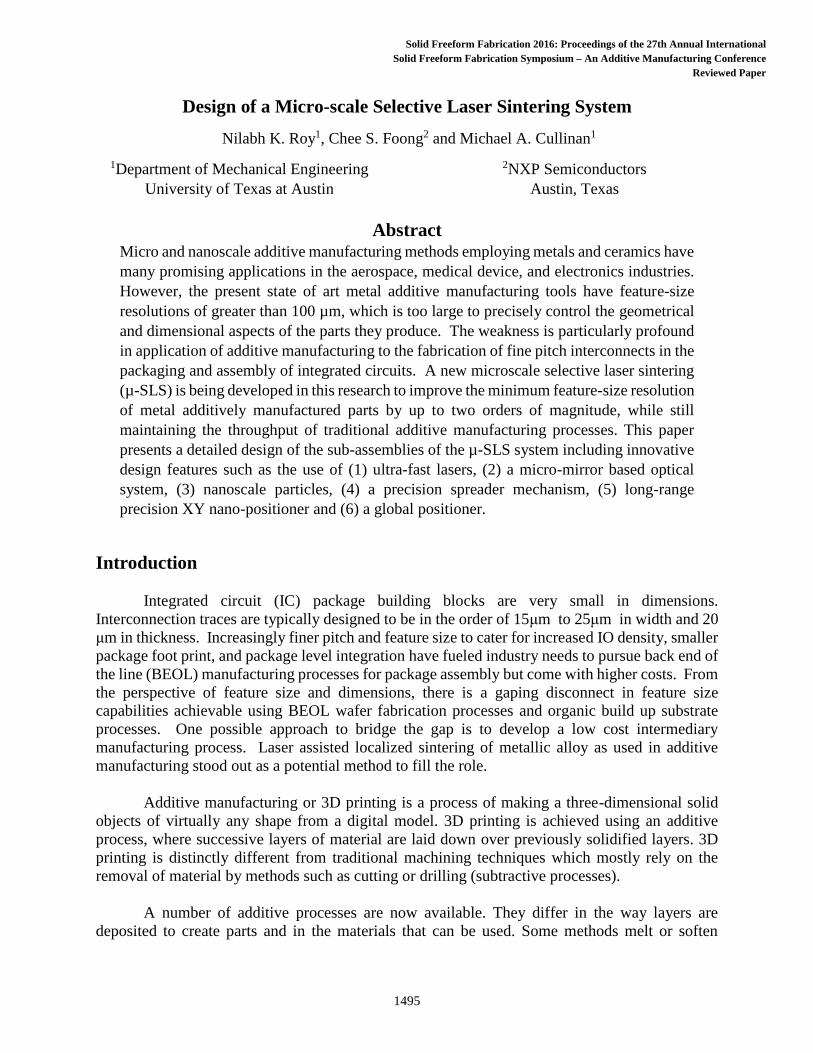
In our present research, a 3D printing process as practiced in the macro-sized domain has been modified and improved to assemble IC packages offering very high volume through put with potential to revolutionize the entire IC backend assembly industry. The gist of our research and development is to assemble IC packages by fabricating electrical interconnect entities and dielectric build up layer by layer using a micro selective laser sintering process (µ-SLS). The µ-SLS process and machine we are developing works well with many metals and their alloys. We are using µ-SLS to manufacture IC packaging building blocks such as –
- Conducting traces / wires - Inter-layer vias - Wire bond finger pads - C4 bump pads - BGA pads - Power and ground planes - Flip Chip C4 pillar bumps - Antennas - Passive Components
Figure 1. IC Package and Assembly Interconnect Building Blocks
µ-SLS replaces the semi additive copper plating / etching process typically employed to build up IC package substrate redistribution layers. In addition to building the network of conductive interconnecting layers, the µ-SLS can be used to form electrical connection between the sintered terminals of the conductive traces and interconnection pads on IC chips and between layers. The µ-SLS process described in this paper is a completely additive process where the required interconnect entities in their final form and functions are made at locations where they are needed on the package.
The scope of our present research encompasses four distinctly unique but interdependent areas. In order to accomplish the objectives as laid out above, the team is working on 1) Development of Copper Nanoparticle Inks 2) Physical and Thermal Modeling of Laser-Ink Interaction and Sintering 3) Micro Laser Sintering Process Development and Characterization and 4) Laser and Machine Design and Automation.
1496
We set out to demonstrate the feasibility of fabricating 3D laser sintered copper pillar
bumps on flip chip devices focusing on pillars with high aspect ratio (> 2:1), smaller diameter (< 5µm), and pillar pitch (< 20µm) in near net-shape features. Following that, we extend the process capabilities to enable a low cost and mask-less fabrication process for multi-layer redistribution layer (RDL) with design features comparable to electroplating process for wafer level chip scale device package (WLCSP). Next, we formulate and demonstrate the new fabrication technology as a feasible low cost and high volume manufacturing alternative for IC interconnect process and for the emerging low cost packaging needs of internet of things (IoT) and wearables markets. And finally, we explore further other potential applications of the fabrication technology in fast IC packaging prototypes, on-chip low R interconnect, customizable IC packages, MEMs sensor design and packaging, and roll-to-roll printed electronics. In this paper, we focus on the design of the laser systems, machine design, and automation aspects of the research. Design of the µ-SLS system
A) Laser and optics
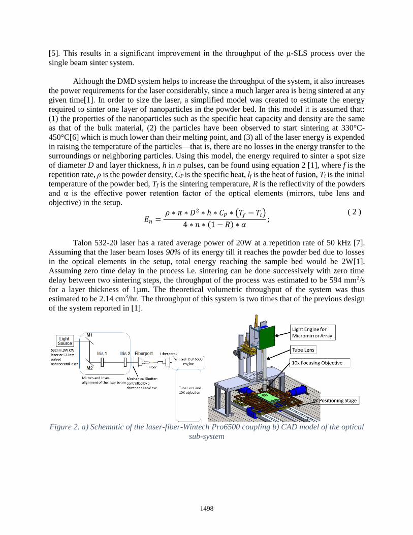
The first prototype of the µ-SLS uses a 3W CW laser (532nm) from Lasever, Inc. To achieve precise control over the heat-affected zone of the micro-SLS powder bed, the current laser will be replaced with a nanosecond laser, Talon 532-20 from Spectra Physics with a 25ns pulse duration. Optical components in the setup including mirrors, Digital micro-mirror device (Pro6500 DMD from Wintech), mechanical shutter and objective lens have been designed keeping in mind the possible need of replacing the nanosecond laser with ultra-fast lasers such as picosecond and femtosecond lasers at later stages of product development. Traditionally, for macroscale selective laser sintering system, the optics typically consisted of a set of beam expanders, a few reflection mirrors, and a 3-axis dynamic scanner or an fθ lens and an x-y galvanometric mirror[1]. However, in order to get down to a spot size of 1 μm additional focusing optics are required. One major
drawback of focusing the laser spot down to spot of 1 μm from a spot of 100 μm is that the
throughput of the system is reduced by a factor of 10,000. To overcome this problem and increase the throughput of the process, a digital micro-mirror device (DMD), Pro6500 from Wintech, was used to replace the traditional galvanometric mirror in macroscale SLS systems. The micro-mirror pixels are 7 μm by 7 μm in size and are placed 600nm apart[2]. The laser is coupled to the DMD engine via a fiber coupling setup (shown in Figure 1) with a mechanical shutter (VS14 from Vincent Associates) to modulate the exposure time. The incident laser beam into the DMD is then expanded using a fisheye lens and directed off the micro-mirror array through a 10X infinity corrected long working distance objective lens from Mitutoyo. The objective lens has an NA of 0.28 and a theoretical resolving power of 604nm with a Gaussian beam of 532nm wavelength. The resolving power of an objective lens for a Gaussian beam is given by equation 1 [3],
𝑅𝑒𝑠𝑜𝑙𝑣𝑖𝑛𝑔 𝑝𝑜𝑤𝑒𝑟 =𝜆
𝜋 ∗ 𝑁𝐴
( 1 )
where, 𝜆 is the wavelength of the light and NA is the numerical aperture of the objective lens. This allows each 7.6 µm by 7.6 µm pixel in the micro-mirror array to be focused down to a spot size of approximately 1µm. The DMD chipset selected consists of an array of 1920 by 1080 individually addressable micro-mirrors with a binary pattern rate of up to 5 kHz [4]. Therefore, the incident laser beam can be split into a total of 2,073,600 individual beams with a feature size of 1μm each
1497
[5]. This results in a significant improvement in the throughput of the μ-SLS process over the single beam sinter system.
Although the DMD system helps to increase the throughput of the system, it also increases the power requirements for the laser considerably, since a much larger area is being sintered at any given time[1]. In order to size the laser, a simplified model was created to estimate the energy required to sinter one layer of nanoparticles in the powder bed. In this model it is assumed that: (1) the properties of the nanoparticles such as the specific heat capacity and density are the same as that of the bulk material, (2) the particles have been observed to start sintering at 330°C-450°C[6] which is much lower than their melting point, and (3) all of the laser energy is expended in raising the temperature of the particles—that is, there are no losses in the energy transfer to the surroundings or neighboring particles. Using this model, the energy required to sinter a spot size of diameter D and layer thickness, h in n pulses, can be found using equation 2 [1], where f is the repetition rate, ρ is the powder density, CP is the specific heat, lf is the heat of fusion, Ti is the initial temperature of the powder bed, Tf is the sintering temperature, R is the reflectivity of the powders and α is the effective power retention factor of the optical elements (mirrors, tube lens and
objective) in the setup.
𝐸𝑛 = 𝜌 ∗ 𝜋 ∗ 𝐷2 ∗ ℎ ∗ 𝐶𝑃 ∗ (𝑇𝑓 − 𝑇𝑖)
4 ∗ 𝑛 ∗ (1 − 𝑅) ∗ 𝛼;
( 2 )
Talon 532-20 laser has a rated average power of 20W at a repetition rate of 50 kHz [7].
Assuming that the laser beam loses 90% of its energy till it reaches the powder bed due to losses in the optical elements in the setup, total energy reaching the sample bed would be 2W[1]. Assuming zero time delay in the process i.e. sintering can be done successively with zero time delay between two sintering steps, the throughput of the process was estimated to be 594 mm2/s for a layer thickness of 1µm. The theoretical volumetric throughput of the system was thus estimated to be 2.14 cm3/hr. The throughput of this system is two times that of the previous design of the system reported in [1].
Figure 2. a) Schematic of the laser-fiber-Wintech Pro6500 coupling b) CAD model of the optical
sub-system
1498
B) Use of nanoparticles
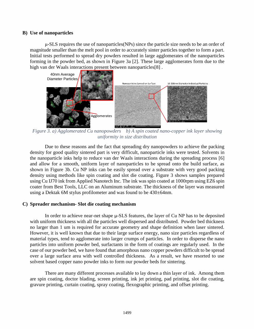
μ-SLS requires the use of nanoparticles(NPs) since the particle size needs to be an order of magnitude smaller than the melt pool in order to accurately sinter particles together to form a part. Initial tests performed to spread dry powders resulted in large agglomerates of the nanoparticles forming in the powder bed, as shown in Figure 3a [2]. These large agglomerates form due to the high van der Waals interactions present between nanoparticles[8] .
Figure 3. a) Agglomerated Cu nanopowders b) A spin coated nano-copper ink layer showing
uniformity in size distribution
Due to these reasons and the fact that spreading dry nanopowders to achieve the packing density for good quality sintered part is very difficult, nanoparticle inks were tested. Solvents in the nanoparticle inks help to reduce van der Waals interactions during the spreading process [6] and allow for a smooth, uniform layer of nanoparticles to be spread onto the build surface, as shown in Figure 3b. Cu NP inks can be easily spread over a substrate with very good packing density using methods like spin coating and slot die coating. Figure 3 shows samples prepared using Cu IJ70 ink from Applied Nanotech Inc. The ink was spin coated at 1000rpm using EZ6 spin coater from Best Tools, LLC on an Aluminum substrate. The thickness of the layer was measured using a Dektak 6M stylus profilometer and was found to be 430±64nm.
C) Spreader mechanism- Slot die coating mechanism
In order to achieve near-net shape µ-SLS features, the layer of Cu NP has to be deposited with uniform thickness with all the particles well dispersed and distributed. Powder bed thickness no larger than 1 um is required for accurate geometry and shape definition when laser sintered. However, it is well known that due to their large surface energy, nano size particles regardless of material types, tend to agglomerate into larger crumps of particles. In order to disperse the nano particles into uniform powder bed, surfactants in the form of coatings are regularly used. In the case of our powder bed, we have found that amorphous nano copper powders difficult to be spread over a large surface area with well controlled thickness. As a result, we have resorted to use solvent based copper nano powder inks to form our powder beds for sintering.
There are many different processes available to lay down a thin layer of ink. Among them are spin coating, doctor blading, screen printing, ink jet printing, pad printing, slot die coating, gravure printing, curtain coating, spray coating, flexographic printing, and offset printing.
40nm Average Diameter Particles
Agglomerates
1499
Slot die coating method has been adopted because it is a very flexible and adaptable process highly suitable for the development work we are undertaking. Such a slot die coating system is advantages because it is able to coat organic or inorganic liquids on flexible or rigid substrates with excellent coating uniformity (typically ±3% or better). The slot die coating system we are working on is able to deposit a wide range of thicknesses ranging from 20nm to 150μm. Our slot
die coating system is also capable of coating a wide range of process materials with varying viscosities.
From the high volume manufacturing perspective, the slot die coating process is also very
attractive because it has high efficiency with over 95% material utilization. In addition to being a very high throughput, the slot die coating process can be easily adapted for roll-to-roll processing which will further improve the overall productivity.
Slot die coating technology has been used to deposit a variety of liquid chemistries onto glass, stainless steel, and plastic substrates for the development and production of a broad range of applications such as flat panel displays (including LCD, OLED, flexible, and others), photovoltaic panels (such as CIGS, CdTe, OPV, and others), solid state lighting (OLED and LED), and various organic and printed electronic applications such as RFID, polymer batteries, sensors and others. This is achieved through the precise metering of the process fluid and dispensing it at a controlled rate while the coating die is precisely moved relative to the substrate.
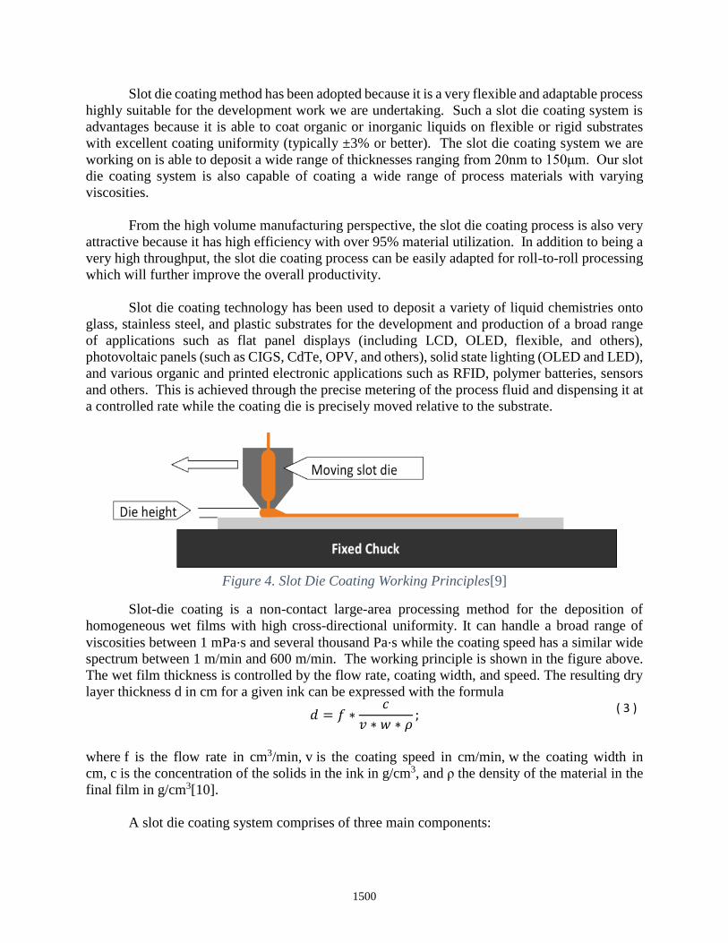
Figure 4. Slot Die Coating Working Principles[9]
Slot-die coating is a non-contact large-area processing method for the deposition of homogeneous wet films with high cross-directional uniformity. It can handle a broad range of viscosities between 1 mPa⋅s and several thousand Pa⋅s while the coating speed has a similar wide spectrum between 1 m/min and 600 m/min. The working principle is shown in the figure above. The wet film thickness is controlled by the flow rate, coating width, and speed. The resulting dry layer thickness d in cm for a given ink can be expressed with the formula
𝑑 = 𝑓 ∗
𝑐
𝑣 ∗ 𝑤 ∗ 𝜌; ( 3 )
where f is the flow rate in cm3/min, v is the coating speed in cm/min, w the coating width in cm, c is the concentration of the solids in the ink in g/cm3, and ρ the density of the material in the final film in g/cm3[10].
A slot die coating system comprises of three main components:
1500
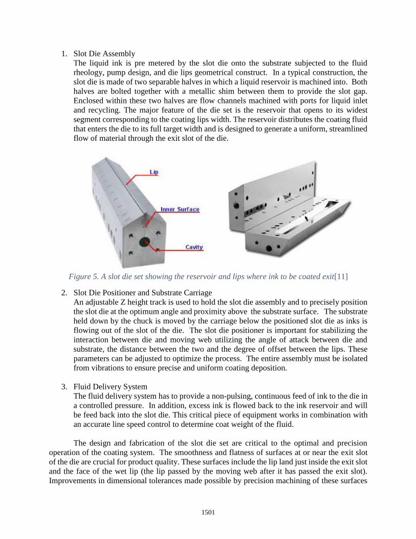
1. Slot Die Assembly The liquid ink is pre metered by the slot die onto the substrate subjected to the fluid rheology, pump design, and die lips geometrical construct. In a typical construction, the slot die is made of two separable halves in which a liquid reservoir is machined into. Both halves are bolted together with a metallic shim between them to provide the slot gap. Enclosed within these two halves are flow channels machined with ports for liquid inlet and recycling. The major feature of the die set is the reservoir that opens to its widest segment corresponding to the coating lips width. The reservoir distributes the coating fluid that enters the die to its full target width and is designed to generate a uniform, streamlined flow of material through the exit slot of the die.
Figure 5. A slot die set showing the reservoir and lips where ink to be coated exit[11]
2. Slot Die Positioner and Substrate Carriage An adjustable Z height track is used to hold the slot die assembly and to precisely position the slot die at the optimum angle and proximity above the substrate surface. The substrate held down by the chuck is moved by the carriage below the positioned slot die as inks is flowing out of the slot of the die. The slot die positioner is important for stabilizing the interaction between die and moving web utilizing the angle of attack between die and substrate, the distance between the two and the degree of offset between the lips. These parameters can be adjusted to optimize the process. The entire assembly must be isolated from vibrations to ensure precise and uniform coating deposition.
3. Fluid Delivery System The fluid delivery system has to provide a non-pulsing, continuous feed of ink to the die in a controlled pressure. In addition, excess ink is flowed back to the ink reservoir and will be feed back into the slot die. This critical piece of equipment works in combination with an accurate line speed control to determine coat weight of the fluid.
The design and fabrication of the slot die set are critical to the optimal and precision
operation of the coating system. The smoothness and flatness of surfaces at or near the exit slot of the die are crucial for product quality. These surfaces include the lip land just inside the exit slot and the face of the wet lip (the lip passed by the moving web after it has passed the exit slot). Improvements in dimensional tolerances made possible by precision machining of these surfaces
1501
may seem miniscule, but in applications involving high volumes or costly coating materials, the economic gains can be great. The effect of flatness variations becomes progressively greater as coating weights become smaller.
The slot die coating method offers higher line speed capability and greater coat weight uniformity provided that the coating system as a whole must be designed to exacting tolerances based of the rheological characteristics of the fluid. The slot die can then achieve defect-free coatings with increased production speeds, positive coat weight control, controlled cross-web distribution and improved waste management.
D) Long range XY nanopositioner
A long range XY nano-positioner is employed to align the sample wafer under the objective lens of the optical system and to scan the sample under the micro-mirror based optical system with sub-micron accuracy and repeatability. Due to absence of friction and backlash, flexure-based compliant guiding mechanisms have been widely employed in applications requiring precision motion. The micro-mirror based optical sub-system can only pattern an area of 2mm by 1mm at once and thus, the wafer has to be moved under the sub-system to pattern the entire 2” by 2” area.
Consequently, the need to have the range of the system to be 2” along X and Y directions. Selection
of an actuator for this application is vital to achieve the 2” range with sub-micron accuracy. Electromagnetic actuators or voice coil actuators (VCAs) are widely used in long-travel, flexure-based parallel XY stages since VCAs are capable of delivering a frictionless inch-level stroke along with a fine resolution.
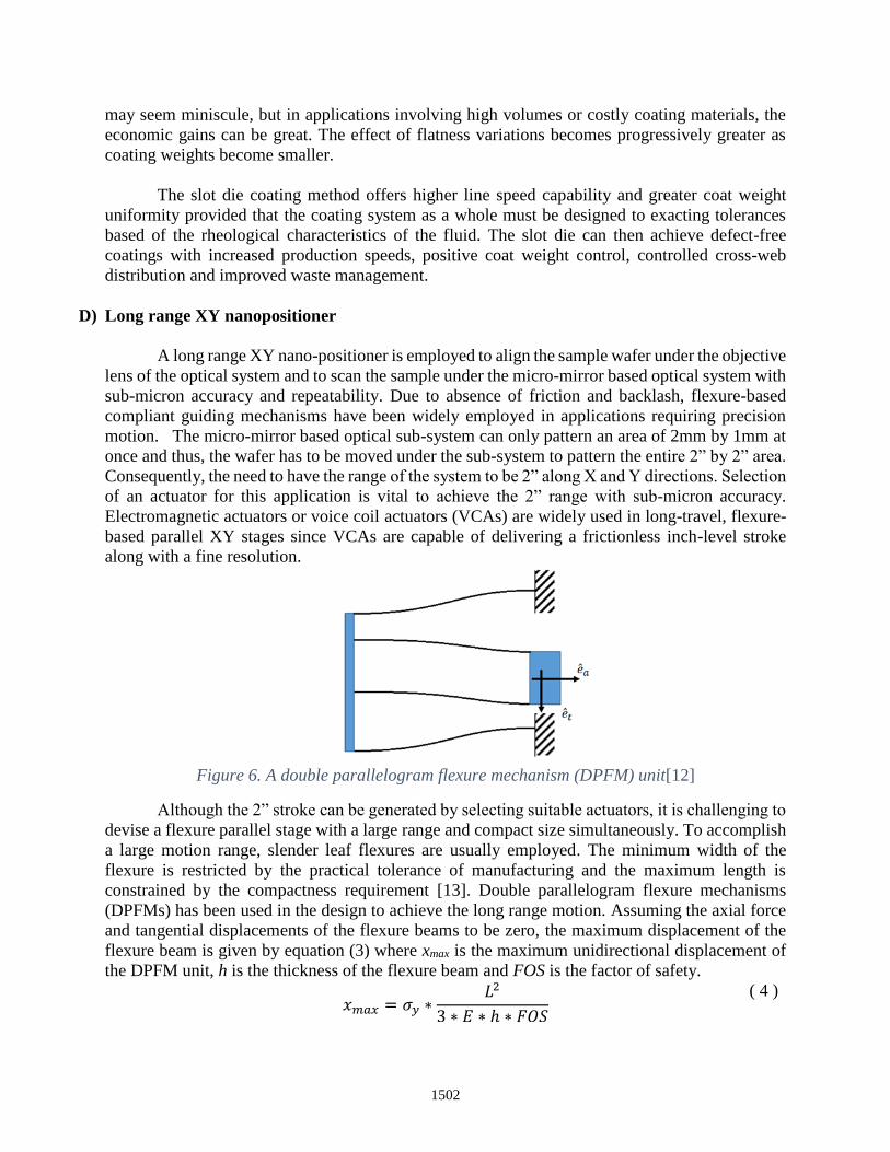
Figure 6. A double parallelogram flexure mechanism (DPFM) unit[12]
Although the 2” stroke can be generated by selecting suitable actuators, it is challenging to
devise a flexure parallel stage with a large range and compact size simultaneously. To accomplish a large motion range, slender leaf flexures are usually employed. The minimum width of the flexure is restricted by the practical tolerance of manufacturing and the maximum length is constrained by the compactness requirement [13]. Double parallelogram flexure mechanisms (DPFMs) has been used in the design to achieve the long range motion. Assuming the axial force and tangential displacements of the flexure beams to be zero, the maximum displacement of the flexure beam is given by equation (3) where xmax is the maximum unidirectional displacement of the DPFM unit, h is the thickness of the flexure beam and FOS is the factor of safety.
𝑥𝑚𝑎𝑥 = 𝜎𝑦 ∗𝐿2
3 ∗ 𝐸 ∗ ℎ ∗ 𝐹𝑂𝑆
( 4 )
1502
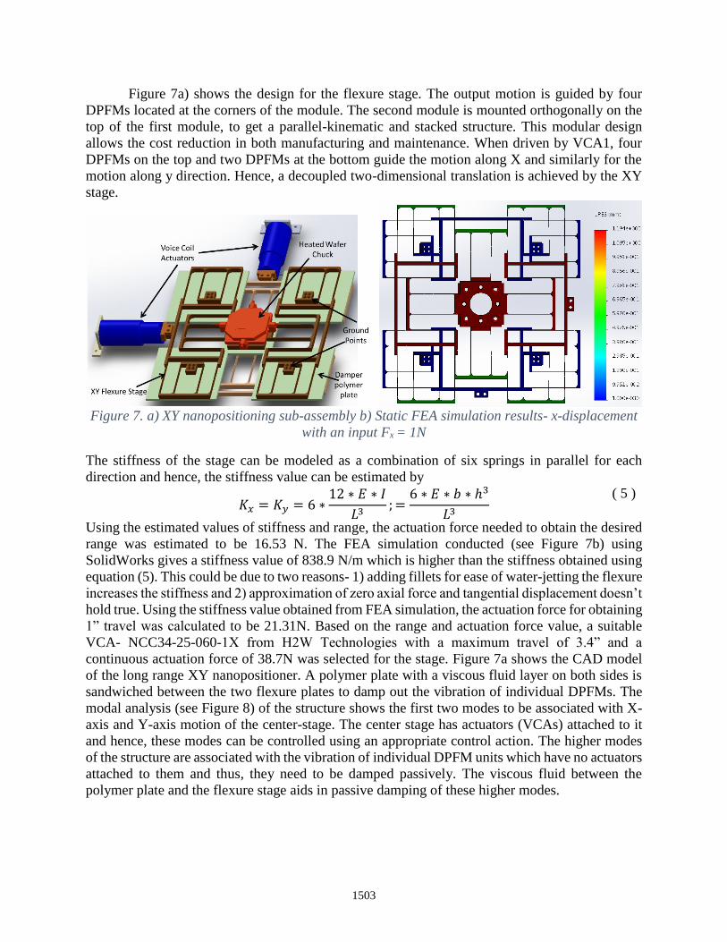
Figure 7a) shows the design for the flexure stage. The output motion is guided by four DPFMs located at the corners of the module. The second module is mounted orthogonally on the top of the first module, to get a parallel-kinematic and stacked structure. This modular design allows the cost reduction in both manufacturing and maintenance. When driven by VCA1, four DPFMs on the top and two DPFMs at the bottom guide the motion along X and similarly for the motion along y direction. Hence, a decoupled two-dimensional translation is achieved by the XY stage.
Figure 7. a) XY nanopositioning sub-assembly b) Static FEA simulation results- x-displacement
with an input Fx = 1N
The stiffness of the stage can be modeled as a combination of six springs in parallel for each direction and hence, the stiffness value can be estimated by
𝐾𝑥 = 𝐾𝑦 = 6 ∗12 ∗ 𝐸 ∗ 𝐼
𝐿3; =
6 ∗ 𝐸 ∗ 𝑏 ∗ ℎ3
𝐿3
( 5 )
Using the estimated values of stiffness and range, the actuation force needed to obtain the desired range was estimated to be 16.53 N. The FEA simulation conducted (see Figure 7b) using SolidWorks gives a stiffness value of 838.9 N/m which is higher than the stiffness obtained using equation (5). This could be due to two reasons- 1) adding fillets for ease of water-jetting the flexure increases the stiffness and 2) approximation of zero axial force and tangential displacement doesn’t hold true. Using the stiffness value obtained from FEA simulation, the actuation force for obtaining 1” travel was calculated to be 21.31N. Based on the range and actuation force value, a suitable VCA- NCC34-25-060-1X from H2W Technologies with a maximum travel of 3.4” and a
continuous actuation force of 38.7N was selected for the stage. Figure 7a shows the CAD model of the long range XY nanopositioner. A polymer plate with a viscous fluid layer on both sides is sandwiched between the two flexure plates to damp out the vibration of individual DPFMs. The modal analysis (see Figure 8) of the structure shows the first two modes to be associated with X-axis and Y-axis motion of the center-stage. The center stage has actuators (VCAs) attached to it and hence, these modes can be controlled using an appropriate control action. The higher modes of the structure are associated with the vibration of individual DPFM units which have no actuators attached to them and thus, they need to be damped passively. The viscous fluid between the polymer plate and the flexure stage aids in passive damping of these higher modes.
1503
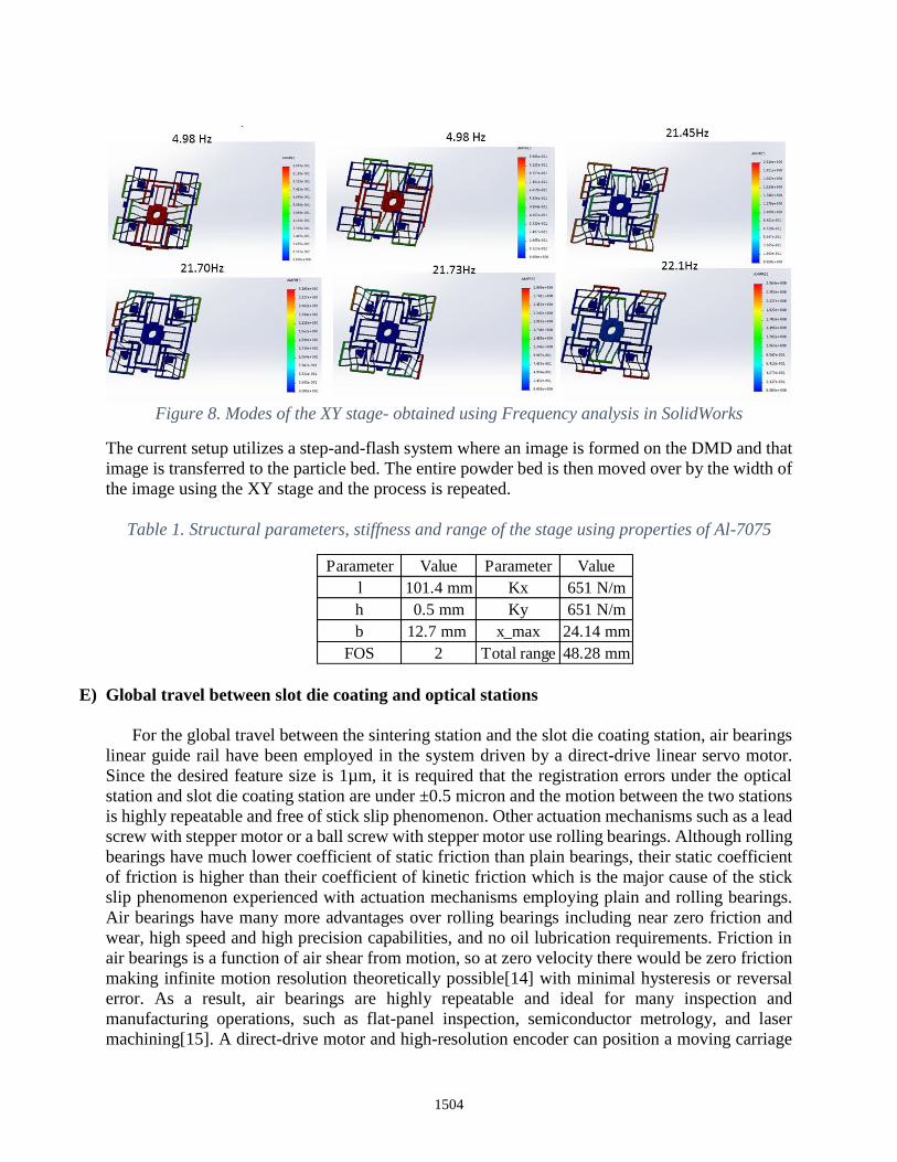
Figure 8. Modes of the XY stage- obtained using Frequency analysis in SolidWorks
The current setup utilizes a step-and-flash system where an image is formed on the DMD and that image is transferred to the particle bed. The entire powder bed is then moved over by the width of the image using the XY stage and the process is repeated.
Table 1. Structural parameters, stiffness and range of the stage using properties of Al-7075
E) Global travel between slot die coating and optical stations For the global travel between the sintering station and the slot die coating station, air bearings
linear guide rail have been employed in the system driven by a direct-drive linear servo motor. Since the desired feature size is 1µm, it is required that the registration errors under the optical station and slot die coating station are under ±0.5 micron and the motion between the two stations is highly repeatable and free of stick slip phenomenon. Other actuation mechanisms such as a lead screw with stepper motor or a ball screw with stepper motor use rolling bearings. Although rolling bearings have much lower coefficient of static friction than plain bearings, their static coefficient of friction is higher than their coefficient of kinetic friction which is the major cause of the stick slip phenomenon experienced with actuation mechanisms employing plain and rolling bearings. Air bearings have many more advantages over rolling bearings including near zero friction and wear, high speed and high precision capabilities, and no oil lubrication requirements. Friction in air bearings is a function of air shear from motion, so at zero velocity there would be zero friction making infinite motion resolution theoretically possible[14] with minimal hysteresis or reversal error. As a result, air bearings are highly repeatable and ideal for many inspection and manufacturing operations, such as flat-panel inspection, semiconductor metrology, and laser machining[15]. A direct-drive motor and high-resolution encoder can position a moving carriage
Parameter Value Parameter Valuel 101.4 mm Kx 651 N/mh 0.5 mm Ky 651 N/mb 12.7 mm x_max 24.14 mm
FOS 2 Total range 48.28 mm
1504
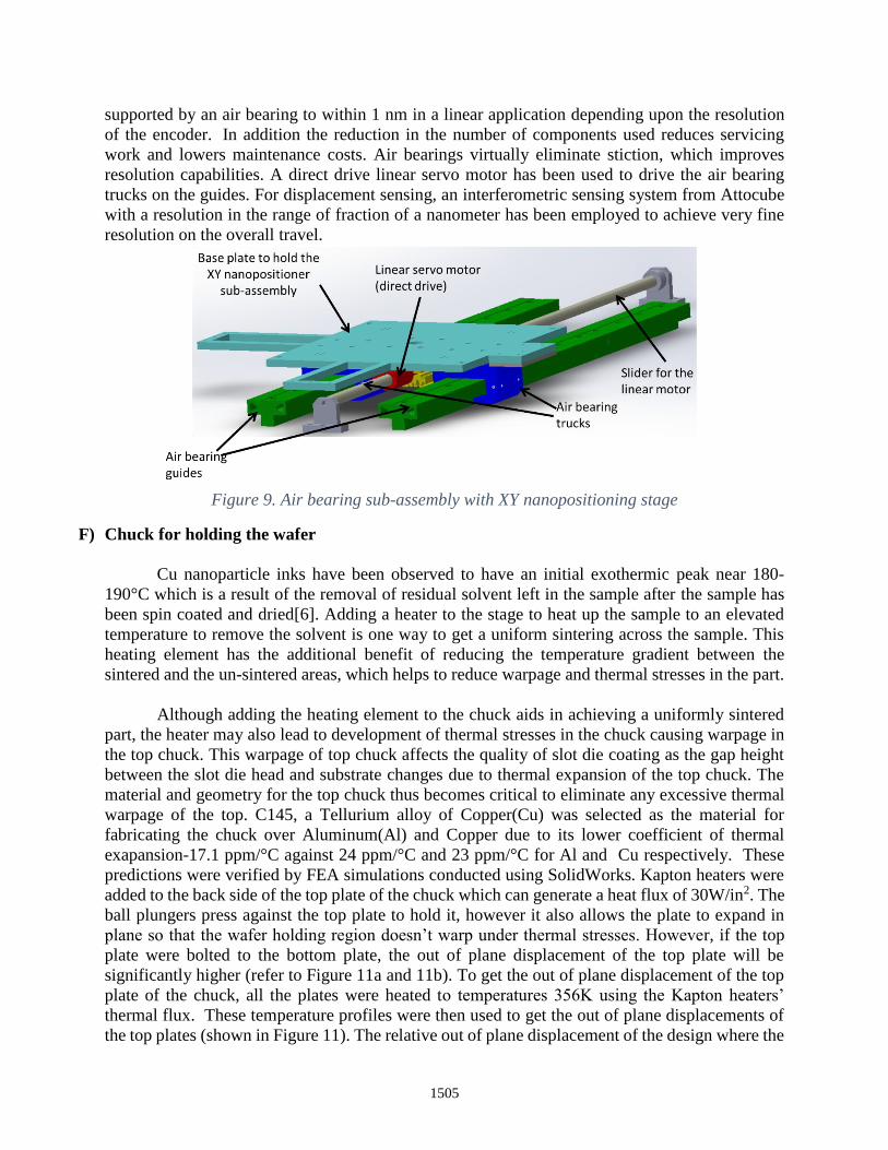
supported by an air bearing to within 1 nm in a linear application depending upon the resolution of the encoder. In addition the reduction in the number of components used reduces servicing work and lowers maintenance costs. Air bearings virtually eliminate stiction, which improves resolution capabilities. A direct drive linear servo motor has been used to drive the air bearing trucks on the guides. For displacement sensing, an interferometric sensing system from Attocube with a resolution in the range of fraction of a nanometer has been employed to achieve very fine resolution on the overall travel.
Figure 9. Air bearing sub-assembly with XY nanopositioning stage
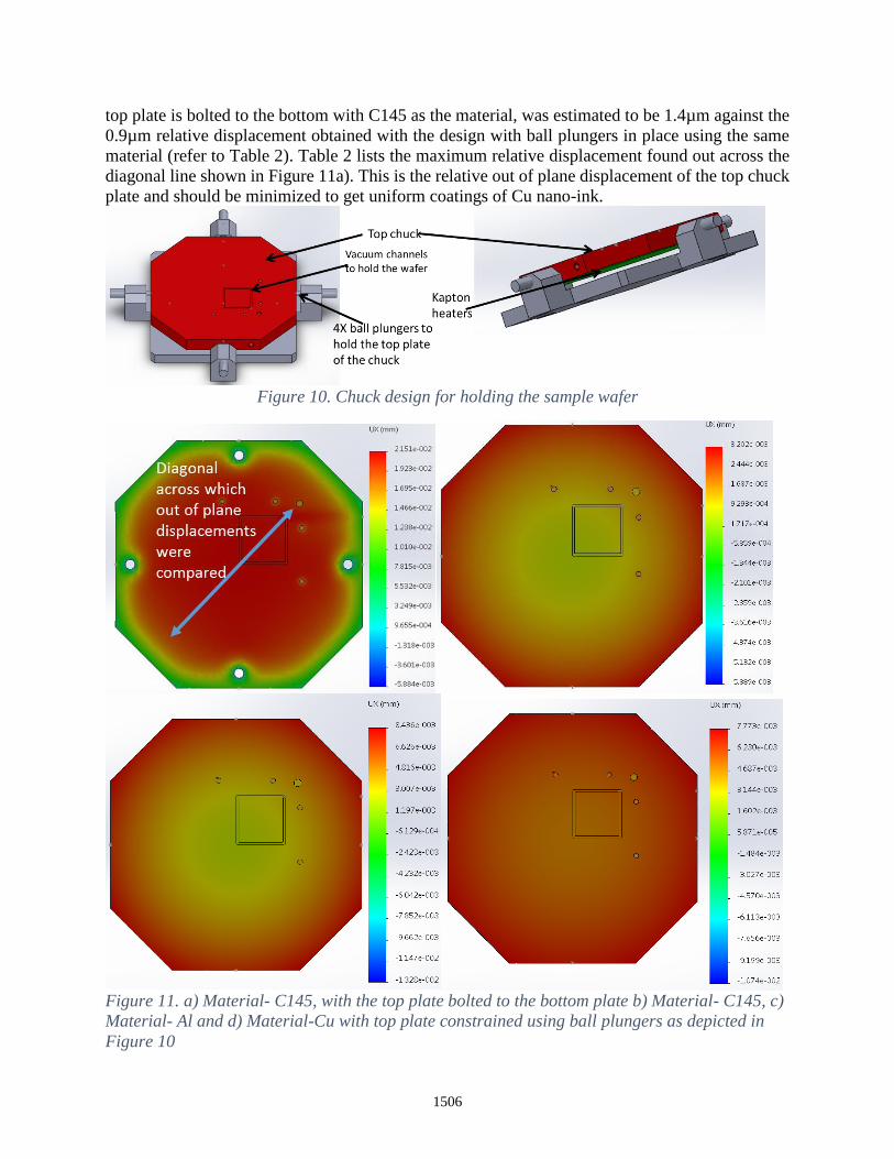
F) Chuck for holding the wafer
Cu nanoparticle inks have been observed to have an initial exothermic peak near 180-190°C which is a result of the removal of residual solvent left in the sample after the sample has been spin coated and dried[6]. Adding a heater to the stage to heat up the sample to an elevated temperature to remove the solvent is one way to get a uniform sintering across the sample. This heating element has the additional benefit of reducing the temperature gradient between the sintered and the un-sintered areas, which helps to reduce warpage and thermal stresses in the part.
Although adding the heating element to the chuck aids in achieving a uniformly sintered part, the heater may also lead to development of thermal stresses in the chuck causing warpage in the top chuck. This warpage of top chuck affects the quality of slot die coating as the gap height between the slot die head and substrate changes due to thermal expansion of the top chuck. The material and geometry for the top chuck thus becomes critical to eliminate any excessive thermal warpage of the top. C145, a Tellurium alloy of Copper(Cu) was selected as the material for fabricating the chuck over Aluminum(Al) and Copper due to its lower coefficient of thermal exapansion-17.1 ppm/°C against 24 ppm/°C and 23 ppm/°C for Al and Cu respectively. These predictions were verified by FEA simulations conducted using SolidWorks. Kapton heaters were added to the back side of the top plate of the chuck which can generate a heat flux of 30W/in2. The ball plungers press against the top plate to hold it, however it also allows the plate to expand in plane so that the wafer holding region doesn’t warp under thermal stresses. However, if the top plate were bolted to the bottom plate, the out of plane displacement of the top plate will be significantly higher (refer to Figure 11a and 11b). To get the out of plane displacement of the top plate of the chuck, all the plates were heated to temperatures 356K using the Kapton heaters’
thermal flux. These temperature profiles were then used to get the out of plane displacements of the top plates (shown in Figure 11). The relative out of plane displacement of the design where the
1505
top plate is bolted to the bottom with C145 as the material, was estimated to be 1.4µm against the 0.9µm relative displacement obtained with the design with ball plungers in place using the same material (refer to Table 2). Table 2 lists the maximum relative displacement found out across the diagonal line shown in Figure 11a). This is the relative out of plane displacement of the top chuck plate and should be minimized to get uniform coatings of Cu nano-ink.
Figure 10. Chuck design for holding the sample wafer
Figure 11. a) Material- C145, with the top plate bolted to the bottom plate b) Material- C145, c)
Material- Al and d) Material-Cu with top plate constrained using ball plungers as depicted in
Figure 10
1506
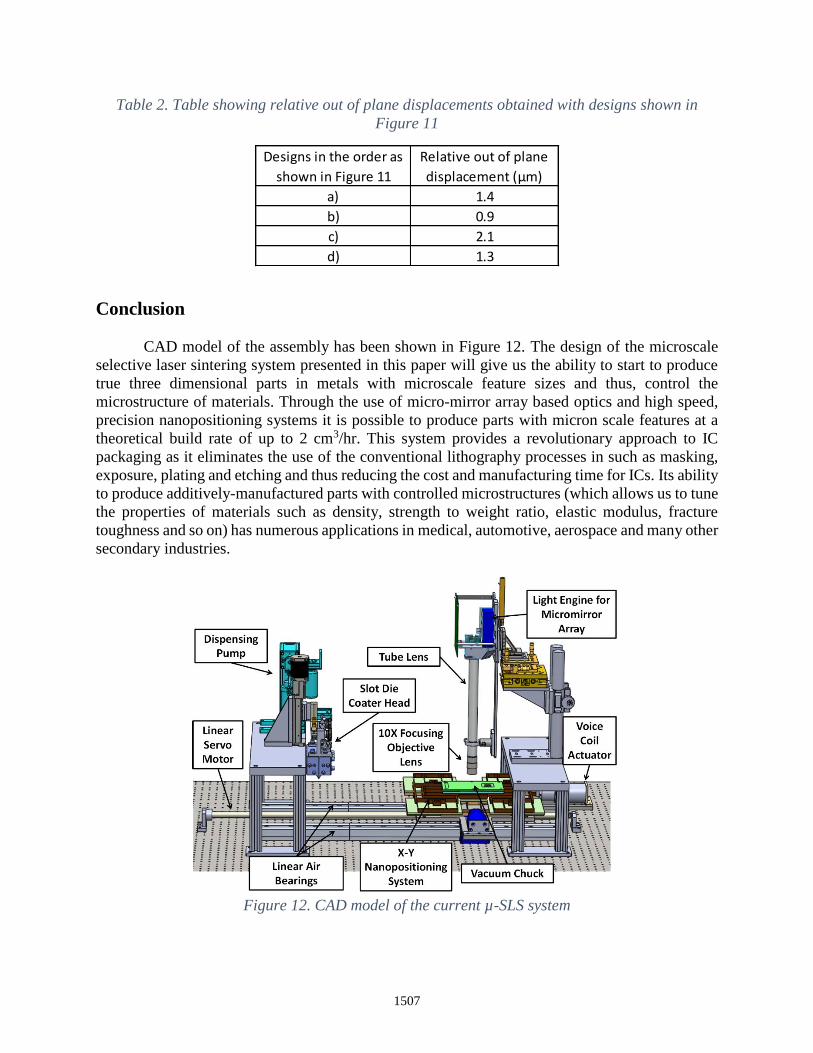
Table 2. Table showing relative out of plane displacements obtained with designs shown in
Figure 11
Conclusion
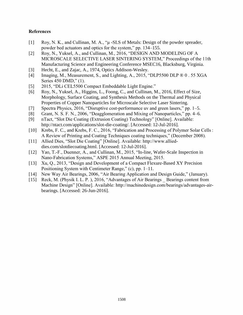
CAD model of the assembly has been shown in Figure 12. The design of the microscale selective laser sintering system presented in this paper will give us the ability to start to produce true three dimensional parts in metals with microscale feature sizes and thus, control the microstructure of materials. Through the use of micro-mirror array based optics and high speed, precision nanopositioning systems it is possible to produce parts with micron scale features at a theoretical build rate of up to 2 cm3/hr. This system provides a revolutionary approach to IC packaging as it eliminates the use of the conventional lithography processes in such as masking, exposure, plating and etching and thus reducing the cost and manufacturing time for ICs. Its ability to produce additively-manufactured parts with controlled microstructures (which allows us to tune the properties of materials such as density, strength to weight ratio, elastic modulus, fracture toughness and so on) has numerous applications in medical, automotive, aerospace and many other secondary industries.
Figure 12. CAD model of the current µ-SLS system
a) 1.4
b) 0.9
c) 2.1
d) 1.3
Designs in the order as
shown in Figure 11
Relative out of plane
displacement (μm)
1507
References
[1] Roy, N. K., and Cullinan, M. A., “μ -SLS of Metals: Design of the powder spreader, powder bed actuators and optics for the system,” pp. 134–155.
[2] Roy, N., Yuksel, A., and Cullinan, M., 2016, “DESIGN AND MODELING OF A
MICROSCALE SELECTIVE LASER SINTERING SYSTEM,” Proceedings of the 11th
Manufacturing Science and Engineering Conference MSEC16, Blacksburg, Virginia. [3] Hecht, E., and Zajac, A., 1974, Optics Addison-Wesley. [4] Imaging, M., Measurement, S., and Lighting, A., 2015, “DLP5500 DLP ® 0 . 55 XGA
Series 450 DMD,” (1). [5] 2015, “DLi CEL5500 Compact Embeddable Light Engine.” [6] Roy, N., Yuksel, A., Higgins, L., Foong, C., and Cullinan, M., 2016, Effect of Size,
Morphology, Surface Coating, and Synthesis Methods on the Thermal and Physical Properties of Copper Nanoparticles for Microscale Selective Laser Sintering.
[7] Spectra Physics, 2016, “Disruptive cost-performance uv and green lasers,” pp. 1–5. [8] Grant, N. S. F. N., 2006, “Deagglomeration and Mixing of Nanoparticles,” pp. 4–6. [9] nTact, “Slot Die Coating (Extrusion Coating) Technology” [Online]. Available:
http://ntact.com/applications/slot-die-coating/. [Accessed: 12-Jul-2016]. [10] Krebs, F. C., and Krebs, F. C., 2016, “Fabrication and Processing of Polymer Solar Cells :
A Review of Printing and Coating Techniques coating techniques,” (December 2008). [11] Allied Dies, “Slot Die Coating” [Online]. Available: http://www.allied-
dies.com/slotdiecoating.html. [Accessed: 12-Jul-2016]. [12] Yao, T.-F., Duenner, A., and Cullinan, M., 2015, “In-line, Wafer-Scale Inspection in
Nano-Fabrication Systems,” ASPE 2015 Annual Meeting, 2015. [13] Xu, Q., 2013, “Design and Development of a Compact Flexure-Based XY Precision
Positioning System with Centimeter Range,” (c), pp. 1–11. [14] New Way Air Bearings, 2006, “Air Bearing Application and Design Guide,” (January). [15] Reck, M. (Physik I. L. P. ), 2016, “Advantages of Air Bearings _ Bearings content from
Machine Design” [Online]. Available: http://machinedesign.com/bearings/advantages-air-bearings. [Accessed: 26-Jun-2016].
1508


![Optimizing selective laser sintering process by grey ...doras.dcu.ie/22813/1/main2.pdf · The selective laser sintering (SLS) was invented in 1989 [1]. In this process, laser employed](https://static.fdocuments.net/doc/165x107/601e4d4954f29749226768bf/optimizing-selective-laser-sintering-process-by-grey-dorasdcuie228131main2pdf.jpg)