DESIGN OF A 16 BIT 10MHZ PIPELINE ADC USING THE SPLIT …
97
DESIGN OF A 16BIT 10MHZ PIPELINE ADC USING THE SPLITADC ARCHITECTURE IN 0.25μ CMOS A Major Qualifying Project submitted to the Faculty of the WORCESTER POLYTECHNIC INSTITUTE in partial fulfillment of the requirements for the Degree of Bachelor of Science in Electrical and Computer Engineering on October 15, 2007 ‐‐‐‐‐‐‐‐‐‐‐‐‐‐‐‐‐‐‐‐‐‐‐‐‐‐‐‐‐‐‐‐ Abhilash Nair Electrical & Computer Engineering Computer Science ‐‐‐‐‐‐‐‐‐‐‐‐‐‐‐‐‐‐‐‐‐‐‐‐‐‐‐‐‐‐‐‐ Sanjeev Goluguri Electrical & Computer Engineering ‐‐‐‐‐‐‐‐‐‐‐‐‐‐‐‐‐‐‐‐‐‐‐‐‐‐‐‐‐‐‐‐ Professor John McNeill Advisor
Transcript of DESIGN OF A 16 BIT 10MHZ PIPELINE ADC USING THE SPLIT …
DESIGN OF A 16BIT 10MHZ PIPELINE ADC USING THE SPLITADC ARCHITECTURE IN
0.25µ CMOS
A Major Qualifying Project
submitted to the Faculty
of the
WORCESTER POLYTECHNIC INSTITUTE
in partial fulfillment of the requirements for the
Degree of Bachelor of Science
in
Electrical and Computer Engineering
on
October 15, 2007
‐‐‐‐‐‐‐‐‐‐‐‐‐‐‐‐‐‐‐‐‐‐‐‐‐‐‐‐‐‐‐‐ Abhilash Nair Electrical & Computer Engineering Computer Science
‐‐‐‐‐‐‐‐‐‐‐‐‐‐‐‐‐‐‐‐‐‐‐‐‐‐‐‐‐‐‐‐
Sanjeev GoluguriElectrical & Computer Engineering
‐‐‐‐‐‐‐‐‐‐‐‐‐‐‐‐‐‐‐‐‐‐‐‐‐‐‐‐‐‐‐‐
Professor John McNeill
Advisor

[i]
Abstract This paper discusses the design of a 16-bit 10MHz pipeline Analog to Digital
Converter (ADC) using the “Split ADC architecture”. A system and circuit level design
of each component of the ADC was created in Cadence. Features of the ADC were
simulated in Matlab to test and examine its basic functionality. Transient analysis of the
system level design was conducted to verify the performance of the ADC. Methods to
correct non-linearities were identified and investigated.

[ii]
Tables of Contents 1. INTRODUCTION ..................................................................................................... 1
2. BACKGROUND INFORMATION ............................................................................... 2
2.1. ANALOG TO DIGITAL CONVERTERS (ADCS) ................................................................... 2
2.2. PIPELINE ADC ......................................................................................................... 5
2.3. PRIOR WORK .......................................................................................................... 8
3. SYSTEM‐LEVEL CHARACTERIZATION OF A PIPELINE ADC ...................................... 10
3.1. LINEAR VS. NON‐LINEAR GAIN STAGE ........................................................................ 10
3.2. NON‐LINEARITY OF SIMULATED ADC ......................................................................... 13
3.3. CUBIC APPROXIMATION OF SIMULATED ADC .............................................................. 14
3.4. CUBIC APPROXIMATION OF SIMULATED DATA FROM CADENCE ....................................... 16
3.5. DIGITAL LOOK‐UP TABLE .......................................................................................... 18
4. CIRCUIT‐LEVEL SIMULATION OF THE ANALOG SUBSYSTEM .................................. 21
4.1. BASIC DIFFERENTIAL PAIR CIRCUIT ............................................................................. 21
4.2. CASCODE DIFF‐PAIR WITH PI‐RESISTOR NETWORK ....................................................... 28
4.3. COMMON MODE FEEDBACK & REPLICA BIAS .............................................................. 36
4.4. DIFF‐PAIR SETTLING TIME ........................................................................................ 41
4.5. SWITCHED CAPACITOR NETWORK .............................................................................. 45
5. QUANTIZER ......................................................................................................... 53
6. CONCLUSION ....................................................................................................... 55

[iii]
7. REFERENCES ........................................................................................................ 56
APPENDIX A: MATLAB CODE ....................................................................................... 57
I. Simulating a linear multi‐stage ADC ................................................................. 57
II. Estimating Vin and ADC error from each stage ................................................ 58
III. Simulating a non‐linear multi stage ADC .......................................................... 59
IV. Simulated data from Cadence showing non‐linearity ...................................... 60
V. Correcting non‐linearity of a simulated multi‐stage ADC ................................. 61
VI. Correcting non‐linearity of simulated data from Cadence ............................... 62
VII. Simulating the basics of a Split‐ADC architecture ............................................. 64
VIII. Simulating non‐linearity from Cadence using Split‐ADC architecture .............. 67
IX. Simulating non‐linearity in the first stage of Split ADC..................................... 70
X. Correcting non‐linearity of a Split‐ADC architecture ........................................ 73
XI. Using Split ADC to test convergence ................................................................. 74
XII. Digital Look Up Table Algorithm ....................................................................... 82
XIII. Analyzing Data .................................................................................................. 83
APPENDIX B: DESIGN OF A BASIC DIFF‐PAIR CIRCUIT FOR VARIOUS VOV ...................... 87
APPENDIX C: DESIGN OF A CASCODE DIFF‐PAIR WITH SPLIT CURRENT APPROACH ..... 88

[iv]
Table of Figures FIGURE 1: BASIC FEATURE OF AN ANALOG TO DIGITAL CONVERSION [2] ............................................. 2
FIGURE 2: ILLUSTRATION OF THE QUANTIZATION PROCESS [2] .......................................................... 3
FIGURE 3: TRANSFER FUNCTION OF AN IDEAL ADC [2] ................................................................... 3
FIGURE 4: SYSTEM BLOCK OF A PIPELINE ADC ............................................................................... 5
FIGURE 5: PRIOR WORK ‐ PROPOSED OPEN LOOP PIPELINE STAGE [4] ............................................... 8
FIGURE 6: OUTPUT CODE OF STAGE 1 ........................................................................................ 10
FIGURE 7: DIFFERENCE BETWEEN A LINEAR AND A NON‐LINEAR GAIN STAGE .................................... 11
FIGURE 8: HISTOGRAM OF CODE LEVELS FOR A LINEAR GAIN STAGE ................................................ 11
FIGURE 9: HISTOGRAM OF CODE LEVELS FOR A NON‐LINEAR GAIN STAGE ........................................ 12
FIGURE 10: DIFFERENCE IN ERROR OF A LINEAR AND NON‐LINEAR GAIN STAGE ................................. 12
FIGURE 11: MEASURING NON‐LINEARITY IN SIMULATED DATA ....................................................... 13
FIGURE 12: CUBIC APPROXIMATION OF SIMULATED DATA ............................................................. 14
FIGURE 13: DIFFERENCE IN NON‐LINEARITY BEFORE AND AFTER CUBIC APPROXIMATION .................... 14
FIGURE 14: CASCODE DIFF‐PAIR WITHOUT COMMON MODE FEEDBACK OR REPLICA BIAS ................... 16
FIGURE 15: CASCODE DIFF‐PAIR WITH COMMON MODE FEEDBACK AND REPLICA BIAS ....................... 16
FIGURE 16: PERCENTAGE ERROR OF DLT ................................................................................... 18
FIGURE 17: ESTIMATED VIN VS. ACTUAL VIN FROM DLT ............................................................... 19
FIGURE 18: ABSOLUTE ERROR FROM DLT ................................................................................... 19
FIGURE 19: STAGE 1 IMPLEMENTATION OF PIPELINE ADC [4] ........................................................ 21
FIGURE 20: CIRCUIT SCHEMATIC OF A SIMPLE DIFF‐PAIR ............................................................... 22

[v]
FIGURE 21: BASIC DIFF‐PAIR OUTPUT CHARACTERISTICS FOR 4 DIFFERENT VOV. ................................ 23
FIGURE 22: RESIDUE PLOT FOR AN OVERDRIVE VOLTAGE OF 150MV ............................................... 25
FIGURE 23: RESIDUE PLOT FOR AN OVERDRIVE VOLTAGE OF 200MV ............................................... 25
FIGURE 24: RESIDUE PLOT FOR AN OVERDRIVE VOLTAGE OF 250MV ............................................... 26
FIGURE 25: RESIDUE PLOT FOR AN OVERDRIVE VOLTAGE OF 300MV ............................................... 26
FIGURE 26: BASIC DIFF‐PAIR OUTPUT VERSUS INPUT FOR VARIOUS OVERDRIVE VOLTAGES .................. 28
FIGURE 27: ILLUSTRATION OF CASCODE HIGH OUTPUT IMPEDANCE ................................................. 29
FIGURE 28: SIMPLE COMMON SOURCE CIRCUIT ........................................................................... 30
FIGURE 29: CASCODED COMMON SOURCE CIRCUIT ...................................................................... 30
FIGURE 30: COMPARISON OF CASCODE AND NON‐CASCODE DIFF‐PAIR OUTPUT CHARACTERISTICS ....... 30
FIGURE 31: SMALL SIGNAL GAIN COMPARISON OF CASCODE AND NON‐CASCODE DIFF‐PAIR ............... 31
FIGURE 32: CASCODE DIFF‐PAIR WITH PI‐RESISTOR NETWORK ....................................................... 32
FIGURE 33: CASCODED DIFF‐PAIR DIFFERENTIAL OUTPUT VERSUS INPUT CHARACTERISTIC ................... 33
FIGURE 34: CASCODED DIFF‐PAIR RESIDUE PLOT ......................................................................... 34
FIGURE 35: CIRCUIT SCHEMATIC OF CASCODED DIFF‐PAIR WITH CMFB AND REPLICA BIAS ................. 37
FIGURE 36: BIAS CIRCUIT FOR DIFF‐PAIR AND CMFB ................................................................... 38
FIGURE 37: OUTPUT VS. INPUT FOR CASCODE DIFF‐PAIR WITH CMFB AND REPLICA BIAS ................... 39
FIGURE 38: DIFFERENTIAL OUTPUT VERSUS DIFFERENTIAL INPUT FOR CASCODE DIFF‐PAIR WITH CMFB 40
FIGURE 39: OPERATING POINT GAIN FOR A CASCODE DIFF‐PAIR WITH CMFB & REPLICA BIAS ............. 40
FIGURE 40: TEST CIRCUIT FOR MEASURING SETTLING TIME OF DIFF‐PAIR ......................................... 41
FIGURE 41: SETTING TIME PERFORMANCE INPUT AND OUTPUT VOLTAGE ......................................... 42
FIGURE 42: RISE‐TIME MEASUREMENT ...................................................................................... 43

[vi]
FIGURE 43: FALL‐TIME MEASUREMENT ..................................................................................... 43
FIGURE 44: AC SIMULATION OF DIFFERENTIAL PAIR ..................................................................... 44
FIGURE 45: SWITCHED‐CAPACITOR NETWORK SCHEMATIC ............................................................ 46
FIGURE 46: CLOCK SIGNALS FOR SCN ........................................................................................ 49
FIGURE 47: TRANSIENT ANALYSIS OF SCN .................................................................................. 50
FIGURE 48: SCHEMATIC OF SWITCHED CAPACITOR NETWORK AND DIFF‐PAIR TOGETHER ..................... 51
FIGURE 49: TRANSIENT ANALYSIS OF SWITCHED CAPACITOR NETWORK AND DIFF‐PAIR TOGETHER ........ 52
FIGURE 50: PREAMP FOR THE QUANTIZER .................................................................................. 53
FIGURE 51: ALTERNATIVE APPROACH FOR QUANTIZER .................................................................. 54

[vii]
List of Tables TABLE 1: SUMMARY OF VARIOUS ADC ARCHITECTURES [3] ............................................................. 4
TABLE 2: OVERDRIVE VOLTAGE RESIDUE RESULTS SUMMARY ......................................................... 27
TABLE 3: SUMMARY OF CASCODE DIFF‐PAIR PARAMETERS ............................................................ 33
TABLE 4: TRUTH TABLE FOR DAC SIGNALS .................................................................................. 47
TABLE 5: CIRCUIT PARAMETERS FOR BASIC DIFFERENTIAL PAIR CIRCUIT ............................................ 87
TABLE 6: COMPONENT PARAMETERS FOR DIFF‐PAIR WITH CMFB AND REPLICA BIAS ......................... 89

INTRODUCTION
[1]
1. Introduction Analog to Digital Converters (ADCs) are vital components in modern
microelectronic digital communication systems. Recent advances in CMOS fabrication
technology has led to the implementation of more signal-processing functions in the
digital domain for a lower cost and higher yield. This has generated a great demand for
low-power low-voltage ADCs that can be realized in a deep-submicron CMOS
technology.
The goal of this Major Qualifying Project is to design and fabricate a 16-bit
10MHz Pipeline Analog to Digital Converter (ADC) using 0.25μm CMOS. The
motivation for designing a Pipeline ADC comes from the desire to characterize and test
the functionality of the novel “Split ADC” Architecture concept [1] using a non-
Algorithmic ADC.
The major tasks involved in this project include:
• System-level characterization of a Pipeline ADC
• Circuit-level simulation of analog subsystem
• Layout and fabrication of Integrated Circuit (IC)
• Implementation of digital functionality
• IC testing and data acquisition
This report contains information regarding our design, simulation results and
conclusions drawn. In addition, it outlines prior work in this field and lays out a tentative
agenda for the future of this project.

BACKGROUND INFORMATION
[2]
2. Background Information The purpose of this section is to provide an introduction to the key issues relevant
to our project. The first section covers ADCs, followed by Pipeline ADCs, and prior
work.
2.1. Analog to Digital Converters (ADCs) An ADC translates real-world continuous analog signals such as temperature,
pressure and voltage into a digital representation that can be processed, transmitted and
stored.
Figure 1: Basic Feature of an Analog to Digital Conversion [2]
Simply put, an ADC samples an analog waveform at uniform time intervals and
assigns a digital value to each sample. This digital representation, given by the ratio of
the actual voltage signal to a reference voltage, is an approximation of the original analog
signal:
NN
N bbb −−− ++=−= 2...22)12(*VV Code Digital 2
21
1ref
A
where VA is the analog voltage signal, Vref is a reference voltage, N is the ADC
resolution, and b is the binary coefficient that has a value 0 or 1. Clearly the accuracy of
an analog signal’s digital representation is improved by using more bits at the ADC
output.

BACKGROUND INFORMATION
[3]
During conversion, the signal is effectively quantized into one of a finite number
of discrete levels separated by one Least Significant Bit (LSB) of the digital code as
shown below. This process, also known as Quantization, results in a finite resolution
known as the Quantization Error (Q.E), which is given by 1Nref
2V
|Q.E| 0 +≤≤
Figure 2: Illustration of the Quantization Process [2]
Sampling and Quantization determine the properties of an ideal ADC. In an ideal
ADC, the code transitions are exactly 1 Least Significant Bit (LSB) apart as shown in the
figure below. Therefore an N-bit ADC will have 2N codes and conversely, 1 LSB = Input
Full Scale Range / 2N. In the real world, however, ADC performance is hindered by non-
ideal effects, which produce errors beyond those dictated by converter resolution and
sampling rate.
Figure 3: Transfer Function of an Ideal ADC [2]

BACKGROUND INFORMATION
[4]
There are many different ADC designs, but they all fall under two categories,
Nyquist Rate or Over-sampled converters. Nyquist rate converters sample signals at the
minimum sampling rate, whereas over-sampled converters take more samples than
required to achieve high resolution. The table below summarizes different ADC
architectures:
Table 1: Summary of Various ADC Architectures [3]
Low-to-Medium Speed, High Accuracy
Medium Speed, Medium Accuracy
High Speed, Low-to-Medium Accuracy
Integrating Successive
Approximation Flash
Oversampling Algorithmic Two-Step Interpolating Folding Pipeline Time-Interleaved
The novel “Split ADC” architecture [1] was implemented using an Algorithmic
ADC due to its reasonably quick conversion time, yet moderate complexity. The goal of
this project is to characterize the performance of the “Split ADC” architecture using a
Pipeline ADC, which has higher accuracy at the expense of speed. The next section
covers the functionality of a pipeline ADC in detail.

BACKGROUND INFORMATION
[5]
2.2. Pipeline ADC The system block diagram of our pipeline ADC is shown in the figure below.
Figure 4: System Block of a Pipeline ADC
Our pipeline ADC consists of four stages and a final 4-bit flash ADC. Each stage
produces 4-bits with a 1-bit overlap, hence an effective 3-bits. As a result, the four stages
together yield an effective 12-bits. The final 4-bit flash ADC supplies the last 4-bits of
the total 16-bits that are required from our pipeline ADC.
The advantage of using a pipeline ADC is that two or more operations can be
carried out concurrently. Although the complete conversion of an analog input voltage to
a digital value takes several cycles through various stages, the later stage of converting
one analog voltage can be conducted simultaneously with an earlier stage of a subsequent
conversion.
In each stage of the pipeline ADC, the first step is to convert the analog input
voltage to a discrete value. This is carried out through a 4-bit flash ADC. This discrete
value is then sent through a Digital to Analog Converter (DAC) to compare with the

BACKGROUND INFORMATION
[6]
actual input voltage of that stage. Any difference between the input voltage and the
voltage that results from DAC indicates the error that results from both the ADC and
DAC processes. This error is then amplified by an appropriate gain factor to ensure that
the voltage range of the error does not become too small and is then sent to the
subsequent stage of the pipeline ADC as the input voltage to the next stage.
For an ideal linear gain stage pipeline ADC, the following equations can be
derived:
⇒ Stage 1 ⇒ Stage 2
⇒ Stage 3
⇒ Stage 4
… (Eqn 1)
As shown in the above equation, the input voltage of a pipeline ADC can be
represented as the ideal output of the ADC as well as the quantization noise from the
residue of the fourth stage of an ADC.
Apart from quantization errors, ADCs also have non-linearity factors that are a
result of the physical imperfections from the components that characterize the ADC. For
IDEAL CODE QUANTIZATION NOISE

BACKGROUND INFORMATION
[7]
example, a differential pair circuit (that is used to amplify the error of a pipeline ADC
stage) does not have a perfectly linear gain stage between any range of input voltages.
These non-linearity factors affect the output of the ADC stages and hence also the
equations above. Taking into consideration non-linearity errors, the above equations can
be rewritten as shown below.
⇒ Stage 1
⇒ Stage 2
⇒ Stage 3
⇒ Stage 4
… (Eqn 2)
Equation 2 indicates that the input voltage can be represented by the ideal code,
the quantization error as well as the non-linearity error. The non-linearity expression
takes into account the non-linearities of each stage of the ADC.
As each stage of the ADC produces its output a little later than the previous stage,
the output codes have to be digitally time aligned with the help of an FPGA. The FPGA
will also be used to correct the above non-linearities.
IDEAL CODE NON-LINEARITY ERROR
QUANTIZATION NOISE

BACKGROUND INFORMATION
[8]
2.3. Prior Work A 12-bit 75-MS/s Pipeline ADC using Open-Loop Residue Amplification was
proposed [4] to do digital background calibration. This technique is used as an enabling
element to replace precision amplifiers by simple power power-efficient open-loop
stages. A key difference between [4] and previous closed-loop designs is that the residual
charge packet on the capacitive array is not redistributed onto a feedback capacitor, but is
fed directly into a resistively loaded diff-pair to produce the desired full-swing residue
voltage.
Figure 5: Prior Work - Proposed Open Loop Pipeline Stage [4]
The high gain requirement in the transconductor is dropped, resulting in a simple
power efficient amplifier topology with improved deep-submicron compatibility. The
non-idealities that arise from the resistively loaded diff-pair stage are corrected digitally,
thereby moving complexity into the digital domain, which is the preferred tradeoff in IC
Design.
The work in [4] uses a 3V supply rail, and a 0.35μ CMOS process. In addition,
the 1st stage implementation is used to implement a 12-bit 100MHz Pipeline ADC. Our

BACKGROUND INFORMATION
[9]
design is different from [4] in that a 2.5V supply and a 0.25μ process are used to design a
16-bit 10 MHz Pipeline ADC.

SYSTEM-LEVEL CHARACTERIZATION OF A PIPELINE ADC
[10]
3. SystemLevel Characterization of a Pipeline ADC Both linear and non-linear gain stages of an ADC were simulated using Matlab.
3.1. Linear vs. NonLinear Gain Stage Appendix A1 contains the code that was used to simulate a 16-bit (16 levels) 3-
stage pipeline ADC. The figure below illustrates the output code of stage 1 as a function
of the analog input voltage. The figure clearly shows the 16 different levels that are
associated with this ADC.
Figure 6: Output Code of Stage 1
The general difference between these two kinds of gain stages is shown in the
figure below. Around the edges of each level, codes begin to deviate away from a general
linear relationship between the input voltage to any stage and the analog input voltage of
the pipeline ADC.

SYSTEM-LEVEL CHARACTERIZATION OF A PIPELINE ADC
[11]
Figure 7: Difference Between a Linear and a Non-Linear Gain Stage
In a linear gain stage, each code gets hit relatively the same number of times. This
is shown in the figure below.
Figure 8: Histogram of Code Levels for a Linear Gain Stage
However, since the codes at the edges of each level begin to deviate away from a
general linear relationship in a non-linear gain stage, each code will get hit a relatively
‐‐‐‐ Non‐Linear Gain Stage
‐‐‐‐ Linear Gain Stage

SYSTEM-LEVEL CHARACTERIZATION OF A PIPELINE ADC
[12]
different number of times as the outer code levels will get hit more often. This is shown
in the figure below.
Figure 9: Histogram of Code Levels for a Non-Linear Gain Stage
Finally, we can also see a non-linear relationship between the error of a stage and
the input voltage to the pipeline ADC. The figure below illustrates that with a linear gain
stage, the error associated with each code level is the same throughout. However, since
the codes begin to deviate away from the edges of the 16-levels we see that there is more
error associated at the edges of these 16-levels.
Figure 10: Difference in Error of a Linear and Non-Linear Gain Stage
‐‐‐‐ Non‐Linear Gain Stage ‐‐‐‐ Linear Gain Stage

SYSTEM-LEVEL CHARACTERIZATION OF A PIPELINE ADC
[13]
3.2. NonLinearity of Simulated ADC In order to get a better picture of the amount of non-linearity that we will be
working with, we simulated a cascode differential pair (see next section) and conducted a
DC sweep to measure its output voltage as a function of the input voltage to arrive at a
transfer characteristic. Non-linearities are better measured when one looks at the
difference between the non-linear gain stage and a linear-best fit line. Any difference
between these two will show the amount of non-linearity that exists in the non-linear gain
stage, i.e. the cascode differential pair. The figure below shows the simulated data along
with the linear best fit line. It also shows the residuals, the difference between these two
lines.
Figure 11: Measuring Non-Linearity in Simulated Data
The figure indicates that there is a maximum non-linearity of approximately
1.5mV in this simulated data.

SYSTEM-LEVEL CHARACTERIZATION OF A PIPELINE ADC
[14]
3.3. Cubic Approximation of Simulated ADC One method of correcting non-linearity is by using a cubic approximation of the
simulated data. The figure below shows this cubic approximation and the amount of error
that result from the difference between the simulated data and the approximation.
Figure 12: Cubic Approximation of Simulated Data
The max residual is approximately 80µV. Correcting the non-linearity with a
cubic approximation drastically reduces the non-linearity that exists in the simulated data.
This is shown in the figure below.
Figure 13: Difference in Non-Linearity Before and After Cubic Approximation
‐‐‐‐ Before Correction
‐‐‐‐ After Correction

SYSTEM-LEVEL CHARACTERIZATION OF A PIPELINE ADC
[15]
From a maximum non-linearity of 1.5mV, we were able to reduce the non-
linearity with a cubic approximation such that the max non-linearity after correction was
only 80µV.

SYSTEM-LEVEL CHARACTERIZATION OF A PIPELINE ADC
[16]
3.4. Cubic Approximation of Simulated Data from Cadence Using the simulated data of the Cascode Diff-Pair and the Cascode Diff-Pair with
Common Mode Feedback and Replica Bias, a cubic approximation using the MATLAB
code was done.
Figure 14: Cascode Diff-Pair without Common Mode Feedback or Replica Bias
Figure 15: Cascode Diff-Pair with Common Mode Feedback and Replica Bias

SYSTEM-LEVEL CHARACTERIZATION OF A PIPELINE ADC
[17]
The slightly higher error could be potentially due to the increased analog
complexity in the latter case. It could be due to insufficient data points used in plotting
(Cadence simulation used an input voltage step size of 0.0001V). This issue will be
investigated in more detail in due-course. Ideally we would like to see a maximum error
of:
Vμ7.452316 =
As the maximum error we are currently seeing is higher than this value, we also
have an alternate solution that we may use to correct non-linearities: a digital look up
table. While a digital look up table does provide more accuracy, it will also increase the
digital complexity.

SYSTEM-LEVEL CHARACTERIZATION OF A PIPELINE ADC
[18]
3.5. Digital Lookup Table
As an alternative to the Cubic Approximation method, a digital look up table
(DLT) was implemented with some Matlab algorithm (attached in Appendix A). This
algorithm uses a known list of Douts (Code outs) to figure out the original Vin that
caused these codes using an initial guess. The figure below shows the percentage error
that was evident from using this procedure for each Vin.
Figure 16: Percentage Error of DLT
These minimal percentage errors show that the DLT is another alternative to the
cubic approximation that has been implemented above.
SYSTEM-LEVEL CHARACTERIZATION OF A PIPELINE ADC
[19]
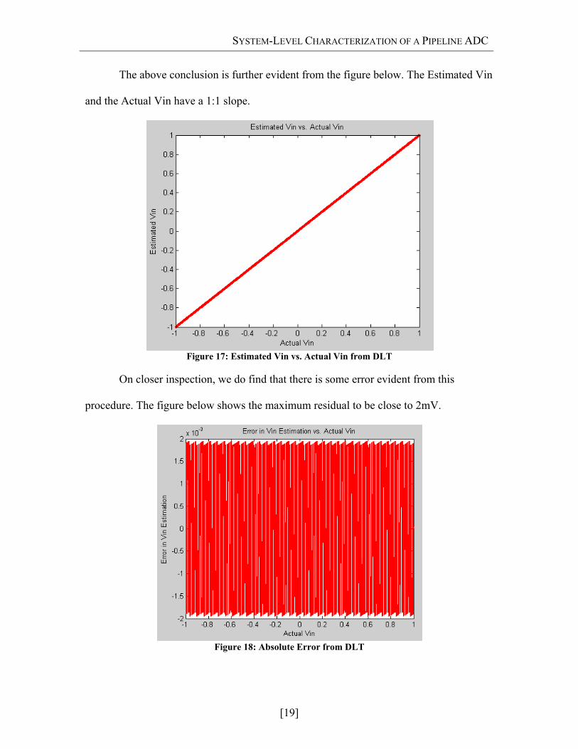
The above conclusion is further evident from the figure below. The Estimated Vin
and the Actual Vin have a 1:1 slope.
Figure 17: Estimated Vin vs. Actual Vin from DLT
On closer inspection, we do find that there is some error evident from this
procedure. The figure below shows the maximum residual to be close to 2mV.
Figure 18: Absolute Error from DLT

SYSTEM-LEVEL CHARACTERIZATION OF A PIPELINE ADC
[20]
This amount is far away from the max residual of 45.7µV we were looking to
implement. Further analysis and research on the DLT will be needed to verify the
feasibility of implementing such a procedure.

CIRCUIT-LEVEL SIMULATION OF THE ANALOG SUBSYSTEM
[21]
4. CircuitLevel Simulation of the Analog Subsystem The analog subsystem, which includes the Differential Pair, Common Mode
Feedback, Replica Bias, and the Switched Capacitor Network were simulated in Cadence.
This section explains the design of each of these blocks in detail. The stage1
implementation from [4] is repeated here for convenience:
Figure 19: Stage 1 Implementation of Pipeline ADC [4]
4.1. Basic Differential Pair Circuit The analog subsystem design began with the simulation of a resistively loaded
differential pair circuit. As explained in the Prior Work section, a resistive load was
preferred to an active load due to deep-submicron compatibility [4]. The low supply
voltage (2.5V and Ground) leaves little headroom for a load transistor causing it to easily
turn off. A resistively loaded approach means that the high-gain requirement of the diff-
pair should be relaxed and the non-linearity arising from this stage corrected digitally.
The differential pair circuit specifications were as follows:
• Differential Mode gain = 8
• Input Bias Voltage = 1.25V

CIRCUIT-LEVEL SIMULATION OF THE ANALOG SUBSYSTEM
[22]
• Input Voltage Swing = +/-1.5 V
• Output Bias Voltage = 2 V
• Output Voltage Swing = +/- 0.4 V
• Bias Current = 200uA
• Rail Voltages = 2.5V, Gnd
The gain requirement is not stringent, meaning that proximity of 8 is acceptable.
This is again a big advantage in terms of design because a precision amplifier will
increase analog complexity where as the present design with its continuous digital
background calibration will estimate and remove imprecision errors digitally.
The first simulation was that of a simple differential pair circuit. Please see
Appendix A2 for circuit parameters. The simulated diff-pair circuit is shown below:
Figure 20: Circuit Schematic of a Simple Diff-Pair

CIRCUIT-LEVEL SIMULATION OF THE ANALOG SUBSYSTEM
[23]
An important design choice was that of a reasonable gate overdrive voltage, VOV,
for the input transistors. A higher overdrive voltage increases the linear range of the
differential input; although any increase in VOV must be supported by a proportional
increase in tail current to maintain constant transconductance:
OV
biasm V
IG =
Constant transconductance is necessary because the differential pair gain is given by:
|Gain| = |-GmRD|
where RD is the load resistor value and the Gain is 8.
To find the optimal VOV, the diff-pair circuit shown above was simulated using 4
overdrive voltages: 150, 200, 250, and 300mV. In addition to comparing the plots of
differential output versus input, cubic approximations were fit to each of the 4 cases, to
compare the residue (difference between simulated data and fit). The results are shown
below:
Figure 21: Basic Diff-Pair Output Characteristics for 4 different Vov.
-0.3 -0.2 -0.1 0 0.1 0.2 0.3
-1.5
-1
-0.5
0
0.5
1
1.5
Vin1 - Vin2 [volts]
Vou
t1 -
Vou
t2 [v
olts
]
Differential Pair Gain of 8 - Superimposing all 4 overdrive voltage cases
150mV200mV250mV300mV

CIRCUIT-LEVEL SIMULATION OF THE ANALOG SUBSYSTEM
[24]
The general pattern that is evident from superimposing all 4 VOV cases is that the
linear range of the differential output increases with increasing VOV. The slope near the
operating point (i.e. differential gain) in all the cases is approximately 8 as expected
because the load resistor values were adjusted in each case to yield a gain of 8. However
the output bias voltage will naturally change with varying load resistor values because of
the varying voltage drop across the load. It is obvious then that only 1 of 3 diff-pair
specifications can be met with a basic diff-pair circuit:
• Differential Mode Gain
• Output Bias Voltage
• Output Voltage Swing
Achieving all 3 specifications would require a more complex design, which is
covered in the next section.
In terms of a cubic approximation for the differential output signal, the following
plots for differential output and residue were produced (input voltage steps of 0.001
Volts). Since the differential input is fed into a 4-bit Flash ADC (16 levels), and the input
signal swing is assumed to be +/- 1.5 V, there are 3/16 = 188mV in each code level.
Therefore the differential input range of +/- 94mV is of primary concern.
The following plots show the differential output and residue versus differential
input for all 4 VOV cases.

CIRCUIT-LEVEL SIMULATION OF THE ANALOG SUBSYSTEM
[25]
Figure 22: Residue Plot for an Overdrive Voltage of 150mV
Figure 23: Residue Plot for an Overdrive Voltage of 200mV

CIRCUIT-LEVEL SIMULATION OF THE ANALOG SUBSYSTEM
[26]
Figure 24: Residue Plot for an Overdrive Voltage of 250mV
Figure 25: Residue Plot for an Overdrive Voltage of 300mV

CIRCUIT-LEVEL SIMULATION OF THE ANALOG SUBSYSTEM
[27]
After comparing the Max of Residues in each case, the smallest residue occurs
with an overdrive voltage of 250mV. This implies that an overdrive voltage of 250mV is
the ideal choice, and digital correction of this non-linearity will further decrease the Max
Residue.
Table 2: Overdrive Voltage Residue Results Summary
Overdrive Voltage |Max of Residue| [µV]150 mV 125 200 mV 90 250 mV 70 300 mV 140
As mentioned earlier in the section, the need to simultaneously meet the
differential gain, output bias voltage and output voltage swing specifications requires the
use of an alternative design. In addition, a design that lowers the Max Residue for the
300mV OV case is investigated in the next section.

CIRCUIT-LEVEL SIMULATION OF THE ANALOG SUBSYSTEM
[28]
4.2. Cascode DiffPair with PiResistor Network As shown in the previous section, a design that controls differential gain, output
bias voltage and output swing independent of each other is desired. In addition, a design
that decreases the Max Residue for an overdrive voltage of 300mV below that of the 250
mV case would be useful.
The Basic Diff-Pair output versus input plot is repeated here for convenience:
Figure 26: Basic Diff-Pair Output versus Input for Various Overdrive Voltages
It is obvious that the 300mV curve has a different shape than the other three in the
differential input range of +/- 1V. A possible explanation was that changes in the diff-pair
output voltage causes the MOSFET VDS to vary, and therefore at overdrive voltages
greater than 250mV the transistor crashes into the triode region.
-1.5 -1 -0.5 0 0.5 1 1.5-2.5
-2
-1.5
-1
-0.5
0
0.5
1
1.5
2
2.5
Vin1 - Vin2 [volts]
Vou
t1 -
Vou
t2 [v
olts
]
Differential Pair Gain of 8 - Superimposing all 4 overdrive voltage cases
150mV200mV250mV300mV

CIRCUIT-LEVEL SIMULATION OF THE ANALOG SUBSYSTEM
[29]
To verify this hypothesis, a cascode gain stage was added to the diff-pair. A
cascode has two main properties:
1. High Output Impedance, resulting in high gain, and
2. Limiting the voltage across the input transistor
To illustrate the first property, a simple common source amplifier is simulated
with and without a cascode. As shown below, the non-cascode curve has a positive slope
in the active region, whereas the cascode has an almost zero slope. Since the output
impedance is given by the inverse of the slope, it is obvious that the cascode has
produced very high (ideally infinite) output impedance by removing the Gate-Drain
Capacitance (Miller Effect).
Figure 27: Illustration of Cascode High Output Impedance
0 0.5 1 1.5 2 2.50
1
2
3
4
5
6x 10⁻⁴
Vds[Volts]
Id[u
A]
Effect of Cascode
Simple CS AmplifierCascode Amplifier

CIRCUIT-LEVEL SIMULATION OF THE ANALOG SUBSYSTEM
[30]
Figure 28: Simple Common Source Circuit
Figure 29: Cascoded Common Source Circuit
The cascode was therefore implemented in the diff-pair design to see if the issue
with the 300mV curve is resolved. This configuration is referred to as a telescopic-
cascode.
The figures below show a comparison of a cascode diff-pair with a non-cascode
diff-pair in terms of differential output versus input characteristic, and differential gain.
Figure 30: Comparison of Cascode and Non-Cascode Diff-Pair Output Characteristics
-2.5 -2 -1.5 -1 -0.5 0 0.5 1 1.5 2 2.5-2.5
-2
-1.5
-1
-0.5
0
0.5
1
1.5
2
2.5
Vin1-Vin2[Volts]
Vou
t2-V
out1
[Vol
ts]
Differential Gain Comparison with Vov = 300mV
With CascodeWithout Cascode

CIRCUIT-LEVEL SIMULATION OF THE ANALOG SUBSYSTEM
[31]
Clearly, the addition of a cascode did very little to improve the shape of the curve.
However, the small-signal gain at the operating point did increase from 4.5 V/V to about
5.3 V/V. This graph is obtained by taking the first-derivative of the above curve.
In this simulation, the RD is set to 24K, and W = 1.23um.
Figure 31: Small Signal Gain Comparison of Cascode and Non-Cascode Diff-Pair
One possible explanation for this behavior is that in the small signal model, the
high output impedance of the cascode stage is placed in parallel with the resistive load of
the diff-pair. Therefore the maximum effective output resistance of the diff pair is
dominated by the resistive load. By increasing the resistive load, however, will lead to a
lower output bias voltage, and will cause the input MOSFETS to crash into triode.
To overcome this issue of gain versus output bias, a Pi-Resistor configuration is
used, which is basically a resistor that connects both the outputs. This extra resistor, RG,
-2.5 -2 -1.5 -1 -0.5 0 0.5 1 1.5 2 2.50
1
2
3
4
5
6
Vin1-Vin2[Volts]
Gai
n[V
/V]
Differential Gain Comparison with Vov = 300mV
With CascodeWithout Cascode

CIRCUIT-LEVEL SIMULATION OF THE ANALOG SUBSYSTEM
[32]
reduces the gain because in differential mode RG/2 is placed in parallel with the load
resistor, RB. Nevertheless in common mode RG is Open, and only RB controls the output
bias voltage. As a result RB is picked to be a large enough resistor, i.e.
RB || RG/2 > RD
where RD is Gain/Transconductance. RG, which is used to knock down the gain to a
desired level, is then picked accordingly to satisfy the above equation.
Figure 32: Cascode Diff-Pair with Pi-Resistor Network

CIRCUIT-LEVEL SIMULATION OF THE ANALOG SUBSYSTEM
[33]
Table 3: Summary of Cascode Diff-Pair Parameters
VOV [mV] W [um] for
M1, M2 W [um] for
N6, N7
Load Resistance
[KΩ]
R7 [K Ohms]
Gm [µA/V]
150 4.91 4.91 12 96 6.666 * 10-3 200 2.76 4.91 16 120 5 * 10-3 250 1.77 4.91 20 100000 4 * 10-3
The differential output versus input for the above circuit is shown below, along
with residue plot for the 250mV case.
Figure 33: Cascoded Diff-Pair Differential Output versus Input characteristic
-0.3 -0.2 -0.1 0 0.1 0.2 0.3-2
-1.5
-1
-0.5
0
0.5
1
1.5
2
Vin1-Vin2[Volts]
Vou
t2-V
out1
[Vol
ts]
Differential Gain with Resistor Network, and Cascode
150mV200mV250mV

CIRCUIT-LEVEL SIMULATION OF THE ANALOG SUBSYSTEM
[34]
Figure 34: Cascoded Diff-Pair Residue Plot
A quick comparison of the first plot with that of the non-cascoded diff-pair shows
that both the differential gain and output bias voltage specifications can be met using this
design. The second plot shows that the use of a cascode did very little, if any, to improve
the Maximum Residue Voltage. These two results are as expected because the resistor
network allows the independent control of both output bias voltage and the gain, and the
cascode is meant to increase output impedance.
In any case, the differential voltage swing specification is still not met because it
depends on the current through each input transistor and the load resistance, both of
which are fixed in this design:
Voltage swing = 0.4 = ID * RD
Choosing RD from the above equation is not an option since the gain has to be fixed at 8:

CIRCUIT-LEVEL SIMULATION OF THE ANALOG SUBSYSTEM
[35]
RD = Gain / Gm
= 8 / 800μA/V
= 10KΩ.
(Gm = 2*ID / VOV , where ID = IBIAS / 2= 100μA and VOV = 0.25V)
Changing ID would change the transconductance of the input transistors that will
once again affect the diff-pair gain:
Gm = ⎟⎠⎞
⎜⎝⎛
LWCoxI nDμ2
In addition, an increase in ID will increase the voltage drop across the load
resistors, and will bring down the output bias voltage causing the MOSFETs to crash.
Therefore, ID needed to be changed in a way that satisfies the Voltage Swing condition
but keeps the output bias at 2V and the input MOSFET transconductance at 800μA/V.
The “Split Current” approach solves this issue by only providing a fraction of the
bias current through the load resistor. The current then through each load resistor is
BIASIx *)21( − where x is chosen such that the output bias voltage spec is satisfied. The
remaining current is provided directly to the drain of the input MOSFET when the
common mode control is implemented. This satisfies the input MOSFET
transconductance specification. The parameters and values chosen for the Cascoded Diff-
Pair are detailed in Appendix A3.

CIRCUIT-LEVEL SIMULATION OF THE ANALOG SUBSYSTEM
[36]
4.3. Common Mode Feedback & Replica Bias Due to the enhanced output resistance, the output biasing point is unstable and
highly sensitive to supply voltage variations and complementary device mismatches. It
results in dc biasing deviation and unwanted ac coupling [5]. To overcome this drawback,
common-mode feedback is used for bias stabilization and a Replica-Tail Feedback
technique to keep the tail current constant despite variations in the input common mode
voltage level [6].
The Common Mode Feedback (CMFB) works by sensing the output common
mode voltage, VOCM, and comparing it to a reference voltage of 2V. When VOCM = 2V,
the default 60μA is sent to the drain of the input transistor (refer to Appendix A3 for
explanation of this 60μA). If VOCM increases, the CMFB current is reduced accordingly to
bring VOCM back to 2V. Similarly, a decrease in VOCM will cause the CMFB to pump
additional current to bring VOCM back to 2V. This circuit works in a negative feedback
loop, pumping additional or less current depending on the common mode voltage.
As shown in the circuit on the next page, an actively loaded diff-pair senses the
common mode output. The output of this sensing circuit is connected to 2 PMOS
transistors which route the current back to the cascoded diff-pair in a feedback loop.
The Replica Bias technique is needed to reduce overall sensitivity to ambient
temperature changes. As temperature increases, the load resistance increases, causing the
gain to increase unpredictably. To minimize this possibility, the replica bias circuit
adjusts the bias current as necessary by sensing the input and output voltages. The replica
bias transistors are scaled down by a factor of 8 compared to the input MOSFETs to

CIRCUIT-LEVEL SIMULATION OF THE ANALOG SUBSYSTEM
[37]
reduce power consumption. Appendix A3 lists all the circuit parameters of the figure
below.
Figure 35: Circuit Schematic of Cascoded Diff-Pair with CMFB and Replica Bias

CIRCUIT-LEVEL SIMULATION OF THE ANALOG SUBSYSTEM
[38]
Figure 36: Bias Circuit for Diff-Pair and CMFB

CIRCUIT-LEVEL SIMULATION OF THE ANALOG SUBSYSTEM
[39]
The voltage output versus differential input plot is shown below. As expected, the
output bias voltage is fixed at 2V, the output swing is +/- 0.4V, and the actual gain is
approximately 6.1.
Figure 37: Output vs. Input for Cascode Diff-Pair with CMFB and Replica Bias
Since the +/- 94 mV range is of primary concern, the differential output versus
differential input plot on the next page shows the behavior in that range.
-0.2 -0.15 -0.1 -0.05 0 0.05 0.1 0.15 0.21.5
1.6
1.7
1.8
1.9
2
2.1
2.2
2.3
2.4
2.5
Vin1-Vin2[Volts]
Out
put V
olta
ges
[Vol
ts]
Voltage Output versus Differential Input for Diff-Pair with CMFB & Replica Bias
Vout1Vout2

CIRCUIT-LEVEL SIMULATION OF THE ANALOG SUBSYSTEM
[40]
Figure 38: Differential Output versus Differential Input for Cascode Diff-Pair with CMFB
Figure 39: Operating point gain for a Cascode Diff-Pair with CMFB & Replica Bias
-0.1 -0.08 -0.06 -0.04 -0.02 0 0.02 0.04 0.06 0.08 0.1-0.8
-0.6
-0.4
-0.2
0
0.2
0.4
0.6
0.8
Vin1-Vin2[Volts]
Vou
t2-V
out1
[Vol
ts]
Differential Output versus Differential Input for Diff-Pair with CMFB & Replica Bias
-0.1 -0.08 -0.06 -0.04 -0.02 0 0.02 0.04 0.06 0.08 0.15.5
5.6
5.7
5.8
5.9
6
6.1
6.2
6.3
Vin1-Vin2[Volts]
Gai
n[V
/V]
Differential Mode Gain for Diff-Pair with CMFB & Replica Bias

CIRCUIT-LEVEL SIMULATION OF THE ANALOG SUBSYSTEM
[41]
4.4. DiffPair Settling time
Figure 40: Test Circuit for Measuring Settling Time of Diff-Pair

CIRCUIT-LEVEL SIMULATION OF THE ANALOG SUBSYSTEM
[42]
Figure 41: Setting Time Performance Input and Output Voltage
The input voltages are 2 square waves with 1us period and a 1.2V – 1.3V pk-pk.
Vin1 has a +500mV AC signal riding on a 1.25DC bias and Vin2 has a -500mV AC
signal riding on the same bias voltage. The maximum and minimum output voltages can
be predicted by grounding one input terminal of the diff-pair and forcing all the current to
flow through the other half of the diff-pair. This resulted in a maximum Vout of
2.241348V, and a minimum Vout of 1.771552V.
For a 14-bit ADC, the first 11bits are of high importance to us, and therefore
settling time is measured primarily for those 11bits. Therefore, (0.8)/(211) = 390µV. As a
result the settling performance is characterized by the time it takes for the amplifier to
settle within +/- 390 µV of the maximum and minimum output voltages. This means
2.241348V - 390µV = 2.240958V, and 1.771162+390µV = 1.771552V are the voltage

CIRCUIT-LEVEL SIMULATION OF THE ANALOG SUBSYSTEM
[43]
levels at which the settling time should be measured. Doing so results in a rise-time of
64ns and a fall-time of 62.35ns.
Figure 42: Rise-Time Measurement
Figure 43: Fall-Time Measurement

CIRCUIT-LEVEL SIMULATION OF THE ANALOG SUBSYSTEM
[44]
The step size was 1*10-12 and the max step was 1 * 10 -8
Figure 44: AC Simulation of Differential Pair
The AC simulation of the Differential pair with 1pF load capacitors across the
outputs, and another 1pF capacitor between the Gm stage and the CMFB. The 3dB
frequency bandwidth = 16.1 MHz, which is comparable to the value obtained through the
DC simulations (11 MHz). :

CIRCUIT-LEVEL SIMULATION OF THE ANALOG SUBSYSTEM
[45]
4.5. Switched Capacitor Network Switched-capacitor networks have become very popular due to their accurate
frequency response as well as good linearity and dynamic range. Filter coefficients of a
switched capacitor network can be easily obtained as they are determined by capacitance
ratios which can be set very precisely on an integrated circuit (with an order of 0.1
percent error). By modifying the capacitance ratios, we can change the settling time and
also the frequency response of the entire network. Moreover, a switched-capacitor
network takes up a dramatically less amount of die-area as compared to a simple RC
integrator, which may serve the same purpose. A smaller amount of die-area also results
in a lower cost as size is very costly in IC manufacturing industry.
The schematic of our initial block is shown below. This circuit has two main
phases. In phase 1 (P1), the capacitor is sampling the input voltage relative to 1.25V. In
phase 2 (P2), the potential to the left and to the right of capacitor adjust to correct for the
DAC voltage levels. Although complicated, this process occurs systematically. At any
given time, either P1 or P2 signals are turned high but never at the same time. If they
happen to be turned on at the same time, then charges get lost and are transferred from
one MOSFET to another incorrectly and hence the correct voltage cannot be sampled.

CIRCUIT-LEVEL SIMULATION OF THE ANALOG SUBSYSTEM
[46]
Figure 45: Switched-Capacitor Network Schematic

CIRCUIT-LEVEL SIMULATION OF THE ANALOG SUBSYSTEM
[47]
When P1 is high, the potential to the right of the capacitor, O2, is set to a constant
1.25V. The potential to the left of the capacitor, O1, is set to the input voltage of the
Sample and Hold Circuit. This separation of charge between the capacitor plates charges
up the capacitor, and hence the capacitor samples the input voltage relative to the 1.25V
being supplied. When the capacitor has charged up to the correct voltage, then P1 turns
off and P2 turns on. At Phase 2, the voltage at the capacitor switches to the correct DAC
voltage level (0V, 1.25V or 2.5V) as determined by the DAC. There are two signals from
the DAC that indicate whether a signal is closer to a low, mid or high voltage. The truth
table of this is shown below.
Table 4: Truth Table for DAC Signals
DACP DACM On Signal Level 1 0 P2DPB High 0 0 P2DZ Mid 0 1 P2DM Low
When P2 is on and the DAC signals that a high voltage was detected for the input
voltage, then signal P2DPB turns off turning on the PMOS that it is connected to.
Turning on this MOSFET drives the voltage at the capacitor to the 2.5V rail. On the other
hand, if the DAC signals had indicated a mid voltage level, the P2DZ would have turned
on, and hence turned on the NMOS that it is connected to. Turning on this NMOS drives
the voltage at the capacitor to the 1.25V rail. Similarly if the DAC had signaled a low
voltage signal, then it would have turned on P2DM and hence turned on the NMOS
device that it is connected to. This would drive the voltage at the capacitor to the 0V rail.
In any of these three situations, the voltage difference between the sampling stage and the
DAC correction stage at O1 is reflected at O2 as well, as the capacitor tries to maintain
the same charge between its plates. Hence if Vin was 1.2V, and the DAC signaled this

CIRCUIT-LEVEL SIMULATION OF THE ANALOG SUBSYSTEM
[48]
voltage to be a midlevel voltage, then during the DAC correction stage, the voltage at the
capacitor would drive up to 1.25V. This change of 0.05V at O1 is shown at O2 as well
and hence drive the output voltage at O2 from 1.25V to 1.30V, keeping the charge of the
capacitor constant.
The signals for the master clock were designed using the logic shown in the
schematic shown on the next page.

CIRCUIT-LEVEL SIMULATION OF THE ANALOG SUBSYSTEM
[49]
Figure 46: Clock Signals for SCN

CIRCUIT-LEVEL SIMULATION OF THE ANALOG SUBSYSTEM
[50]
Transient analysis of the switch capacitor was done and the following results were
obtained. Our results support the theory that was explained above.
Figure 47: Transient Analysis of SCN

CIRCUIT-LEVEL SIMULATION OF THE ANALOG SUBSYSTEM
[51]
The schematic with the Switched capacitor and Diff-pair connected together is
shown below.
Figure 48: Schematic of Switched Capacitor Network and Diff-pair together

CIRCUIT-LEVEL SIMULATION OF THE ANALOG SUBSYSTEM
[52]
Further transient analysis was conducted on this new circuit, which resulted in the
following results.
Figure 49: Transient Analysis of Switched Capacitor Network and Diff-pair together
More analysis will need to be done to measure the settling times of this process.
This may result in the tweaking of the design and the adjustment of certain component
values.

QUANTIZER
[53]
5. Quantizer The design of the pipeline ADC consists of a 4-bit quantizer. The following
circuit is a 2-bit quantizer designed by Tsai Chen, and we are in the process of modifying
it to 4-bit. In this design the voltage reference levels are set by mismatches in the current
sources. However, a main concern with that design is the 100K resistor in the preamp,
which slows down the circuit.
Figure 50: Preamp for the Quantizer
An alternative approach that was implemented in a 3-bit pipeline ADC by
Thomas Liechti uses a differential difference amplifier with a 2 Vpp differential signal
(1Vpp single ended) and centered about Vdd/2 (=0.9V).

work
The volta
k for our desi
Figur
age levels are
ign.
re 51: Alternat
e generated
[54]
tive Approach
using a resi
h for Quantize
stive ladder,
er
, and this ap
QUANTIZER
pproach coul
R
ld

CONCLUSION
[55]
6. Conclusion This project has made significant progress in our aim to design a 16-bit 10Mhz
Pipeline ADC. We have successfully been able to:
• characterize the System-level functionality of a Pipeline ADC by simulating its
features using Matlab and
• design the majority of the analog subsystem of the ADC in Cadence.
The simulation work has corroborated our theory and helped analyze our design
block. It has provided us an opportunity to compare and contrast the ideal and non ideal
behavior of an ADC.
Due to the complexity of the project and the various hurdles we came upon during
the design phase, we did not have enough time to be able to achieve all the goals we set
out to meet initially. Some of the work that still needs to be completed includes the
fabrication work including the lay out work of the analog subsystem. Once the fabricated
IC has been received, further work will be needed for data acquisition using a software
package similar to LabView. Further transient analysis may need to be completed on the
final design block to verify its performance. Moreover, work will also need to be done on
the FPGA for designing the background calibration.

REFERENCES
[56]
7. References [1] J. McNeill, M.Coln, and B.Larivee, ““Split ADC” architecture for deterministic
digital background calibration of a 16b 1MS/s ADC,” IEEE J. Solid State Circuits, Vol.40, No.12, December 2005.
[2] D.G. Morrison, “Basics of Design: Analog to Digital Converters”, Electronic
Design, October 13, 2003 [3] D.A. Johns and K.Martin, “Analog Integrated Circuit Design”, John Wiley, 2002,
pp. 487. [4] B.Murmann and B. Boser, “A 12-bit 75-MS/s Pipelined ADC Using Open-Loop
Residue Amplification”, IEEE J. Solid State Circuits, Vol.38, No.12, December 2003.
[5] G.N. Lu and G.Sou, “A CMOS Low-Voltage, High-Gain Op-Amp”, IEEE
Proceedings of the 1997 European Design and Test Conference, 1997. [6] K.Gulati and H-S.Lee, “A high-swing CMOS telescopic Operational amplifier”,
IEEE J. Solid State Circuits, Vol.33, pp. 2010-2019, Dec 1998.

APPENDIX A: MATLAB CODE
[57]
Appendix A: Matlab Code I. Simulating a linear multistage ADC
% simulated Vin Vin(1,:) = 2.*(rand(1,10000)-0.5); % code edges of each level edges = [-1.4063, -1.2188, -1.0313, -0.8438, -0.6563, -0.4688, -0.2813,
-0.0938, 0.0938, 0.2813, 0.4688, 0.6563, 0.8438, 1.0313, 1.2188, 1.4063];
% # of stages in the ADC Stages = 3; % Analog Gain (amplification factor of error) AGain = 6.1; % Digital Gain (reconstruction) DGain = 1.00 * AGain; % Reference Voltage Vref = 1.5; for j = 1:Stages % Setting the lowest level to -8 Nout(j,:) = zeros(size(Vin(j,:)))-8; for i = 1:length(edges)
% compare each value of Vin to the code edges
I = find ( Vin(j,:) >= edges(i) ); % set the Nout value for each Vin
Nout(j,I) = i-8; end % calculates the error from a stage (residue) Verr(j,:) = Vin(j,:) - Nout(j,:)*(Vref/8); % calculates the input voltage for the next stage ADC by amplifying % the error from the previous stage with some nonlinearity factor Vin(j+1,:) = AGain .* Verr(j,:); end

APPENDIX A: MATLAB CODE
[58]
II. Estimating Vin and ADC error from each stage %% CALCULATING ESTIMATED VIN AND ADC ERROR OF EACH STAGE for j = 1:Stages % estimate Vin for the first stage of the ADC if (j == 1) Vinest(j,:) = Vref*(Nout(j,:)/8); else
% estimate Vin for the other stages of the ADC Vinest(j,:) = Vinest(j-1,:) + Vref*(Nout(j,:)/(8*DGain^(j-1))); end error(j,:) = Vinest(j,:)-Vin(1,:); end

APPENDIX A: MATLAB CODE
[59]
III. Simulating a nonlinear multi stage ADC % simulated Vin Vin(1,:) = 2.*(rand(1,10000)-0.5); % code edges of each level edges = [-1.4063, -1.2188, -1.0313, -0.8438, -0.6563, -0.4688, -0.2813,
-0.0938, 0.0938, 0.2813, 0.4688, 0.6563, 0.8438, 1.0313, 1.2188, 1.4063];
% # of stages in the ADC Stages = 3; % Analog Gain (amplification factor of error) AGain = 6.1; % Digital Gain (reconstruction) DGain = 1.00 * AGain; % Reference Voltage Vref = 1.5; % Non-Linearity Factor Vnonlinfactor = 3 * Vref; for j = 1:Stages % Setting the lowest level to -8 Nout(j,:) = zeros(size(Vin(j,:)))-8; for i = 1:length(edges)
% compare each value of Vin to the code edges
I = find ( Vin(j,:) >= edges(i) ); % set the Nout value for each Vin
Nout(j,I) = i-8; end % calculates the error from a stage (residue) Verr(j,:) = Vin(j,:) - Nout(j,:)*(Vref/8); % calculates the input voltage for the next stage ADC by amplifying % the error from the previous stage with some nonlinearity factor Vin(j+1,:) = AGain .* Verr(j,:).*(1-(Verr(j,:).*Vnonlinfactor).^2); end

APPENDIX A: MATLAB CODE
[60]
IV. Simulated data from Cadence showing nonlinearity % simulated Vin Vin(1,:) = 2.*(rand(1,10000)-0.5); % simulated data imported from cadence for a 250mV overdrive Gain250I=Gain250InputRange94mV20KDataPoints'; % code edges of each level edges = [-1.4063, -1.2188, -1.0313, -0.8438, -0.6563, -0.4688, -0.2813,
-0.0938, 0.0938, 0.2813, 0.4688, 0.6563, 0.8438, 1.0313, 1.2188, 1.4063];
% # of stages in the ADC Stages = 3; % Analog Gain (amplification factor of error) AGain = 6.1; % Digital Gain (reconstruction) DGain = 1.00 * AGain; % Reference Voltage Vref = 1.5; for j = 1:Stages % Setting the lowest level to -8 Nout(j,:) = zeros(size(Vin(j,:)))-8; for i = 1:length(edges)
% compare each value of Vin to the code edges
I = find ( Vin(j,:) >= edges(i) ); % set the Nout value for each Vin
Nout(j,I) = i-8; end % calculates the error from a stage (residue) Verr(j,:) = Vin(j,:) - Nout(j,:)*(Vref/8); % calculates the input voltage for the next stage ADC by amplifying % the error from the previous stage with the nonlinearity factor % from cadence simulated data for k = 1:length(Verr(j,:)) location = length(find(Gain250I(1,:)<=Verr(j,k)))+1; Vin(j+1,k)=Gain250I(2,location); end end

APPENDIX A: MATLAB CODE
[61]
V. Correcting nonlinearity of a simulated multistage ADC % simulated Vin Vin(1,:) = 2.*(rand(1,10000)-0.5); % code edges of each level edges = [-1.4063, -1.2188, -1.0313, -0.8438, -0.6563, -0.4688, -0.2813,
-0.0938, 0.0938, 0.2813, 0.4688, 0.6563, 0.8438, 1.0313, 1.2188, 1.4063];
% # of stages in the ADC Stages = 3; % Analog Gain (amplification factor of error) AGain = 6.1; % Digital Gain (reconstruction) DGain = 1.00 * AGain; % Reference Voltage Vref = 1.5; % Non-Linearity Factor Vnonlinfactor = 3 * Vref; for j = 1:Stages % Setting the lowest level to -8 Nout(j,:) = zeros(size(Vin(j,:)))-8; for i = 1:length(edges)
% compare each value of Vin to the code edges
I = find ( Vin(j,:) >= edges(i) ); % set the Nout value for each Vin
Nout(j,I) = i-8; end % calculates the error from a stage (residue) Verr(j,:) = Vin(j,:) - Nout(j,:)*(Vref/8); % calculates the input voltage for the next stage ADC by amplifying % the error from the previous stage with some nonlinearity factor Vin(j+1,:) = AGain .* Verr(j,:).*(1-(Verr(j,:).*Vnonlinfactor).^2); % NON-LINEARITY CORRECTION FROM CUBIC APPROXIMATION coeff = polyfit(Vres(j,:),Vin(j+1,:),3);
cubic(j,:) = coeff(1)*Vres(j,:).^3 +
coeff(2)*Vres(j,:).^2 + coeff(3)*Vres(j,:)+ coeff(4);
Vin(j+1,:) = Vin(j+1,:)./cubic(j,:).*DGain.*Vres(j,:) ; end

APPENDIX A: MATLAB CODE
[62]
VI. Correcting nonlinearity of simulated data from Cadence % simulated Vin Vin(1,:) = 2.*(rand(1,10000)-0.5); % simulated data imported from cadence for a 250mV overdrive Gain250I=Gain250InputRange94mV20KDataPoints'; % code edges of each level edges = [-1.4063, -1.2188, -1.0313, -0.8438, -0.6563, -0.4688, -0.2813,
-0.0938, 0.0938, 0.2813, 0.4688, 0.6563, 0.8438, 1.0313, 1.2188, 1.4063];
% # of stages in the ADC Stages = 3; % Analog Gain (amplification factor of error) AGain = 6.1; % Digital Gain (reconstruction) DGain = 1.00 * AGain; % Reference Voltage Vref = 1.5; for j = 1:Stages % Setting the lowest level to -8 Nout(j,:) = zeros(size(Vin(j,:)))-8; for i = 1:length(edges)
% compare each value of Vin to the code edges
I = find ( Vin(j,:) >= edges(i) ); % set the Nout value for each Vin
Nout(j,I) = i-8; end % calculates the error from a stage (residue) Verr(j,:) = Vin(j,:) - Nout(j,:)*(Vref/8); % calculates the input voltage for the next stage ADC by amplifying % the error from the previous stage with the nonlinearity factor % from cadence simulated data for k = 1:length(Verr(j,:)) location = length(find(Gain250I(1,:)<=Verr(j,k)))+1; Vin(j+1,k)=Gain250I(2,location); end % NON-LINEARITY CORRECTION FROM CUBIC APPROXIMATION coeff = polyfit(Vres(j,:),Vin(j+1,:),3);
cubic(j,:) = coeff(1)*Vres(j,:).^3 +
coeff(2)*Vres(j,:).^2 +

APPENDIX A: MATLAB CODE
[63]
coeff(3)*Vres(j,:)+ coeff(4);
Vin(j+1,:) = Vin(j+1,:)./cubic(j,:).*DGain.*Vres(j,:) ; end

APPENDIX A: MATLAB CODE
[64]
VII. Simulating the basics of a SplitADC architecture % input voltage to Pipeline ADC A & B VinA(1,:) = -1.5:0.0001:1.5; VinB(1,:) = VinA(1,:); % code edges for ADC A edgesA(1:5,:) = [-1.4063, -1.2188, -1.0313, -0.8438, -0.6563, -0.4688,
-0.2813, -0.0938, 0.0938, 0.2813, 0.4688, 0.6563, 0.8438, 1.0313, 1.2188, 1.4063;
-1.4063, -1.2188, -1.0313, -0.8438, -0.6563, -0.4688, -0.2813, -0.0938, 0.0938, 0.2813, 0.4688, 0.6563, 0.8438, 1.0313, 1.2188, 1.4063;
-1.4063, -1.2188, -1.0313, -0.8438, -0.6563, -0.4688, -0.2813, -0.0938, 0.0938, 0.2813, 0.4688, 0.6563, 0.8438, 1.0313, 1.2188, 1.4063;
-1.4063, -1.2188, -1.0313, -0.8438, -0.6563, -0.4688, -0.2813, -0.0938, 0.0938, 0.2813, 0.4688, 0.6563, 0.8438, 1.0313, 1.2188, 1.4063;
-1.4063, -1.2188, -1.0313, -0.8438, -0.6563, -0.4688, -0.2813, -0.0938, 0.0938, 0.2813, 0.4688, 0.6563, 0.8438, 1.0313, 1.2188, 1.4063];
% code edges for ADC B edgesB(1:5,:) = [-1.4063, -1.2188, -1.0313, -0.8438, -0.6563, -0.4688,
-0.2813, -0.0938, 0.0938, 0.2813, 0.4688, 0.6563, 0.8438, 1.0313, 1.2188, 1.4063;
-1.4063, -1.2188, -1.0313, -0.8438, -0.6563, -0.4688, -0.2813, -0.0938, 0.0938, 0.2813, 0.4688, 0.6563, 0.8438, 1.0313, 1.2188, 1.4063;
-1.4063, -1.2188, -1.0313, -0.8438, -0.6563, -0.4688, -0.2813, -0.0938, 0.0938, 0.2813, 0.4688, 0.6563, 0.8438, 1.0313, 1.2188, 1.4063;
-1.4063, -1.2188, -1.0313, -0.8438, -0.6563, -0.4688, -0.2813, -0.0938, 0.0938, 0.2813, 0.4688, 0.6563, 0.8438, 1.0313, 1.2188, 1.4063;
-1.4063, -1.2188, -1.0313, -0.8438, -0.6563, -0.4688, -0.2813, -0.0938, 0.0938, 0.2813, 0.4688, 0.6563, 0.8438, 1.0313, 1.2188, 1.4063];
%Above edges are ideal - but because of redundancy we should be able to %handle edges higer or lower. Bump up, down by 1/4 LSB edgesA(1,:) = edgesA(1,:) - .1875/4; edgesB(1,:) = edgesB(1,:) + .1875/4; % # of stages in the ADC Stages = 5; % ADC A Parameters % Analog Gain (amplification factor of error) AGainA = [6.5, 6.5, 6.5, 6.5, 6.5]; % Digital Gain (reconstruction) DGainA = 1.00 * AGainA;

APPENDIX A: MATLAB CODE
[65]
% Reference Voltage VrefA = 1.5; % Non-Linearity Factor AlphaA = [10.0 * VrefA, 0 * VrefA, 0 * VrefA, 0 * VrefA, 0 * VrefA]; weightsA = [ 1 ; 1/(AGainA(1)) ; 1/(AGainA(1)*AGainA(2)) ; 1/(AGainA(1)*AGainA(2)*AGainA(3)) ; 1/(AGainA(1)*AGainA(2)*AGainA(3)*AGainA(4)) ]'; subweightsA = AGainA(1)*weightsA(2:5); % ADC B Parameters AGainB = [6.5, 6.5, 6.5, 6.5, 6.5]; DGainB = 1.00 * AGainB; VrefB = 1.5; AlphaB = [10.0 * VrefA, 0 * VrefA, 0 * VrefA, 0 * VrefA, 0 * VrefA]; weightsB = [ 1 ; 1/(AGainB(1)) ; 1/(AGainB(1)*AGainB(2)) ; 1/(AGainB(1)*AGainB(2)*AGainB(3)) ; 1/(AGainB(1)*AGainB(2)*AGainB(3)*AGainB(4)) ]'; subweightsB = AGainB(1)*weightsB(2:5); % Decisions NoutA, NoutB come from this part for j = 1:Stages % setting the lowest code level of ADC A to -8 NoutA(j,:) = zeros(size(VinA(j,:)))-8; % same as above for ADC B NoutB(j,:) = zeros(size(VinB(j,:)))-8; for i = 1:length(edgesA) % compare each value of Vin to the code edges for ADC A I = find ( VinA(j,:) >= edgesA(j,i) ); % set the output code value for each Vin NoutA(j,I) = i-8; end % same as above for ADC B for i = 1:length(edgesB) I = find ( VinB(j,:) >= edgesB(j,i) ); NoutB(j,I) = i-8; end % Previous makes -8 < N < 8 % Fix so they go from -1 to 1 NoutA(j,:) = (1/8)*NoutA(j,:); NoutB(j,:) = (1/8)*NoutB(j,:);

APPENDIX A: MATLAB CODE
[66]
% Following is the DAC subtract function % calculates the error of a stage for ADC A VerrA(j,:) = VinA(j,:) - NoutA(j,:)*(VrefA); % same as above for ADC B VerrB(j,:) = VinB(j,:) - NoutB(j,:)*(VrefB); % Then do gain and nonlinearity
% calculate input voltage for the next stage of ADC A by amplifying % the error from the previous stage with some nonlinearity factor
VinA(j+1,:)= AGainA(j).*VerrA(j,:).*(1-(VerrA(j,:).*AlphaA(j)).^2); % same as above for ADC B VinB(j+1,:)= AGainB(j).*VerrB(j,:).*(1-(VerrB(j,:).*AlphaB(j)).^2); end % Turn decisions into CODES % find the total code output for ADC A CODESA = weightsA*NoutA; % find the total code output for ADC B CODESB = weightsB*NoutB; % Split ADC Process - Average the two output codes! CODES = (CODESA + CODESB)/2; % Above are uncorrected for nonlinearity % Nonlinearity correction needs "subCODES" which are 1st stage residues % as measured by remaining stages of ADC subCODESA = subweightsA*NoutA(2:5,:); subCODESB = subweightsB*NoutB(2:5,:);

APPENDIX A: MATLAB CODE
[67]
VIII. Simulating nonlinearity from Cadence using SplitADC architecture
% input voltage to Pipeline ADC A & B VinA(1,:) = -1.5:0.0001:1.5; VinB(1,:) = VinA(1,:); % imported data from cadence Gain250I=Gain250'; % code edges for ADC A edgesA(1:5,:) = [-1.4063, -1.2188, -1.0313, -0.8438, -0.6563, -0.4688,
-0.2813, -0.0938, 0.0938, 0.2813, 0.4688, 0.6563, 0.8438, 1.0313, 1.2188, 1.4063;
-1.4063, -1.2188, -1.0313, -0.8438, -0.6563, -0.4688, -0.2813, -0.0938, 0.0938, 0.2813, 0.4688, 0.6563, 0.8438, 1.0313, 1.2188, 1.4063;
-1.4063, -1.2188, -1.0313, -0.8438, -0.6563, -0.4688, -0.2813, -0.0938, 0.0938, 0.2813, 0.4688, 0.6563, 0.8438, 1.0313, 1.2188, 1.4063;
-1.4063, -1.2188, -1.0313, -0.8438, -0.6563, -0.4688, -0.2813, -0.0938, 0.0938, 0.2813, 0.4688, 0.6563, 0.8438, 1.0313, 1.2188, 1.4063;
-1.4063, -1.2188, -1.0313, -0.8438, -0.6563, -0.4688, -0.2813, -0.0938, 0.0938, 0.2813, 0.4688, 0.6563, 0.8438, 1.0313, 1.2188, 1.4063];
% code edges for ADC B edgesB(1:5,:) = [-1.4063, -1.2188, -1.0313, -0.8438, -0.6563, -0.4688,
-0.2813, -0.0938, 0.0938, 0.2813, 0.4688, 0.6563, 0.8438, 1.0313, 1.2188, 1.4063;
-1.4063, -1.2188, -1.0313, -0.8438, -0.6563, -0.4688, -0.2813, -0.0938, 0.0938, 0.2813, 0.4688, 0.6563, 0.8438, 1.0313, 1.2188, 1.4063;
-1.4063, -1.2188, -1.0313, -0.8438, -0.6563, -0.4688, -0.2813, -0.0938, 0.0938, 0.2813, 0.4688, 0.6563, 0.8438, 1.0313, 1.2188, 1.4063;
-1.4063, -1.2188, -1.0313, -0.8438, -0.6563, -0.4688, -0.2813, -0.0938, 0.0938, 0.2813, 0.4688, 0.6563, 0.8438, 1.0313, 1.2188, 1.4063;
-1.4063, -1.2188, -1.0313, -0.8438, -0.6563, -0.4688, -0.2813, -0.0938, 0.0938, 0.2813, 0.4688, 0.6563, 0.8438, 1.0313, 1.2188, 1.4063];
%Above edges are ideal - but because of redundancy we should be able to %handle edges higer or lower. Bump up, down by 1/4 LSB edgesA(1,:) = edgesA(1,:) - .1875/4; edgesB(1,:) = edgesB(1,:) + .1875/4; % # of stages in the ADC Stages = 5;

APPENDIX A: MATLAB CODE
[68]
% ADC A Parameters % Analog Gain (amplification factor of error) AGainA = [6.5, 6.5, 6.5, 6.5, 6.5]; % Digital Gain (reconstruction) DGainA = 1.00 * AGainA; % Reference Voltage VrefA = 1.5; % Non-Linearity Factor AlphaA = [10.0 * VrefA, 0 * VrefA, 0 * VrefA, 0 * VrefA, 0 * VrefA]; weightsA = [ 1 ; 1/(AGainA(1)) ; 1/(AGainA(1)*AGainA(2)) ; 1/(AGainA(1)*AGainA(2)*AGainA(3)) ; 1/(AGainA(1)*AGainA(2)*AGainA(3)*AGainA(4)) ]'; subweightsA = AGainA(1)*weightsA(2:5); % ADC B Parameters AGainB = [6.5, 6.5, 6.5, 6.5, 6.5]; DGainB = 1.00 * AGainB; VrefB = 1.5; AlphaB = [10.0 * VrefA, 0 * VrefA, 0 * VrefA, 0 * VrefA, 0 * VrefA]; weightsB = [ 1 ; 1/(AGainB(1)) ; 1/(AGainB(1)*AGainB(2)) ; 1/(AGainB(1)*AGainB(2)*AGainB(3)) ; 1/(AGainB(1)*AGainB(2)*AGainB(3)*AGainB(4)) ]'; subweightsB = AGainB(1)*weightsB(2:5); % Decisions NoutA, NoutB come from this part for j = 1:Stages % setting the lowest code level of ADC A to -8 NoutA(j,:) = zeros(size(VinA(j,:)))-8; % same as above for ADC B NoutB(j,:) = zeros(size(VinB(j,:)))-8; for i = 1:length(edgesA) % compare each value of Vin to the code edges for ADC A I = find ( VinA(j,:) >= edgesA(j,i) ); % set the output code value for each Vin NoutA(j,I) = i-8; end % same as above for ADC B for i = 1:length(edgesB) I = find ( VinB(j,:) >= edgesB(j,i) ); NoutB(j,I) = i-8; end

APPENDIX A: MATLAB CODE
[69]
% Previous makes -8 < N < 8 % Fix so they go from -1 to 1 NoutA(j,:) = (1/8)*NoutA(j,:); NoutB(j,:) = (1/8)*NoutB(j,:); % Following is the DAC subtract function % calculates the error of a stage for ADC A VerrA(j,:) = VinA(j,:) - NoutA(j,:)*(VrefA); % same as above for ADC B VerrB(j,:) = VinB(j,:) - NoutB(j,:)*(VrefB); % Then do gain and nonlinearity for k = 1:length(VerrA(j,:)) location = length(find(Gain250I(1,:)<=VerrA(j,k))); VinA(j+1,k)=Gain250I(2,location+1); end for k = 1:length(VerrB(j,:)) location = length(find(Gain250I(1,:)<=VerrB(j,k))); VinB(j+1,k)=Gain250I(2,location); end end % Turn decisions into CODES % find the total code output for ADC A CODESA = weightsA*NoutA; % find the total code output for ADC B CODESB = weightsB*NoutB; % Split ADC Process - Average the two output codes! CODES = (CODESA + CODESB)/2; % Above are uncorrected for nonlinearity % Nonlinearity correction needs "subCODES" which are 1st stage residues % as measured by remaining stages of ADC subCODESA = subweightsA*NoutA(2:5,:); subCODESB = subweightsB*NoutB(2:5,:);

APPENDIX A: MATLAB CODE
[70]
IX. Simulating nonlinearity in the first stage of Split ADC % input voltage to Pipeline ADC A & B VinA(1,:) = -1.5:0.0001:1.5; VinB(1,:) = VinA(1,:); % imported data from cadence Gain250I=Gain250'; % code edges for ADC A edgesA(1:5,:) = [-1.4063, -1.2188, -1.0313, -0.8438, -0.6563, -0.4688,
-0.2813, -0.0938, 0.0938, 0.2813, 0.4688, 0.6563, 0.8438, 1.0313, 1.2188, 1.4063;
-1.4063, -1.2188, -1.0313, -0.8438, -0.6563, -0.4688, -0.2813, -0.0938, 0.0938, 0.2813, 0.4688, 0.6563, 0.8438, 1.0313, 1.2188, 1.4063;
-1.4063, -1.2188, -1.0313, -0.8438, -0.6563, -0.4688, -0.2813, -0.0938, 0.0938, 0.2813, 0.4688, 0.6563, 0.8438, 1.0313, 1.2188, 1.4063;
-1.4063, -1.2188, -1.0313, -0.8438, -0.6563, -0.4688, -0.2813, -0.0938, 0.0938, 0.2813, 0.4688, 0.6563, 0.8438, 1.0313, 1.2188, 1.4063;
-1.4063, -1.2188, -1.0313, -0.8438, -0.6563, -0.4688, -0.2813, -0.0938, 0.0938, 0.2813, 0.4688, 0.6563, 0.8438, 1.0313, 1.2188, 1.4063];
% code edges for ADC B edgesB(1:5,:) = [-1.4063, -1.2188, -1.0313, -0.8438, -0.6563, -0.4688,
-0.2813, -0.0938, 0.0938, 0.2813, 0.4688, 0.6563, 0.8438, 1.0313, 1.2188, 1.4063;
-1.4063, -1.2188, -1.0313, -0.8438, -0.6563, -0.4688, -0.2813, -0.0938, 0.0938, 0.2813, 0.4688, 0.6563, 0.8438, 1.0313, 1.2188, 1.4063;
-1.4063, -1.2188, -1.0313, -0.8438, -0.6563, -0.4688, -0.2813, -0.0938, 0.0938, 0.2813, 0.4688, 0.6563, 0.8438, 1.0313, 1.2188, 1.4063;
-1.4063, -1.2188, -1.0313, -0.8438, -0.6563, -0.4688, -0.2813, -0.0938, 0.0938, 0.2813, 0.4688, 0.6563, 0.8438, 1.0313, 1.2188, 1.4063;
-1.4063, -1.2188, -1.0313, -0.8438, -0.6563, -0.4688, -0.2813, -0.0938, 0.0938, 0.2813, 0.4688, 0.6563, 0.8438, 1.0313, 1.2188, 1.4063];
%Above edges are ideal - but because of redundancy we should be able to %handle edges higer or lower. Bump up, down by 1/4 LSB edgesA(1,:) = edgesA(1,:) - .1875/4; edgesB(1,:) = edgesB(1,:) + .1875/4; % # of stages in the ADC Stages = 5; % ADC A Parameters % Analog Gain (amplification factor of error) AGainA = [6.5, 6.5, 6.5, 6.5, 6.5];

APPENDIX A: MATLAB CODE
[71]
% Digital Gain (reconstruction) DGainA = 1.00 * AGainA; % Reference Voltage VrefA = 1.5; % Non-Linearity Factor AlphaA = [10.0 * VrefA, 0 * VrefA, 0 * VrefA, 0 * VrefA, 0 * VrefA]; weightsA = [ 1 ; 1/(AGainA(1)) ; 1/(AGainA(1)*AGainA(2)) ; 1/(AGainA(1)*AGainA(2)*AGainA(3)) ; 1/(AGainA(1)*AGainA(2)*AGainA(3)*AGainA(4)) ]'; subweightsA = AGainA(1)*weightsA(2:5); % ADC B Parameters AGainB = [6.5, 6.5, 6.5, 6.5, 6.5]; DGainB = 1.00 * AGainB; VrefB = 1.5; AlphaB = [10.0 * VrefA, 0 * VrefA, 0 * VrefA, 0 * VrefA, 0 * VrefA]; weightsB = [ 1 ; 1/(AGainB(1)) ; 1/(AGainB(1)*AGainB(2)) ; 1/(AGainB(1)*AGainB(2)*AGainB(3)) ; 1/(AGainB(1)*AGainB(2)*AGainB(3)*AGainB(4)) ]'; subweightsB = AGainB(1)*weightsB(2:5); % Decisions NoutA, NoutB come from this part for j = 1:Stages % setting the lowest code level of ADC A to -8 NoutA(j,:) = zeros(size(VinA(j,:)))-8; % same as above for ADC B NoutB(j,:) = zeros(size(VinB(j,:)))-8; for i = 1:length(edgesA) % compare each value of Vin to the code edges for ADC A I = find ( VinA(j,:) >= edgesA(j,i) ); % set the output code value for each Vin NoutA(j,I) = i-8; end % same as above for ADC B for i = 1:length(edgesB) I = find ( VinB(j,:) >= edgesB(j,i) ); NoutB(j,I) = i-8; end % Previous makes -8 < N < 8 % Fix so they go from -1 to 1 NoutA(j,:) = (1/8)*NoutA(j,:);

APPENDIX A: MATLAB CODE
[72]
NoutB(j,:) = (1/8)*NoutB(j,:); % Following is the DAC subtract function % calculates the error of a stage for ADC A VerrA(j,:) = VinA(j,:) - NoutA(j,:)*(VrefA); % same as above for ADC B VerrB(j,:) = VinB(j,:) - NoutB(j,:)*(VrefB); % Then do gain and nonlinearity (First Stage from Cubic % Approximation of Simulated Data... % thereafter no non-linearity in any stage if (j==1) fitcoeffs=polyfit(Gain250I(1,:),Gain250I(2,:),3); cubicapprox=polyval(fitcoeffs,Gain250I(1,:)); VinA(j+1,:)=interp1(Gain250I(1,:),cubicapprox,VerrA(j,:)); VinB(j+1,:)=interp1(Gain250I(1,:),cubicapprox,VerrB(j,:)); else
% calculate input voltage for the next stage of ADC A by % amplifying the error from the previous stage with some % nonlinearity factor
VinA(j+1,:) = AGainA(j) .* VerrA(j,:) .* (1-(VerrA(j,:).*AlphaA(j)).^2);
% same as above for ADC B VinB(j+1,:) = AGainB(j) .* VerrB(j,:) .* (1-
(VerrB(j,:).*AlphaB(j)).^2); end end % Turn decisions into CODES % find the total code output for ADC A CODESA = weightsA*NoutA; % find the total code output for ADC B CODESB = weightsB*NoutB; % Split ADC Process - Average the two output codes! CODES = (CODESA + CODESB)/2; % Above are uncorrected for nonlinearity % Nonlinearity correction needs "subCODES" which are 1st stage residues % as measured by remaining stages of ADC subCODESA = subweightsA*NoutA(2:5,:); subCODESB = subweightsB*NoutB(2:5,:);

APPENDIX A: MATLAB CODE
[73]
X. Correcting nonlinearity of a SplitADC architecture % Fixer upper for ADC A est_AlphaA=-.018; fixer_upperA=est_AlphaA*subCODESA.^3; corrected_CODESA = CODESA - fixer_upperA; % Fixer upper for ADC B est_AlphaB=-.018; fixer_upperB=est_AlphaB*subCODESB.^3; corrected_CODESB = CODESB - fixer_upperB; % Error estimation % Following tells you how to change est_AlphaA, est_alphaB delta_corr_CODES = (corrected_CODESB - corrected_CODESA)'; err_coeff_mat = [ (subCODESB.^3)' (subCODESA.^3)' ]; % Use pinv to estimate errors pinv(err_coeff_mat)*delta_corr_CODES; err_est_A=-ans(2) err_est_B=ans(1) % Linear Approximation of output different vs. input differential fitcoeffs=polyfit(Gain250I(1,1400:1600),Gain250I(2,1400:1600),1); linapprox=polyval(fitcoeffs,Gain250I(1,:)); error = linapprox - cubicapprox;

APPENDIX A: MATLAB CODE
[74]
XI. Using Split ADC to test convergence % Testing convergence % Get cadence data for cubic fit M=csvread('Gain150mvRange3zeros.csv'); % inputs are in first column, outputs in second % restrict fit to +/- 0.1V vin range (that's where 501:2501 comes from % sim_vin = M(:,1); % sim_vout = M(:,2); sim_vin=M(501:2501,1); sim_vout=M(501:2501,2); % Fit cubic to simulated data polyfit(sim_vin,sim_vout,3); simgain=ans(3) simalpha=ans(1) % So equation for forward nonlin is % vout = simgain*vin + simalpha*vin^3 % above equation will be used to calculate diff pair outputs % Also need lookup table for p % input over -.15 to .15 range % just to be safe table_vin=-0.25:0.001:0.25; % table vout with cubic distortion table_vout=polyval([simalpha 0 simgain 0],table_vin); % ideal vout (linear only) ideal_table_vout=polyval([0 0 simgain 0],table_vin); % Error table_error=table_vout-ideal_table_vout; % Lookup table for error coefficients will be % table_vout <-- use subCODES (back end ADC result) to index into this % table_error <-- error coefficient (multiply by p for correction) % clear workspace clear Vin clear VinA clear VinB clear NoutA clear NoutB clear VerrA clear VerrB

APPENDIX A: MATLAB CODE
[75]
% code edges for ADC A edgesA(1:5,:) = [-1.4063, -1.2188, -1.0313, -0.8438, -0.6563, -0.4688,
-0.2813, -0.0938, 0.0938, 0.2813, 0.4688, 0.6563, 0.8438, 1.0313, 1.2188, 1.4063;
-1.4063, -1.2188, -1.0313, -0.8438, -0.6563, -0.4688, -0.2813, -0.0938, 0.0938, 0.2813, 0.4688, 0.6563, 0.8438, 1.0313, 1.2188, 1.4063;
-1.4063, -1.2188, -1.0313, -0.8438, -0.6563, -0.4688, -0.2813, -0.0938, 0.0938, 0.2813, 0.4688, 0.6563, 0.8438, 1.0313, 1.2188, 1.4063;
-1.4063, -1.2188, -1.0313, -0.8438, -0.6563, -0.4688, -0.2813, -0.0938, 0.0938, 0.2813, 0.4688, 0.6563, 0.8438, 1.0313, 1.2188, 1.4063;
-1.4063, -1.2188, -1.0313, -0.8438, -0.6563, -0.4688, -0.2813, -0.0938, 0.0938, 0.2813, 0.4688, 0.6563, 0.8438, 1.0313, 1.2188, 1.4063];
% code edges for ADC B edgesB(1:5,:) = [-1.4063, -1.2188, -1.0313, -0.8438, -0.6563, -0.4688,
-0.2813, -0.0938, 0.0938, 0.2813, 0.4688, 0.6563, 0.8438, 1.0313, 1.2188, 1.4063;
-1.4063, -1.2188, -1.0313, -0.8438, -0.6563, -0.4688, -0.2813, -0.0938, 0.0938, 0.2813, 0.4688, 0.6563, 0.8438, 1.0313, 1.2188, 1.4063;
-1.4063, -1.2188, -1.0313, -0.8438, -0.6563, -0.4688, -0.2813, -0.0938, 0.0938, 0.2813, 0.4688, 0.6563, 0.8438, 1.0313, 1.2188, 1.4063;
-1.4063, -1.2188, -1.0313, -0.8438, -0.6563, -0.4688, -0.2813, -0.0938, 0.0938, 0.2813, 0.4688, 0.6563, 0.8438, 1.0313, 1.2188, 1.4063;
-1.4063, -1.2188, -1.0313, -0.8438, -0.6563, -0.4688, -0.2813, -0.0938, 0.0938, 0.2813, 0.4688, 0.6563, 0.8438, 1.0313, 1.2188, 1.4063];
%Above edges are ideal - but because of redundancy we should be able to %handle edges higer or lower. Bump up, down by 1/4 LSB edgesA(1,:) = edgesA(1,:) - .1875/2; edgesB(1,:) = edgesB(1,:) + .1875/2; % add random offsets to edges for more realistic behavior % Seed random numerb generator for reproducible results rand('seed',57) pp_edge_rand=0.02; % 10mV p-p edge randomness edgesA=edgesA+pp_edge_rand*(rand(size(edgesA))-0.5); edgesB=edgesB+pp_edge_rand*(rand(size(edgesB))-0.5); % # of stages in the ADC Stages = 5; % ADC A Parameters % Analog Gain (amplification factor of error) AGainA = simgain*[1 1 1 1 1]; DGainA = 1.00 * AGainA; % start with erroneours first gain DGainA(1) = 1.01*DGainA(1) ;

APPENDIX A: MATLAB CODE
[76]
% Digital Gain (reconstruction) % Reference Voltage VrefA = 1.5; AlphaA = simalpha*[1 0 0 0 0]; % Non-Linearity Factor % parameter for use in error correction lookup table est_pA=0; % ADC B Parameters AGainB = simgain*[1 1 1 1 1]; DGainB = 1.00 * AGainB; DGainB(1) = 0.99*DGainB(1) VrefB = 1.5; AlphaB = simalpha*[1 0 0 0 0]; % parameter for use in error correction lookup table est_pB=0; % LMS parameter mu=1/256; clear top_pA clear top_pB clear top_ADC_error %%%%%%%%%%%%%%%%%%%%%%% % CONVERSIONS % number of points in chunk npts=32; nchunks=6*3200; % First of 6 chunks will stay totally random; use ramps for last 5 top_Vin=2.9*rand(1,npts*nchunks)-1.45; % Our ramp voltages with the correct number of points (512000) our_ramp=5.9E-6 *((1:512000)-256000); top_Vin(102401:614400)=our_ramp; top_corrected_CODES = zeros(size(top_Vin)); % reserve memory for long vectors top_pA=zeros(size(top_Vin)); top_pB=zeros(size(top_Vin)); top_ADC_error=zeros(size(top_Vin)); top_corrected_CODES=zeros(size(top_Vin)); idealCODESA=zeros(size(top_Vin)); idealCODESB=zeros(size(top_Vin)); idealCODES=zeros(size(top_Vin)); CODESALL=zeros(size(top_Vin)); for kloop=1:nchunks % Report ADC iteration process fprintf(['\b\b\b' ]) fprintf([num2str(100*kloop/nchunks,'%03.0f' ) ])

APPENDIX A: MATLAB CODE
[77]
%recalculate weights using latest gain information weightsA = [ 1 ; 1/(DGainA(1)) ; 1/(DGainA(1)*DGainA(2)) ; 1/(DGainA(1)*DGainA(2)*DGainA(3)) ; 1/(DGainA(1)*DGainA(2)*DGainA(3)*DGainA(4)) ]'; subweightsA = DGainA(1)*weightsA(2:5); weightsB = [ 1 ; 1/(DGainB(1)) ; 1/(DGainB(1)*DGainB(2)) ; 1/(DGainB(1)*DGainB(2)*DGainB(3)) ; 1/(DGainB(1)*DGainB(2)*DGainB(3)*DGainB(4)) ]'; subweightsB = DGainB(1)*weightsB(2:5); % input voltage to Pipeline ADC A & B % Noiseless input % Vin(1,:) = 2.9*rand(1,npts)-1.45; Vin = top_Vin((npts*(kloop-1)+1):npts*kloop); %store all the Vin values (a total of npts*kloop) VinALL((npts*(kloop-1)+1):npts*kloop) = Vin(1,:); VinA = Vin + 1E-4*randn(1,npts); VinB = Vin + 1E-4*randn(1,npts); % Decisions NoutA, NoutB come from this part for j = 1:Stages % setting the lowest code level of ADC A to -8 NoutA(j,:) = zeros(size(VinA(j,:)))-8; % same as above for ADC B NoutB(j,:) = zeros(size(VinB(j,:)))-8; for i = 1:length(edgesA) % compare each value of Vin to the code edges for ADC A I = find ( VinA(j,:) >= edgesA(j,i) ); % set the output code value for each Vin NoutA(j,I) = i-8; end for i = 1:length(edgesB) % same as above for ADC B I = find ( VinB(j,:) >= edgesB(j,i) ); NoutB(j,I) = i-8; end % Previous makes -8 < N < 8 % Fix so they go from -1 to 1 NoutA(j,:) = (1/8)*NoutA(j,:); NoutB(j,:) = (1/8)*NoutB(j,:);

APPENDIX A: MATLAB CODE
[78]
% Following is the DAC subtract function % this makes input for differential pair % calculates the error of a stage for ADC A VerrA(j,:) = VinA(j,:) - NoutA(j,:)*(VrefA); % same as above for ADC B VerrB(j,:) = VinB(j,:) - NoutB(j,:)*(VrefB); VinA(j+1,:)=polyval( [AlphaA(j) 0 AGainA(j) 0 ],VerrA(j,:)); VinB(j+1,:)=polyval( [AlphaB(j) 0 AGainB(j) 0 ],VerrB(j,:)); end % Turn decisions into CODES % find the total code output for A, B ADCs CODESA = weightsA*NoutA; CODESB = weightsB*NoutB; % Split ADC Process - Average the two output codes! CODES = (CODESA + CODESB)/2; % Above are uncorrected for nonlinearity % Nonlinearity correction needs "subCODES" which are 1st stage % residues As measured by remaining stages of ADC subCODESA = subweightsA*NoutA(2:5,:); subCODESB = subweightsB*NoutB(2:5,:); % Fixer upper for ADC A % Uses est_pA=1 % First, find error by looking up % recall that table is in terms of voltage so we need to % take Vref into account going in, out of table
cubic_err_coeffA=(1/VrefA)*interp1(table_vout,table_error,VrefA*subC
ODESA); cubic_err_coeffB=(1/VrefB)*interp1(table_vout,table_error,VrefB*subC
ODESB); % above is coefficient for error, tweak with estimated p to % actually correct codes fixer_upperA=est_pA*cubic_err_coeffA; corrected_CODESA = CODESA - fixer_upperA; fixer_upperB=est_pB*cubic_err_coeffB; corrected_CODESB = CODESB - fixer_upperB; % Apply averaging for output corrected codes corrected_CODES = 0.5*(corrected_CODESA + corrected_CODESB); % Error estimation % Following tells you how to change est_AlphaA, est_alphaB delta_corr_CODES = (corrected_CODESB - corrected_CODESA)'; err_coeff_mat = [ (-cubic_err_coeffA)' (cubic_err_coeffB)' ... (1/6)*subCODESA' (-1/6)*subCODESB'];

APPENDIX A: MATLAB CODE
[79]
% Use pinv to estimate errors pinv(err_coeff_mat)*delta_corr_CODES; if cond(err_coeff_mat)<1000 err_est_pA=ans(1); err_est_pB=ans(2); err_est_GA=ans(3); err_est_GB=ans(4); else err_est_pA=0; err_est_pB=0; err_est_GA=0; err_est_GB=0; end % store all the codes (for plotting purposes) CODESALL((npts*(kloop-1)+1):npts*kloop) = CODES(1,:); est_pA=est_pA+mu*err_est_pA; est_pB=est_pB+mu*err_est_pB; DGainA(1)=DGainA(1)-mu*err_est_GA; DGainB(1)=DGainB(1)-mu*err_est_GB; top_pA(kloop)=est_pA; top_pB(kloop)=est_pB; top_ADC_error(kloop)=std(corrected_CODES-(1/1.5)*Vin); top_corrected_CODES((npts*(kloop-1)+1):npts*kloop)=corrected_CODES; % Determine ideal codes and errors idealCODESA((npts*(kloop-1)+1):npts*kloop)=(1/VrefA)*VinA(1,:); idealCODESB((npts*(kloop-1)+1):npts*kloop)=(1/VrefB)*VinB(1,:); idealCODES((npts*(kloop-1)+1):npts*kloop)
= 0.5*(idealCODESA((npts*(kloop-1)+1):npts*kloop) + idealCODESB((npts*(kloop-1)+1):npts*kloop));
end % Edges for histogram our_edges=(1/8192)*(-8191:8192); hist_data=histc(top_corrected_CODES,our_edges); % Calculate DNL & INL here mean(hist_data) DNL = (hist_data/mean(hist_data)) - 1; INL = cumsum(DNL); %%%% PLOTTING figure(1) % Make up errors as a function of conversion index total_pts=npts*nchunks plot_rms_errors=zeros(1,total_pts); for ploop=1:nchunks plot_rms_errors(((ploop-1)*npts+1):((ploop-1)*npts+npts)) = ... 20*log10(top_ADC_error(ploop)); end plot(plot_rms_errors,'--k','LineWidth',2)

APPENDIX A: MATLAB CODE
[80]
title('Convergence of ADC error vs. conversion index') xlabel('CONVERSION INDEX') ylabel('ADC ERROR [dBFS]') % Axis limits axis([0 100000 -93 -53]) % Tick marks % Following has ticks and labels at 1/4s %set(gca,'XTick',[0 16384 32768 49152 65535]) %set(gca,'XTickLabel','0','16384','32768','49152','65535') % Following has ticks at 1/8s, labels at 1/2s set(gca,'XTick',[0:10000:100000]) set(gca,'XTickLabel','0',' ',' ',' ',' ','50 000',' ',' ',' ',' ','100 000') set(gca,'ytick',[-90:10:-60]) set(gca,'yTickLabel','-90','-80','-70','-60') % figure(2) % % Compare uncorrected, corrected codes % subplot(2,1,2) % plot(8192*(top_corrected_CODES+1), (8192*(top_corrected_CODES-idealCODES)), 'k'); % % title('INL with and without calibration') % xlabel('OUTPUT CODE') % ylabel('INL [LSB]') % % Axis limits % axis([0 16383 -2.5 2.5]) % % Tick marks % % Following has ticks and labels at 1/4s % %set(gca,'XTick',[0 16384 32768 49152 65535]) % %set(gca,'XTickLabel','0','16384','32768','49152','65535') % % Following has ticks at 1/8s, labels at 1/2s % set(gca,'XTick',[0:2048:14336 16383]) % set(gca,'XTickLabel','0',' ',' ',' ','8192',' ',' ',' ','16383') % set(gca,'ytick',[-2 -1 0 1 2]) % set(gca,'YTickLabel','-2','-1',' 0','+1','+2') % Label axes % subplot(2,1,1) % plot(8192*(CODESALL(1:2000)+1),8192*(CODESALL(1:2000)-idealCODES(1:2000)),'k','LineWidth',2) % % xlabel('OUTPUT CODE') % ylabel('INL [LSB]') % % Axis limits % axis([0 16383 -40 40]) % % Tick marks % % Following has ticks and labels at 1/4s % %set(gca,'XTick',[0 16384 32768 49152 65535]) % %set(gca,'XTickLabel','0','16384','32768','49152','65535') % % Following has ticks at 1/8s, labels at 1/2s % set(gca,'XTick',[0:2048:14336 16383]) % set(gca,'XTickLabel','0',' ',' ',' ','8192',' ',' ',' ','16383') % set(gca,'ytick',[-20 0 20])\

APPENDIX A: MATLAB CODE
[81]
figure (2) % INL versus conversion index plot ((top_corrected_CODES-idealCODES)) figure (3) %INL versus output codes plot (CODESALL,(top_corrected_CODES-idealCODES),'.') figure(4) %Plot Histogram of codes plot(hist_data) figure(5) %Plot DNL plot(DNL) title('DNL Plot') figure(6) %Plot INL plot(INL) title('INL Plot') xlabel('Conversion Index') ylabel('INL[LSB]')

APPENDIX A: MATLAB CODE
[82]
XII. Digital Look Up Table Algorithm %% Digital look up table analyzing each data point in Vin. errorGuess = zeros(1,1:length(Vin)); ans3 = zeros(1,1:length(Vin)); for i = 1 : length(Vin) dout = Nout(:,i)'; ans1 = interp1(Vin(4,1:40),Vres(3,1:40),0,'linear')+dout(3)/4; ans2 = interp1(Vin(4,1:40),Vres(3,1:40),ans1,'linear')+dout(2)/4; ans3(1,i) = interp1(Vin(4,1:40),Vres(3,1:40),ans2,'linear')+
dout(1)/4; end errorGuess = ((ans3(1,:) - Vin(1,:)) ./ Vin(1,:) * 100); figure(1); plot(Vin(1,:),errorGuess, 'b.'); xlabel('Vin'); ylabel('Percentage Error'); title('Percentage Error vs Vin'); figure(2); plot(Vin(1,:),ans3(1,:), 'r.'); xlabel('Actual Vin'); ylabel('Estimated Vin'); title('Estimated Vin vs. Actual Vin'); figure(3) plot(Vin(1,:),ans3(1,:) - Vin(1,:), 'r'); xlabel('Actual Vin'); ylabel('Error in Vin Estimation'); title('Error in Vin Estimation vs. Actual Vin'); %% Digital look up table for a particular point. index = 10000; FinalVin = Vin(4,index); dout = Nout(:,index)'; ans1 = interp1(Vin(4,1:40),Vres(3,1:40),0,'linear') + dout(3)/4 ans2 = interp1(Vin(4,1:40),Vres(3,1:40),ans1,'linear') + dout(2)/4 InterpretedVin = interp1(Vin(4,1:40),Vres(3,1:40),ans2,'linear') +
dout(1)/4 ActualVin = Vin(1,index) if (Vin(1,index) ~= 0) errorGuess = ((InterpretedVin - Vin(1,index)) / Vin(1,index) * 100) end

APPENDIX A: MATLAB CODE
[83]
XIII. Analyzing Data % Error from a stage vs. Input to the next stage for i = 1:1 figure(1); subplot(i,1,i) plot(Verr(i,:),Vin(i+1,:),'r.') xlabel(sprintf('ADC Error of Stage %d',i)); ylabel(sprintf('Input Voltage to Stage %d',i + 1)); title(sprintf('Input of Stage %d vs. Error of Stage %d',i + 1,i)); % axis([edges(8) edges(9) -1.5 1.5]); end counter = counter+1; % Frequency of Nout of each stage for i = 1:Stages figure(counter); hist(Nout(i,:),-8:8) xlabel('Nout'); ylabel('# of Hits of each Nout'); title(sprintf('Histogram of Nouts of Stage %d',i)); counter=counter+1; end % Input of an ADC Stage vs. Actual Input for i = 2:Stages figure(counter); subplot(Stages-1,1,i-1) plot(Vin(1,:),Vin(i,:),'g.') % after 1st quantization xlabel('ADC Input Voltage'); ylabel(sprintf('Input Voltage to Stage %d', i)); title(sprintf('Input Voltage to Stage %d vs. ADC Input Voltage',
i)); end counter = counter+1; % Plotting Nouts vs. Vin figure(counter); plot(Vin(1,:),Nout(1,:),'r.') xlabel('Vin'); ylabel('Nouts'); title('Nouts vs. Vin of ADC'); grid on; counter = counter+1; % Plotting ADC output after each stage (Estimated Vin vs. Actual Vin) figure(counter); plot(Vin(1,:),Vinest,'.') % after 1st quantization xlabel('Actual Vin'); ylabel('Estimated Vin'); title('Estimated vs. Actual Vin') grid on

APPENDIX A: MATLAB CODE
[84]
counter = counter+1; % Plotting ADC error after various stages figure(counter); plot(Vin(1,:),error,'.') xlabel('Actual Vin'); ylabel('Error of ADC'); title('Error vs. Vin of ADC'); grid on; counter = counter+1; %% The Following code is used to analyze data using Split ADC %% Architecture % Input of an ADC Stage vs. Actual Input for i = 2:Stages figure(1); subplot(Stages-1,1,i-1) plot(VinA(1,:),VinA(i,:),'g.') % after 1st quantization xlabel('ADC Input Voltage'); ylabel(sprintf('Input Voltage to Stage %d', i)); title(sprintf('Input Voltage to Stage %d vs. ADC Input Voltage', i)); end % Input of an ADC Stage vs. Actual Input for i = 2:Stages figure(2); subplot(Stages-1,1,i-1) plot(VinB(1,:),VinB(i,:),'g.') % after 1st quantization xlabel('ADC Input Voltage'); ylabel(sprintf('Input Voltage to Stage %d', i)); title(sprintf('Input Voltage to Stage %d vs. ADC Input Voltage', i)); end figure(3) subplot(3,1,1) plot(VinA(1,:),CODES) xlabel('Input Voltage to Pipeline ADC'); ylabel('Pipeline ADC Output'); title('Pipeline ADC Performance'); subplot(3,1,2) plot(VinA(1,:),subCODESA) xlabel('Input Voltage to Pipeline ADC'); ylabel('Sub Codes of ADC A'); title('Sub Codes of ADC A'); subplot(3,1,3) plot(VinB(1,:),subCODESB) xlabel('Input Voltage to Pipeline ADC'); ylabel('Sub Codes of ADC B'); title('Sub Codes of ADC B');

APPENDIX A: MATLAB CODE
[85]
figure(4) % Look at residuals after linear fit for ADC A % fitcoeffs=polyfit(VinA(1,:),CODESA,1); % idealCODESA=polyval(fitcoeffs,VinA(1,:)); % overwrite idealCODESA=(1/1.5)*VinA(1,:); subplot(2,1,1) hold off plot(VinA(1,:),CODESA-idealCODESA) hold on plot(VinA(1,:),fixer_upperA,'r') title('error of original codes (blue); fixer upper (from estimated Alpha') subplot(2,1,2) plot(VinA(1,:),corrected_CODESA-idealCODESA,'g') title('error of corrected codes') figure(5) % Look at residuals after linear fit for ADC B % fitcoeffs=polyfit(VinB(1,:),CODESB,1); % idealCODESB=polyval(fitcoeffs,VinB(1,:)); % overwrite fit with ideal idealCODESB=(1/1.5)*VinB(1,:); subplot(2,1,1) hold off plot(VinB(1,:),CODESB-idealCODESB) hold on plot(VinB(1,:),fixer_upperB,'r') title('error of original codes (blue); fixer upper (from estimated Alpha') subplot(2,1,2) plot(VinB(1,:),corrected_CODESB-idealCODESB,'g') title('error of corrected codes') figure(6) plot(subCODESA.^3,CODESA-idealCODESA,'r.') xlabel('Sub Codes A Cubed'); ylabel('Errors A'); figure(7) plot(subCODESB.^3,CODESB-idealCODESB,'r.') xlabel('Sub Codes B Cubed'); ylabel('Errors B'); % Figure showing A, B residues figure(8) hold off plot(VinA(1,:),VinA(2,:),'r.') % after 1st quantization hold on plot(VinB(1,:),VinB(2,:),'b.') % after 1st quantization xlabel('Input Voltage to First Stage'); ylabel('Input Voltage to Second Stage'); legend('Residues of ADC A First Stage', 'Residues of ADC B First Stage');

APPENDIX A: MATLAB CODE
[86]
figure(9) plot(subCODESB,subCODESB.^3,'r.') xlabel('subCODESB'); ylabel('subCODESB^3'); figure(10) plot(Gain250I(1,:),Gain250I(2,:)) xlabel('Vid (V)'); ylabel('Vod (V)'); hold on; plot(Gain250I(1,:),linapprox); figure(11) plot(Gain250I(2,:),error) xlabel('Vod (V)'); ylabel('Error (V)'); hold on; % axis([-0.094 0.094 -0.001 0.001]);

APPENDIX B: DESIGN OF A BASIC DIFF-PAIR CIRCUIT FOR VARIOUS VOV
[87]
Appendix B: Design of a Basic DiffPair Circuit for various VOV
The goal is to design a diff-pair with a differential gain of 8 for various overdrive
voltages. The four overdrive voltages of interest are: 150, 200, 250, and 300mV.
1. Choose W/L ratio for MOSFETs M1 and M2. This is done by using the “square-
law” equation in the active region, where Vov = 0.15mV in the first case.
Id =
100µ = 108.6 * (W/L) * (0.15)2
Therefore, W/L = 20.46. Since L = 0.24µm, W = 4.91µm for M1 and M2
2. Calculate transconductance gm of M1 and M2. Since
gm = , where Id = 100µ / 2 = 50µ
gm=
Therefore, gm = 6.67*10-4 Ω-1 for both M1 and M2
3. Find RD1, RD2 for a gain of 8
Gain = gm * RD1
8 = 6.67*10-4 * RD1
Therefore, RD1 = 12KΩ. Similarly, RD2 = 12KΩ.
Steps 1-3 were repeated for the other overdrive voltages: 200, 250, and 300mV. The
results are summarized in the table below:
Table 5: Circuit Parameters for Basic Differential Pair circuit
Overdrive Voltage [mV]
W [um] for M1, M2
Load Resistance [KΩ]
150 4.91 12 200 2.76 16 250 1.77 20 300 1.23 24
( )2n **2Coxµ
effVL
W
⎟⎠⎞
⎜⎝⎛
LWIdCoxn **2μ
46.20*10*50*10*2.217*2 66 −−

APPENDIX C: DESIGN OF A CASCODE DIFF-PAIR WITH SPLIT CURRENT APPROACH
[88]
Appendix C: Design of a Cascode DiffPair with Split Current Approach
1. Transconductance: Gm = 2ID / VOV = 200μA / 0.25V = 8*10-4 A/V 2. Differential Gain: Gain = GmRD . Therefore RD = 8 / 8*10-4 = 10K Ω
3. Load Resistor: RD = RB || 2GR
= 10K Ω
4. Output Bias Voltage: VBIAS= VDD – ID RB.
2 = 2.5 - ID RB => ID RB = 0.5
5. Differential Swing: Voltage = ID RD
0.4 = ID * 10K Ω ID = 40 μA
6. Fraction, x: AIx BIAS μ4021
=⎟⎠⎞
⎜⎝⎛ − , since IBIAS = 200 μA, x = 3/10
7. Resistor RB: RB = 0.5V / 40 μA = 12.5K Ω
8. Resistor RG: 100K Ω to satisfy RB || 2GR
= 10K Ω
9. Input MOSFETs: ID = ( )2n **2Coxµ
effVL
W
200µ = 108.6 * (W/L) * (0.25)2
W/L = 14.73 => W = 3.53μm
10. Cascode MOSFETs: 40μ = 108.6 * (W/L) * (0.15) 2
W/L = 16.37 => W = 3.93 μm
Therefore 40 μA comes through the load resistor, and 60 μA comes from the Common
Mode Control when output bias points are at 2V.

APPENDIX C: DESIGN OF A CASCODE DIFF-PAIR WITH SPLIT CURRENT APPROACH
[89]
Table 6: Component Parameters for Diff-Pair with CMFB and Replica Bias
Component Description W[μm] for FETs , and R[KΩ] for Resistors
M1, M2 Input 3.54
M3, M4 Cascode 3.96
M5 Diff-Pair Bias 7.06
M6 CMFB Bias 1.02
M7, M8 CMFB Input 0.54
M9, M10 CMFB Load 2.16
M11, M12 CMFB Control 8.7
M13 Replica Bias Load 0.42
M14, M15 Replica Bias Input 0.42
M16 Replica Bias Bias 0.84
RB Common Mode 12.5
RG Differential Mode 100