Design of 16-bit Carry Save Adder using Constant Delay...
5
ISSN: 2278 – 909X International Journal of Advanced Research in Electronics and Communication Engineering (IJARECE) Volume 5, Issue 3, March 2016 528 All Rights Reserved © 2016 IJARECE Design of 16-bit Carry Save Adder using Constant Delay Logic Style Puneet Kumar Sunita Rani Student M.Tech (ECE) Assistant professor Yadvindra College of Engineering Yadvindra College of Engineering Talwandi Sabo, Bathinda, Punjab Talwandi Sabo, Bathinda, Punjab Abstract-Addition is one of the vital parts of any electronic system design because every electronic system needs this basic operation. Researchers have done a lot of work on various adders to optimise their performance. So, they found that Carry Save adder is best in terms of delay calculation and power consumption. That is why this proposed work use this adder. This paper is primarily focus on design of 16-bit carry save adder using constant delay logic style. This research article primarily focuses on design and simulation of Constant Delay (CD) based buffer and Carry Save adder. Tool used for this 16-bit design work is Tanner EDA v13 and technology used is 180nm and 32nm and compare parameters on these technologies. Keywords-CD logic buffer design, CARRY section and SUM section of Full Adder, 16-bit Carry Save adder. I Introduction High Performance energy efficient logic styles have always been interesting topic in the field of VLSI circuits. So, researchers have done a lot of effort and hard work on different logic style to meet the requirements of energy efficiency. The various logic style are dynamic logic style, dynamic domino logic style, feed through logic style and constant delay logic style. So all these logic styles have their own limitations besides their advantages. Static CMOS requires large number of CMOS, thus lager area and large power consumption. So, researchers worked on Dynamic logic style. In dynamic logics the critical path consists of NMOS and logic transistors. As this logic style removes all the problems associated with static CMOS logic but this has some own problems like excessive power dissipation due to switching activity and clock. Also it suffers from charge redistribution. Later, dual voltage supply logic has also suggested but these also have more power consumption and a reduced noise margin. Recently, researchers proposed a new logic style named feed through logic (FTL) style. In FTL, role of CLK and Logic transistors are interchanges as in case of dynamic logic style. But it also has same problems like reduced noise margin, large power dissipation and low output voltage swing and main problem is direct path current which is due to contention mode. To overcome these limitations, we introduced a new logic style which is an extension of FTL circuit called Constant Delay (CD) logic style. In this CD logic, a local window technique and self reset circuit is provided to minimize power consumption but maintaining the speed of FTL which is higher than other previous logic styles. The remaining paper focus on design of constant delay logic and its application on carry save adder. Section II describes the review of constant delay logic style and Section III describes its application on carry save adder. Section IV describes simulation results and Section V contains comparison chart of parameters on two different technologies. II Constant Delay (CD) logic style FTL was first proposed and with some modifications constant delay logic style is proposed to get rid of the problems associated with basic FTL logic style. The main feature of CD logic which makes it different from other logic is output is pre evaluated before the inputs from proceeding stage are ready and first order delay is also obtained. Besides, CD logic provides an adjustable window technique and self reset circuit. Fig1 provides the schematic of CD logic. Timing block (TB) provides adjustable window technique to minimise power dissipation and Logic Block (LB) avoids unwanted glitch generates in circuit due to contention mode which provides easiness in cascading of circuit. 1) Design of Buffer using CD logic: A buffer circuit is implemented using CD logic style. In this, chain of inverters acts as local window provider to provide the customised delay and change these inverters lengths and widths to make required delay clock pulse.
Transcript of Design of 16-bit Carry Save Adder using Constant Delay...

ISSN: 2278 – 909X International Journal of Advanced Research in Electronics and Communication Engineering (IJARECE)
Volume 5, Issue 3, March 2016
528 All Rights Reserved © 2016 IJARECE
Design of 16-bit Carry Save Adder using
Constant Delay Logic Style
Puneet Kumar Sunita Rani
Student M.Tech (ECE) Assistant professor
Yadvindra College of Engineering Yadvindra College of Engineering
Talwandi Sabo, Bathinda, Punjab Talwandi Sabo, Bathinda, Punjab
Abstract-Addition is one of the vital parts of any electronic system design because every electronic system
needs this basic operation. Researchers have done a lot of work on various adders to optimise their performance.
So, they found that Carry Save adder is best in terms of delay calculation and power consumption. That is why
this proposed work use this adder. This paper is primarily focus on design of 16-bit carry save adder using
constant delay logic style. This research article primarily focuses on design and simulation of Constant Delay
(CD) based buffer and Carry Save adder. Tool used for this 16-bit design work is Tanner EDA v13 and
technology used is 180nm and 32nm and compare parameters on these technologies.
Keywords-CD logic buffer design, CARRY section and SUM section of Full Adder, 16-bit Carry Save adder.
I Introduction
High Performance energy efficient logic styles have
always been interesting topic in the field of VLSI
circuits. So, researchers have done a lot of effort and
hard work on different logic style to meet the
requirements of energy efficiency. The various logic
style are dynamic logic style, dynamic domino logic
style, feed through logic style and constant delay
logic style. So all these logic styles have their own
limitations besides their advantages. Static CMOS
requires large number of CMOS, thus lager area and
large power consumption. So, researchers worked on
Dynamic logic style. In dynamic logics the critical
path consists of NMOS and logic transistors. As this
logic style removes all the problems associated with
static CMOS logic but this has some own problems
like excessive power dissipation due to switching
activity and clock. Also it suffers from charge
redistribution. Later, dual voltage supply logic has
also suggested but these also have more power
consumption and a reduced noise margin. Recently,
researchers proposed a new logic style named feed
through logic (FTL) style. In FTL, role of CLK and
Logic transistors are interchanges as in case of
dynamic logic style. But it also has same problems
like reduced noise margin, large power dissipation
and low output voltage swing and main problem is
direct path current which is due to contention mode.
To overcome these limitations, we introduced a new
logic style which is an extension of FTL circuit called
Constant Delay (CD) logic style. In this CD logic, a
local window technique and self reset circuit is
provided to minimize power consumption but
maintaining the speed of FTL which is higher than
other previous logic styles.
The remaining paper focus on design of constant
delay logic and its application on carry save adder.
Section II describes the review of constant delay logic
style and Section III describes its application on carry
save adder. Section IV describes simulation results
and Section V contains comparison chart of
parameters on two different technologies.
II Constant Delay (CD) logic style
FTL was first proposed and with some modifications
constant delay logic style is proposed to get rid of the
problems associated with basic FTL logic style. The
main feature of CD logic which makes it different
from other logic is output is pre evaluated before the
inputs from proceeding stage are ready and first order
delay is also obtained. Besides, CD logic provides an
adjustable window technique and self reset circuit.
Fig1 provides the schematic of CD logic. Timing
block (TB) provides adjustable window technique to
minimise power dissipation and Logic Block (LB)
avoids unwanted glitch generates in circuit due to
contention mode which provides easiness in
cascading of circuit.
1) Design of Buffer using CD logic: A buffer circuit
is implemented using CD logic style. In this, chain
of inverters acts as local window provider to
provide the customised delay and change these
inverters lengths and widths to make required
delay clock pulse.

ISSN: 2278 – 909X International Journal of Advanced Research in Electronics and Communication Engineering (IJARECE)
Volume 5, Issue 3, March 2016
529 All Rights Reserved © 2016 IJARECE
2) Logic Operation of CD Logic: Fig 2 describes
the timing operation of CD logic. Assume that IN
comes from dynamic domino logic. When CLK
is high i.e. Predischarge mode, CD logic provides
predischarges both X and Y to GND and Out are
precharged to VDD. When CLK is low, CD logic
enters in Evaluation mode and CD logic is based
on this mode. Thus, there are three conditions
arises namely Contention mode, C-Q mode and
D-Q mode. The contention mode occurs when
CLK is low and IN=1for entire cycle. Thus, X
rises to non-zero level which causes Out to
experience temporary glitch. The duration of
glitch produced is measured between CLK and
CLK_d. When CLK_d is high and X remains
low, then Y rises to logic „1‟ and turns off
M1.Thus contention period is over and
temporary glitch produced is low. C-Q mode
takes place when IN make a transition from high
to low before CLK becomes low. The delay is
measured by falling edge of CLK and Out, hence
named C-Q logic. The last D-Q mode utilises
pre- evaluation characteristics to enable the high
performance operation. In this mode, CLK falls
from high to low, before IN transits, hence X
initially raises to a non zero voltage. As soon as
IN becomes logic „0‟and logic Y is still low, then
X quickly rises to logic „1‟.A race condition
exists between X and Y. If CLK_d rises much
earlier than X and Y will go to Logic „1‟ turn off
M1 and results in a false logic evaluation. If
CLK_d rises slightly slower than X, then Y will
initially rise. Thus, to make the best optimisation
of D-Q mode, it is necessary to make sufficient
width. The local window width in CD logic
provides the designers to customize window
width for different logic expressions [3].
Fig 1.CD logic (a) Block Diagram and (b) Buffer
Fig 2. Timing Operation of CD logic
Table 1: Summary of CD Logic Operation
III. DESIGN OF 16-bit CSA
(A) Design of 1-bit Full Adder (FA):
This section mainly focus on SUM and CARRY
section of 1-bit full adder.SUM section is mainly
designed using DPL logic style and CARRY section
is designed using Constant delay logic style.
Fig 5: Gate level implementation of 1 –bit FA
SUM=A xor B xor C ................... (1)

ISSN: 2278 – 909X International Journal of Advanced Research in Electronics and Communication Engineering (IJARECE)
Volume 5, Issue 3, March 2016
530 All Rights Reserved © 2016 IJARECE
CARRY=AB+ BCin + Cin A .....................(2)
SUM Section: In DPL logic, there is less number of
transistors to make different logic gates by
eliminating redundant transistors. Usage of pass
transistor is attractive as rarer transistors are needed
to execute vital logic functions, the requirements are
smaller capacitors and smaller resistors, and this is
much faster than the existing CMOS. Transistors are
used as switches to pass logic levels between nodes of
a circuit, instead of as switches connected directly to
supply voltages.
Fig 3: Double Pass transistor Logic (DPL) used in
Carry save adder
Fig 4.Schematic of 1-bit SUM section of FA
CARRY Section: This paper makes use of Constant
delay logic circuit in CARRY section. Carry section
is designed and simulated its result using constant
delay logic .When CLK=1, circuit enters in
predischarge mode and CARRY is always 1 and
when CLK=0 then Circuit enters in evaluation mode
which is helpful and taken into consideration. So,
always check the result of CARRY section on when
CLK=0.
Fig 5: Schematic of 1-bit CARRY section of FA
(B) CARRY SAVE ADDER
Carry Save Adder is one of the high speed adders we
have studied. A carry save adder is generally consists
of high speed multioperand adder. A carry save adder
consists of a ladder of Full adders. In this CSA, there
are 3 stages and each SUM and CARRY generated
form one stage is flown to next proceeded stage. Thus
make no propagation of CARRY as in case of
traditional ripple carry adder. Thus, delay generation
is of fewer amounts as compared to others adders.
Fig 7: Schematic of 16-bit Proposed Carry Save adder
(CsaA)

ISSN: 2278 – 909X International Journal of Advanced Research in Electronics and Communication Engineering (IJARECE)
Volume 5, Issue 3, March 2016
531 All Rights Reserved © 2016 IJARECE
IV. SIMULATION RESULTS
The simulation is performed in Tanner v13 and
simulated waveform of SUM section using DPL and
CARRY section using Constant delay (CD) Logic
style. Apply these Full adder Sections to design
proposed 16-bit Carry Save Adder in 180nm and
32nm Technology. The waveforms of 16 different
SUMs and one final CARRY is obtained.
Fig 8: Waveform of proposed Carry Save Adder (1-
bit) showing SUM and CARRY
In designing of 16-bit Carry Save Adder, we
obtained 16 different values of SUMs and one
final CARRY. So, simulation result of different
SUMs and CARRY are shown below. There are
3 stages for the evaluation of Sum output. So, I
try to Show the outputs of all stages. The output
of S1 is shown below.
Fig 9: Waveform shown in last stage of S1
Fig10: Waveform shown in last stage of S5
Fig 11: Waveform shown in last stage of S8
Fig 11: Waveform shown in last stage of S15
and final CARRY
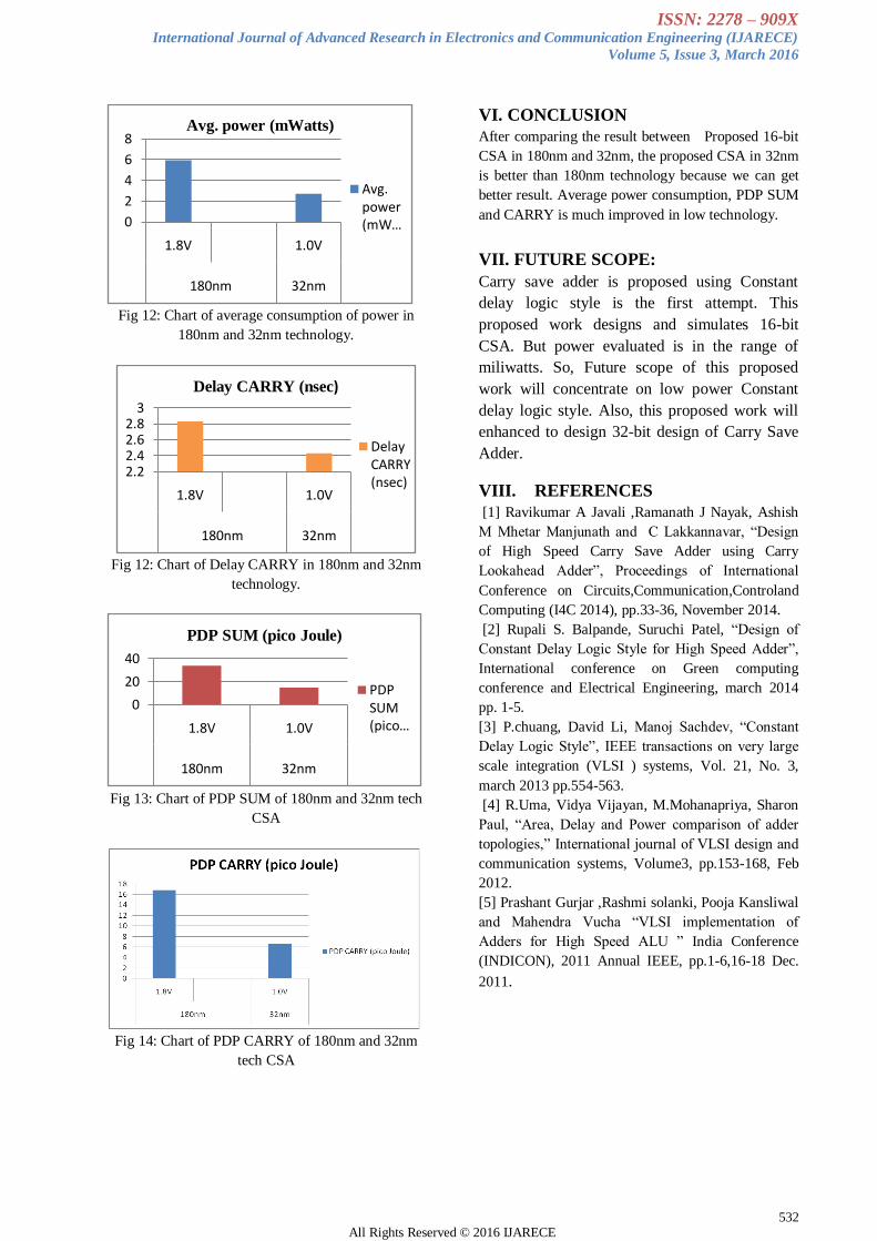
V. COMPARIOSN CHART
This chart shows the comparison of various
parameters in 180nm and 32nm technology and
from from this chart the researchers are able to
examine which technology is better.
Fig12: Comparison chart of Proposed CSA16-bit
CSA of 180nm and 32nm
ISSN: 2278 – 909X International Journal of Advanced Research in Electronics and Communication Engineering (IJARECE)
Volume 5, Issue 3, March 2016
532 All Rights Reserved © 2016 IJARECE
Fig 12: Chart of average consumption of power in
180nm and 32nm technology.
Fig 12: Chart of Delay CARRY in 180nm and 32nm
technology.
Fig 13: Chart of PDP SUM of 180nm and 32nm tech
CSA
Fig 14: Chart of PDP CARRY of 180nm and 32nm
tech CSA
VI. CONCLUSION
After comparing the result between Proposed 16-bit
CSA in 180nm and 32nm, the proposed CSA in 32nm
is better than 180nm technology because we can get
better result. Average power consumption, PDP SUM
and CARRY is much improved in low technology.
VII. FUTURE SCOPE:
Carry save adder is proposed using Constant
delay logic style is the first attempt. This
proposed work designs and simulates 16-bit
CSA. But power evaluated is in the range of
miliwatts. So, Future scope of this proposed
work will concentrate on low power Constant
delay logic style. Also, this proposed work will
enhanced to design 32-bit design of Carry Save
Adder.
VIII. REFERENCES
[1] Ravikumar A Javali ,Ramanath J Nayak, Ashish
M Mhetar Manjunath and C Lakkannavar, “Design
of High Speed Carry Save Adder using Carry
Lookahead Adder”, Proceedings of International
Conference on Circuits,Communication,Controland
Computing (I4C 2014), pp.33-36, November 2014.
[2] Rupali S. Balpande, Suruchi Patel, “Design of
Constant Delay Logic Style for High Speed Adder”,
International conference on Green computing
conference and Electrical Engineering, march 2014
pp. 1-5.
[3] P.chuang, David Li, Manoj Sachdev, “Constant
Delay Logic Style”, IEEE transactions on very large
scale integration (VLSI ) systems, Vol. 21, No. 3,
march 2013 pp.554-563.
[4] R.Uma, Vidya Vijayan, M.Mohanapriya, Sharon
Paul, “Area, Delay and Power comparison of adder
topologies,” International journal of VLSI design and
communication systems, Volume3, pp.153-168, Feb
2012.
[5] Prashant Gurjar ,Rashmi solanki, Pooja Kansliwal
and Mahendra Vucha “VLSI implementation of
Adders for High Speed ALU ” India Conference
(INDICON), 2011 Annual IEEE, pp.1-6,16-18 Dec.
2011.
0
2
4
6
8
1.8V 1.0V
180nm 32nm
Avg. power (mWatts)
Avg. power (mW…
2.22.42.62.8
3
1.8V 1.0V
180nm 32nm
Delay CARRY (nsec)
Delay CARRY (nsec)
0
20
40
1.8V 1.0V
180nm 32nm
PDP SUM (pico Joule)
PDP SUM (pico …


![Efficient Carry Select Adder Using VLSI Techniques …ijmetmr.com/olfebruary2015/AmarataMRohira-NAshokKumar-17.pdf2015/02/01 · gation in final stage of carry save adder [2]. Ramkumar](https://static.fdocuments.net/doc/165x107/5eb6574f49193e4e5c087655/efficient-carry-select-adder-using-vlsi-techniques-20150201-gation-in-final.jpg)