Design methodologies and techniques for production … · Design methodologies and techniques for...
127
1 Design methodologies and techniques for production low power SOC designs Dr. Kaijian Shi Synopsys Professional Services
Transcript of Design methodologies and techniques for production … · Design methodologies and techniques for...

1
Design methodologies and
techniques for production low
power SOC designs
Dr. Kaijian Shi
Synopsys Professional Services

2
Content
• Dynamic Voltage Frequency Scaling
• Power-gating design
• Production low-power SOC implementation
• Power intent definitions through UPF
• Production low-power design environment
• Summary
3
Dynamic Voltage Frequency Scaling (DVFS)
• Principles
• Workload based DVFS
• Adaptive VFS (AVFS)
• Application and PVT based VFS
• Production design considerations and
recommendations

4
DVFS Principles
CMOS Power, Energy and performance
P = Pdy + Pleak ~ C * v dd2 * f + vdd * Ileak
E = ∫ P * dt
f ~ (vdd-vt) / vdd 1.3
• Scale Vdd and f dynamically to just meet
performance needs
• Reduce f helps lowering power and thermal
but not energy (battery life) for a task
• Must reduce Vdd to save energy

5
Workload-based DVFS
• Workload – number of clock cycles to complete a task
• Deadline – latest time to complete the task
• DVFS – Reduce V and F to run just fast enough to meet the task deadlines and maintain quality of operations
100%
0%
100%
0%
DVFS
Energy Saved
Run/Idle
22
Reduce voltage
to lower level 1
1 Run task as
slow as possible
3
3Run task in
time available
4
4 Reduce voltage
to match time
3 4 5
3 4 5
21
Task-2

6
DVFS System
– OS-plug-in -> Pre-defined performance profiles (policies) -> predict workload and deadline of next task -> F -> look up V from F-V table
– Profiles are statistically generated and app-specific, e.g IEM for ARM cpu,
– F-V table is SoC block and process dependent
– DVFS controller is app-specific hardware
– Level shifters are needed at block interface
DVFS software
Look-ahead task
Predict workload
F =
V from F-V table
Programmable
V-regulator DVFS SoC block
Programmable
Clock generator
DVFS controller
Level shifters
deadline
workload
Other SoC blocks

7
• H-L: a simple buffer -
timing model differs from
normal buffers; characterized
with high input swing and low
output transition
Level Shifters
In (VddH) Out(VddL)
VddL
VddH
VddL
Out(0-VddH)
In(0-VddL)
• L-H: diff-amp buffer
• low-swing inputs (VddL)
• pull-up to VddH by diff-amp

8
IEM Testchip – SoC Implementation

9
DVFS Power and Energy saving
20% 40% 60% 80% 100%0%
100%
56%
23%
9%
300MHz, 1.21V
225MHz, 1.03V
150MHz, 0.81V
75MHz, 0.69V
20% 40% 60% 80% 100%0%
100%
75%
46%
36%
Power Energy
• 4 levels of DVFS

10
DVFS design considerations
• V-F scaling sequence
– Up-scaling: scale V -> settles -> switch F
– Down-scaling: scale F -> locked -> scale V
• Manage large clock skew due to V scaling
– fully asynchronous - synchronizer or FIFO
– Clock pre-compensation – shift launch clock earlier (max-skew) and add buffers to fix hold in short paths
• Above all, reliable app-specific DVFS software is essential – a real challenge!
– Sufficient app-runs to generate quality performance profile
– Conservative workload prediction

11
Clock latency variation with V-T (130um)
• Variation accelerates below 0.9V
Clock Tree Latency Analysis
2.362.227
1.962
1.568
1.207
1.064
0.96
3.626
2.963
2.187
1.741
1.333
1.079
1.66
0.733
1.483
0.5
0.6
0.7
0.8
0.9
1
1.1
1.2
1.3
1.4
1.5
0.0
0.5
1.0
1.5
2.0
2.5
3.0
3.5
4.0
Latency (ns)
Vo
lta
ge
(V
)
Latency[FF]
Latency[TT]
Latency[SS]
Delta = 1ns (50%)
• Much worse in
weak corner -
50% (1V-0.8V)

12
Adaptive voltage frequency scaling (AVS)
Programmable
V-regulator
DVFS SoC block
Programmable
Clock generator
AVS controller
Level shifters
• Based on on-chip performance monitor
• Close-loop system for process and temperature compensation
monitorLevel shifte
rs

13
AVS design considerations
• On-chip performance monitors
– Ring oscillator sensing PVT variation
– Power & area overhead mitigation
– Multiple monitors placed in chip centre and four corners
• AVS controller
– Reliable algorithms for loop stability in discrete V-F scaling
– Short enough loop response time to prevent VF oscillation
• Mixed analog-digital physical implementation
– Analog/digital isolations (guide rings etc.)
– A/D block interface signalling
– A/D power grids separations

14
Application based VFS
• Pseudo-dynamic V-F scaling based on application needs (e.g. voice vs. video)
• Switching before an app-execution
• Simpler design -> lower risk impact on yield, TTM
– A few V-F levels and hence manageable PVT variations
– Full corner timing closure is feasible for high yield
– No sensors and complex scaling control
– Not depend on workload profiling
• Less efficient than DVFS and AVS
• Not for PVT compensation

15
An example: Intel Turbo Boost
• Clock scaling constrained by T and IR-
drop to boost performance
• For a high-performance application,
increase clock frequency by 133MHz a
step, until reaching defined T or IR-drop
limit
• Only scale clock and hence not for energy
saving

16
IBM EngerScale for Power core
• Static Power Saver Mode
– User control (on/off) for predictable workload change
– Lower V-F with safe margin
• Dynamic Power Saver Mode
– DFS based on core utilization and policies configured by user
– Favor Power: default at low F, increase under heavy utilization
– Favor Performance: default at max F, decrease when lightly utilized or idle

17
Production design considerations and
recommendation – V-F scaling
• V-F scaling
– Min V = 1.8~2 * Vt
• Too big variation to manage when noise margin < Vt
• T-inversion at low Vdd make the case even worse
– Max 4 scaling levels (design corners and closure concerns)
– Up to 2 Vt cells in a VFS domain to maximize VF scaling range and PVT variation tolerance
• V-regulator
– Avoid on-chip regulator (linear regulator does not reduce chip P & E; bulk regulator is too noisy)
– Programmable off-chip regulator is often the choice
– Watch regulator’s settling time (10’s-100’s us) – custom design regulator to reduce settling time as needed

18
Production design considerations and
recommendations - VFS
• Clock generator
– Can be embedded in the SoC and combined with SoC clk-generator for efficiency
– Watch clock locking time – good PLL to meet req
• Block interface timing challenge due to large clock skew in large V variation in scaling
– Async interface (sync-cell or FIFO), if applicable
– Clock pre-compensation – shift launch clock earlier by max-skew-variation and add buffers to fix hold violations in short paths

19
DVFS vs. AVS vs. App VFS vs. PVT DVFS
• Things to consider:
– Actual P&E saving considering added P/E overhead (P&E on DVFS logic and scaling operations)
– Area penalty
– Design closure and verification – QoR and TTM
– IO standards do not scale!
– Reliability and cost
• A good choice for production design:
Chip-level, app-based VFS combined with PVT DVFS, fixed V on standard IOs

20
Content
• Dynamic Voltage Frequency Scaling
• Power-gating design
• Production low-power SOC implementation
• Power intent definitions through UPF
• Production low-power design environment
• Summary

21
Power-gating design
• Principle
• System and components
• Retention strategies and techniques
• Production design considerations and
recommendations

22
Power gating principle
• Leakage trend
L-VTH logic cells
Vss
Vdd
sleep
Virtual Vss
Virtual Vdd
sleep
0
50
100
150
200
250
250 nm 180 nm 130 nm 90 nm 65 nm
Leakage Power
Dynamic Power
Po
wer
(Watt
s)
0
50
10
0
15
0
20
0
25
0
25
0
180 13
0
90 65
Technology (nm)

23
Power gating system components
• Shut-down and ao domains
• PM unit
• ao-buffers
• Switch cells
• Isolation cells
• Retention rams
• Retention flops
ISO
Shut-down
domain 2
Retention
Memory
Shut-down
domain 1
PM
Always-
on
domain
ISO
RR
ao

24
Power Management (PM) Unit
CLOCK
N_ISOLATE
N_RESET
SAVE
RESTORE
N_PWRON
• Control sleep/wakeup sequence
– Clocks – architecturally suppress during sleep
– Isolation – control clamping of outputs pre-sleep
– Retention – control save and restore states
– Resets – put the block in “quiet” state pre-/after-sleep
– Power-Down – when to shut-down and wakeup a block

25
Always-on repeaters
• Distribute signals through shut-down domains
• Dual rail buffer/inverter with AO-power pinVDD rail is not used; VDDC connects to AO-power
No placement restriction
VDD
VDDC
VSS
• Normal buf/inv – placed them in dedicate regions with separated ao-rail

26
Switch cells
• Custom-designed HVtpMOS for header switch and nMOS for footer switch
• Optimized (L,W,BBS) for max efficiency (Ion/Ioff)
4.00E-07
2.40E-06
4.40E-06
0
5000
10000
15000
20000
25000
6.5
0E
-8
9.5
0E
-8
1.2
5E
-7
1.5
5E
-7
Wgate
Ion/Ioff
Lgate
TSMC 65g pMOS : Ion/Ioff (Vdd=1, Vbb=1v)
• Integrated repeaters
• Single/dual switch cell
VDD
Pon
Pon-ack
VDDC Pon1 VDDC Pon2
VDDPon-ack1 Pon-ack2

27
Signal isolations
• isolation methods
– Retain “1” isolation circuit
– Retain “0” isolation circuit
– Retain current state circuit
Retention flop
• Output isolations
– Pros – simple control
– Cons – ao-cell and ao-power
• Input isolations
– Pros - Normal std_cells and Less power (floating input)
– Cons - Complex control on inputs that connect to power-down outputs
VDD
Gnd
ISO
IN
ISO_out
IN
ISO_out
ISO
VDDC
Gnd
ISO
IN
ISO_out
ISO_outISO
IN

28
Power-gating design
• Principle
• System and components
• Retention strategies and techniques
• Production design considerations

29
State retention in shut-down period
• Needed to fast resume operations after wakeup based on the states at shut-down
• Retention through live memories
• Retention registers
• Retention rams
• Production design considerations and
recommendations

30
Retention through live memory
1. Write/read states to/from live memory, before sleep and after wakeup
– Proc: simple (software)
– Cons: long retention/restore latency
2. Scan in/out states to/from the memory
– Proc: shorter latency
– Cons: retention-based flop stitching may conflict optimal DFT scan stitching
• Much longer latency than retention registers

31
Balloon style retention register
• Add an always-on high-Vt balloon latch for state retention.
• Pros:
Low leakage and performance impact due to minimum size and low coupling of the balloon latch
• Cons:
1. Require two global control signals to save and restore state
2. Large area penalty (30%)

32
Control sequence
– save/restore retention register
CLOCK
N_ISOLATE
N_RESET
SAVE
RESTORE
N_PWRON

33
“Live Slave” DFF (posedge)
• HVt ao-slave latch
• Clamp clock to separate slave latch from the register in power-down.
• Pros: Single ret-control signal
• Cons:
1. Performance hit due to HVt latch and NAND in clock to Q path
2. Power penalty due to NAND in clock
CK
CKN
CKN CK
SI
SE
D
CK
CKN CK
CKN
SE SEN
SEN
SEN
QCK
CKN
CLK
RETAIN
Power-Gated Supply
Hi-Vth, Always-On
supply
Master Latch Slave Latch
T1

34
Control sequence
- Alive Slave style retention register
CLK
PG_ENABLE
NRETAIN

35
Pulsed Latch Base Design
FF 124668
Pulse latch
replacement
124067
No
replacement
601
Pulse
generator
9
Pulsed Latch
•Pulse generator
insertion
•Dummy block insertion
•Pulse latch replacement
•Power and timing
analysis
PL:Pulsed Latch
PG:Pulse Generator
PL
Mem
PL
PL
FF
PG
Dummy
PL:Pulsed Latch
PG:Pulse Generator
PL
Mem
PL
PL
FF
PG
Dummy
FF
Mem
FF
FF
FF
FF
Mem
FF
FF
FF
• Results (2M Gates) • Dynamic power reduction: 25%
Power (mW)
Sequential Combinational Total
Dynamic Leakage Total Dynamic Leakage Total Dynamic Leakage Total
F/F 121.98 0.683 122.7 76.02 0.196 76.22 197.96 0.880 198.9
Pulse
Latch
67.12 0.344 67.46 81.63 0.704 82.33 148.74 1.048 149.8
Ratio -45.0% -49.6% -45.0% 7.4% 259.2% 8.0% -24.9% 19.1% -24.7%
Courtesy of Nobuyuki Nishiguchi (STARC)

36
Low Power Testable Static Pulse-triggered Flip Flop
with Reset and Retention - LPTSPFFRR
• Diff-input-latch for min latch size and low clock power
• Concise design: 3 NMOS and live latch for retention: 2 NMOS for reset
• R2 to prevent contention with input and P3 to prevent state corruption
• Delayed SQ latch; HVt transistors are used in test part to reduce leakage
D
SE
SEN
SI
Q
PL
SQ
PL
PLN
xT2
SE
PL
SE SEN
PLN
SEN
RETN
CLR
RETN
PLN
Always-On
P1
P2
P3
R1
R2
Kaijian Shi – ICCD08

37
Save and restore sequence
Reset :
– Async reset in normal operation mode
– No effect in retention mode (preserve flop state)
PL
RETN
PWR
CLR
38
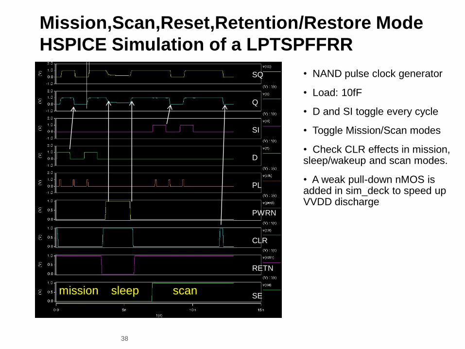
Mission,Scan,Reset,Retention/Restore Mode
HSPICE Simulation of a LPTSPFFRR
• NAND pulse clock generator
• Load: 10fF
• D and SI toggle every cycle
• Toggle Mission/Scan modes
• Check CLR effects in mission, sleep/wakeup and scan modes.
• A weak pull-down nMOS is added in sim_deck to speed up VVDD discharge
SQ
PWRN
CLR
RETN
SE
Q
SI
D
PL
mission sleep scan

39
Retention technique comparison
• Retention latency constrains the choice of the retention techniques
• Power overhead on saving and restoring states depends on number of states
• No chip power overhead with external non-volatile ram retention
• Overall power saving depends on sleep period
• Mode-dependent retention considerations (light/deep sleep, hibernate, shut-down)
impact Area Latency P-save/restore P-retention
Ram
read/write
None Long High Low/None
(size/external)
Ram
scan/DMA
Low Medium Medium Low
Retention
flops
High Low Low Low
40
Retention memory
• RAM power is mainly leakage which becomes significant due to increasing RAM size
• Ram leakage reduction in retention mode
– Diode source biasing – fixed biasing
– Dual source biasing – tunable biasing
• Ram leakage reduction in function mode
– Drowsy ram – diode source biasing
– Drowsy ram – tunable source biasing
• Considerations and recommendations

41
Diode source biasing
V_VSS
VSS
SLEEPN
VDDVDD
• Fixed bias (Vgs)
• Diode power overhead
• Raise Vss to :-
• Reduce array cell voltage
• Reverse bias NMOS

42
Tunable source biasing
VVSS
SLEEP
VDDVDD
VSS VSLEEP
SLEEP
• Tunable bias (Vsleep)
• Low power overhead – no diode power
43
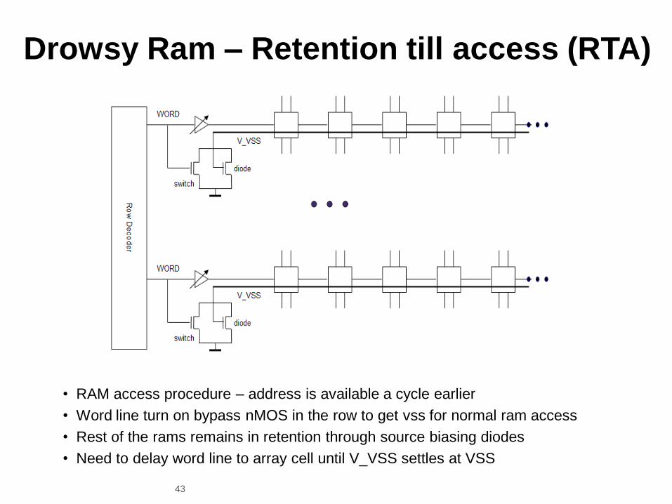
Drowsy Ram – Retention till access (RTA)
• RAM access procedure – address is available a cycle earlier
• Word line turn on bypass nMOS in the row to get vss for normal ram access
• Rest of the rams remains in retention through source biasing diodes
• Need to delay word line to array cell until V_VSS settles at VSS

44
Drowsy Ram (RTA) – tunable source bias
45
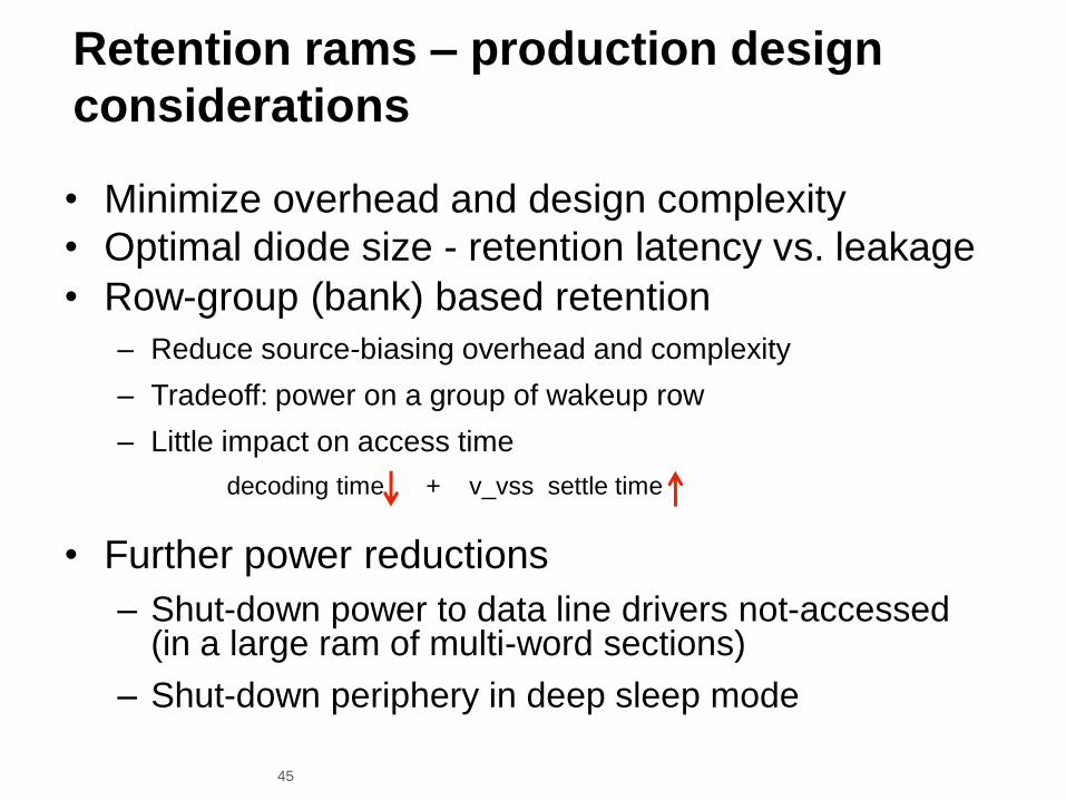
Retention rams – production design
considerations
• Row-group (bank) based retention
– Reduce source-biasing overhead and complexity
– Tradeoff: power on a group of wakeup row
– Little impact on access time
decoding time + v_vss settle time
• Minimize overhead and design complexity
• Optimal diode size - retention latency vs. leakage
• Further power reductions
– Shut-down power to data line drivers not-accessed (in a large ram of multi-word sections)
– Shut-down periphery in deep sleep mode

46
Power-gating design
• Principle
• System and components
• Retention strategies and techniques
• Production design considerations

47
Power-gating benefit – theory vs. real
• Idle power saving = Pnormal / Pgated
• Switch is far from ideal
Leaky in shut-down and sw-vdd is not close to 0
• Idle power saving measured from a testchip
– TSMC90G chip: 15-24x (-10C to100C)
– TSMC65LP chip: 6-26x (-10C to100C)
• How about off-chip power gating?– Close to ideal switching => max saving! BUT :
– Significantly long wakeup latency
– Noise to live logic through GND due to rush current
– High cost and complexity in chip applications

48
90G - RELATIVE LEAKAGE POWER SAVINGS - STD CELL
(OVER PORTABLE BATTERY PRODUCT TEMP RANGE)
0.0
5.0
10.0
15.0
20.0
25.0
30.0
Temperature
HA
LT
:SR
PG
Rati
o
HALT:SRPG
HALT:SRPG 14.3 17.9 21.3 23.0 24.2 24.2 23.1 22.9 21.8 20.7 19.1 17.7
-10 0 10 20 30 40 50 60 70 80 90 100
Power Gating Efficiency – TSMC90G
• Pnormal / Pgated varies with T
~ 24x saving at 35°C

49
65LP - RELATIVE LEAKAGE POWER SAVINGS - STD CELL
(OVER PORTABLE BATTERY PRODUCT TEMP RANGE)
0.0
5.0
10.0
15.0
20.0
25.0
30.0
Temperature
HA
LT
:SR
PG
Rati
o
HALT:SRPG
HALT:SRPG 6.9 8.4 11.7 14.6 18.8 22.4 24.9 26.1 25.9 24.8 22.9 20.6
-10 0 10 20 30 40 50 60 70 80 90 100
Power Gating Efficiency – TSMC65LP
• Pnormal / Pgated is more T sensitive in 65LP
~ 26x saving at 65°C

50
Power-gating overhead
• Area overhead
– New cells (controller, sw, iso, ls, ao-buffer tree)
– Retention cells size (save/restore registers are
30% larger)
• Power overhead
– New cells: pm logic and buffer trees
– PM operations: State retentions, wakeup
charging power, state restorations

51
Power-gating negative impacts
• Impact on performance
– Wakeup latency (charge-up and restore states)
– Slow PM cells (retention flops, iso- and ls-cells)
– Switch IR-drop caused cell delay degradation
• For case study 5% IR drop -> 9% delay degradation and for 10% voltage drop -> 27% lower performance
• Impact on power integrity – if not managed
– Wakeup rush current could cause large IR-drop in live logic and malfunction
– Complex switched power grid is error prone
• Impact on schedule
– Complex design takes longer to implement and even longer to verify (pm sequence, pm modes combinations …)
52
Content
• Dynamic Voltage Frequency Scaling
• Power-gating design
• Production low-power SOC implementation
• Power intent definitions through UPF
• Production low-power design environment
• Summary

53
Production low-power SOC implementation
Correct strategies and attention-to-details are keys to success
• Process selection
• Power domain partitioning considerations
• Central vs. Hierarchical PM control
• Retention strategies
• Switch power network design
• Things to watch in the implementation

54 54
Process selection based on power gating
efficiency
• Leakage saving is more efficient in LVt, specially at high temperature
• Limited leakage saving (5x) in LP and HVt combination
• Yet, HVt leakage is 1.5-2x lower than N/LVt ; LP process leakage is 65-200x
lower than G process => Choose LP/ HVt when standby leakage is primary
concern and design it not timing critical

55 55
Process selection considering power-delay
efficiency (P*D product)
• Power needed for normal operation; lower P*D -> higher efficiency
• Differences in Vt and T are not significant
• G-process is more efficient than LP
• Choose G-process if operational power reduction is critical or design is
timing critical (area and power explosion)

56
Normal Idle EIdle E saving
Actual Power/Energy saving -
operation profile dependent
Mission
E
Mission
E
Power
TimeShut-down E
Save state E
Charge+restore E

57
Power domain partition considerations
• Key: power saving must overwhelm overheads
• Consider domain operation profile
– Idle rate = tidle/tactive (should be high enough)
– idle period should be much longer than wakeup’s
• Size – small domain does not worth the effort
• Timing criticality
– Can chip performance tolerate wakeup latency?
– Can inter-block paths meet timing with isolation cells?
– Enough timing margin for delay degradation?
• Functional/logic hierarchy and interface complexity

58
Central vs. hierarchical PM control
• Central PM – global PM control
– Less complex to implement and verify
– Global PM control distribution
• Hier-PM – each block has a local PM
– Suitable when a block needs complex control to take care of pending jobs and handshakes before going into sleep
• Choose central PM if design does not requires complex chip/block pm control
• Good practice: reset before sleeping to minimize shut-down noise to live logic
• Consider test needs – all live vs. gated test; controllability at tester

59
Retention strategy recommendations
• Sleep mode retentions (Choice in preference order)
– Avoid retention if you can (if app does not impose that)
– Consider retention through live memory strategy, if retention latency does not cause wakeup latency constraint violations
• Save and restore states in retention rams if already in a design
• Save and restore states in an always-on memory, otherwise
– Consider single-control “live slave” retention flops, if flop o/p paths are not timing critical
– Explore partial state retention if full retention is deemed too expensive in area overhead. Watch out for DV complexity.
• Ensure proper reset non-retained states at wakeup to prevent X propagation – DV complexity
• No dead lock at wakeup

60
Retention strategy recommendations
• Mission mode power reduction with RTA rams
– On selected rams, based on operation profile and timing: • low access rate – e.g. L2/L3 cache
• not in a timing critical path – due to longer access time
• Retention rams implementations– Consider diode source biasing rams for easy implementations
– Consider tunable source biasing rams for large rams where the extra power supply to the rams bias can be justified by the considerable idle power saving
– Take care of mode switching sequence and timing constraints
• Ret-rams may not work in illegal PM transition states
• Must meet PM state switching timing constraints in IP spec, including signal hold time and wait period
– Check if ram’s inputs are isolated during retention. If not, need to clamp ram inputs
– Low noise on ram array supply to prevent data corruption

61
Switch P/G network design
Mission-mode pg grid design to meet IR-
drop and EM constraints
• Network style
• Switch cell – type and number
• Switch pg network synthesis
Switch P/G network
Design
Power-up Sequence
Design
Static IR-drop and EM
Analysis
Dynamic wakeup rush
current and IR-drop
Analysis
Wakeup latency and in-rush current control
• Switch turn-on sequence control
Determine product’s power-gating
efficiency and QoR
Impact performance, power integrity
and schedule

62 62
Switch power network style selection –
Ring style
• Good choice for a domain not needing always-on power in the domain
• Easy power planning: separate vdd and vvdd, switches outside domain,
conventional internal pg grid generation
• Need sufficient via arrays for switches/rings connections (IR-drop/EM)
• Do not pack ring switches and check impact on IO routability

63 63
Switch power network style selection –
Grid style
• Smaller area penalty and better power integrity than ring-style
• Good choice for a design that requires always-on power in domain
• Suggest to implement power-gating RAMs and IPs to avoid otherwise
challenge local switch rings for those RAMs and IPs.
• Thick top metal for VDD and lower metal for VVDD

64
Recommendations - Ring vs. Grid style
• Choose Grid style for a design if:
– It implements retention registers
– It does not have many macros
– It requires pushing leakage down to limit
• Choose Ring style for a design if:
– No need permanent VDD in the power-gating blocks
– Power-gating blocks are not too large to build virtual
P/G network that meets IR-drop target
– No too many block IOs to route through switch rings
• Hybrid (Grid + macro-ring) only when needed
65 65
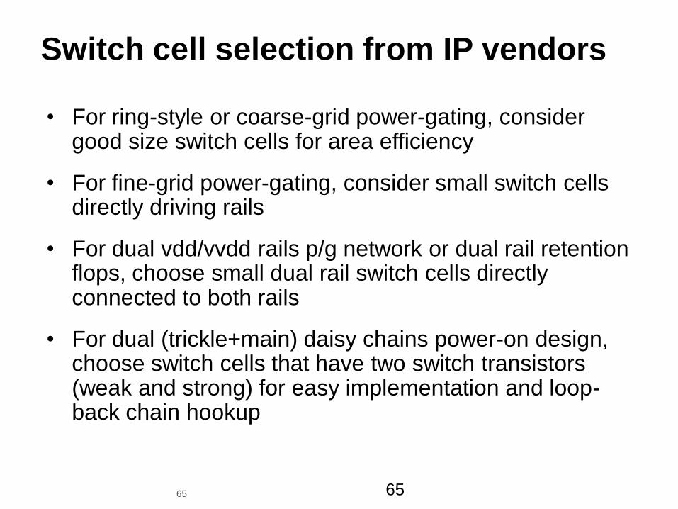
Switch cell selection from IP vendors
• For ring-style or coarse-grid power-gating, consider good size switch cells for area efficiency
• For fine-grid power-gating, consider small switch cells directly driving rails
• For dual vdd/vvdd rails p/g network or dual rail retention flops, choose small dual rail switch cells directly connected to both rails
• For dual (trickle+main) daisy chains power-on design, choose switch cells that have two switch transistors (weak and strong) for easy implementation and loop-back chain hookup

66
Number of switch cell
• Power based estimation method
N_switch = K * (P / Vdd) / Ids
Where
• K is the safe margin factor (1.5 – 2.0) covering NBTI, variation, etc.
• P is the worst-case average power
• Vdd is supply voltage
• Ids is switch current when Vds = switch IR-drop target

67
Switch P/G network synthesis
• Quality of switch P/G network is determined by both
switch cell and P/G mesh designs which requires:-
• Simultaneously optimize VDD, switch cells, VVDD
• Optimal switch insertion and P/G mesh strap pitches
and widths for min area and max routeabillity meeting
a given IR-drop target
• Fake via concept to model switch cell drive, layout
positions and physical connections. This enables
leveraging existing industrial power network synthesis
methods and tools

68
Switch power network modeling
VDD
network
Sleep
transistor
Cell current
sinks
VVDDnetwork
Cell current sink: worst-case average cell current
-- from power estimation or power analysis
Sleep
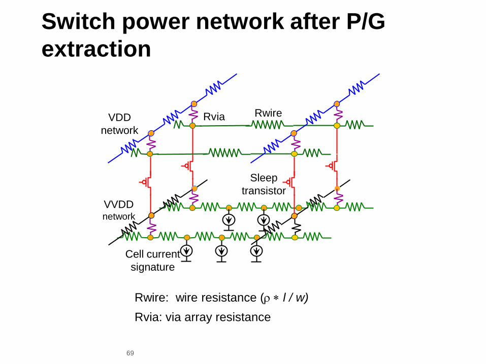
69
RwireRviaVDD
network
Sleep
transistor
Cell current
signature
VVDDnetwork
Switch power network after P/G
extraction
Rwire: wire resistance (r * l / w)
Rvia: via array resistance

70
Resistive power network
with fake vias
RwireRviaVDD
network
Fake via
Cell current
signature
VVDDnetwork
Gv = i (NA)
G = conductance matrix
v = nodal voltages
i = current sources
Rfake_via: r = DVds/DId, x,y = sleep-t position
Vdd
Ax = b (MNA) -- Eq.1
• A and b can be
obtained by MNA
generation rules
• Linear equation
can be solved by
efficient matrix
solver

71
Switch power network synthesis
– Optimization problem
min (w*Asleep + Astraps)
IRn < IRtarget
| jm | < jEM
where
Asleep is total silicon area of the sleep transistors
Astraps is total metal area of VDD and VVDD net wires
w is weight
IRn is IR drop on node n and IRtarget is defined IR drop target
jm is current density of VDD network branch m
jEM is maximum current density defined to prevent EM violations

72
Synthesis flow
Generate initial sleep transistor P/G network
Form Eq. 1 from current sleep transistor P/G network
Solve Eq. 1 and calculate IRn and jm
Evaluate Objective function
Converge?
Generate next step opt variables (solver)
Adjust variables with constraints
Replace fake vias by sleep transistor
finalize the sleep transistor P/G network
Yes

73
Wakeup latency and rush current
• Wakeup latency – mainly the time to charge a design to a full power-on state
– Performance hit and application constraints
• Large charging current at wake up
– Simultaneous charging power nets
– Crowbar current
– Large IR-drop malfunction, data corruptions
• Optimal wakeup control
– Minimize peak rush current while meeting max charge-up latency requirement
• A practical solution
– Daisy chain style power-on sequence

74 74
Wakeup rush current control –
Single daisy chain
• Sequentially turn on switches to limit charge current
• Fully turn-on time is determined by buffer delay and chain length
• Rush current is constrained by switch size and buffer delay

75 75
Wakeup rush current control –
Dual daisy chains
• Small transistors to form weak chain that trickle charge design at wakeup
• Strong transistors to form main chain that fully charges design
• Low rush current (small T at wakeup and small delta-V when main T on)
• Check if chain delay cause issue in wakeup latency constraint

76
Loop-back weak+main chain
• Explore built-in twin switch and buffers to ease daisy chain routing
VVdd
Pwr-On Pwr-Ack

77 77
Wakeup rush current control –
Complex daisy chains
• Parallel short chains to reduce charge-up time
• Sequentially turn on the short chains to control rush current

78 78
Wakeup rush current control –
Programmable daisy chains
• For 1) Application specific charge-up time 2) T-based adjustment
• App (software) programmable daisy chains to meet app and T req.
• Different length chains controlled by PM registers based on program

79 79
Wakeup analysis – dynamic IR-drop analysis
• Switch cells are modelled by I-V curve from SPICE char
• Transient P/G network solver to calculate charge current and ramp-up voltage
Fast charge-up:
• Short weak chain and 5ns delay of main chain-on time
Slow charge-up:
• Short weak chain and 20ns delay of main chain-on time

80 80
Wakeup control – recommendations
(in order of preference)
Based on wakeup latency constraint, domain size, and switch size and
placement
1. Consider loop-back (trickle+main) daisy chain for easy
implementation and good rush current control, if the chain delay
meets wakeup latency
2. Use dual daisy chain structure if wakeup latency constraint is app-
dependent. Let application control chain hookup
3. For tight wakeup latency constraint, consider parallel short daisy
chains. Check dynamic IR-drop in live-pg-grids
4. Consider programmable wakeup control method, if design will
operate at large voltage and temperature variations, and wakeup
latency constraint varies significantly with applications.

81 81
SW Power network design - Summary
• Quality of switch P/G network design has strong impact on
effect of power-gating design
• Power integrity and sleep mode leakage of a power-gating
design is determined by switch P/G network design
• The wakeup latency and rush current are controlled by
proper switch turn-on sequence configurations
• The IR-drop effect of rush current on alive blocks can be
mitigated by distance rush current sources from alive blocks
• Static and dynamic IR-drop/EM analysis are needed for
switch P/G network design and power-up sequence
configuration respectively

82 82
Things to watch out for in power-gating
production design
• Clock tree integrity - domain aware CTS
• DFT testability - domain aware DFT insertion
• Global control integrity - always-on logic synthesis

83
Power island aware CTS
• Avoid clock tree broken by a power-down block
• Island based subtrees
• Top-level CTS
– Balance to subtrees
– Metal connections to subtree root buffers
– Use always-powered buffers for long nets cross power islands
Island 2
Always-on
IslandIsland 1
Island 3
Island CTS
tree

84
Domain-aware DFT• All live chip test - test power could be too large, simple DFT
– Scan chains can cross domains, though may need LS at interface
– Watch out for deadlock in Pwr-on-reset (e.g. ram efuse chain)
PD1PD2
PD top
0.9V 0.7V1.1V
voltage_mixing false
pd_mixing false
PD1PD2
PD top
0.9V 0.7V1.1V
voltage_mixing true
pd_mixing true
• Allow shut-down blocks in chip test – low test power, complex DFT– Domain-based scan chains
– Maintain tester controllability

85
Always-On (AO) logic synthesis
• Ensure signal controllability in sleep mode
• AO net identification
– Designer define
– Trace from AO block ports and macro pins
• Logic/nets in fanin cone to an AO port/pin are AO
– Based on related supply nets of ports/pins
• Assumption: single switched supply, any other supplies are AO supplies and require AO drivers
• Domain-based AO logic insertion
– AO cells in shut-down domains and normal cells in AO domains
– Watch out for:
• AO cells in AO domains waste area and complexity
• AO in shut-down nets cause short-circuit power (floating input)

86
Domain-aware AO synthesis
• AO-buf in shut-down domains
• normal-buf in always-on domains
AO-buffer
normal buf
PD_1 TOP – always-onPD_3
PD_2
AO net
Feedthrough

87
Port/pin-aware AO synthesis
• AO-buffers drive domain AO
ports or macro AO pinsAO-buffer
normal buf
TOP – always-on
PD
Low-
power
ram
AO pin
AO port

88
Content
• Dynamic Voltage Frequency Scaling
• Power-gating design
• Production low-power SOC implementation
• Power intent definitions through UPF
• Production low-power design environment
• Summary

89
UPF – IEEE 1801 (Power Intent spec)
Functional intent defined in RTL
• Architecture
• Design hierarchy
• Data path
• Custom blocks
• Application
• State machines
• Combinatorial logic
• I/Os
• EX: CPU, DSP, Cache
• Usage of IP
• Industry-standard interfaces
• Memories, etc
Power intent defined in UPF
• Power distribution architecture
• Power domains
• Supply rails
• Shutdown control
• Power strategy
• Power state tables
• Operating voltages
• Usage of special cells
• Isolation cells, Level shifters
• Power switches
• Retention registers
• RTL extension; understood by DV and Implemenation tools

90
UPF - a simple conceptual design
• Power Intent
– 3 Power Domains
• Shut-down (0.864V)
• AO (1.08V)
• Top (0.864V)
– Retention FF required
– LS/ISO cells requiredctrl
flop_AON
top_sd
top
1.08V 0.864V
0.864V
save
restore
ISO
ISO
isolate_enable
RFF
RFF
LS
on/off
sleep
91
Create Power Domain in UPF
• create_power_domain
– 2+1 Power Domains
• 1.08V
• 0.864V
• Top Level
ctrl
flop_AON
top_sd
top
1.08V 0.864V
0.864V
save
restore
ISO
ISO
isolate_enable
RFF
RFF
LS
on/off
create_power_domain TOP_PD
create_power_domain FLOP_AON_PD
-elements {flop_AON}
create_power_domain FLOP_SD_PD
-elements {top_sd}
sleep

92
Create Supply Net/Port in UPF
• Create Supply Net
• Create Supply Port
• Connect Supply Net to Port
ctrl
flop_AON
top_sd
top
1.08V 0.864V
0.864V
save
restore
ISO
ISO
isolate_enable
RFF
RFF
LS
on/off
create_supply_net VDD_AON
-domain FLOP_AON_PD
create_supply_port VDD_AON
-domain FLOP_AON_PD
connect_supply_net VDD_AON
-ports VDD_AON
set_domain_supply_net FLOP_AON_PD
-primary_power_net VDD_AON
-primary_ground_net VSS
VDD_AON VDD VSS
sleep

93
Create Power Switch in UPF
• Create Shut-Down Logic
– Define Power Switch
– Map Power Switch
ctrl
flop_AON
top_sd
top
1.08V0.864V
0.864V
save
restore
ISO
ISO
isolate_enable
RFF
RFF
LS
shut_down
create_power_switch flop_header
-domain FLOP_SD_PD
-input_supply_port {sw_in VDD}
-output_supply_port {sw_out VDD_SD_V}
-on_state {all_on_state sw_in {shut_down}}
-control_port {sleep shut_down}
map_power_switch -domain FLOP_SD_PD
-lib_cell HDRDID2HVT flop_header
VDD_AON VDD
VDD_SD_V
VSS
sleep

94
Define Isolation Cell Strategy
• Define Isolation cell
Strategy
– Type of Isolation cell
– Clamp Value
– PG Hookup
– Location of Isolation cell
ctrl
flop_AON
top_sd
top
1.08V 0.864V
0.864V
save
restore
ISO
ISO
isolate_enable
RFF
RFF
LS
on/off
set_isolation ISO
-domain FLOP_SD_PD
-clamp_value 1 -applies_to outputs
-isolation_power_net VDD
-isolation_ground_net VSS
set_isolation_control ISO
-domain FLOP_SD_PD
-isolation_signal {ctrl/isolate_enable}
-location parent
VDD
VSS
1/0
1/0
ISO
VDD_AON
sleep

95
Define Level Shifter Strategy
• Define LS strategy
– Rule
– Location
ctrl
flop_AON
top_sd
top
1.08V 0.864V
0.864V
save
restore
ISO
ISO
isolate_enable
RFF
RFF
LS
on/off
set_level_shifter ls_in_flop_aon
-domain FLOP_AON_PD
-applies_to inputs -rule both
-location self
set_level_shifter ls_out_flop_aon
-domain FLOP_AON_PD
-applies_to outputs -rule both
-location parent
VDD
VSS
LS
VDD_AON
sleep

96
Define Retention Strategy
• Define Retention Strategy
– PG Hookup
– Control Signal
– Lib Cell
ctrl
flop_AON
top_sd
top
1.08V 0.864V
0.864V
save
restore
ISO
ISO
isolate_enable
RFF
RFF
LS
on/off
set_retention RFF -domain FLOP_SD_PD
-retention_power_net VDD
-retention_ground_net VSS
-elements {top_sd/flop_RET}
set_retention_control RFF
-domain FLOP_SD_PD
-save_signal {ctrl/save low}
-restore_signal {ctrl/restore high}
map_retention_cell RFF
-lib_cell_type RSDFCD1
-domain FLOP_SD_PD
VDD
VSS
LS
VDD_AON
sleep

97
Defining Valid States
Allowed transitions
Disallowed transitions
BOOT
ALL_ON
OFF VDD VDD_AON VDD_SD VDD_SD_V
OFF TOP_ON FLOP_AON SD_OFF SD_OFF
BOOT TOP_ON FLOP_AON SD_AON SD_OFF
ALL_ON TOP_ON FLOP_AON SD_AON SD_AON
98
Content
• Dynamic Voltage Frequency Scaling
• Power-gating design
• Production low-power SOC implementation
• Power intent definitions through UPF
• Production low-power design environment
• Summary

99
Design environment for production low
power design
• Manage complex low-power design flow
• Implement fine-tuned strategies and
techniques for production designs
• Minimize human mistakes and flow errors
• Smooth design data transactions between
tools and flow steps
• Ease-to-Use, QoR, fast TTM
10
0
Lynx Design System OverviewFour Components of Lynx
Open environment for flow
development and execution
• Production Flow– Open, proven production flow in use to
28nm
– Integrated low power methodologies
– Integrated ARM-Synopsys
implementation RM’s
• Runtime Manager– Graphical flow creation, configuration,
execution, and monitoring
– Rapid design exploration
• Management Cockpit– Unique visibility into design status, trends
– Works in conjunction with the Runtime
Manager to provide a complete
environment
• Foundry-Ready System– Pre-validated IP, libraries, tech files and
library preparation collateral
– Automated and manual tape out checks
10
1
Lynx Production Flow
Production Flow Tasks
Flow Steps
Global Analysis Tasks
STA SI Power MVRC ATPG EM/IR
Chip
Finishing
Synthesis
& DFT
Design
Planning
PNR
Optimization
•Fill Cell, Fill Metal
•Final Extraction
•Timing Closure
•DRC/LVS
•View Generation
•Virtual Flat
•1801 UPF Support
•Power Mesh
•Proto Route & IPO
•Pin Assignment
•Budgeting
•Placement
•HFNS & CTS
•Route Opto
•MCMM & 1801
•Power Closure
•SI Closure
•Synthesis
•Clock Gating
•Gate Optimization
•DFT Scan
•Compression
•JTAG
• Proven from 180 to 28nm; over
100 tapeouts
• Incorporates Synopsys RM’s for
optimal tool results
• Advanced methodologies built in
(e.g., Low Power, MCMM)
• Fully tested with multiple
foundries, libraries, &
technology nodes
• Synopsys supported and
regularly updated

10
2
Design Vision Visual UPF
Strategies VisualizationSupply port
Block PD primary
power net
Retention register
Top PD primary
ground net LS strategy
defined in UPF
ISO location
parentwith
backup power
defined
Power
Switch
PD boundary
10
3
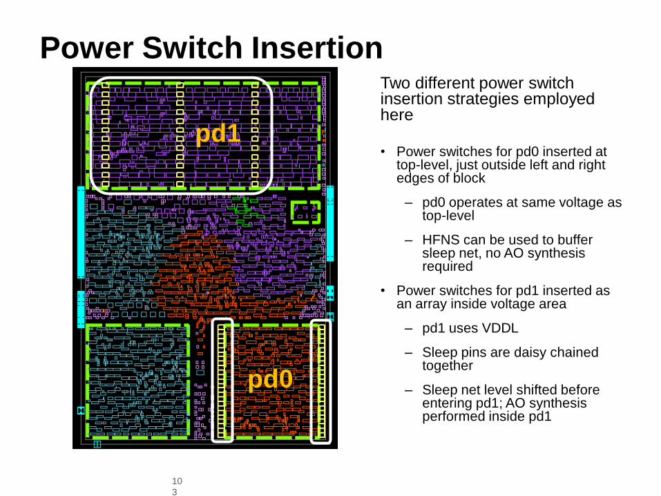
Power Switch InsertionTwo different power switch insertion strategies employed here
• Power switches for pd0 inserted at top-level, just outside left and right edges of block
– pd0 operates at same voltage as top-level
– HFNS can be used to buffer sleep net, no AO synthesis required
• Power switches for pd1 inserted as an array inside voltage area
– pd1 uses VDDL
– Sleep pins are daisy chained together
– Sleep net level shifted before entering pd1; AO synthesis performed inside pd1
pd1
pd0

10
4
• Concurrently synthesize all power and ground for all voltage areas and top
• Also inserts and optimizes power switch cells
• Automatically align and connect to power switch cells
Multi-Voltage Power Network Synthesis
set_fp_rail_voltage_area_constraints
synthesize_fp_rail
commit_fp_rail
verify_pg_nets
Constraints
for each VA
1. Synthesis
2. Layer
3. Ring
4. Global
10
5
What Happens During Compile?
• Clock gating insertion
• Automatic special cell insertion / inferencing based on UPF specification
• LS, ISO, ELS, RR
• Automatic AON synthesis
• PG nets logically created
• Dynamic and leakage power optimization
• With DFT:
• MV, power aware scan chain architecture
ICG
0.9V / OFF
0.9V 1.08V / OFF
1.08V 0.9V
AO
ISOLS
ELS
retentionregisters

10
6
MV-Aware Placement and Optimization
• Special level shifter and isolation cell handling
• Always-on, high fanout net synthesis (HFNS)
• Multi-site row support
• Routing estimation detours around voltage area
place_opt

10
7
MV-Aware Clock Tree Synthesis
clock_opt
LS on clock nets at
boundary crossings
• Register clusters are created respecting voltage areas
• Clock routing is confined to voltage area
• Tracing through level shifters and enable level shifters

10
8
Secondary Power Pin Routing
• LS, ISO, AO, RR always-on power pins require special routing
– Not on standard cell main rail
• Net mode routing
– Cluster based: no more than a specified number of pins can be connected together on a small power line
– User control of the max number of cells per cluster
– User control of the routing layers
Low-to-HighLevel Shifter
VDDL- Secondary
Power Pin
VDD
VSS
VDD

10
9
MV Routing – Signal Routing
• Virtual and global routing cannot cross voltage areas
• Detail routing is more flexible on local search and repair boxes
• Post routing optimization respects voltage areas
• Consistent routing behaviour across the design flow
route_opt

11
0
Other effective power reduction methods
• Architecture changes (algorithms, parallel vsiteration, hardware accelerator, etc.)
• Low-power IPs (RTA rams, low-power USB, …)
• Better clock-gating structure (Functional/RTL, activity-aware auto clock-gating, etc.)
• Datapath gating (operand-isolation, low-glitch datapath, low-power DesignWare,…)
• Multi-Vth optimization
• Watch out for Pleak/Pdyn changes! It affects
decisions on power reduction strategies.

11
1
Advance low power silicon technologies -
High-k gate-dielectric and metal gate CMOS

11
2
• Benefit: high gate cap, thicker tox and high Ion/Ioff
• Hafnium dioxide (HfO2) gate dielectric (k=25)
– Larger gate cap
– Higher Ion/Ioff
– Thicker tox: 18-20A (1.0-nm EOT) => lower gate leakage
• Dual band-edge work function metal gates – Titanium nitride (TiN) for PMOS
– TiN barrier alloyed (TiAlN) for NMOS
• Improvement over SiO2 bulk CMOS– 25% drive current increase at the same leakage
– 100x leakage reduction at the same drive current
High-k dielectric and metal gate CMOS
Intel HKMG 45nm
oxt
AkC 0
2
)( αtg
onVV
CL
WI

11
3
MuGFET (FinFET)
Merged Fin and PD-SOI devices
• Pros– ~20% more current per
chip area
– Low subthreshold leakgeand better subthresholdswing due to full depletion
– More resistant to random dopant fluctuations
• Cons– Higher parasitic capacitance
– Vulnerable to LER -> requires spacer litho
– Quantized channel width W

11
4
Summary
• DVFS: actual power-saving must justify impacts on cost, risk and schedule
• Production power-gating design: becomes main stream; complex yet can be low risk if follow recommendations and use quality flows/tools
• UPF and low-power design environment: manage complexities, minimize errors/mistakes, efficient
• Low-power design decisions:
– Overall consideration of actual power saving against tradeoffs
– Other project priorities – e.g. Schedule, speed, area
• Low-power silicon technologies

11
5
115

11
6
116
Considerations for low power DFT
• Test mode power is much higher than functional power
– All block are active in testing
– High switching propagations during scan/capture
– High speed test (at-speed BIST, transition test) -> peak power
• Reduce test pattern switching to lower scan power
• Block switching to functional logic in scan shift mode
• Group-by-group scan shifting
• Minimize DFT logic power in functional mode
11
7
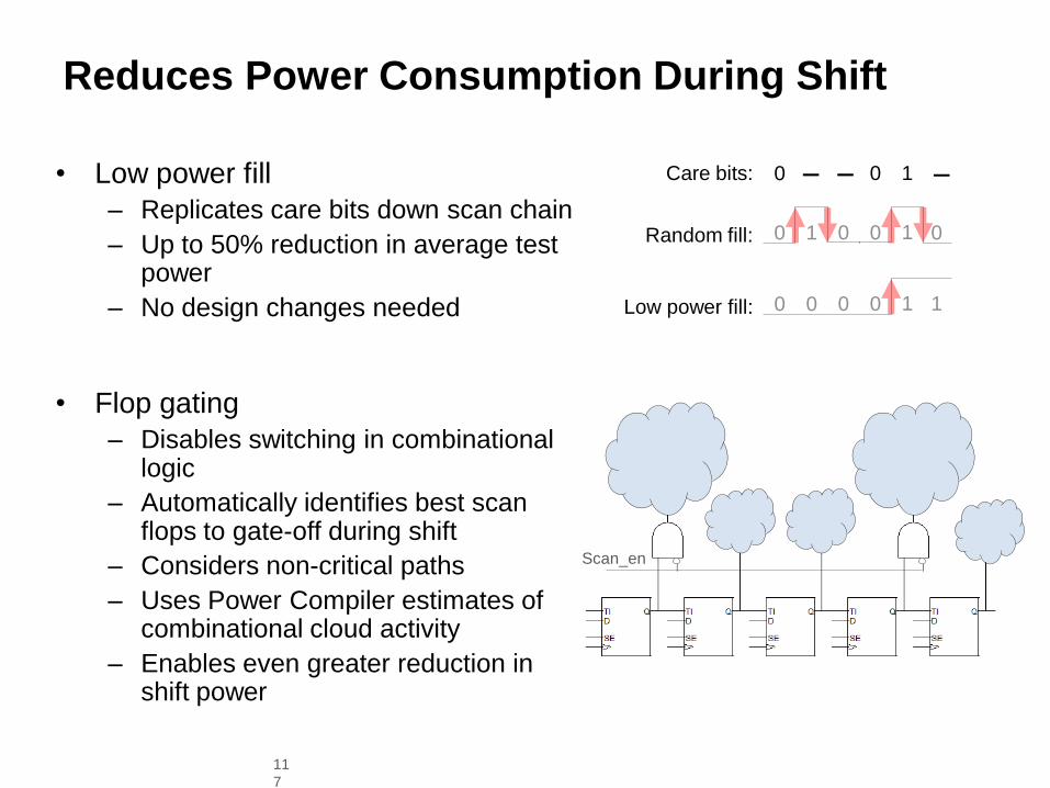
• Low power fill
– Replicates care bits down scan chain
– Up to 50% reduction in average test power
– No design changes needed
Reduces Power Consumption During Shift
• Flop gating
– Disables switching in combinationallogic
– Automatically identifies best scan flops to gate-off during shift
– Considers non-critical paths
– Uses Power Compiler estimates of combinational cloud activity
– Enables even greater reduction in shift power
Scan_en
‒ ‒Care bits: 0 10
Low power fill: 0 0 10 10
Random fill: 1 0 00 10
‒
11
8
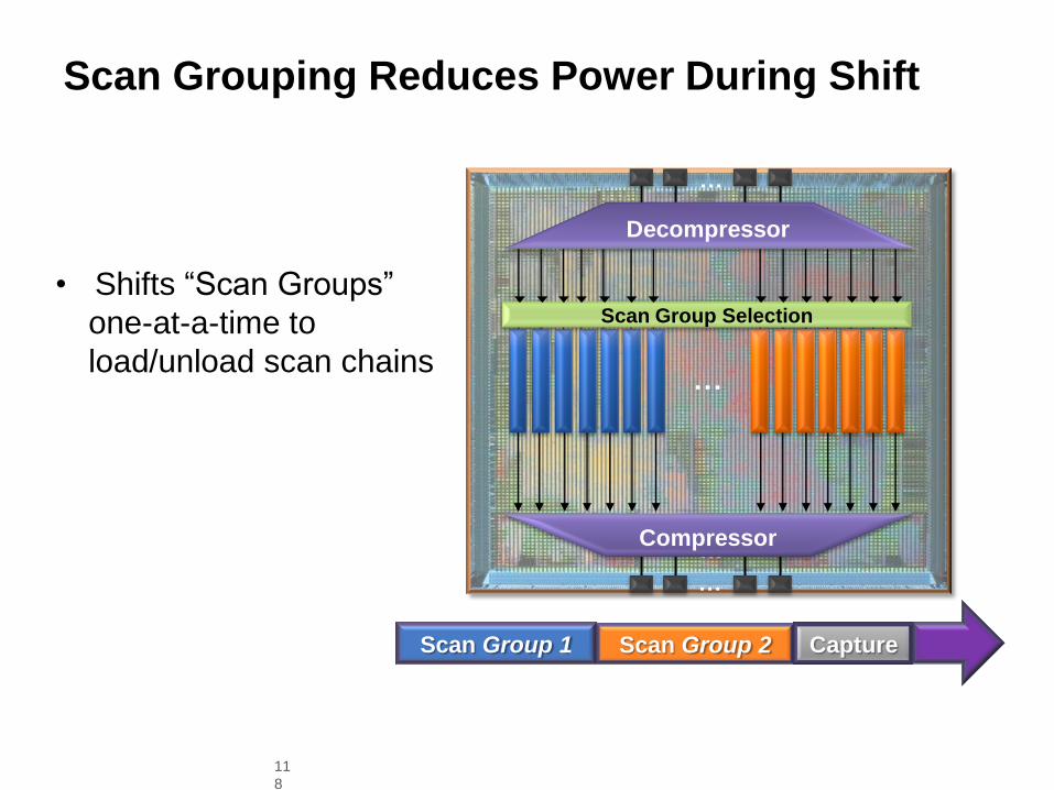
• Shifts “Scan Groups”
one-at-a-time to
load/unload scan chains
Scan Grouping Reduces Power During Shift
Scan Group 1 Scan Group 2 Capture
…
…
…
…
Decompressor
Compressor
Scan Group Selection
11
9
Minimize DFT Logic Power in Functional Mode
• Principle: gate inputs to compressor logic to block switching propagation
• Insert power-save logic that block compressor inputs during functional mode
• Minimizes area impact by leveraging compressor architecture
…
…
…
…
Decompressor
Compressor
Power-Save Logic

12
0
MPEG4 SRPG workload test-bench
MPEG XVid Player workload
• 25 frame-per-second movie
– ~ 90 second movie
– Repeats endlessly
• OLED frame buffer copy (~8ms)
– “soft” DMA decoded frame
• MPEG next-frame decode (5-15ms)
– Variable workload
– Depends on motion complexity
• OLED frame time histogram scroll (~3ms)
• Then WFI entry to chosen sleep state
– HALT (base-line leakage measurement)
– SRPG – with/without diagnostic CRC-32
Storage ’scope waveforms
SRPG Control
-IDDCPU Current

12
1
Body bias
• Body bias (for yield and/or power)
• chip vs domain,
• proc and cons (more signoff corners, bias
pg grid).
• Diminishing point in sub-40nm where sub-
threshold leakage is no longer dominate.
Gate leakage worse with body bias

12
2
90G - ARM926 CPU+CACHE - SRPG leakage
0.00
5.00
10.00
15.00
20.00
25.00
Temperature (C)
Leakag
e P
ow
er
(m
W)
CPU_SRPG(mW)
RAM_HALT(mW)
CPU_SRPG(mW) 0.10 0.10 0.12 0.14 0.17 0.22 0.29 0.37 0.51 0.68 0.94 1.22
RAM_HALT(mW) 1.27 1.65 2.23 2.90 3.82 5.01 6.46 8.30 10.7 13.8 17.4 21.1
-10 0 10 20 30 40 50 60 70 80 90 100
Leakage in temperature – TSMC90G
• Std Cell power gated (16K caches non PG)
• -10° to 100°C
1.2mW
12
3
65LP - ARM926 CPU+CACHE - SRPG leakage
0
50
100
150
200
250
300
350
400
450
500
Temperature (C)
Leakag
e P
ow
er
(uW
)
CPU_SRPG(uW)
RAM_HALT(uW)
CPU_SRPG(uW) 12 13 14 15 18 21 26 31 42 54 72 95
RAM_HALT(uW) 8 11 16 23 34 43 68 101 143 199 280 355
-10 0 10 20 30 40 50 60 70 80 90 100
Leakage in temperature – TSMC65LP
• Std Cell power gated (16K caches non PG)
• -10° to 100°C
100μW

12
4
Shaving Voltage Margins with Razor• Goal: reduce voltage margins with in-situ error detection and
correction for delay failures
• Proposed Approach:
Remove safety margins and tolerate occasional errors
Tune processor voltage based on error rate
Purposely run below critical voltage
• Data-dependent latency margins
• Trade-off: voltage power savings vs. overhead of correction
Source: David Blaauw, U. of Michigan
0.8 1.0 1.2 1.4 1.6 1.8 2.0
0
20
40
60
Supply Voltage
Perc
enta
ge E
rrors
Traditional DVS
Zero margin Sub-critical
RAZOR DVS
12
5
Razor Timing Error Detection
• Second sample of logic value used to validate earlier sample
• Need restart MEM pipeline stage after correction
Mai
n F
F
Sha
dow
Lat
ch
Mai
n F
Fclk clk
clk_del
5
49
MEM39
9
Source: David Blaauw, U. of Michigan

12
6
Considerations for production design
• Area overhead
– redundant logic, e.g. shadow latches
– Mitigation: only apply to critical paths
• Power overhead
– Dynamic and leakage power on Razor logic
– Power on recovering data where needed
• Performance degradation
– Re-do failing task or halt operation until correction
• Key design issues:
– Maintaining pipeline forward progress
– Meta-stable results in main flip-flop
– Short path impact on shadow-latch
– Recovering pipeline state after errors
– What is the “good” vdd that gives acceptable miss/hit rate?Source: David Blaauw, U. of Michigan

12
7
Main leakage currents in sub-90nm
Igate
GIDLn+n+
SG
D
• Subthreshold current
Weak inversion (OFF-state)
Increase with Vth reduction
Increase with temperature
• Gate tunneling current
High Vgs (ON-state)
Increase with Tox reduction
Dominant in sub-90nm
Not sensitive to temperature
Isub
T
VVVVgs
stsub
th
qnkT
thDS
eeII
*