
Solar Photovoltaic Installation Guidelines - City Of Beverly Hills

SAND79-7001 Unl i mited Release UC-63a· Distribution Prepared for Sandia Laboratories under Contract No. 07-6941
Design Guidelines for Large Photovoltaic Arrays
R. M. Turfier, T. J. Lambarski, R. W. Grant The 8DM Corporation

Issued by Sandia Laboratories, operated for the United States Department of Energy by Sandia Corporation .
NOTICE
This report was prepared as an account of work sponsored by the United States Government. Neither the Un ited States nor the Department of Energy, nor any of their employees, nor any of their contractors, subcontractors, or their employees, makes any warranty, express or implied, or assumes any legal liability or responsibility for the accuracy, completeness or usefulness of any information, apparatus, product or process disclosed, or represents that its use would not Infringe privately owned rights.
Printed in the United States of America
Available from National Technical Information Service U. S. Department of Commerce 5285 Port Roval Road Sf)ringfield, VA 22161
Price: Pri nted Copy $ 6 Microfiche $3.00

THE 80M CORPORATION
FOREWORD
This report, BDM/TAC-78-686-TR, is submitted by The BDM Corporation, 2600 Yale Blvd. S.E., Albuquerque, New 1·1exico 87106, to Sandia Laboratories, Albuquerque, New Mexico 87115. This report is in fulfillment of Task 3 of contract 07-6941, and presents guidelines for electrical design of photovoltaic modules and arrays for large scale applications. The program is under the direction of M. G. Semmens. The principal contributors to Task 3 were R. M. Turf1er, T. J. Lambarski and R. W. Grant.
i

THE 80M CORPORATION
Chapter
I
II
III
IV
TABLE OF CONTENTS
INTRODUCTION
A. OVERVIEW
1. Objectives 2. Background 3. Format
B. BASIC CELL OPERATION C. ILLUMINATION ENVIRONMENTS D. DESIGN PROCEDURE
INITIAL DESIGN
A. DESIGN PROCESS B. DESIGN CONSTRAINTS C. INITIAL PARALLEL STUDIES
1. Economic Analysis 2. System Analysis
D. HARDWARE DEFINITION
MODULE DESIGN AND PROTECTION
A. FAILURE MECHANISMS B. ARRAY CONDITIONS CAUSING REVERSE BIAS CELL C. REVERSE VOLTAGE PROTECTION D. THERMOMECHANICAL
1. Normal Operation Temperature Rise 2. Reverse Bias Temperature Rise 3. Forward Bias Temperature Rise 4. Heating Due to Lightning
PERFORMANCE OPTIMIZATION
A. SERIES-PARALLEL TRADE-OFFS B. BYPASS AND BLOCKING DIODE PLACEMENT
1. Bypass Diodes 2. Blocking Diodes
1-1
1-1
1-1 1-1 1-2
1-2 1-6 1-8
II-l
11-1 II-3 II-3
11-3 II-5
11-7
III-l
III-l I II-5 III-7
III-16
III-17 III-19 111-24 I II -26
IV-l
IV-l IV-6
IV-6 IV-12
C. EFFECTS OF SHORTED AND OPEN CELLS ON PERFORMANCE IV-18
THE BOM CORPORATION
TABLE OF CONTENTS (Concluded)
Chapter
1. Series Short 2. Parallel Short 3. Parallel Open 4. Series Open
REFERENCES
iii
Page
IV-19 IV-19 IV-19 IV-20
IV-23

THE 80M CORPORATION
Figure
1-1
1-2
1-3
1-4
II-l
II-2
II-3
II-4
III-l
III-2
IlI-3
III-4
III-5
III-6
III-7
III-8
III-9
III-10
III-ll
LIST OF ILLUSTRATIONS
PV Ce 11 Mode 1
PV Cell I-V Curves
Series-Parallel Trade-Offs
Design Process Block Diagram (Overview)
Initial Design Process
Enumeration of Design Constraints
Details of Initial Parallel Studies
Details of Hardware Definition
Design Flow for Module Protection
Heat Flow in a Photovoltaic Cell
One String Driving the Load with One Cell Shadowed
One Module in Reverse Bias with One Cell Shadowed
Current Through Bypass Group vs. Voltage Across Bypass Group
Voltage Across Shadowed Cell vs. Voltage Across Bypass Group
Number of Series Cells per Bypass Diode Versus Safe Reverse Cell Voltage
Current Limiting in Photovoltaic Cell Under Lightning Illumination
Simplified Model of Heat Flow in a Photovoltaic Cell
Simplified Photovoltaic Cell Electrical Model
Temperature Rise in a Reverse Biased Photocell
iv
Page
1-3
1-5
1-7
1-9
11-2
II-4
11-6
11-8
111-2
II.I-4
III-6
111-8
I II-l a
III-ll
III-13
III-15
III-18
III-20
III-23

THE 80M CORPORATION
Figure
1II-12
III-13
III-14
IV-l
IV-2
IV-3
IV-4
IV-5
IV-6
LIST OF ILLUSTRATIONS (Concluded)
Load Transient Causing Forward Bias of Photovoltaic Cells
Partial Shadowing of Parallel Photovoltaic Cells Causing Forward Bias of Shadowed Cell
Blocking Diodes Protecting the Array From Load Transients
Design Flow for Performance Optimization
Effect on Performance of Addition of Bypass Diodes for One-Cell Shadowing
Effect on Performance of Addition of Bypass Diodes for Multi-Cell Shadowing
Bypass Diodes to Reduce End Effects
Effects of Blocking Diodes on Voltage and Current
Schematic for Estimating Blocking Diode Trade-Offs
v
111-25
IlI-25
1II-27
IV-2
IV-7
IV-9
IV-ll
IV-13
IV-14

THE 80M CORPORATION
A. OVERVIEW
1. Objecti ves
CHAPTER I INTRODUCTION
The purpose of this document is to provide system design engineers with guidelines for protecting cells and obtaining optimum performance in the design of large photovoltaic arrays in normal and adverse illumination environments. Three environments are considered here: uniform illumination, selective shadowing, and illumination transients such as lightning.
Only electrical considerations are addressed in these guidelines. Economic, mechanical, civil, etc., factors are not within the scope of this contract. However, these factors are discussed briefly in Chapter II, Initial Design, and costing impacts are identified qualitatively in the protection and performance guidelines where appropriate.
The guidelines are keyed toward system design engineers who have a working knowledge of both electrical and mechanical design concepts. The guidelines provide a basic understanding of the design considerations and simple methods for estimating design tradeoffs in general cases. These methods can be applied to specific cases without computer simulation. For more exact answers to detailed questions, more complex analyses, possibly supported by computer simulation such as PV-TAP (the Photovoltaic Transient Analysis Program) (described below) may be required.
2. Background These guidelines are presented as the final product of a
contract sponsored by DOE and Sandia Laboratories to provide tools for designers and analysts of large photovoltaic arrays. Ea·rl ier phases were devoted to development of a computer code for analyzing nonlinear electrical and thermal response of photovoltaic system elements to electrical and illumination transients. PV-TAP, which resulted from this effort, is a major update of NET-2, a general purpose, nonlinear
1-1

THE BOM CORPORATION
network analysis code capable of handling a wide variety of electronic network components as well as problems arising in other engineering fields. In addition to all the capabilities of NET-2, the PV-TAP code also includes photovoltaic cells, aggregation of cells, collectors, heat transfer networks, and other PV system elements.
3. Format Introductory and background material are presented in this
chapter. The design guidelines are presented in subsequent chapters, following the three major steps employed in designing an array. The first step in designing an array is the initial design, in which design requirements, power conditioning, cell and collector selection and the basic wiring pattern are determined. The next step is design of the basic module and protection against burnout. Finally, the array is "built up" by interconnecting modules to obtain the desired power requirements in the most efficient configuration. Hand calculation techniques have been employed wherever possible, supplanted by PV-TAP runs when needed.
B. BASIC CELL OPERATION
In order to use the guidelines presented in this report, a basic understanding of photovoltaic cell operation is required. The following section details the operation of the Ebers-Moll model used in this report. Symbols and terminology will be the same throughout the report.
The photovoltaic cell is basically a PN junction diode. The behavior of the cell can be modeled with the Ebers-Moll circuit analog model shown in figure 1-1. The current source, 10, is given by the normal PN junction diode equation,
where 1ST = saturation current at a given temperature e = emission constant YO • junction voltage.
1-2

...... I
W
T(THERMAL INPUTS)
A
K
?UN (t)
Ip = LIGHT-GENERATED PHOTOCURRENT ID = STANDARD DIODE JUNCTION CURRENT CJ = JUNCTION CAPACITANCE
RSH = SHUNT RESISTANCE RS = SERIES RESISTANCE
JUNCTION RS
RSH
VD
Figure 1-1. PV ~ell Model
-I I m OJ 0 ~ ()
0 ANODE :XI
\J
+ A 0
1
:XI
- ~ IpV
0 Z
VPV
K
CATHODE

THE BOM CORPORATION
The current source, Ip' is the photocurrent generated in the junction. It can be approximated by the short circuit current, ISC ' measured at a given insolation and temperature. The photocurrent increases linearly with insolation but varies only slightly with temperature over the normal operating ranges. CJ is the junction capacitance. The shunt resistance, RSH' determines the amount of current leakage across the junction due to ohmic defects. The series resistance, RS' is a combination of the bulk resistance and resistance due to contacts.
The PV cell is operated with no external bias. When illuminated, a photocurrent, Ip' is produced across the junction as indicated in figure 1-1. This will produce a current in the external load with the positive direction as indicated. If the anode is shorted to the cathode, essentially all the current will flow through the external terminals and the output voltage will be zero. This condition is repres~nted by the short circuit current, ISC' in the typical I-V curve shown in figure 1-2. The basic shape of the curve is determined by the diode current, 10, which is exponential. When a discrete load is placed across the terminals, the voltage developed across this load biases the junction, causing some of the photocurrent to be shunted through the junction. This current, consisting mostly of 10, subtracts from the photocurrent, reducing the current available at the output.
At the other extreme is the open circuit voltage, Vac' which is obtained when the terminals are disconnected. Vac is determined by the diode equation since essentially all of the photocurrent passes through and forward biases the junction. Vac increases logarithmically with insolation since it is determined by the photocurrent, Ip' being forced through the junction as 10, Conversely, Vae decreases with temperature since the saturation current, IS' in the diode equation increases with temperature. This means that the junction is unable to sustain the same voltage at higher temperatures.
The shape of the curve in figure 1-2 is also dependent on the values of RSH and RS' These resistances cause the curve to deviate further from a rectangular shape. Small values of RSH will shunt some
1-4

THE 80M CORPORATION
I (AI~PS)
1.0
G.G
-+-----r-----r----,...------r---.,.---'-'7-i V (VOLTS)
0.1 0.2 0.3 0.4 0.5 0.6 Voe= 0.57 V
Figure I-2. PV Cell I-V Curves
I-5

THE 80M CORPORATION
of the photocurrent, reducing the current available at the output at all values of voltage. At open circuit, the current in the shunt resistor will reduce the current available to the diode equation, reducing Voe' Large values of series resistance will reduce the output voltage at all values of current. In short circuit conditions, the current through the series resistance will cause a voltage at the junction which will shunt some current through the junction elements, 10 and RSH ' This will cause Isc to be lower than the photocurrent, Ip.
The normal output from the cell described by figure 1-2 would be about 1.3 amperes at 0.45 volts. Higher voltages and currents can be obtained by placing cells in series and parallel. When identical cells are placed in series, as in figure I-3(a), the current of the string is the same as that from one cell but the voltage is the sum of the individual cell voltages. Thus, for four cells in series, the current is still 1.3 amperes, but the voltage is 4 x 0.45 = 1.8 volts.
When identical cells are connected in parallel as in figure 1-3(b), the voltage of the string is the same as that from one cell, but the current is the sum of the individual cell currents. Thus, for four cells in parallel, the voltage is 0.45 volts, but the current is 4 x 1.3 = 5.2 amperes.
c. ILLUMINATION ENVIRONMENTS
Three types of illumination are considered in this report, 1) uniform steady state, 2) nonuniform steady state, and 3) uniform transient illumination.
Uniform steady state illumination simulates normal cloudless sunlight which varies over the course of the day, but the variation is slow compared to the response time of the PV cells. Nonuniform steady state illumination represents shadowing of parts of the array by slowmoving clouds and stationary objects. Another slow illumination transient which is unique to linear parabolic trough concentrators is shadowing of cells at the en.d of a collector when the sun is low in the sky (end
1-6

THE B
OM
CO
RPO
RA
TIO
N
Vl
...J ...J I..U
U
0 I..U
:>
<:
I-
u L
rl I..U
....
N
:z
:z
0 L
rl 0 U
II
II ...J
:> -
I..U
<fj
...J I+
-...J
I+-
<:
0 c:r:
0 <
: Q
J 0
-"0
to
~
.c
I-
~
QJ ~
~
to
~
to
0-0
<fj
QJ
..... ~ QJ
Vl
M 0
-QJ ~
:::I O
l ..... I.L.
Vl
...J ...J I..U
U
<:
0 :>
I..U
M
I-
<Xl U
I..U
~
N ~
N
~ ~
:z
• :z
II
II 0 U
:>
-V
l I..U
- c:r: I..U
Vl
to
......
1-7

THE 80M CORPORATION
effects). These are considered steady state because the variations are slow compared to the response time of the PV cells.
Transient illumination consists of lightning outdoors or highspeed electronic flash simulations in a laboratory.
These illuminations can cause reverse bias and/or heating which can burn out the cells and break the connections. Shadowing and lightning can also reduce performance efficiency. These effects will be discussed in chapters III and IV.
O. DESIGN PROCEDURE
Figure 1-4 illustrates a typical procedure for designing a large photovoltaic array. In the Initial Design phase, the desired power level and terminal conditions are specified. The power cor.ditioning and load matching philosophies are chosen. Cell and collector types are chosen. An initial series-parallel wiring pattern is selected and integrated with the collector/cell types to determine an initial collector mounting configuration and collector arrangement.
Next, the basic module composed of individual cells interconnected in some basic series-parallel scheme and mounted in a package is designed and protected against burnout by the proper placement of blocking and bypass diodes.
Finally, the performance of the array is optimized by evaluating its response to various illumination conditions and making design changes as needed. The entire process is iterative. At each step, the initial design may be updated based on the results of the module protection analysis and/or array performance optimization. Each time the basic design is changed, it should be re-evaluated for burnout protection before being accepted.
Figure 1-4 is an outline of the process. In subsequent chapters, each phase is broken down and illustrated in detail.
1-8

..... I \D
SYSTEM DESIGN CONSTRAINTS
INITIAL DESIGN PROCESS
SYSTEM DESIGN CELL/COLLECTOR SELECTIOn
MODULE PROTECTION BYPASS AND BLOCKING DIODES
YES
PERFom·1MICE EVALUATION
NO
Figure 1-4. Design Process Block Diagram (Overview)
SERIES - PARALLEL PATTERN
END
-t :::I: m CD o s: ()
o :0 "'0 o :0
~ o z

THE BOM CORPORATION
CHAPTER II INITIAL DESIGN
In this chapter a typical system design process is outlined and discussed. Design constraints which influence the results and the interdependence of the various aspects of the process are also discussed. Only basic considerations of system design are addressed since the contract covers only the electrical response of PV cells and arrays.
The bibliography contains numerous documents discussing photovoltaic system design trade-offs. The designer is urged to keep abreast of the efforts in progress in the various Department of Energy "Photovoltaic Experiments" contracts awarded under the PRDA's listed in the bibliography.
A. DESIGN PROCESS
A typical Initial Design process is illustrated in figure 11-1. The process begins with an analysis of the design constraints. After these are fully specified and understood, two parallel efforts are initiated. An Economic Analysis gathers data on system components and technologies which satisfy the applicable design constraints. At the same time, generic system types which satisfy applicable design constraints are analyzed with preliminary inputs from the market survey. The results of the parallel studies are then used to reduce the number of candidate hardware combinations. These candidates are analyzed in detail before the most promising hardware are selected for the system. Finally, a series/parallel cell pattern is formulated for refinement in phases II and III of the overall design process.
The initial design phase is a complicated process and may require many iterations because of the interdependence of the results. In addition, the design may require revision based on results of phases II and III of the design process.
, II-l

THE BOM CORPORATION
SYSTEM DESIGN CONSTRAINTS
INITIAL DESIGN PROCESS I
SYSTEM ANALYSIS ECONOMIC ANALYSIS
.
HARDWARE DEFINITION
I ANALYSES OF CANDIDATE COMBINATIONS
...... SELECTION OF SPECIFIC HARDWARE (SYSTEM DESIGN, CELL/COLLECTOR)
- SELECTION OF SERIES/PARALLEL r- PATTERN
PHASES II AND III
Figure 11-1. Design Flow for Initial Design Process
II-2

THE 80M CORPORATION
B. DESIGN CONSTRAINTS
Design constraints are the key to setting up analyses and making hardware decisions. In many cases, one or more design constraints will provide clear direction and reduce the scope of the economic analysis and system analysis. Therefore, the design constraints should be clearly defined and carefully evaluated. They should also be continually referenced as criteria throughout the design process to assure applicability of the analyses being conducted and the hardware candidates being considered. Typical design contraints are listed in figure 11-2. These apply to any system being designed but will be modified, expanded and personalized for the specific-application under consideration. Some typical questions inherent in the design constraints include:
(l) Will the system output be AC or DC? (2) How much ripple or distortion will the load tolerate? (3) Will the thermal energy generated be used? (4) How much of the electrical or thermal load profile can be
economically matched with the available area? (5) Is a utility interface available at the location? (6) Are there unavoidable shadow sources? (7) Will the system be actively cooled? (8) Will the collectors be flat plate or concentrating? (9) Will the collectors be fixed or tracking?
(10) Does the statement of work specify a type of system or specific design feature?
C. INITIAL PARALLEL STUDIES
1. Economic Analysis The economic analysis provides a data base for the systems
analysis and the hardware definition activities. Data are gathered on cost, availability and performance of power conditioning equipment, collectors, PV cells, cooling systems, monitoring equipment and other
II-3

THE 8DM CORPORATION
DESIGN CONSTRAINTS
ELECTRICAL LOAD CHARACTERISTICS - TYPE AND QUALITY - LOAD PROFILE
THERMAL LOAD CHARACTERISTICS - TYPE AND QUALITY (TEMPERATURE) ,... LOAD PROFILE
GEOGRAPHIC/TOPOGRAPHIC DATA - LOCATION - AVAILABLE AREA - TERRAIN
ECONOMIC CONSTRAINTS - DESIGN FUNDS AVAILABLE - TARGET OPERATING COSTS
MISCELLANEOUS CONSTRAINTS - CONTRACTUAL - LEGAL - AESTHETIC
! SYSTEMS ANALYSIS I !ECONOMIC ANALYSIS!
-- HARD\~ARE DE FIN IT ION
~ PHASES II AND III I
Figure II-2. Enumeration of Design Constraints
II-4

THE 80M CORPORATION
related equipment which meet the design constraints previously established. Data should include expected lifetime, reliability, maintenance requirements and cost, operating specifications, size, weight, safety features and many more. Current data and conservative projections for improvements by the procurement date should be included. Only preliminary rough cut data and data of a generic nature are required for the system analysis while data for hardware analyses should be as complete as possible. (See figure 11-3.)
2. Systeni Analysis Based on the design constraints previously established, analyses
are performed on generic systems. The analyses are designed to answer . many of the questions listed above in the section on design constraints. Thus, specific hardware is not analyzed but rather general issues concerning the des irabil ity of such features as battery storage, pO\~er tracki ng, concentrating collectors, active cooling, utility interface and various cell technc10gies are addressed.
The analyses can be performed using hand techniques and computer simulation. Programs such as SOLCEL are very useful for this type of analysis. SOLCEL is a simulation program designed specifically for photovoltaic systems analysis and design optimization. Photovoltaic convers i on model ing is based upon cell parameters. Concentra t i ng, nonconcentrating. tracking and nontracking systems are available for simulation. Other subsystem models included are power conditioning, energy storage. and either utility or diesel generator backup. Total subsystem performance may be evaluated using either life cycle or levelized busbar energy costing methods. A self-contained routine allows the system performance to be optimized relative to subsystem or component sizing for a defined load and insolation data base. The program is available from Sandia Laboratories, Albuquerque, Photovoltaic Systems Definition Project Division.
The generic studies are interdependent and iterative in that the results of various analyses may provide requirements for additional generic analyses or may force repetition of previous analyses with revised inputs.
U-5

..... ..... I
0>
I DESIGN CONSTRAINTS
Ii
SYSTEMS ANALYSIS ECONOMIC ANALYSIS
1) ANALYZE BASIC PV COMBINATIONS 1) GATHER PRELIMINARY DATA
- POWER CONDITIONING - CuST - COLLECTORS - AVAILABILITY - PV CELLS - PERFORMANCE - COOLING
2) REITERATE ANALYSES 2) OBTAIN DETAILED DATA AS NEEDED - pmFORMANCE
II
M HARDI'IARE DEFINITION , Y PHASES II AND III I
Figure 11-3. Details of Initial Parallel Studies
.
-l I m OJ o ~ () o :::c '"0 o :::c ~ o z

THE 80M CORPORATION
D. HARDWARE DEFINITION
The design process for hardware definition is illustrated in figure 11-4. Based on the market survey and the generic studies, the answers to such alternatives as active versus passive cooling and flat plate versus concentrator lead to a reduction of the candidate hardware combinations under consideration. The candidate hardware combinations are analyzed with specific hardware data using hand techniques and computer simulation such as SOlCEl. Analyses are reiterated as needed to el iminate candidates whose performance i ~ not cost-effective. Deta i1 s such as collector sizing and orientation, power conditioning and energy storage design, and coolant velocity and temperature are considered.
Based on these analyses, the most promising hardware combination is chosen and analyzed to determine the optimum design parameters. Hardware selection or preliminary design options may require updating and reanalYSis. The degree of reiteration will depend on the complexity of the system and the clarity with which the design constraints are understood. Therefore, the design constraints should be continually reviewed and updated if needed.
As one of the results of these analyses, terminal conditions are specified. The voltage-current ratio determines the ratio of series to parallel connections. The cells are arranged within the collectors in a preliminary series-parallel pattern which may be revised based on results of phase II and III, Module Protection and Array Performance Optimization. The prel iminary series-parallel pattern selected may affect collector and cell design conditions and specifications such as shadow patterns, collector length and cell dimensions. These may in turn require some redesign of the prototype system.
It should be remembered throughout that many of the design steps are interdependent and changes in one design feature may produce changes 1n others.
II-7

THE 8DM CORPORATION
DESIGN CONSTRAINTS
I SYSTEMS ANALYSIS I I ECONOMIC ANALYSIS J
HARDHARE DEFINITION
1) ANALYSES OF CANDIDATE COMBIriATIONS a) Answer Questions
- ACTIVE OR PASSIVE COOLING? - FLAT PLATE OR CONCENTRATOR?
b) CHOOSE CANDIDATE COMBINATIONS c) PERFORM HARDVJARE - SPECIFIC ANALYSES d) REITERATE b) AND c) AS NEEDED
2) SELECTION OF SPECIFIC HARDWARE
-" a) CHOOSE r40ST PROtn SING HARDWARE b) PERFORM DETAILED ANALYSES c) REITERATE a) AND b) AS NEEDED
3) SELECTION OF SERIES/PARALLEL PATTERN a) DETERMINE TERMINAL CONDITIONS b) SELECT SERIES/PARALLEL RATIO c) DETERMINE COLLECTOR LENGTH AND
CELL AREA
PHASES I I AND II ~
Figure II-4. Details of Hard~lare Definition
II-a

THE 80M CORPORATION
CHAPTER III MODULE DESIGN AND PROTECTION
Once the initial design has been specified, the next step is to design the basic module. Figure 111-1 shows the Design Flow for module
design. The applicable initial design results are shown as inputs to the process. The most important design consideration is prevention of failures
due to electrical overstress (burnout) and overheating (thermomechanica1 failure). Electrical overstress is limited by careful placement of
bypass diodes to prevent cells from experiencing high reverse bias and breakdown. In a long series string, some cells can be forced into reverse
bias if they have photocurrents which are significantly lower than the
average or if they are shadowed. The degree of reverse bias is dependent to a large extent on the number of cells in series. The addition of
bypass diodes breaks up a series string into smaller series strings
reducing the maximum reverse bias attainable across any ind1vidual cell. This is discussed in more detail in subsequent sections.
The temperature rise is presented as a function of cell operating conditions and illumination conditions. To permit a general solution,
the rise is given relative to the temperature rise for ~ cell operating
at open circuit under full design illumination. It is assumed that the designer will consider the temperature rise of an open circuit cell at
full design illumination as part of the initial design.
Cost impacts are not discussed in these guidelines. However, the cost of implementing any design improvements should always be considered
and alternate methods of accomplishing the objections more economically without sacrificing cell protection should be evaluated.
A. FAILURE MECHANISMS
All of the failure mechanisms associated with the photovo1taic cell are basically the result of overheating some portion of the cell, such as
solder joints, metalization strips on the illuminated surface, or the PN
Ill-l

THE BDM CORPORATION
SERIES/PARALLEL PATIERN I
BASIC PATIERN
SHADOWING I
I
I f10DULE DESIGN MID PPOTECTION J ~ JUNCTION BURNOUT II SYSTEll DESIGN I I CELL DATA
V'" ~ lCTlVE/PASSIVEI
1 aREAKDo\iN r THERMOI·IECHANICAL FAILURE COOLl:IG VOLiAGE
• DESIGN SOLUTIONS J BYPASS aIODE PLAW1E:IT
SLaCKING DIODES
COOL ING IMPRO'lEl-lENTS
DESIGti '10 GO 9;'CK ACC£?TABLE? TO
YES
~ GO Or!
Figure 111-1. Design Flow for Module Protection
1II-2

THE BOM CORPORATION
junction. Figure 111-2 shows the heat flow in a PV cell from the edge
view. The arrows into the upper surface represent the power deposited by
the sunlight. The electrical contacts shown at the left edge may either
remove power as in the normal operating mode, or deposit power as in reverse bias operation. Under normal operating conditions, the insolation
power is uniformly deposited across the cell and the electrical power is relatively uniformly removed from the cell. The remaining heat must be
dissipated through the substrate to the heat sink as indicated by the
arrows below the cell. By contrast, however, the electrical power deposited when the cell
is operating in reverse bias can under some circumstances be deposited in
a small volume due to defects in the cell. Under these conditions of localized heating, the effective thermal resistance is greatly increased due to the small area dissipating the heat. Under normal conditions
where the heat is uniformly deposited, the effective thermal resistance
may be calculated from the cell geometry. In reverse bias when localized
heating is taking place, the effective thermal resistance cannot be accurately modeled, since it is dependent on geometric parameters which
cannot be practically determined. Therefore, two failure mechanisms will
be considered: overheating due to uniform energy deposition, and reverse bias overvoltage. Failure due to reverse bias overvoltage is said to
have occurred when the reverse bias voltage is sufficient to cause non
uniform heating and failure in some devices. The problem of uniform overheating wa~ analyzed at the individual cell level and is discussed in
section D. Reverse bias overvoltage is controlled by the module design and is discussed in sections 8 and C.
The thermal transient due to the lightning illumination pulse is
included in the cell analysis and discussed in section D. The effect of the lightning illumination transient on the worst case reverse bias cell voltage is discussed in section C.
III-3

___ I
ELECTRICAL * CONNECTION V t ....... ..... ..... I
""" POWER
TO HEAT SINK
POWER TO
* POWER REMOVED = V X I
INSOLATION pm~ER
HEAT SINK
Figure 111-2. Heat Flow in a Photovo1taic Cell
TYPICALLY 0.5 TO 3-in. DIAf1ETER
-i I m [D
o s: ()
o )J -0 o )J
~ o z
TYPICALLY 10 TO 15 x 10-3 in.

THE 80M CORPORATION
B. ARRAY CONDITIONS CAUSING REVERSE BIAS CELL
The purpose of the array analysis is to demonstrate the system response to transients and to illustrate how nonuniform transients (or
short circuit current tolerance) can cause individual bypass groups or cells to go into reverse bias operation. To illustrate how nonuniform
illumination (or short circuit current tolerance) can cause reverse bias, consider figure 111-3 which shows one string driving a load. Since all
the cells in the string are in series, the same current must flow in each cell. Under normal operating conditions and full design illumination, typical array operating voltages are in the range of 200 to 450 volts.
The ratio of peak power cell voltage (VpPC ) to open circuit cell voltage
(VOCC) is typically in the range of 0.75 to 0.85 for single crystal silicon cells at design insolation. Therefore, the open circuit string
voltage (VOCS ) is typically in the range of 235 to 600 volts. HO'Hever, the current flowing through the string reduces the operating voltage of
each cell from the open circuit cell voltage such that the operating voltage of the string is equal to the voltage of the load. If one cell is completely shadowed so that it produces no current. then there can be
no current flowing through any of the other cells (assuming the shadowed cell does not go into reverse breakdown and fail and neglecting the shunt
resistance of the shadowed cell). Therefore, all the illuminated cells
in the string are operating at
Voce or 234.3 to 599.5 volts. add up to zero; that is. 234.3
their open circuit voltage which is VOCS -However. the voltages around the loop must to 599.5 volts for the illuminated cells
minus 200 to 450 volts for the load must equal the reverse bias voltage
of the shadowed cell. Therefore. the shadowed cell would have 34.3 to
149.5 volts reverse bias. which is well above the maximum safe reverse
voltage of most cells and can be expected to cause failure. If the
shadowed cell is not completely dark. it will produce some current and> the operating conditions of the string will be somewhere between uniform illumination and complete shadowing of one cell. That is to say. the
shadowed cell will be operating somewhere between the normal operating
voltage of +0.38 to 0.6 volts and reverse voltage of 34.3 to 149.5 volts.
III-5

THE 80M CORPORATION
VOCC = OPEN CIRCUIT CELL VOLTAGE
VpPC = PEAK POWER CELL VOLTAGE
VI' = OPEN CIRCUIT uCS STRIN3 VOLTAGE
+
+
OPEN + CIRCUIT - VOLTAGE
LOAD
+ VOCS -VOCC
*: Vocc
~ 1=0 +
OPERATING VOLTAGE (AT APPROXIMATELY PEAK POWER) TYPICALLY 200 to 450 V
TYPICAL VOCC = 0.5 TO 0.7 V
VpPC Voce = 0.73 TO 0.85
Figure 111-3. One String Driving the Load with One Cell Shadowed
111-6

THE 80M CORPORATION
The maximum reverse bias voltage which can appear across any individ
ual cell is limited by placing bypass diodes around each bypass group as
shown in figure 111-4. In exactly the same manner as in the string, the
shadowed cell blocks current flow through the remaining cells in the bypass group. Therefore, the illuminated cells are operating at their
open circuit voltage. ~gain, the voltages around the loop must sum to zero. For a bypass group composed of eight cells operating at the design
temperature and fu1i design illumination, the seven illuminated cells will produce approximately 3.5 to 4.9 volts. Assuming that the bypass
group ;s reverse biased and the bypass diode is conducting the current
generated by the remaining bypass groups, the voltage across the bypass diode will be typically between 0.6 and 1.5 volts. This will limit the
reverse bias voltage across the shadowed cell to between 4.1 and 6.4
volts.
C. REVERSE VOLTAGE PROTECTION
The purpose of this analysis is to demonstrate the effect of shadow~ ing and lightning illumination transients on cell operating voltage, and
to provide guidelines for limiting reverse cell voltage to safe operating levels. As discussed in the preceding section, nonuniform illumination
can cause reverse bias cell operation, and bypass diode placement must be
chosen to limit the reverse bias voltage to within the safe operating
limits. The following sections will first provide an example illustrating cell operating voltage under various shadowing conditions and module
operating conditions. Then the relationship between the maximum number
of cells in a bypass group and the maximum safe reverse bias operating
voltage for one cell is explained under worst case module operating and illumination conditions.
In this example, a bypass group composed of eight cells is operated from short circuit through open circuit load conditions with seven cells
operating at full illumination and one cell operating at illumination
between zero and full design illumination. The module is loaded with a
111-7

THE 80M CORPORATION
N CELLS
TO OTHER BYPASS GROUPS AND LOAD
OPEN CIRCUIT VOLTAGE = (N-l) x VOCC
1=0
BYPASS DIODE + ... 0 • 6 to 1. 5 V
VOCC = OPEN CIRCUIT CELL VOLTAGE
TYPICAL VOCC = 0.5 to 0.7 V
TO OTHER BYPASS GROUPS AND LOAD
Figure 111-4. One Module in Reverse Bias with One Cell Shadowed
111-8

THE 80M CORPORATION
resistor whose value is varied to simulate various load conditions from open ci rcuit through short ci rcui t. The current from the bypass group is
shown on the vertical axis, the voltage of the bypass group on the horizontal axis in figure 111-5 with a single cell operating at 0, 25, 50,
75, and 100 percent of full design illumination represented by X, 1, 2, 3, and 4, respectively. This figure illustrates how shadowing one cell
limits the current from the whole string. As previously discussed, shadowing one cell limits the current output of the string and can result
in reverse bias of the shadowed cell. The operating voltage of the shadowed cell is shown on the vertical axis and the voltage of the bypass
group on the horizontal axis in figure 111-6. Figure 111-6 represents the same conditions as figure lII-5; that is, they have the same horizon
tal axis and the shadowed cell is operating at the same five illumination levels with the same plotting symbol representation. When all cells are
fully illuminated, as represented by the 4, the cell voltage is always positive. However, when the shadowed cell is operating at 75 percent of design illumination, as represented by the 3, it goes into reverse bias when the module voltage drops from the open circuit level of about 4.8
volts down to approximately 3.5 volts. Note that as the shadowed cell is more completely shadowed, it goes into reverse bias for module operating
voltages which are closer to the open circuit module voltage and it is
driven farther into reverse bias when the module is operating at short circuit. Further, when the shadowed cell is completely shadowed, no
current is produced and the shadowed cell remains in reverse bias for any resistive load on the module. Figure 111-6 clearly shows that the worst case reverse bias is produced by completely shadowing one cell while the
remaining cells remain at full illumination and the module is operated in
reverse bi as.
As discussed in section 111-8 and illustrated in figure 111-4, when one cell in the string is fully shadowed it produces no current and the
remaining cells operate at their full open-circuit voltage. If the bypass group is reverse biased as shown in figure 111-4, the voltages
around the loop must sum to zero as shown below.
111-9

4. 1\ ------------1-----------1 1 1 I ~~4444i.4 44 ~4 q4 ~
~ .'~ -
., .. ,.. -
7 .. ft ".'·\ll",] ~·~1"l.~"";\
1-----------1-----------1-----------1-----------1-----------1-----------1------------
4
-j 1
1 4
,
14
,I ~'.
? 4
; .. q{,
;;»11.
'4 ,. '-j
I:>',
) ';",
1 V. ) .. J,. 1.)'.
1 1 1
poOn ~~XXt~ ______ I-----------I-----------I-----------T----- ------I-----------f-----------,-----------I-----------1-----------,
/1 .. 1) 1).5 1.11
Figure III-5.
I.S ~." Z.5
VO ltage (Volts) Current Tllrough Bypass Group
).0 3., ~.o ,,·5 5.0
vs. Voltage Across Bypass Group
-f I m ro o 5: () o JJ -0 o JJ
~ o z

VI ..... ~
0 :>-
Q) en ..... <tI ..... ..... ..... ~
I 0 ~ :> ~
~
Q) U -0 OJ ;< 0 -0 <tI -'-VI
I." ------------1-----------1-----------1-----------1-----------1-----------1-----------1-----------1-----------I----------~ I I I
I • (l -
O.f-.
O.t)
-fl.f...
-I.?
-\ ."
_?4
- ~. (,
-l.h
-
44 4[,444444 ." 1 1 1 1 -
-
-
-
- ," H
" 'n ?,
" 1 -;,.?
44 4
?
~
4
?
,
x 0_0
4
1 2 .25 _5
,
It 1.444;",4 'it 1 -.?1;J1'~·
I
3 4 .75 LO(suns)
;.>";;t:..>.. I ?~;J' I I 111P'1f I 1'I(li ,
-4.? 1-----------1-----------1----------"1-----------1-----------1-----------1-----------1-----------1-----------1-----------1 n. (\ II • ., I .1')
Figure III-6.
I.C, ?5 i. II
Bypass Group Voltage (Volts) Voltage ,'Icross Shadowed Cell vs_ Voltage
'.5 b.O 4.C, s.n ,
Across ,Bypass Group
--I I m ro o s: () o :II -0 o :II
~ o z

THE 80M CORPORATION
where VR = Reverse voltage on the shadowed cell
N = Number of cells per bypass group
VOCC = Open circuit voltage of illuminated cell Vf = Forward voltage of bypass diode
The maximum safe reverse cell voltage will be different for diffferent
types of cells (5i, GaAs, etc.), different concentration ratio and different
cell manufacturers. Concentrator cells generally have a lower safe
reverse voltage ~hen flat plate cells. One cell manufacturer recommends
that some presently available concentrator cells be subjected to no more
than 5 volts reverse bias. The maximum safe reverse cell voltage must be
obtained for the particular cell being used. The relationship between the number of series cells per bypass diode
and the safe reverse cell voltage is illustrated in figure 111-7 for two
values of the bypass diode forward voltage and two values of the open-circuit
voltage. The forward voltage on the bypass diode depends on the size and
type of bypass diode, but the range of forwdrd voltages can be expected
to fall between 0.6 and 1.5 volts for most diodes. The open circuit cell
voltage (Voce) of 0.585 volt is typical of the open circuit voltage at full design illumination while 0.83 volt is typical of the open circuit
voltage for the same cell due to a lightning illumination transient of
100 suns. As discussed in the following paragraph the worst case bypass
group operating conditions coupled with a significant increase in open
circuit voltage due to high intensity lightning illumination represents a
very unlikely combination. A conservative design approach is to use the
open circuit cell voltage plus some percentage (suggest 10 to 20 percent) as a safety factor.
Heating due to lightning is discussed in detail in section III-D.
It will be shown here that lightning can produce no worse reverse bias than already considered due to shadowing, and therefore, need not be
analyzed for reverse bias failure. If lightning is to produce more
111-12

THE BOM CORPORATION
16
u.J 14 c
0 -c V1 V1 12 < 0.. >-cc co: 10 u.J 0..
V1 .-I
3 .-I u.J (..)
V1 u.J - 6 0::: I..L.J V1
1.1.. . 0 4
0::: L.LJ c:::l ::E ::) 2 z
V f (V) Voe (V)
1 0.6 0.585 2 1.5 0.585 3 0.6 0.83 4 1.5 0.83
o MAXIMUM SAFE REVERSE CELL VOLTAGE (V)
Figure III-7. Number of Series Cells per Bypass Diode Versus Safe Reverse Cell Voltage
III-13

THE 80M CORPORATION
reverse bias on a cell than normal shadowing transients, worst case
conditions must be maintained. Thus, one of the cells must be completely shadowed while the remaining cells being bypassed are completely illumin
ated and the bypass group is reverse biased. The probability of one cell
befng completely shadowed while the other cells in the bypass group are
fully illuminated by a lightning flash is dependent on the geometry of the array. However, the probability is quite low that part of a bypass
group would be brightly illuminated while the bypass group as a whole is reverse biased.
There are two major reasons for this important difference between normal illumination and lightning illumination. First, the normal illumi
nation is approximately uniform across the array while high intensity
lightning illumination would result from a very near strike. A near strike would be different distances from different parts of the array.
This range of photocurrents reduces the combined open circuit voltage of
the array. As the previous analysis showed, the difference between the open circuit array voltage and load voltage can cause reverse bias of a
bypass group only when the current produced by the bypass group is below
the current flowing in the rest of the string. Thus, the areas of the
array with low insolation will limit the current produced by the string, thereby reducing the probability of reverse biasing a bypass group in the
highly illuminated section.
The second and perhaps more important difference between normal and
lightning illumination is caused by the series resistance. At illumination levels many times the design levels, the series resistance limits
the output current. The current limiting effect is illustrated in figure
111-8 with a simplified photovoltaic cell model. Under normal illumina
tion the voltage drop across the series resistance (RS) is small and the output voltage (VOUT) is approximately equal to the junction voltage
(VJ ). However, high intensity lightning illumination produces so much
photocurrent (Ip) that even under short circuit conditions (VOUT=O), the voltage drop across the series resistance is near the open circuit cell
voltage. However, the photocurrent is much larger than the short circuit
111-14

THE 8DM CORPORATION
.... lOUT
L.....---i VJ ~tlD _1 VOUT
Ip = IpOXS S = HISOLATION
ID eVJ
= Isre
IpO ' 1ST ' e = CONSTANTS
VJ
- Vocc -lOUT = VOCC/RS (SHORT CIRCUIT, VOUT = 0) BUT, Ip » lOUT THEREFORE, I D "" I p
",
Figure 111-8. Current Limiting in Photovoltaic Cell Under Lightning Illumination
III-15

THE BOM CORPORATION
current which is limited to the junction voltage divided by the series
resistance. Therefore, most of the photocurrent generated flows through
the junction (1 0) forward biasing the junction near open circuit voltage.
For one photovo 1 tai c cell to 1 imi t the current produced by a bypass group and become reverse biased, the shadowing must be so complete that the
photocurrent produced is less than the current (lOUT) actually fl owi ng from the other cells in the bypass group which are not operating near
short circuit. For example, at 100 times design illumination, the short
circuit current typically increases by a factor of 5 to 10. Thus, a cell
with 5 to 10 percent illumination would produce a photocurrent equal to the short circuit current of the fully illuminated cells. Therefore, the
conditions which represent a reasonable worst case for normal illumination are an unlikely combination of conditions for lightning.
D. THERMOMECHANICAL
The possibility of the cell overheating and failing due to uniform power deposition is analyzed at the single cell level. Since the thermal
resistance is an important design parameter and must be selected for a particular applicatton, the results are given in terms of temperature
rise relative to the temperature rise under open circuit conditions. Open circuit was chosen for reference, because electrical power is not
flowing into or out of the cell and is independent of cell conversion efficiency. It is assumed that the temperature rise under open circuit
and full design illumination must be determined for the particular applicd
tion. Therefore, the temperature rise for other cell operating conditions are given in terms of this reference. Four operating conditions are
considered (1) normal bias, that is, open circuit through short circuit
with a resistive load, (2) reverse bias due to shadowing, (3) forward bias which would result from a load voltage higher than the open circuit
voltage of a string driving current back into the array, and (4) the transient heating due to lightning.
111-16

THE 80M CORPORATION
Before reviewing the four operating regions, consider the simplified
model of heat flow in a photovoltaic cell presented in figure 111-9.
Insolation power (S) flows into the cell at temperature (Te). Under
normal conditions electrical power (PO) flows out of the cell. Assuming
that all the heat emission mechanisms are reduced to a single thermal
resistance (RTH) and an infinite heat sink at temperature (TR), the
remaining power flows through the thermal resistance to the heat sink
producing a temperature rise (Te - TR). Under open circuit conditions
(PO = 0) and full design illumination (SR)' the temperature rise is the nominal temperature rise (~TO) given by the product of design illumination
times the thermal resistance. Failure of the cell will occur for Te at or above 360°F (45?oK) which is the melting point of solder.
1. Normal Operation Temperature Rise
Under normal operating conditions electrical power is being
removed from the cell. When the cell is operating at either open circuit
or short circuit either VOUT or lOUT are zero and the electrical power (PO) is zero. Thus, open circuit and short circuit cause a temperature rise of
AT = S x RTH or
When the cell is biased at peak power, the maximum electrical power is
removed and the electrical power is determined by the cell power conversion efficiency (E)
Po = E x S and
AT = (S - ES) RTH or
AT= ~TO x (1 - E) x S/SR
111-17

THE 80M CORPORATION
INSOLATION POWER(S)
P/V CELL TEMPERATURE (TC) P/V CELL
TC
• IVOUT
ELECTRICAL POWER (PO)
POWER TO HEATSINK
THERMAL RESISTANCE (RTH )
HEAT SINK AT REFERENCE TEMPERATURE (TR)
TC = (S - PO) x RTH + TR; Po = lOUT x VOUT
OPEN CIRCUIT TEMPERATURE RISE (toTO) AT DESIGN ILLut,lINATION (SR)
toTo = TC - TR = SR x RTH
Figure 111-9. Simplified Model of Heat Flow in a Photovoltaic Cell
III-18

THE 8DM CORPORATION
For a 13 percent cell conversion efficiency at full design illumination
the temperature rise would be 0.87 x ~TO. Since it is assumed that the
array is designed to tolerate a temperature rise of ~TO above the worst case reference temperature, no problem will be encountered in the normal
operating region, between open circuit and short circuit.
2. Reverse Bias Temperature Rise Reverse bias can be caused by shadowing as discussed in sections
Band e of this chapter. In reverse bias VOUT is negative and lOUT is positive, resulting in a negative electrical power (PO). That is the
electrical power is flowing into the cell. Two cases will be considered, first the ideal cell which has a very large shunt resistance and second a
cell with the worst case shunt resistance such that the power dissipation in the cell is maximized. As shown in figure 111-10 shunt resistance refers to the ohmic 1 eakage current of a photocell between short ci rcuit
and i'everse breakdown. Thus, the shunt resi stance descri bes the slope to
the reverse biased voltage versus current curve of a photocell, between
zero voltage and reverse breakdown. These analyses assume the photocell does not go into reverse breakdown (avalanche breakdown), since cells can
be permanently damaged by entering reverse breakdown. The design is expected to include bypass diodes as discussed in section e to limit the worst case reverse voltage.
For the ideal cell (RSHUNT is infinite) in reverse bias, but protected from reverse breakdown, the current is equal to the short
circuit current (Ise) of the shadowed cell at that illumination level. The electrical power at a constant reverse voltage (VR) is as follows:
Po = Ise VRi VR < 0
The ratio (K) of short circuit cell current divided by the peak power
cell current (Ipp) is very close to constant for single crystal silicon cells and typically varies from approximately 1.2 for flat plate cells to
1.06 for concentrator cells. Thus, electrical power can be rewritten in
terms of peak power cell voltage (Vpp ) and current Clpp) or power conversion efficiency (E) as follows:
III-19

THE 80M CORPORATION
eV. 1D = 1ST x (e J - 1)
1D 0 for V. < 0 J -
l/RSHUNT
(
VAVALANCE
RSER1ES -+ lOUT
RSHUNT i VOUT
~VOC
VOUT --.
Figure 111-10. Simplified Photovoltaic Cell Electrical Model
I II -20

THE 8DM CORPORATION
K = Ise/Ipp; for silicon 1.06 < K < 1.2
Po = KIppVR = IppVppKVR/Vpp
Vpplpp = ES
Po = ES K VR/Vpp
Thus, the temperature rise for the ideal cell in reverse bais is given by
~T = (S - PO) x R TH
~T = 5 (1 - EK VR/Vpp) x RTH
~T = ~TO x (1 - EK VR/Vpp) x S/SR
By contrast, the nonidea1 cell in reverse bias will have current
flowing due to both the photocurrent generated (Ise) and the shunt resis
tance (RSHUNT)' . Thus, the electrical power in reverse bias is as follows
where the current in the shunt resistor is VR divided by RSHUNT'
Since the reverse bias of the shadowed cell is caused by the other cells
in the series string, the combined current is limited to the short circuit current of the unshadowed cells operating at full design illumination
(S = SR)'
II 1-21

THE 8DM CORPORATION
Thus, using the same ratio (K) of short circuit cell current divided by
peak power cell current (Ipp) and power conversion efficiency (E), the
electrical power can be rewritten as follows.
K = ISC/Ipp; for silicon 1.06 < K < 1.2
VppIpp = ES
Po = KIppVR = KlppVPPVR/Vpp
Po = KESR VR/Vpp
Thus, the temperature rise for the worst case nonidea1 cell in reverse
bias is given by
AT = (S - PO) x RTH
AT = (S - KESR VR/Vpp) x RTH
AT = AT x - - KE -(
s VR ) SR Vpp
The reverse bias temperature rise for both the ideal cell and
worst case nonidea1 cell is plotted in figure 111-11 for full illumination
(S/S R = 1) on the shadowed cell and half illumination (S/S R = 0.5) on the shadowed cell. The horizontal axis represents the electrical power as a function reverse voltage normalized by the peak power voltage. The lower
set of labels for the horizontal axis represents reverse voltage in a
particular example where typical values are used for conversion efficiency,
peak power voltage and ratio of short circuit current to peak power
current. The difference between the ideal and nonideal cells is that the
current in the ideal cell is proportional to insolation on the shadowed
cell and the current in the nonideal cell is limited by the current in
the illuminated cells which is not affected by the illumination on the
III-22

THE BOM CORPORATION S/SR = 1.
S/SR = 0.5
6.0
5.0
4.0
AT ATO
3.0
2.0
1.0
________ ~------~--------+_------~--------~------~O. -5. -4. -3. -2.
EX/\!~PLE : E = 13%, K = 1.2, V PP = O. SOV (-2S.V) (-20.V) (-lS.V) (-lO.V)
E = CONVERSION EFFICIENCY K = SHORT CIRCUIT CELL CURRENT/ PEAK POWER CELL CURRENT
Vpp = PEAK POWER CELL VOLTAGE VR = REVERSE CELL VOLTAGE ,H = TEr~PERATURE RISE IN REVERSE BIAS
-1.
(-S.V)
liTO = TEMPERATURE RISE AT DESIGN ILLUMINATION AND OPEN CIRCUIT S/SR = SHADm~ED CELL ILLUMINATION/ DESIGN ILLUMINATION
Figure 111-11. Temperature Rise in a Reverse Biased Photocell I II -23
O.
(O.V)

THE 80M CORPORATION
shadowed cell. The net effect is that the slope of the temperature
versus reverse voltage curve is constant for the nonideal cell and is
proportional to the illumination on the shadowed cell for the ideal cell.
The worst case nonideal cell and the ideal cell represent the
limits on the response of a real cell. For full design illumination of
the shadowed cell (S/SR = 1) which represents the worst case illumination, both the ideal and nonideal response are represented by the same line.
Full design illumination on the shadowed cell is actually somewhat worse
than any normal case in that shadowing causes reverse bias. If the cell were fully illuminated, then it would not be reverse biased. However,
the amount of shadowing necessary to cause reverse bias has, in general,
a complicated relationship with the operating conditions of the array.
As indicated by the example in shown in figure 111-6, reverse bias can be
caused by a minor shadow (illumination of 75 percent of design illumination).
For thi s reason, the case of full illmi nat i on on the shadowed celli s
considered a reasonable worst case. Thus, the worst case relative tempera
ture rise under reverse bias can be expressed by the following:
AT = AT X (1 - KE VR ) Vpp
3. Forward Bias Temperature Rise
Forward bias operation (lOUT < 0) of a photovoltaic cell can be caused by either of two conditions. First a transient produced by the
load or electromagnetic coupling in the cables to the load can drive
current back into the array as shown in fi gure II I -12. Second shadol'ted cell(s) when connected in parallel with illuminated cells will not produce
any current and will act like a load to the illuminated cells as shown in figure III-l3.
In the case of partial shadowing in a parallel connection, the
voltage of the combination will be no more than the average open circuit
voltage of the individual cells. Thus, the current flowing in the shadowed
cell will be no more than the current flowing within a photovoltaic cell
III-24

THE 80M CORPORATION
+ LOAD; VLOAD > VOCA
••• __ ~~~ ____________________ --J
Fi gure I II - 12. Load Transient Causing Forward Bias of Photovoltaic Cells
/'" h~T' SHADOWED - ... --..-----..... -r NO R/·'AL CURRENT
Figure III-l3. Partial Shadowing of Parallel Photovoltaic Cells Causing Forward Bias of Shadowed Cell
II I -25

THE 8DM CORPORATION
under normal open circuit conditions. Since the shadowed cell is operating
below full illumination, the power dissipated in the shadowed cell is
lower than the power dissipated under open circuit and full design illumina
tion. Thus, the temperature rise in the shadowed cell will be less than
6TO' Transients from the load or induced on cables between the load
and the array may be kept out of the array by the use of blocking diodes
as. shown in figure 111-14. The blocking diodes allow the normal current to flow into the load when the load voltage is lower than the array and block transient current from flowing into the array when the load voltage
is higher than the array voltage. A voltage limiting device (such as a Zener diode, tranzorb, capacitor, etc.) would protect the blocking diode
from damage. The voltage limiting device must have a high impedance at normal operating voltages, but conduct large currents below the rated
breakdown voltage of the blocking diode. This configuration will keep
load transients from entering the array The voltage limiting device must
be chosen on the basis of the normal operating voltage and expected transient magnitude/duration.
4. Heating Due to Lightning
The effects of lightning with respect to thermomechanical burnout for a forward biased cell will be considered. It will be shown
that even for worst case, or near worst case conditions, the thermal
effects of lightning will normally not cause failure. Only when high
concentrations and high thermal resistances are used should the effects
of lightning illumination be considered in the design of the system. A lightning flash consists of several stages and lasts for
several tenths of a second. Of interest are the return strokes of high
current and short duration, the intermediate current as the trailing part
of the return stroke which is a much more slowly decaying current at a fraction of the amplitude, and the continuing current, a low level,
almost constant current of perhaps several hundred milliseconds duration.
The intermediate and continuing current mayor may not be present for any
111-26

THE 80M CORPORATION
.. '.
•••
• • • • • •
BLOCKING DIODES TRANSIENT CURRENT
VOLTAGE LIMITING DEVICE ( i.e. ZENER DIODE, TRANZORB, CAPAC nOR, ETC.)
Figure 111-14. Blocking Diodes Protecting the Array From Load Transients
II I -27
+ LOAD

THE 8DM CORPORATION
particular flash. Cianos and Pierce l have compiled data on the physical
characteristics of lightning, and have then modeled it for engineering usage. Their basic model of severe lightning will be considered here. This model closely resembles a lightning flash for which only 2 percent of lightning would be more severe. The parameters of interest for this
model are given in table 111-1.
TABLE 111-1. SEVERE LIGHTNING MODEL PARAMETERS
RETURN STROKES
INTERMEDIATE CURRENT
CONTINUING CURRENT
FINAL STAGE CONTINUING CURRENT
Current (kA)
140 PEAK
4 PEAK
0.4
0.2
Charge Transferred (Coulombs)
28
20
120
32
A relationship is needed between current and optical power per unit area for a given ground distance from the lightning stroke. According to a U.S. Air Force report2 on lightning, the potential between cloud and ground just prior to discharge is estimated to be 108 volts. Also it states that the conversion efficiency from electrical to optical power has been estimated to be 0.7 percent. Using these values and the 140 kA
as peak current for a severe lightning stroke,
1. N. Cianos and E. T. Pierce, "A Ground Lightning Environment for Engineering Usage," Technical Report 1, SRI Project 1834, Stanford Research Institute (August 1972).
2. B. N. Turman, T. B. Cummings and P. R. Oeabenderfer, "Measurement of Optical Power Radiated by Florida Lightning," United States Air Force Technical Applications Center, Report No. 76-7, p. 3 (March 8, 1976).
1II-28
THE 8DM CORPORATION
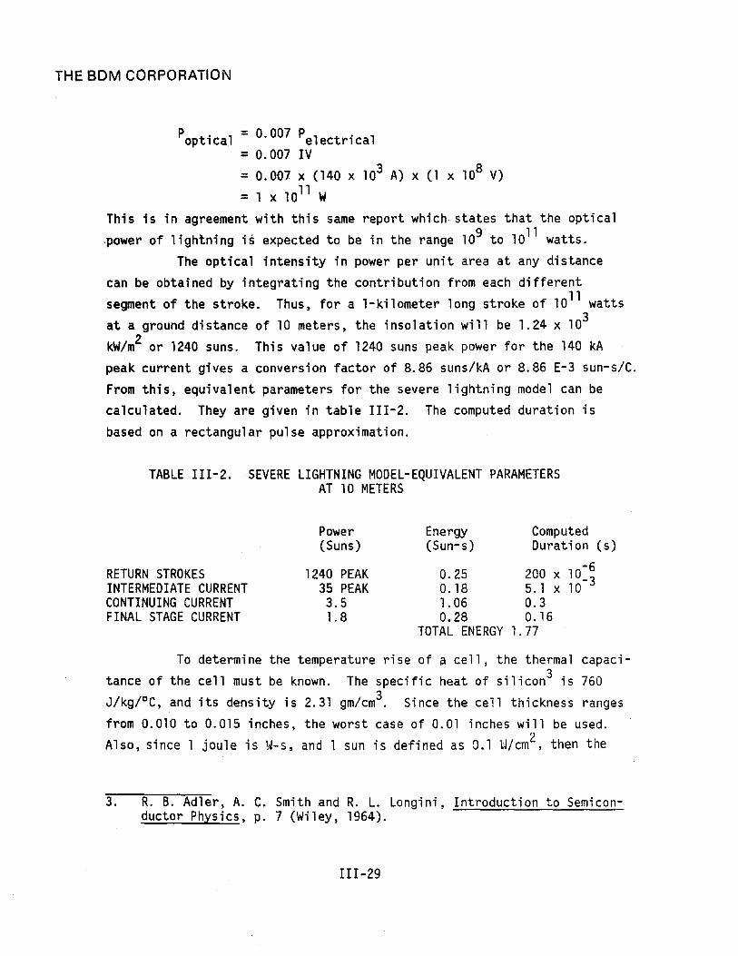
Poptical = 0.007 Pelectrical = 0.007 IV = 0.007 x (140 x 103 A) x (1 x 10⁸ V)
=lxlOll W This is in agreement with this same report which states that the optical .power of lightning is expected to be in the range 109 to lOll watts.
The optical intensity in power per unit area at any distance can be obtained by integrating the contribution from each different segment of the stroke. Thus, for a 1-ki1ometer long stroke of 1011 watts
at a ground distance of 10 meters, the insolation will be 1.24 x 10³
kW/m2 or 1240 suns. This value of 1240 suns peak power for the 140 kA peak current gives a conversion factor of 8.86 suns/kA or 8.86 E-3 sun-siC. From this, equivalent parameters for the severe lightning model can be calculated. They are given in table 111-2. The computed duration is based on a rectangular pulse approximation.
TABLE 111-2. SEVERE LIGHTNING MODEL-EQUIVALENT PARAMETERS AT 10 METERS
RETURN STROKES INTERMEDIATE CURRENT CONTINUING CURRENT FINAL STAGE CURRENT
Power (Suns)
1240 PEAK 35 PEAK 3.5 1.8
Energy (Sun-s)
Computed Duration (s)
0.25 200 x 10-~ 0.18 5.1x10-1.06 0.3 0.28 0.16
TOTAL ENERGY 1.77
To determine the temperature rise of a cell, the thermal capacitance of the cell must be known. The specific heat of si1icon3 is 760 J/kg/DC, and its density is 2.31 gm/cm3. Since the cell thickness ranges from 0.010 to 0.015 inches, the worst case of 0.01 inches will be used. Also, since 1 joule is W-s, and 1 sun ;s defined as 0.1 W/cm2, then the
3. R. B. Adler, A. C. Smith and R. L. Longini, Introduction to Semiconductor Physics, p. 7 (Wiley, 1964).
II I -29

THE BOM CORPORATION
thermal capacitance CTH can be calculated, viz.,
= 0.45 sUQ~S
The failure criteria will be a cell temperature of 455°K, the
melting point of solder. A somewhat higher temperature is required to cause failure of the bulk silicon, PN junction or meta1ization.
Initially the assumption will be used that all the energy flows
into the cell causing a temperature rise, and that none of this heat is removed, i.e., the thermal resistance to cool the cell is infinite. Then
the temperature rise, 6t, will be given by
where ES is the insolation energy in sun-so From table 111-2 the total
energy of the severe lightning flash, ES' is 1.77 sun-so This gives
This is not a sufficient temperature rise to cause failure. Now consider the case in which there is a 100X concentrator.
This increases the energy incident on the cell by a factor of 100, which
in turn increases the temperature rise by a factor of 100. The result is
a 6T of 390°C. Using a near worst case ambient temperature, TA, of
3l5°K, the temperature T of the cell is
T = TA + 6T = 315 + 390
= 705°K which is clearly a failure condition.
III-30

THE 80M CORPORATION
The assumption that the cell has no cooling is too severe for this case. However, a reasonable value of thermal resistance, RTH , from the cell to ambient conditions, can be chosen so that the temperature rise will not cause failure.
To calculate RTH , the allowed steady-state temperature increase, 8TSS ' above ambient for normal operation must be determined. Some of the trade-offs to consider are the decrease in output power and reliability as the temperature increases versus the increased cost of cooling. Since the output power is approximately proportional to the open circuit voltage,
Vac' 8TSS can be determined for any given output power degradation. Vac at 315°K is approximately 0.5 volts, and a reasonable value for the
temperature coefficent of Vae is -2 mV/oe. This gives
8TSS = 2.5°e for each 1% output power decrease. (Eq. III-l)
Because of the 100X concentrator, there will be 100 suns incident on the
cell under normal operation, giving RTH
R = 2.5°e TH 100 suns
°c = 0.025 sun for each 1% power output decrease. (Eq. lII-2)
Before considering the value of RTH to be used, the equation for 8T will be derived. The lightning will be treated a four rectangular pulses corresponding to those in table 111-2. The equivalent circuit is given here.
T
S(t)
1II-31

THE 8DM CORPORATION
where
Set) = Insolation as a function of time.
The differential equation is
set) will be considered a constant S for 0 ~ t ~ t l . The solution for AT
is
But the temperature at the beginning of each interval, TO' which defines
C1 is known.
Thus,
T = TO + (5 'TH + TA - TOJ x (1 -.-tl'THeTH) (Eq. 1II-3]
Two' cases of thermal resistance will be considered corresponding
to 10 percent and 20 percent power degradation relative to the power at
the ambient temperature. A 10 percent power degradation at 1 sun terrestial
and a concentration of 100 times give a thermal resistance of 0.25°K/sun
(using equations i11-l and 111-2). Under the same conditions, a 20
percent power degradation gives 0.50o K/sun. Evaluating equation 111-3 gives the temperature of the cell at the end of each interval of the
lightning as listed in table 111-3. The temperature for the lower thermal
resistance peaks at 43l o K for the end of the intermediate current and is
below the failure level of 455°K. The continuing current does not supply
III-32

.....
.......
....... I
W W
TABLE 111-3. CELL TEMPERATURE DURING LIGHTNING FOR TWO THERMAL RESISTANCE AND 100 X CONCENTRATION
RTH = 0.25°K/SUN RTH = 0.50o K/SUN
-I I m [II
o s: (") o :D -0 o :D
~ o z
STARTING TEMPERATURE TEMPERATURE AT END STARTING TEMPERATURE TEMPERATURE AT END LIGHTNING PHASE
RETURN STROKE INTERMEDIATE CURRENT CONTINUING CURRENT FINAL STAGE CURRENT
TO (OK) OF INTERVAL, T(OK)
340.* 395. 43l. 428.
395. 43l. 428. 395.
TO(OK) OF INTERVAL, T(OK)
365.* 420. 458. 518.
420 458. 518. 486.
*ASSUMING SUN IS SHINING, CAUSING ~T = 25°K OR 50o K, AND AMBIENT TEMPERATURE IS 315°K.

THE 80M CORPORATION
enough power to the cell to maintain the temperature and the cell begins
to cool. The higher thermal resistance does not reach peak temperature
until the end of the continuing current at 51SoK which indicates failure. These results point out that lightning will not normally cause
failure. However, for high levels of concentration and high thermal
resistance, the possibility of such failure may need to be considered
particularly in the design of the cooling system.
III-34
THE 80M CORPORATION
CHAPTER IV PERFORMANCE OPTIMIZATION
Once the basic module has been designed and protected, anc found to be compatible with the basic series parallel pattern, the next step is to optimize the performance of the array by determining the most efficient series-parallel pattern and by careful placement of blocking diodes and additional byrass diodes. Figure IV-l shows the Design Flow for performance optimization. The previous design resu~ts which act as constraints for this phase are shown as inputs to the process.
The performance optimization discussed in this chapter refers only to electrical considerations, whereas the cost of the power generated is also an important constraint. Cost trade-offs are not considered within the scope of this contract. However, areas in which costing plays an important role have been identified and the impact qualitatively addressed.
A. SERIES-PARALLEL TRADEOFFS RESULTING FROM PARAMETER VARIATIONS
Some of the factors affecting the array design with respect to series-parallel considerations are the parametric variations of the cells making up the array. These will be considered here, along with some guidelines on how to use this information in determining a reasonable series-parallel configuration. The goal is to achieve the maximum output power for the array. To do this ideally, each cell should be operated at its maximum output power point. Jhis, of course, is not possible due to the parametric variations from cell to cell.
Considering the forward biased I-V characteristics of the cells, it is the current and voltage at the maximum output power point which is of interest. These values are approximately proportional to the shortcircuit current (ISC) and open-circuit voltage (VOC ). Of interest now are the actual cell parameters which most directly affect ISC and VOC' ISC is straight-forward, because the photocurrent, Ip' is essentially
IV-l

..... <: I N
~ ~
CELL DATA
PARAMETER TOLERANCE
SERIES/PARALLEL PATTERN PERFORMANCE OPTIMIZATION ,
r-- BASIC PATTERN SERIES-PARALLEL TRADE-OFFS .l:.
SHADOWING BYPASS-BLOCKING DIODES
DESIGN YES ACCEPTABLE? END
GO BACK TO INITIAL DESIGN NO
Figure IV-l. Design Flow for Performance Optimization
I MODULE PROTECTION BYPASS DIODE
PLACmHIT
I
-i I m tIl o ~ ()
o ::xl '1J o ::xl
~ o z

THE 80M CORPORATION
identical to ISC. However, there is no parameter which is so related to
vac. It can be shown that
where
_ MKT Vac - -q- ln
IS = Saturation Current Constant in a = Temperature Coefficient in oK
P = Exponent of Temperature T = Temperature in oK M = Emission Constant
A/oKP
q/K = Electron Charge/Boltzmann Constant in °K/V Ip = Photocurrent in A
(Eq. IV-l)
Two of these variables, viz., IS and T, will be allowed to vary independently to vary Vac. (The parameter M can also vary from cell to cell, but IS and M cannot vary independently. Therefore, the data were reduced using an average value for M and only assuming varying values for IS. This technique is discussed in detail in the PV-TAP Users Guide, Vol. II, Section II-B.)
To come up with some realistic parameters, data from 4a actual cells were reduced. Using PV-TAP the parameter of interest was varied according to actual value, while the remaining parameters for each cell were all set to their average values. To check the validity of this while allowing only IS to vary, the resulting Vac distribution was compared with the actual Vac distribution of the 4a cells. They were in close agreement.
In considering the other variable, T, it can be shown that VaG versus T is nearly a linear relationship, with the resulting VaG temperature coefficient being roughly -2 mV/oG. ISC will also vary with T, but this is small compared to the variations due to Ip' and will therefore not be considered here.
IV-3

THE 80M CORPORATION
It should also be noted that Vae will vary with Ip. but this effect is small compared to IS' since the relative variation of Ip is much less than IS' (See equation IV-l.) Therefore. the effects of Ip on Voe will also be ignored here.
The approximations can then be made that
(1) Ise is only a function of Ip (Ise = Ip). (2) Vae is only a function of IS or T (equation IV-l). It is of interest now to determine which parameter will cause a
decrease in OJtput power for any particular array configuration. This decrease is defined as the difference between the maximum output power for the array and the sum of the maximum possible output powers of the individual cells. Using tile parameter values for the 40 actual cells. two arrays were considered using the PV-TAP program. These consisted of all 40 cells either in series or in parallel. The output from PV-TAP included the maximum output power for the array. with the corresponding output power for each cell. Also included was the maximum possible output power for each cell.
From these data the results given in table IV-l were derived. The value given each parameter was the average value for all cells. except the one variable parameter, which was distributed in a gaussian fashion. Its mean and standard deviation were calculated from the actual values of the 4a cells. Note that Ise distribution is the same as Ip since they are essentially the same, whereas Vae distribution is not the same as IS distribution. but is determined by the relationship as given in equation IV-l. Also note that the power degradation is essentially the same for the same relative deviation of either ISC or Vac'
The qualitative aspects of the results are what would be expected. That is, if Ise varies in a series array where the current is constrained to be the same. all cells cannot be operating at their maxlmum output power current. Li kev/i se. if Vac vari es in a para 11 e 1 array where the voltage is constrained to be the same, all cells cannot be operating at their maximum output power voltage.
IV-4
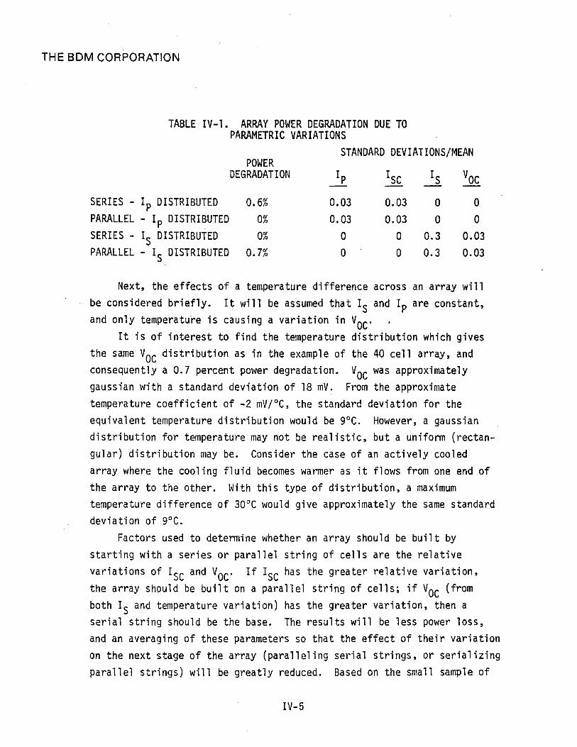
THE 8DM CORPORATION
TABLE IV-l. ARRAY POWER DEGRADATION DUE TO PARAMETRIC VARIATIONS
STANDARD DEVIATIONS/MEAN POWER
DEGRADATION Ip ISC IS VOC
SERIES - Ip DISTRIBUTED 0.6% 0.03 0.03 0 0 PARALLEL - Ip DISTRIBUTED 0% 0.03 0.03 0 0 SERIES - IS DISTRIBUTED 0% 0 0 0.3 0.03 PARALLEL - IS DISTRIBUTED 0.7% 0 0 0.3 0.03
Next, the effects of a temperature difference across an array will be considered briefly. It will be assumed that IS and Ip are constant, and only temperatu~e is causing a variation in VOC'
It is of interest to find the temperature distribution which gives the same VOC distribution as in the example of the 40 cell array, and consequently a 0.7 percent power degradation. VOC was approximately gaussian with a standard deviation of 18 mV. From the approximate temperature coefficient of -2 mV/oC, the standard deviation for the equivalent temperature distribution would be goC. However, a gaussian distribution for temperature may not be realistic, but a uniform (rectangular) distribution may be. Consider the case of an actively cooled array where the cooling fluid becomes warmer as it flows from one end of the array to the other. With this type of distribution, a maximum temperature difference of 30°C would give approximately the same standard deviation of goC.
Factors used to determine whether an array should be built by starting with a series or parallel string of cells are the relative variations of ISC and VOC' If ISC has the greater relative variation, the array should be built on a parallel string of cells; if VOC (from both IS and temperature variation) has the greater variation, then a serial string should be the base. The results will be less power loss, and an averaging of these parameters so that the effect of their variation on the next stage of the array (para 11 eli ng seri a 1 stri ngs, or seri ali zing parallel strings) will be greatly reduced. Based on the small sample of
IV-5

THE 8DM CORPORATION
Solarex flat plate cells, the power loss due to parameter variation is small for either series or parallel connection. However, a temperature gradient across a collector can increase VOC variations providing an advantage to serial connection.
In addition to these electrical trade-offs, cost can play an important role in selection of the optimum series-parallel pattern. For example, the number of bypass diodes used in the array can be reduced by using parallel connection of cells as the basic unit. The only criteria for placement of bypass diodes for cell protection is the maximum number of cells which can safely be connected in series to prevent overvoltage on a single cell. Connecting cells in parallel before serializing will not increase the cell vulnerability because the voltage is not affected by para 11 el i ng.
There are other considerations, as discussed in section IV-C for determining series-parallel wiring patterns. They all need to be considered together, in light of the objectives, to determine an optimum design.
B. BYPASS AND BLOCKING DIODE PLACEMENT
It was noted in chapter III that bypass diodes can be used for cell protection. Once the cells have been protected, additional bypass diodes can be positioned to improve performance. The additional bypass diodes reduce the detrimental effects of parameter tolerance, shadowing, and cell failure. The addition of diodes in blocking positions can also improve performance. Too many bypass and blocking diodes, however, can reduce output and cost effectiveness. The use of these diodes to optimize performance is discussed below.
1. Bypass Diodes In a given series string, shadowing of a single cell can
present an open circuit to the rest of the string. The output of the entire string can be lost. If the string contains a bypass diode, shadowi ng will cause the stri ng to go into bypass. The voltage of the string will be lost and an additional voltage drop will occur across the bypass diode. This condition is illustrated in figure IV-2(a). If more bypass diodes are used (as in b and c). the performance is improved
IV-6

THE 8DM CORPORATION
~HADOWED CELL
G-Vb
I j
t-~ VlliJ
3n 4" VAVG -Vb
I
SHADOWED t ~~ CELL
W I $ ~HADOWED
3 n· 4" VAVG
1 ~
n CELLS IN SERIES
I
t ...,Ir- BYPASS DIODE
CELL
~ VAVG --1 T
I
t
O.OV ...... __ --' o .OV
I ~
~ t-
n 4" VAVG
r
I
t -; ~
I
1 ~
I
t -; ~
1
I
t -: Ir-
o .OV
(a) One Bypass Diode (b) TriO Bypass Di odes (c) Four Bypass Diodes
Figure IV-2. Effect on Performance of Addition of Bypass Diodes for One-Cell Shadowing
IV-7

THE 80M CORPORATION
because less and less of the string is in bypass. The voltage of the string. VS' will be the average voltage per cell times the number of cells in series minus the number of cells bypassed minus one bypass diode voltage drop.
where n = number of series cells m = number of bypass diodes VAVG = average voltage per cell Vb = bypass diode forward voltage
It would appear from this scheme that the optimum situation would be to bypass every cell. This is not correct. In addition to the obvious cost penalty of implementing so many bypass diodes, consider the condition illustrated in figure IV-3 in which more than one cell is shadowed. For n/3 cells shadowed in a single bypass group, the results are the same as in figure IV-2(a). The improvement in splitting the string into two bypass groups is the same as in figure IV-2(b). Increasing the number of bypass groups to four does not yield any improvement; rather, it reduces the voltage by another bypass diode voltage drop. The general equation for the voltage as a function of the number of cells shadowed and the number of evenly spaced bypass diodes is
Vs = m - ROU~DUP(fm) nVAVG
- ROUNDUP(fm) x Vb
where m n
f
ROUNDUP(fm) fn
fm = nlm
ROUNDUP VAVG Vb
= number of evenly spaced bypass diodes = number of cells in series = fraction of cells shadowed = number of bypass groups in bypass condition = number of cells shadowed divided by number of
cells in each bypass group = increase to next higher integer = average voltage per cell = bypass diode forward voltage drop
IV-8

THE 80M CORPORATION
O.OV ~--~ O.OV O.OV .------'
(a) One Bypass Diode (b) Two Bypass Diodes (c) Four Bypass Diodes
Figure IV-3. Effect on Performance of Addition of Bypass Diodes for t1ulti-Cell Shadowing
IV-9

THE 80M CORPORATION
Very little can be said about optimizing the design against random shadowing. If distributions of shadow sizes due to clouds, airplanes or other causes can be generated. an optimum spacing may be calculable. This would at best be a tedious task and at worst would not provide any significant improvement. The prjme concern might well be the cost of implementing bypass diodes beyond the number required for protection.
For recurrent shadows, such as might be caused by collector end effects or nearby structures, maximum efficiency would generally be obtained by spacing bypass diodes so that no more than one bypass group is in bypass due to the shadow. In some cases, it might be desirable to deviate from even spacing in such a manner that extra bypass diodes are used only across those cells that are shadowed. Consider an example in which protection criteria require bypass diodes every 20 cells, but up to eight cells of some strings are shadowed due to a nearby structure. It would then be desireable to bypass the last eight cells in each of these strings with one or two' diodes depending on the propagation pattern of the shadow and the cost per efficiency improvement of implementing these diodes.
where n f
The voltage obtained using this type of bypass scheme would be
= number of cells in series string = fraction of cells in shadow
VAVG = average voltage per cell m = number of bypass diodes in shadowed group Vb = forward voltage drop of bypass diode
In the case of collector end effects (as illustrated in figure IV-4, bypass diodes could be used to improve efficiency during end shadowing. However, the cost of the additional diodes beyond the number required for protection must be weighed against the impact of removing PV cells from the ends of the receiver tube or of lengthening the parabolic trough to reduce end effects.
IV-10

TH
E 8
0M
CO
RP
OR
AT
ION
" " " " V
l oj.J U
<II 4
-
" 4
-U
J
" "0
C
" U
J
" <II
/ u ::l
/ "0
<II
/ 0
::
/ 0
....,
" V
l <II "0
0 .~
a Vl
Vl
to a. >
, <
C
<:j' I
>
...... OJ ~
::l C
'l .~
L.o..
IV-ll

THE 80M CORPORATION
2. Blocking Diodes When series-connected strings of cells or modules are
paralleled, blocking diodes can sometimes be used to improve performance. The blocking diode may be useful when several cells in a series string are shadowed (as illustrated in figure IV-S). Not only does this string produce no output, but if no blocking diodes are used, this string could also drain some of the current from the other strings, further reducing the current and voltage to the load. If blocking diodes are used, the loss may be reduced because no current can flow into the unproductive string. The output voltage will be reduced, however, by the forward voltage drop of the blocking diode in each string. This voltage loss occurs under normal operation. Therefore, any improvement in performance during shadowing could be offset by the loss in performance during normal operation. Even during shadowing, the losses due to blocking diodes could be greater than the loss without blocking diodes. A rough estimate of the trade-off in using blocking diodes is derived below.
Some assumptions and limitations should first be considered. (1) Since blocking diodes are in series with the PV cells and the
forward voltage subtracts from the voltage of the cells, the voltage of the cells in series, VS' must be much greater than the forward voltage, Vf , of the blocking diodes. Thus, for n cells in series,
Vs = n VMP » Vf
where VMP is the voltage of the individual cells at the maximum (peak) power point. It should be obvious that if the basic array building block is composed of parallel-connected PV cells. blocking diodes cannot be used in the basic module.
(2) Blocking diodes are placed on series strings when they are paralleled. But then, the subarray consisting of paralleled strings may be connected in series with other similarly connected subarrays (as illustrated in figure IV-6). There are n cells
IV-12

THE 8DM CORPORATION
SHADOlIED
Sl
( E 1141'i) - lORAIN i-2 -------. ..... -;------ ----
r--1_+--,II~P2 r--1r--,
S2 51'!
'--------'--- - - - - - - - -(a) No Blocking Diodes
<i:. I:~pj) \1 2 2 -
l...--___ --" ____________ '--__ ____
(b) With Bl acki ng Diodes
Figure IV-5. Effects of Blocking Diodes on Voltage and Current
IV -1.3

THE 80M CORPORATION
Pl
SHADmJ£D STRING
P2
k SUBARRAYS
Pk
r__---.....---..... - - - - - - ., Sm
n - - - - - - -~ERIE~
. ~ELLS
_____ .J
Figure IV-6. Schematic for Estimating Blocking Diode Trade-offs
IV-14
m PARALLEL STRINGS

THE 80M CORPORATION
in series, m strings in parallel and k subarrays in series. If one string is shadowed, the whole subarray, P1, could become reverse-biased, since in this condition the subarray is similar to a single cell in a series string whose Ip value is lower than the rest. If the subarray is reverse-biased, the blocking diode is not needed. Thus, for the blocking diode to be useful, the subarray must remain forward-biased. This can only be achieved if the short circuit current of the remaining m-1 strings, (m-1) ISC ' is greater than the normal peak power current, IMP' of the other subarrays. Thus, (m-l)I SC ':' mI MP ' Since IMP ~ 0.9 ISC '
0.9
Therefore, m .:. 10. Actually, m must be even greater than this since the voltage of the subarray must be not only nonnegative but greater than Vf .
(3) Current will not be drained from the m-1 strings into the shadowed string and thus, no blocking diode needed,un1ess the subarray voltage, Vp1 ' remains greater than the voltage of the shadowed string, VS1 ' Since the unshadowed cells in the shadowed string will be forced into open circuit, their combined voltage, VOCS ' must be less than the voltage of the other unshadowed strings, VS'
Since VMP ~ 0.8 VOC for a given cell, the number of shadowed cells in the string, nsh ' is given by
IV-15

THE BOM CORPORATION
nsh > 0.2 n
Therefore. at least 20 percent of the cells must be shadowed. Actually. more than this must be shadowed since the voltage of the subarray will drop below nVMp • With these assumptions in mind. consider the schematics in
figure IV-S. With no blocking diodes, the power lost during shadowing will be the loss of string Sl plus the power lost from the other strings into Sl. In a worst case situation, the voltage of Pl remains at nVMP while all of Sl is shadowed. To induce a voltage on Sl of nVMP ' an amount of current equal to the short circuit current minus the peak power current of one string must be forced through the shadowed string. Therefore, the power lost without blocking diodes is given by
With blocking diodes, the power lost during shadowing will be the loss of the string Sl plus the loss due to using blocking diodes in Pl and all the other k-l subarrays.
To guarantee the usefulness of blocking diodes
Substituting the expressions and eliminating the identical first terms in each yields
IV-16

THE 80M CORPORATION
Since, IMP 0.9 ISC
Eliminating IMP from both sides of the equation and assuming Vf~VMP' which is generally' optimistic.
n > 9(mk - 1)
For m = 10 or 11, the number of cells in each string which determines the ratio VS/Vf is given for k subarrays in series in table IV-2.
k
TABLE IV-2. NUMBER OF CELLS REQUIRED IN SERIES STRING VERSUS NUMBER OF SUBARRAYS
n m = 10 11
= 2 171 189 3 261 288 4 351 387 5 441 486
Since this is a conservative estimate of n, it can be seen that blocking diodes are only marginally useful for k > 1 and then only for m > 10 and n > the values shown.
The condition k = 1 occurs when the total array is completed by connecting subarrays in parallel. This case is not covered by the above table since the condition m ~ 10 was specified based on k > 2. In this case, the expression reduces to the following.
n > 9 (m - 1)
IV-17

THE 8DM CORPORATION
To illustrate the significance of these expressions consider two examples. For both examples, assume the output voltage of the array is at a particular level within the typical range of 200 V to 450 V. The first example uses f1ate plate cells with peak power at 1 amp and 0.5 volts. Thus, for a 100 kW array, the ratio of n divided b.y m is between 0.8 (400/500) at 200 V and 4.1 (900/220) at 450 V. For larger arrays the ratio would be lower. Therefore, since n < 9 (m - 1), even with k = 1, blocking diodes would never improve performance. However, blocking diodes may be required for protectlon.
The second example uses concentrator cells with peak power at 40 A and 0.5 V. Thus, for a 100 kH array with k = 1, the ratio of n divided by m is between 32 at 200 V and 163 at 450 V. Therefore, for high currents per string or multiple strings per blocking diode, blocking diodes can under certain shadow conditions improve performance. However, the losses due to blocking diodes are present all the time, but the conditions where performance is improved by blocking diodes is intermittent. Therefore, the user must evaluate the efficiency of using blocking diodes for performance improvement for his particular case. If, for example, the final aggregation consists of paralleling (k = 1), and m is small (e.g., 4 strings), then, the use of blocking diodes (in this case, only 4) is certainly warranted.
C. EFFECTS OF SHORTED AND OPEN CELLS ON PERFORMANCE
When a cell fails either short or open, the power output of that cell is lost. The failure can sometimes cause greater losses, however, than just the power of the one cell. The amount of power loss depends on the method of connection of the cell and the placement of bypass diodes. Since there are two possible interconnection methods for individ-ua1 cells, series or parallel, four conditions must be considered. The power loss for each condition is outlined in table IV-3. Each will be discussed in turn.
IV-1B

THE 80M CORPORATION
TABLE IV-3. POWER LOSS DUE TO SHORTED AND OPEN CELLS
CELL CONDITION
INTERCONN ECTI ON SHORTED OPEN
SERIES LOSE POWER LOSE POWER OF OF CELL SERIES STRING
PARALLEL LOSE POWER OF LOSE POWER PARALLEL STRING OF CELL
1. Seri es Short When a series-connected cell fails short, the power loss of
the series string is only the power of the one cell because it is the same as bypassing the cell with a wire. "The voltage is lost but current will still flow.
If the series string is in turn connected in parallel with other seri es strings, there wi 11 be a s 1 i ght decrease in the output voltage of the parallel combination due to the lower voltage of the stri ng with the shorted cell. The overa 11 effect is a power loss of about one cell.
2. Parallel Short When a parallel-connected cell fails short, the power of the
entire parallel string is lost because no voltage can be maintained across the terminals.
If the parallel string is, in turn, connected in series with other parallel strings, the output voltage of the series combination will be decreased by the voltage of one cell. The situation is similar to a shorted cell in a series string except that the power loss is greater because the current is greater by the number of cells in parallel.
3. Parallel Open When a parallel connected cell fails open, the power loss of
the parallel string is only the power of one cell because it is the same
IV-19

THE 80M CORPORATION
as removing the cell or putting a blocking diode in series with a shadowed cell. No current is produced, but no current is drained from the other cells either.
If the parallel string is, in turn, connected in series with other parallel strings, the parallel string with the open cell will act like a series-connected cell that has a low photocurrent or is partially shadowed. The parallel string with the open cell could go into reverse bias. If it were part of a bypass group, the group could go into bypass. Thus, the power of the whole bypass group could be lost.
4. Series Open When a series connected cell fails open, the power of the
whole string (or bypass group) is lost because no current can be drawn from that string (or no voltage will be generated by the group in bypass).
If the series string is, in turn, connected in parallel with other series strings, the open string will have the same effect as if it were removed or as if a blocking diode were placed in a shadowed string. The situation is similar to an open cell connected in a parallel string except that the power lost is greater because the voltage is greater by the number of cells in series.
If the open string has bypass groups within it, the effect when the string is paralleled will be different. The string will not look like a"n open circuit because the bypass group with the open cell will be in bypass. The effect will be similar to the series string connected in parallel (described in paragraph 1) except that instead of losing one cell, one whole bypass group is lost plus the power lost in the bypass diode.
The effects of shorted and open cells on higher orders of aggregation can be deduced based on these guidelines.
The relative performance merits of series or parallel connection of cells in the cases of shorted or open cells can be summarized
IV-20

THE 80M CORPORATION
as follows: In the case of shorts, series-connection of cells is more desireable since only the one cell is lost whereas shorts in parallelconnected cells cause the loss of the whole parallel string.
In the case of opens, there is also an advantage to series over parallel connection of cells. In the case of series connections, opens can cause the loss of a whole string or bypass group, but in the case of parallel connections, opens can sometimes cause the parallel string to go into reverse bias and the series bypass group of which the parallel string ;s a part to experience large voltage losses or go into bypass. The relative severity of the two cases is dependent on the number of cells in parallel and the number of parallel strings in series
. per bypass group. The trade-off can be evaluated by considering the power loss for each case.
If n cells are connected in parallel, the lowest loss will occur if a bypass diode is placed across each parallel string. Thus, the loss would be limited to the single string power plus the bypass diode power.
where PLPS = power loss of parallel string VMP = voltage of cell at maximum power point
IMP = current of ce 11 at maximum power point n = number of cells in parallel
Vb = forward voltage of bypass diode If m cells are connected in series within a bypass diode, the
power lost if one cell opened would be
PLSS = (mVMP ) IMP + Vb IMP
= IMP (mVMP + Vb)
IV-21

THE 80M CORPORATION
where PLSS = power loss of series string m = number of cells in series
and other variables are as defined above. If parallel connection of cells is to be more advantageous
than series connection,
PLPS < PLSS
nI MP (VMP + Vb ) < IMP (mVMP + Vb )
For a typical case, if m = 10, VMP = O.SV and Vb = 1.OV, n must be less than 4 cells. Therefore, more bypass diodes must be used for paralleling cells than for cells in series to equalize the power losses for each case.
Therefore, by serializing cells, power loss is minimized in the case of shorted cells and cost of bypass diodes is minimized in the case of open cells. Furthermore, based on limited data, cell failures tend to be dominated by short circuits rather than open circuits.
IV-22

THE 80M CORPORATION
B I BLI OGRAPHY
1. Adler, R. B., A. C. Smith, and R. L. Longini. Introduction to Semiconductor Physics, Wiley, 1964.
2. Bell, C. R. Assessment of a Solar Photovoltaic Power Conversion System for Control Station Application, EM342-294(900-702), Jet Propulsion Lab, Pasadena, Cal., June 1975.
3. Burgess, E. L. "Photovoltaic Energy Conversion Using Concentrating Sunlight," in Proceedings of the Activity of Photo-Optical Instrumentation Engineers, Vol. 85, August 1976.
4. Cianos, N., and E. T. Pierce. A Ground Lightning Environment for Engineering Usage, Technical Report 1, SRI Project ]834, Stanford Research Institute, August 1972.
5. DOE 76-161, Photovoltaic Conversion Program - Summary Report, Department of Energy, November 1976.
6. DOE. National Photovoltaic Program-Program Plan, Department of Energy, Div;son of Solar Technology, February 3, 1978.
7. Lambarski, T. J., et al. Photovo1taic Transient Analysis Program, User's Guide, SAND73-7038, BDM Corporation for Sandia Laboratories, 4 Volumes, October 1978.
8. Linn, J. K. Photovoltaic System Analysis Program-SOLCEL, SAND77-1268, Sandia Laboratories, August 1977.
9. PRDA EG-78-D-04-0035-So1ar, Photovo1taic Concentration A 1ication Experiments, Program Research and Development Announcement PRDA, Department of Energy, Albuquerque Operations Office, January 1978.
10. PRDA EM-78-D-04-0038, Solar Photovo1taic Flat Panel A lications Experiments, Program Research and Development nnouncement PRDA), Department of Energy, Albuquerque Operations Office, May 1978.
11. Sandia Laboratories Specification 13-0308, Request for Technical Proposals to Develop Novel Designs for Low Cost Photovoltaic Concentration Arrays, Photovo1taic Systems Definition Project, Sandia Laboratories, June 1978.
12. Schueler, D. G., et a1. "Integration of Photovoltaic and SolarThermal Energy Conversion Systems," in Conference Record of Elements IEEE Photovoltaic Specialist Conference, May 1975.
IV-23
THE 80M CORPORATION
BIBLIOGRAPHY (Continued)
'13. Turman. B. N., T. B. Cummings, and P. R. Deabenderfer. Measurement of Optical Power Radiated by Florida Lightning, Report No. 76-7, Air Force Technical Application Center, March 8, 1976.
14. Wolf, M. "Performance Analyses of Combined Heating and Photovoltaic Power Systems for Resideness~ in Energy Conversion, Vol. 16, 1976.
IV-24

DISTRIBUTION: TID-4500-R66, UC-63a (269)
U.S. Department of Energy (6) 20 Massachusetts NW Washington, DC 20545 Attn: H. Harvin, Acting Deputy
Program Director Solar, Geothermal, Electric,
and Storage Systems
Division of Solar Technology (3) U.S. Department of Energy 600 E Street NW Washington, DC 20545 Attn: P. Maycock, Ass't Director
for Photovoltaics L. Hagid, Systems and
Applications Photovoltaics R. San Martin
U.S. Department of Energy (2) Albuquerque Operations Office Albuquerque, NM 87115 Attn: D. K. Nowlin, Director
Special Programs Division
SERI, Library (2) 1536 Cole Blvd., Bldg. #4 Golden, CO 80401
Jet Propulsion Laboratory (9) 4800 Oak Grove Drive Pasadena, CA 91103 Attn: R. Forney, W. Callaqhan,
J. P,rnett, R. Ross, R. Ferber, J. Fortenberg, L. Dumas, P. Sutton, R: Weaver
NASA/LeRC (3) 21000 Brookpark Road Cleveland, OH 44135 Attn: R. Palmer
A. Ratajczak R. Pickrell
Mission Research Corp. 1400 San Mateo, SE Albuquerque, NM 87108 Attn: J. Hamm
Mi.tre Corporation 1820 Dolly Madison Blvd. McLean, VA 22101 Attn: A. Cherdak
The Aerospace Corporation (2) P. O. Box 92957 Los Angeles, CA 90009 Attn: S. Leonard
B. Siegel
Arizona State University Tempe, AZ 85281 Attn: D. Evans
MIT-Lincoln Lab (4) Box 73 Lexington, MA 02173 Attn: M. Pope, R. Matlin
S. Sacco, S. Foreman
MIT - Energy Lab Cambridge, MA 02139 Attn: R. Tabors
Acurex Corporation 485 Clyde Avenue Mountain View, CA 94042 Attn: W. Masters
BDM Corporatiorl 7915 Jones Branch Drive McLean, VA 22101 Attn: J. C. Belote
Battelle Memorial Institute Columbus Laboratories 505 King Avenue Columbus, Oil 43201 Attn: D. C. Carmichael
General Electric Co. P. O. Box 8661 Philadelphia, PA 19101 Attn: N. F. Shepard, Jr.
Gilbert Associates, Inc. p. O. Box 1498 Reading, PA 19603 Attn: A. J. Sattolo
Lea County Electric Cooperative Drawer 1447 Lovington, NM 88260 Attn: 11. R. James
A. D. Little, Inc. Acorn Park Cambridge, MA 02140 Attn: 1'1. p. Teagan

DISTRIBUTION (cont)
Lockheed Nissiles & Space Co. 3251 Hanover Street Palo Alto, CA 94304 Attn: M. McCargo
Mobil Tyco Solar Energy Corp. 16 Hickory Drive Waltham, MA 02154 Attn: J. R. Wood
New Mexico State University New Nexico Solar Energy Inst. Box 350L Las Cruces, NM 88003 Attn: H. S. Zwibel
Science Applications, Inc. 8400 Westpark Drive McLean, VA 22101 Attn: Y. Gupta
Solar Power Corporation 20 Cabot Rd. Woburn, MA 01801 Attn: R. R. Addiss
Arizona Public Service Co. 411 North Central Avenue Phoenix, AZ 85036 Attn: E. R. Weber
The BDM corporation Technology Applications center 2600 Yale Blvd., SE Albuquerque, NM 87106 Attn: hi. R. Kauffman
Office of the Governor P. O. Box 41089 Minillas Stn Santurcc, PR 00940 Attn: F. Castellon
E-Sys tems, Inc. Energy Technology Center P. O. Box 6118 Dallas, TX 75222 Attn: M. J. O'Neill
General Electric Company Space Systems Operations P. O. Box 8661 Philadelphia, PA 19101 Attn: A. S. Kirpich
Intertechnology/Solar Corporation
100 Main Street Warrenton, VA 22186 Attn: H. IJiers
IV-26
-trU.S. Government Printing Office: 1979 -677-014/504
Kaman Sciences Corporation 1500 Garden of the Gods Road P. O. Box 7463 Colorado Springs, CO 80933 Attn: D. M. Jardine
Department of Water & Power City of Los Angeles P. O. Box 111 Los Angeles, CA 90051 Attn: F. R. Goodman, Jr.
Martin Marietta Corporation Denver Division Box 179 Denver, CO 80201 Attn: R. L. Donovan
Research Triangle Institute P. O. Box 12194 Research Triangle Park, NC 27709 Attn: R. M. Burge~
Solarex Corporation 1335 Piccard Drive Rockville, MD 20850 Attn: R. C. Hamilton
Sun Trac Corporation Subsidiary of OPTO Technology, Inc. 1674 South hlolf Road Wheeling, IL 60090 Attn, E. Moeller
Center for Energy Research Texas Tech University Lubbock, TX 79409 Attn: hi. M. Marcy
Varian Associates, Inc. 611 Hansen Way Palo Alto, CA 94303 Attn: H. J. R. Maget
Westinghouse Electric Corporation 1310 Beulah Road Pittsburgh, PA 15235 Attn: P. F. Pittman
4719 C. B. Rogers (50 ) 8266 E. A. Aas 3141 T. L. Werner (5) 3151 Iv. L. Garner (3)
For: DOE/TIC (Unlimited Release)