DESIGN GUIDE TDADP-SIL-USBC-65W-RD Description SZ1130 …
28
DESIGN GUIDE TDADP-SIL-USBC-65W-RD Description The TDADP-SIL-USBC-65W-RD reference design board describes a 65 W universal input offline power supply with programmable output voltage (5 V/3 A, 9 V/3 A, 15 V/3 A, 20 V/3.25 A). The power supply uses SZ1130 (Flyback PWM controller with integrated active clamp circuit) IC, Transphorm TP65H300G4LSG (650 V SuperGaN ® FET) and Weltrend WT6633P USB PD controller. This design shows the high-power density and efficiency that can be achieved due to the high level of integration of the SZ1130 controller. This document contains the power supply specification, schematic, bill-of-materials, transformer documentation, printed circuit layout, and performance data. Key Specs Schematics Input 90-265 Vac Output Voltages 5 V, 9 V, 15 V, 20 V Max Output Current 3.25 A Max Output Power 65 W Output Port USB-C PD Efficiency >94% Full Power Efficiency SZ1130 Features ▪ Integrated High Voltage Active Clamp FET, Active Clamp Driver, and Start-up Regulator ▪ Capable of Over 94% Efficiency ▪ Flat Efficiency Across Universal (90-265 VAC) Input Voltage and Load ▪ Tight Switching Frequency Regulation for Improved Input EMI Filter Utilization ▪ Up to 140 kHz Switching Frequency Operation ▪ OptiMode TM Cycle-by-Cycle Adaptive Digital Control ▪ Multi-Mode Operation (Burst Mode, Quasi- Resonant, Valley Mode Switching) ▪ Advanced Valley Mode Switching for low EMI ▪ Self-Tuning Valley Detection ▪ OTP, UVLO, OVLO, PCL, OPP and OSC Protections ▪ <50mW No Load Power Consumption of the IC ▪ Up to 65 W Output Power Applications ▪ High-Power-Density USB-PD AC/DC Power Supplies May 01, 2021 Silanna Semiconductor and Transphorm Page 1 tdadp-sil-usbc-65w-rd-ov1
Transcript of DESIGN GUIDE TDADP-SIL-USBC-65W-RD Description SZ1130 …
DESIGN GUIDE TDADP-SIL-USBC-65W-RD
Description The TDADP-SIL-USBC-65W-RD reference design board describes a 65 W universal input offline power supply with programmable output voltage (5 V/3 A, 9 V/3 A, 15 V/3 A, 20 V/3.25 A). The power supply uses SZ1130 (Flyback PWM controller with integrated active clamp circuit) IC, Transphorm TP65H300G4LSG (650 V SuperGaN® FET) and Weltrend WT6633P USB PD controller. This design shows the high-power density and efficiency that can be achieved due to the high level of integration of the SZ1130 controller.
This document contains the power supply specification, schematic, bill-of-materials, transformer documentation, printed circuit layout, and performance data.
Key Specs Schematics Input 90-265 VacOutput Voltages 5 V, 9 V, 15 V, 20 V Max Output Current 3.25 A Max Output Power 65 W Output Port USB-C PD Efficiency >94% Full Power Efficiency
SZ1130 Features Integrated High Voltage Active Clamp FET,
Active Clamp Driver, and Start-up Regulator Capable of Over 94% Efficiency Flat Efficiency Across Universal (90-265 VAC)
Input Voltage and Load Tight Switching Frequency Regulation for
Improved Input EMI Filter Utilization Up to 140 kHz Switching Frequency Operation OptiModeTM Cycle-by-Cycle Adaptive Digital
Control Multi-Mode Operation (Burst Mode, Quasi-
Resonant, Valley Mode Switching) Advanced Valley Mode Switching for low EMI Self-Tuning Valley Detection OTP, UVLO, OVLO, PCL, OPP and OSC
Protections <50mW No Load Power Consumption of the IC Up to 65 W Output Power
Applications High-Power-Density USB-PD AC/DC Power
Supplies
May 01, 2021 Silanna Semiconductor and Transphorm Page 1 tdadp-sil-usbc-65w-rd-ov1
Tushar Dhayagude
Over 94% efficient, ~ 30W/in3, compact, 65W USB-C Adapter Reference Solution
TDADP-SIL-USBC-65W-RD
Silanna Semiconductor and Transphorm Page 2 tdadp-sil-usbc-65w-rd-0v1
DESIGN GUIDE
Warning
Disclaimers:
1. Caution – High Voltage Operation: Lethal high voltages are present when this evaluation board ispowered from AC mains. Improper contact with high voltages could lead to electrical shock, burn and/orfire hazards, risking property damage, personal injury, and death.
2. Evaluation Purpose Only: This evaluation board is intended for evaluation purpose only and not forcommercial use. Care must be taken when testing the board, and an isolation transformer should beutilized.
3. Patents: The evaluation board design, along with circuits shown in this test report, may be covered byone or more U.S. and foreign existing/pending patents.
Silanna Semiconductor and Transphorm Page 3 tdadp-sil-usbc-65w-rd-0v1
TDADP-SIL-USBC-65W-RD
DESIGN GUIDE
Contents EVB Description .................................................. 1 SZ1130 Features ................................................. 1 Applications ......................................................... 1 Warning ............................................................... 2 Power Supply Specifications ............................... 4 SZ-RD19-65W Board Pictures ............................ 5 Schematic ............................................................ 6 Circuit Description ............................................... 7
Input Protection......................................................... 7 EMI Filtering .............................................................. 7 Fault Protections ....................................................... 7
PCB Layout ......................................................... 8 PCB Prints ................................................................ 8
Bill of Materials (BOM) ...................................... 10 Transformer Specification ................................. 13 Common-Mode Choke Specification ................. 14 Performance Data ............................................. 15
Electrical Data ......................................................... 15 Efficiency Graphs .............................................. 18
Key Waveforms ...................................................... 20 Conducted EMI Scans ....................................... 21 Output Voltage Ripple Noise ............................. 23 Thermal Measurements .................................... 26 Revision History ................................................ 28 Hardware Info .................................................... 28
Tables TABLE 1: SZ1130-00 RECOVERY BEHAVIOR .......... 7 TABLE 2: TRANSFORMER MATERIAL LISTS ............ 13 TABLE 3: COMMON-MODE CHOKE MATERIAL LISTS
...................................................................14 TABLE 4: LOAD EFFICIENCY REQUIREMENTS ........ 15 TABLE 5: NO-LOAD POWER CONSUMPTION ........... 19 TABLE 6: OUTPUT VOLTAGE RIPPLE SUMMARY ..... 23
Tushar Dhayagude
TP65H300G4LSG Features
Silanna Semiconductor and Transphorm Page 4 tdadp-sil-usbc-65w-rd-0v1
TDADP-SIL-USBC-65W-RD
DESIGN GUIDE
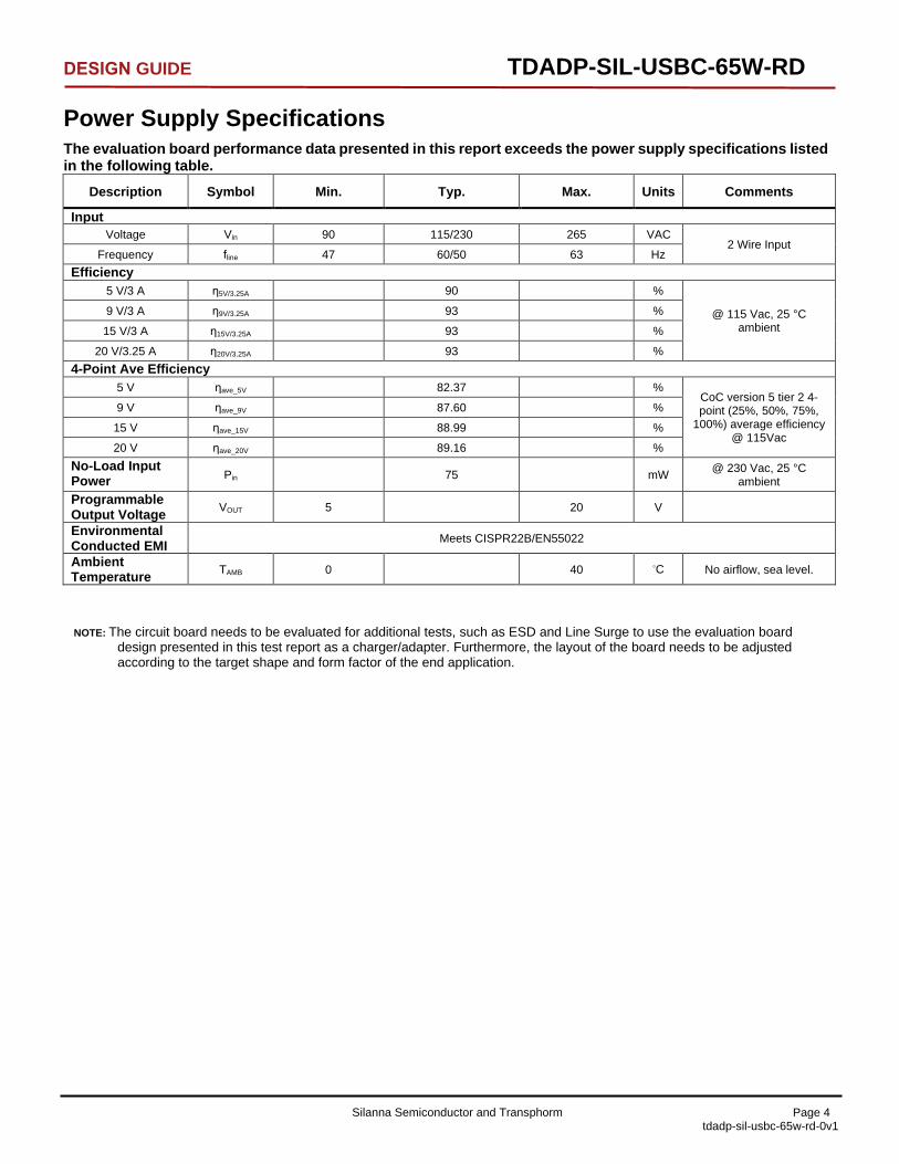
Power Supply Specifications The evaluation board performance data presented in this report exceeds the power supply specifications listed in the following table.
Description Symbol Min. Typ. Max. Units Comments
Input Voltage Vin 90 115/230 265 VAC
2 Wire Input Frequency fline 47 60/50 63 Hz
Efficiency 5 V/3 A η5V/3.25A 90 %
@ 115 Vac, 25 °C ambient
9 V/3 A η9V/3.25A 93 %
15 V/3 A η15V/3.25A 93 %
20 V/3.25 A η20V/3.25A 93 % 4-Point Ave Efficiency
5 V ηave_5V 82.37 % CoC version 5 tier 2 4- point (25%, 50%, 75%,
100%) average efficiency @ 115Vac
9 V ηave_9V 87.60 %
15 V ηave_15V 88.99 %
20 V ηave_20V 89.16 % No-Load Input Power Pin 75 mW @ 230 Vac, 25 °C
ambient Programmable Output Voltage VOUT 5 20 V
Environmental Conducted EMI Meets CISPR22B/EN55022
Ambient Temperature TAMB 0 40 °C No airflow, sea level.
NOTE: The circuit board needs to be evaluated for additional tests, such as ESD and Line Surge to use the evaluation board design presented in this test report as a charger/adapter. Furthermore, the layout of the board needs to be adjusted according to the target shape and form factor of the end application.
Silanna Semiconductor and Transphorm Page 5 tdadp-sil-usbc-65w-rd-0v1
TDADP-SIL-USBC-65W-RD
DESIGN GUIDE
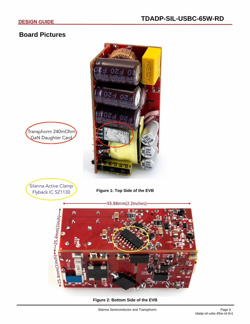
Board Pictures
Figure 1: Top Side of the EVB
Figure 2: Bottom Side of the EVB
Tushar Dhayagude
Tushar Dhayagude
Tushar Dhayagude
Tushar Dhayagude
Transphorm 240mOhmGaN Daughter Card
Tushar Dhayagude
Tushar Dhayagude
Silanna Active ClampFlyback IC SZ1130

Silanna Semiconductor and Transphorm Page 6 tdadp-sil-usbc-65w-rd-0v1
TDADP-SIL-USBC-65W-RD
DESIGN GUIDE
Schematic
Figure 3: 65W Schematic

Silanna Semiconductor and Transphorm Page 7 tdadp-sil-usbc-65w-rd-0v1
TDADP-SIL-USBC-65W-RD
DESIGN GUIDE
Circuit Description Input Protection The design incorporates a slow-acting input fuse (F1) as a form of protection in case of destructive failure of any of the downstream components. Furthermore, it has a varistor (RV1) connected between the line and neutral to absorb line surges and minimize the voltage overshoot seen by the downstream converter components. In addition, there is a footprint for an inrush current limiter (RT1) (negative temperature coefficient resistor) for applications which require attenuation of the inrush current.
EMI Filtering To meet the target EN55022 conducted EMI specification with sufficient margin with the least number of components and the highest power processing efficiency, the design utilizes an input filter consisting of an x-capacitor (C1) and a single common- mode choke (L1) as well as transformer (T1) construction for better EMI performance.
Fault Protections The evaluation board features Hiccup Mode Fault Protection using SZ1130-00. Under all applicable fault conditions, the device attempts to auto-restart. Table 1 below lists recovery behaviour under various fault conditions.
Table 1: SZ1130-00 Recovery Behavior
Fault Protection SZ1130
Input Under Voltage Lockout (UVLO)/ Brown-Out Auto-Recovery Input Over Voltage Lockout (OVLO) Auto-Recovery
Internal Over Temp Protection (OTP) Hiccup
External Over Temp Protection (OTP) Hiccup
Peak Current Limit (PCL) Hiccup
Over-Power Protection (OPP) Hiccup
Output Short Circuit (OSC) Hiccup
Silanna Semiconductor and Transphorm Page 8 tdadp-sil-usbc-65w-rd-0v1
TDADP-SIL-USBC-65W-RD
DESIGN GUIDE
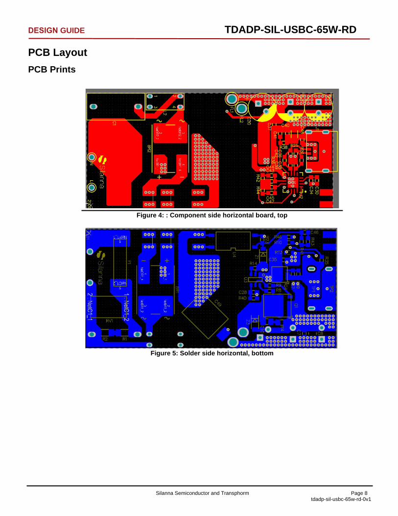
PCB Layout PCB Prints
Figure 4: : Component side horizontal board, top
Figure 5: Solder side horizontal, bottom
Silanna Semiconductor and Transphorm Page 9 tdadp-sil-usbc-65w-rd-0v1
TDADP-SIL-USBC-65W-RD
DESIGN GUIDE
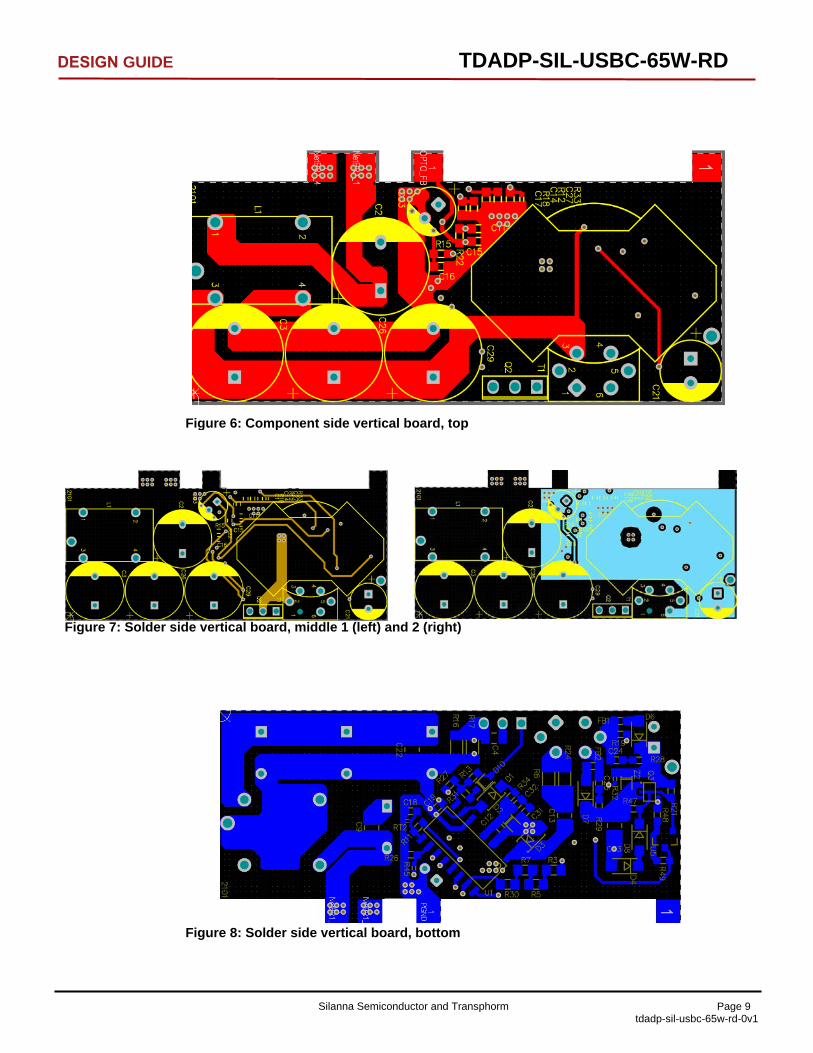
Figure 6: Component side vertical board, top
Figure 7: Solder side vertical board, middle 1 (left) and 2 (right)
Figure 8: Solder side vertical board, bottom
Silanna Semiconductor and Transphorm Page 10 tdadp-sil-usbc-65w-rd-0v1
TDADP-SIL-USBC-65W-RD
DESIGN GUIDE
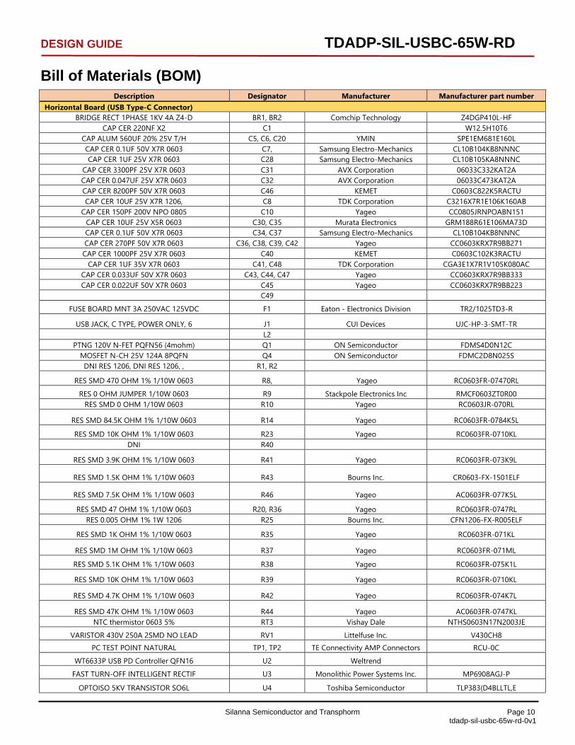
Bill of Materials (BOM) Description Designator Manufacturer Manufacturer part number
Horizontal Board (USB Type-C Connector)BRIDGE RECT 1PHASE 1KV 4A Z4-D BR1, BR2 Comchip Technology Z4DGP410L-HF
CAP CER 220NF X2 C1 W12.5H10T6 CAP ALUM 560UF 20% 25V T/H C5, C6, C20 YMIN SPE1EM681E160L CAP CER 0.1UF 50V X7R 0603 C7, Samsung Electro-Mechanics CL10B104KB8NNNC CAP CER 1UF 25V X7R 0603 C28 Samsung Electro-Mechanics CL10B105KA8NNNC
CAP CER 3300PF 25V X7R 0603 C31 AVX Corporation 06033C332KAT2A CAP CER 0.047UF 25V X7R 0603 C32 AVX Corporation 06033C473KAT2A CAP CER 8200PF 50V X7R 0603 C46 KEMET C0603C822K5RACTU CAP CER 10UF 25V X7R 1206, C8 TDK Corporation C3216X7R1E106K160AB
CAP CER 150PF 200V NPO 0805 C10 Yageo CC0805JRNPOABN151 CAP CER 10UF 25V X5R 0603 C30, C35 Murata Electronics GRM188R61E106MA73D CAP CER 0.1UF 50V X7R 0603 C34, C37 Samsung Electro-Mechanics CL10B104KB8NNNC CAP CER 270PF 50V X7R 0603 C36, C38, C39, C42 Yageo CC0603KRX7R9BB271 CAP CER 1000PF 25V X7R 0603 C40 KEMET C0603C102K3RACTU
CAP CER 1UF 35V X7R 0603 C41, C48 TDK Corporation CGA3E1X7R1V105K080AC CAP CER 0.033UF 50V X7R 0603 C43, C44, C47 Yageo CC0603KRX7R9BB333 CAP CER 0.022UF 50V X7R 0603 C45 Yageo CC0603KRX7R9BB223
C49
FUSE BOARD MNT 3A 250VAC 125VDC F1 Eaton - Electronics Division TR2/1025TD3-R
USB JACK, C TYPE, POWER ONLY, 6 J1 CUI Devices UJC-HP-3-SMT-TR L2
PTNG 120V N-FET PQFN56 (4mohm) Q1 ON Semiconductor FDMS4D0N12C MOSFET N-CH 25V 124A 8PQFN Q4 ON Semiconductor FDMC2D8N025S DNI RES 1206, DNI RES 1206, , R1, R2
RES SMD 470 OHM 1% 1/10W 0603 R8, Yageo RC0603FR-07470RL
RES 0 OHM JUMPER 1/10W 0603 R9 Stackpole Electronics Inc RMCF0603ZT0R00 RES SMD 0 OHM 1/10W 0603 R10 Yageo RC0603JR-070RL
RES SMD 84.5K OHM 1% 1/10W 0603 R14 Yageo RC0603FR-0784K5L
RES SMD 10K OHM 1% 1/10W 0603 R23 Yageo RC0603FR-0710KL DNI R40
RES SMD 3.9K OHM 1% 1/10W 0603 R41 Yageo RC0603FR-073K9L
RES SMD 1.5K OHM 1% 1/10W 0603 R43 Bourns Inc. CR0603-FX-1501ELF
RES SMD 7.5K OHM 1% 1/10W 0603 R46 Yageo AC0603FR-077K5L
RES SMD 47 OHM 1% 1/10W 0603 R20, R36 Yageo RC0603FR-0747RL RES 0.005 OHM 1% 1W 1206 R25 Bourns Inc. CFN1206-FX-R005ELF
RES SMD 1K OHM 1% 1/10W 0603 R35 Yageo RC0603FR-071KL
RES SMD 1M OHM 1% 1/10W 0603 R37 Yageo RC0603FR-071ML
RES SMD 5.1K OHM 1% 1/10W 0603 R38 Yageo RC0603FR-075K1L
RES SMD 10K OHM 1% 1/10W 0603 R39 Yageo RC0603FR-0710KL
RES SMD 4.7K OHM 1% 1/10W 0603 R42 Yageo RC0603FR-074K7L
RES SMD 47K OHM 1% 1/10W 0603 R44 Yageo AC0603FR-0747KL NTC thermistor 0603 5% RT3 Vishay Dale NTHS0603N17N2003JE
VARISTOR 430V 250A 2SMD NO LEAD RV1 Littelfuse Inc. V430CH8 PC TEST POINT NATURAL TP1, TP2 TE Connectivity AMP Connectors RCU-0C
WT6633P USB PD Controller QFN16 U2 Weltrend
FAST TURN-OFF INTELLIGENT RECTIF U3 Monolithic Power Systems Inc. MP6908AGJ-P
OPTOISO 5KV TRANSISTOR SO6L U4 Toshiba Semiconductor TLP383(D4BLLTL,E

Silanna Semiconductor and Transphorm
Page 11 tdadp-sil-usbc-65w-rd-0v1
TDADP-SIL-USBC-65W-RD
USER GUIDE
IC VREF SHUNT 36V 1% SOT23-3 U5 Texas Instruments ATL431AIDBZR
DIODE ZENER 24V 500MW SOD123, Z1 Diodes Incorporated DDZ24C-7,
DIODE ZENER 91V 500MW SOD123 Z3 ON Semiconductor MMSZ5270BT1G CAP CER 2.2nF 25V X7R 0603 C50 Murata Electronics
Vertical Board CAP ALUM 33UF 20% 400V T/H C2, C3, C26, C29 YMIN KCX(33UF-10X18P5) CAP CER 4.7UF 25V X6S 0603 C11 Murata Electronics GRM188C81E475KE11D
CAP CER 10000PF 25V X7R 0603 C12 KEMET C0603C103K3RACTU CAP CER 10000PF 25V X7R 0603 C14 Samsung Electro-Mechanics CL10B103KA8NNNC CAP CER 1000PF 16V X7R 0603 C15 Yageo CC0603KRX7R7BB102 CAP CER 10000PF 25V X7R 0603 C16 Samsung Electro-Mechanics CL10B103KA8NNNC
CAP CER 39PF 50V C0G/NP0 0603 C17 KEMET C0603C390J5GACTU CAP CER 10000PF 25V X7R 0603 C18 Samsung Electro-Mechanics CL10B103KA8NNNC
CAP CER 1UF 35V X7R 0603 C19 Taiyo Yuden GMK107AB7105KAHT CAP CER 100PF 200V NPO 0603 C24 Yageo CC0603JRNPOABN101 CAP CER 100PF 200V NPO 0603 C25 Yageo CC0603JRNPOABN101 CAP CER 150PF 16V X7R 0603 C27 Würth Elektronik 8.85012206029E+11
CAP CER 10000PF 630V X7R 1206, C9 KEMET C1206C103KBRACTU CAP CER 4700PF 630V X7R 1206, C13 TDK Corporation C3216X7R2J472K115AA CAP CER 10000PF 630V X7R 1206, C22 KEMET C1206C103KBRACTU
CAP CER 10UF 35V X7R 1206 C23 Samsung Electro-Mechanics CL31B106KLHNNNE CAP ALUM 68UF 80V 20% T/H C21 YMIN LKMC0902A190MF
CAP ALUM 47UF 20% 16V RADIAL C33 Rubycon 25YXJ47MTA5X11 DIODE GEN PURP 1KV 1A SOD123FA D1, D3 ON Semiconductor US1MFA
DIODE ZENER 4.7V 200MW D2 ON Semiconductor MM3Z4V7B DIODE ZENER 56V 200MW SOD323F Z2 ON Semiconductor MM3Z56VB
D4 D8
50NS 1A 300V HIGH EFFICIENT RECO
D6, D7 Taiwan Semiconductor
Corporation
HS1FFL DIODE SCHOTTKY 100V 250MA SOD323 D10 Nexperia USA Inc. BAT46WJ,115
FB1, FB2 CMC 9 mH 10X15 L1 CUSTOM_10X15
MOSFET 2N-CH 60V 0.35A Q3 Diodes Incorporated DMN61D9UDW-7 RES SMD 24.9 OHM 1% 3/4W 1206, R6 Vishay Dale CRCW120624R9FKEAHP
RES 0.18 OHM 1% 1/4W 1206 R16 Yageo, RL1206FR-070R18L RES 0.16 OHM 1% 1/2W 1206, R17 TE Connectivity Passive Product RLP73K2BR16FTDF
RES SMD 24.9 OHM 1% 3/4W 1206 R24 Vishay Dale CRCW120624R9FKEAHP RES SMD 22M OHM 1% 1/4W 0805, R3, R5, R7, R30 Stackpole Electronics Inc RMCF0805FT22M0
DNI RES 0805, R4 RES SMD 475K OHM 1% 1/10W 0603 R12 Yageo RC0603FR-07475KL
RES SMD 270 OHM 1/10W 0603 R13 Yageo RES SMD 10 OHM 1% 1/10W 0603 R15 Yageo RC0603FR-0710RL
RES SMD 14K OHM 0.1% 1/10W 0603 R18 Yageo RT0603BRD0714KL RES 120K OHM 1% 1/10W 0603 R19 Stackpole Electronics Inc RMCF0603FT120K RES 100K OHM 1% 1/10W 0603 R21 Stackpole Electronics Inc RMCF0603FT100K
RES SMD 10K OHM 1% 1/10W 0603 R22 Yageo RC0603FR-0710KL RES SMD 4.7 OHM 1% 1/10W 0603 R26 Yageo RC0603FR-074R7L
RES SMD 16.2K OHM 1% 1/10W 0603 R27 Yageo RC0603FR-0716K2L RES SMD 100 OHM 1% 1/10W 0603 R28 Yageo RC0603FR-07100RL RES SMD 47 OHM 1% 1/10W 0603 R29 Yageo RMCF0603FT47R0
RES SMD 3.3K OHM 1% 1/10W 0603 R34 Yageo RC0603FR-073K3L DNI R47
RES SMD 825K OHM 1% 1/10W 0603 R48 RES SMD 274K OHM 1% 1/10W 0603 R49 RES SMD 22K OHM 1% 1/10W 0603 R11 Yageo RC0603FR-0722KL
RES SMD 0 OHM 1/10W 0603 R31 Yageo RC0603JR-070RL RES SMD 619K OHM 1% 1/16W 0402, R32, Yageo RC0402FR-07619KL
Silanna Semiconductor and Transphorm Page 12 tdadp-sil-usbc-65w-rd-0v1
TDADP-SIL-USBC-65W-RD
DESIGN GUIDE
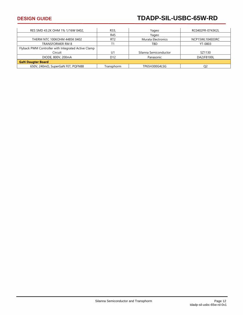
RES SMD 43.2K OHM 1% 1/16W 0402, R33, Yageo RC0402FR-0743K2L R45 Yageo
THERM NTC 100KOHM 4485K 0402 RT2 Murata Electronics NCP15WL104E03RC TRANSFORMER RM 8 T1 TBD YT-0803
Flyback PWM Controller with Integrated Active Clamp Circuit U1 Silanna Semiconductor SZ1130
DIODE, 800V, 200mA D12 Panasonic DA2JF8100L GaN Daugter Board
650V, 240mΩ, SuperGaN FET, PQFN88 Transphorm TP65H300G4LSG Q2

Silanna Semiconductor and Transphorm Page 13 tdadp-sil-usbc-65w-rd-0v1
TDADP-SIL-USBC-65W-RD
DESIGN GUIDE
Transformer Specification
Table 2: Transformer Material Lists

Silanna Semiconductor and Transphorm Page 14 tdadp-sil-usbc-65w-rd-0v1
TDADP-SIL-USBC-65W-RD
DESIGN GUIDE
Common-Mode Choke Specification
Table 3: Common-Mode Choke Material Lists
Material Specification Manufacturer Mfr. Part Number Core R12.5 × 7.90 × 6.35 mm dimension
(T38 -10000u) EPCOS/TDK or equivalent B64290L0742X038 or equivalent
AWG26 Magnet wire, dual insulation layer Various Separator PCB or Plastic
Silanna Semiconductor and Transphorm Page 15 tdadp-sil-usbc-65w-rd-0v1
TDADP-SIL-USBC-65W-RD
DESIGN GUIDE
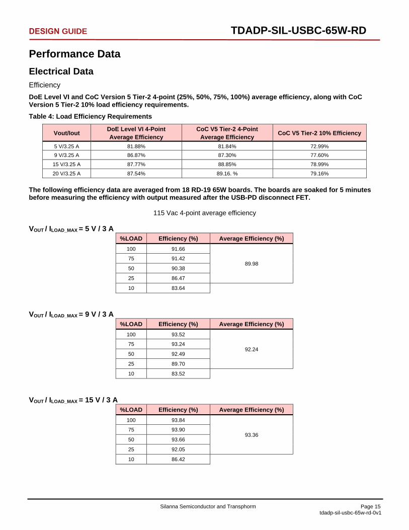
Performance Data Electrical Data Efficiency DoE Level VI and CoC Version 5 Tier-2 4-point (25%, 50%, 75%, 100%) average efficiency, along with CoC Version 5 Tier-2 10% load efficiency requirements. Table 4: Load Efficiency Requirements
Vout/Iout DoE Level VI 4-Point Average Efficiency
CoC V5 Tier-2 4-Point Average Efficiency CoC V5 Tier-2 10% Efficiency
5 V/3.25 A 81.88% 81.84% 72.99% 9 V/3.25 A 86.87% 87.30% 77.60%
15 V/3.25 A 87.77% 88.85% 78.99%
20 V/3.25 A 87.54% 89.16. % 79.16%
The following efficiency data are averaged from 18 RD-19 65W boards. The boards are soaked for 5 minutes before measuring the efficiency with output measured after the USB-PD disconnect FET.
115 Vac 4-point average efficiency
VOUT / ILOAD_MAX = 5 V / 3 A %LOAD Efficiency (%) Average Efficiency (%)
100 91.66
89.98 75 91.42
50 90.38
25 86.47
10 83.64
VOUT / ILOAD_MAX = 9 V / 3 A %LOAD Efficiency (%) Average Efficiency (%)
100 93.52
92.24 75 93.24
50 92.49
25 89.70
10 83.52
VOUT / ILOAD_MAX = 15 V / 3 A %LOAD Efficiency (%) Average Efficiency (%)
100 93.84
93.36 75 93.90
50 93.66
25 92.05
10 86.42
Silanna Semiconductor and Transphorm Page 16 tdadp-sil-usbc-65w-rd-0v1
TDADP-SIL-USBC-65W-RD
DESIGN GUIDE
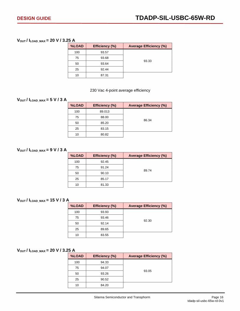
VOUT / ILOAD_MAX = 20 V / 3.25 A %LOAD Efficiency (%) Average Efficiency (%)
100 93.57
93.33 75 93.68
50 93.64
25 92.44
10 87.31
230 Vac 4-point average efficiency
VOUT / ILOAD_MAX = 5 V / 3 A %LOAD Efficiency (%) Average Efficiency (%)
100 89.013
86.34 75 88.00
50 85.20
25 83.15
10 80.82
VOUT / ILOAD_MAX = 9 V / 3 A %LOAD Efficiency (%) Average Efficiency (%)
100 92.45
89.74 75 91.24
50 90.10
25 85.17
10 81.33
VOUT / ILOAD_MAX = 15 V / 3 A %LOAD Efficiency (%) Average Efficiency (%)
100 93.93
92.30 75 93.46
50 92.14
25 89.65
10 83.55
VOUT / ILOAD_MAX = 20 V / 3.25 A %LOAD Efficiency (%) Average Efficiency (%)
100 94.33
93.05 75 94.07
50 93.26
25 90.52
10 84.20

Silanna Semiconductor and Transphorm Page 17 tdadp-sil-usbc-65w-rd-0v1
TDADP-SIL-USBC-65W-RD
DESIGN GUIDE
Full Load Efficiencies at 90Vac / 115Vac / 230Vac / 265Vac; 5V / 9V / 15V / 20V (measured after the USB-PD disconnect FET)
Vout = 5 V Vin Iout Efficiency (%)
90 Vac @ 50 Hz 3 A 91.46
115 Vac @ 60 Hz 3 A 91.66
230 Vac @ 50 Hz 3 A 89.01
265 Vac @ 50 Hz 3 A 88.27
Vout = 9 V Vin Iout Efficiency (%)
90 Vac @ 50 Hz 3 A 92.98
115 Vac @ 60 Hz 3 A 93.52
230 Vac @ 50 Hz 3 A 91.79
265 Vac @ 50 Hz 3 A 91.65
Vout = 15 V Vin Iout Efficiency (%)
90 Vac @ 50 Hz 3 A 93.10
115 Vac @ 60 Hz 3 A 93.84
230 Vac @ 50 Hz 3 A 93.94
265 Vac @ 50 Hz 3 A 93.52
Vout = 20 V Vin Iout Efficiency (%)
90 Vac @ 50 Hz 3.25 A 92.39
115 Vac @ 60 Hz 3.25 A 93.57
230 Vac @ 50 Hz 3.25 A 94.33
265 Vac @ 50 Hz 3.25 A 94.16
Silanna Semiconductor and Transphorm Page 18 tdadp-sil-usbc-65w-rd-0v1
TDADP-SIL-USBC-65W-RD
DESIGN GUIDE
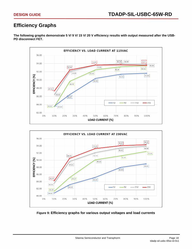
Efficiency Graphs
The following graphs demonstrate 5 V/ 9 V/ 15 V/ 20 V efficiency results with output measured after the USB- PD disconnect FET.
Figure 9: Efficiency graphs for various output voltages and load currents
Silanna Semiconductor and Transphorm Page 19 tdadp-sil-usbc-65w-rd-0v1
TDADP-SIL-USBC-65W-RD
DESIGN GUIDE
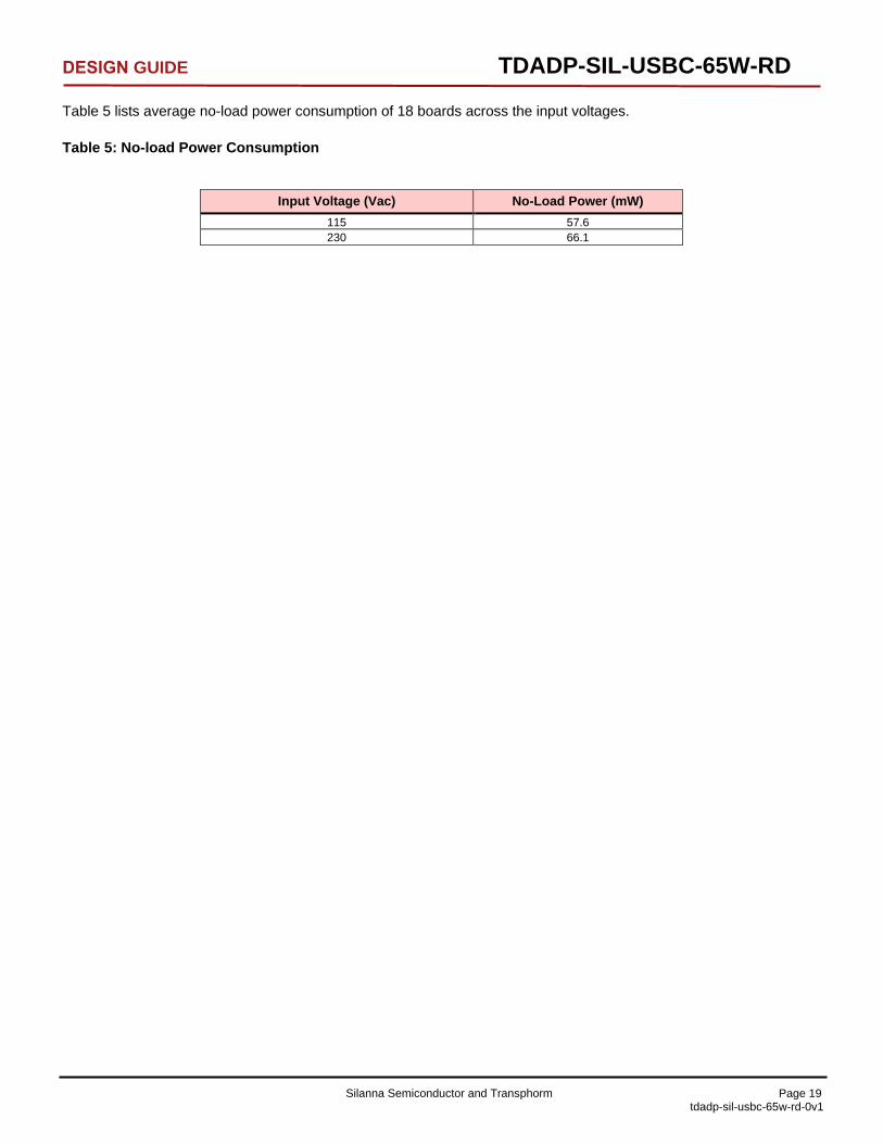
Table 5 lists average no-load power consumption of 18 boards across the input voltages.
Table 5: No-load Power Consumption
Input Voltage (Vac) No-Load Power (mW) 115 57.6 230 66.1
Silanna Semiconductor and Transphorm Page 20 tdadp-sil-usbc-65w-rd-0v1
TDADP-SIL-USBC-65W-RD
DESIGN GUIDE
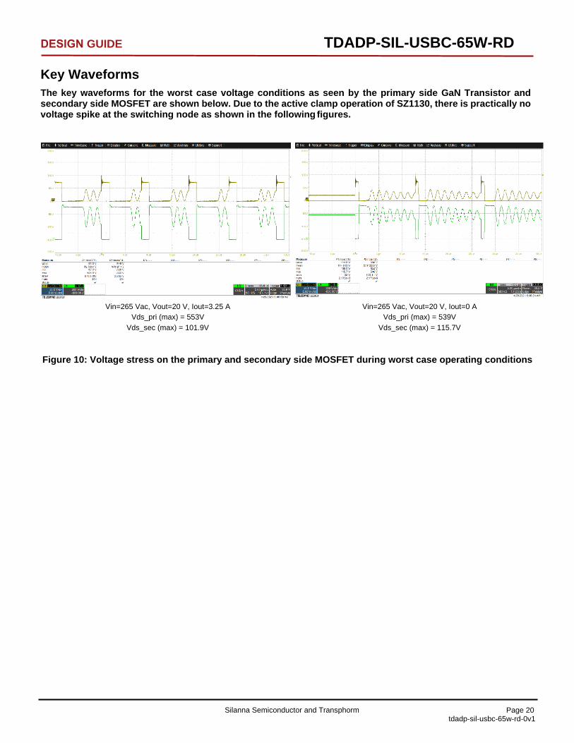
Key Waveforms The key waveforms for the worst case voltage conditions as seen by the primary side GaN Transistor and secondary side MOSFET are shown below. Due to the active clamp operation of SZ1130, there is practically no voltage spike at the switching node as shown in the following figures.
Vin=265 Vac, Vout=20 V, Iout=3.25 A Vds_pri (max) = 553V
Vds_sec (max) = 101.9V
Vin=265 Vac, Vout=20 V, Iout=0 A Vds_pri (max) = 539V
Vds_sec (max) = 115.7V
Figure 10: Voltage stress on the primary and secondary side MOSFET during worst case operating conditions
Silanna Semiconductor and Transphorm Page 21 tdadp-sil-usbc-65w-rd-0v1
TDADP-SIL-USBC-65W-RD
DESIGN GUIDE
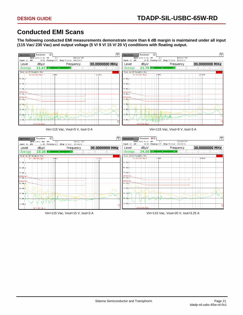
Conducted EMI Scans The following conducted EMI measurements demonstrate more than 6 dB margin is maintained under all input (115 Vac/ 230 Vac) and output voltage (5 V/ 9 V/ 15 V/ 20 V) conditions with floating output.
Vin=115 Vac, Vout=5 V, Iout=3 A Vin=115 Vac, Vout=9 V, Iout=3 A
Vin=115 Vac, Vout=15 V, Iout=3 A Vin=115 Vac, Vout=20 V, Iout=3.25 A

Silanna Semiconductor and Transphorm Page 22 tdadp-sil-usbc-65w-rd-0v1
TDADP-SIL-USBC-65W-RD DESIGN GUIDE
Vin=230 Vac, Vout=5 V, Iout=3 A Vin=230 Vac, Vout=9 V, Iout=3 A
Vin=230 Vac, Vout=15 V, Iout=3 A Vin=230 Vac, Vout=20 V, Iout=3.25 A
Figure 11: Conducted EMI test results under various operating conditions

Silanna Semiconductor and Transphorm Page 23 tdadp-sil-usbc-65w-rd-0v1
TDADP-SIL-USBC-65W-RD DESIGN GUIDE
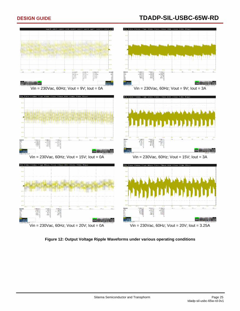
Output Voltage Ripple Noise The output voltage ripple was measured using a voltage probe with two capacitors (1 µF/50 V ceramic and 33 µF/50 V
low ESR electrolytic) tied in parallel across it. Measurement done at load side using an E-Mark USB cable.
Table 6: Output Voltage Ripple Summary
Input Voltage (Vac) Vout / Iout Measured Output Ripple (mVpk-pk)
115
5V / 0A 34.67 5V / 3A 40.53 9V / 0A 22.18 9V / 3A 46.71
15V / 0A 19.64 15V / 3A 52.67 20V / 0A 21.24
20V / 3.25A 77.64
230
5V / 0A 67.02 5V / 3A 45.56 9V / 0A 40.27 9V / 3A 36.09
15V / 0A 34.49 15V / 3A 46.93 20V / 0A 29.91
20V / 3.25A 55.56
a. 115Vac 60Hz
Vin = 115Vac, 60Hz; Vout = 5V; Iout = 0A Vin = 115Vac, 60Hz; Vout = 5V; Iout = 3A
Vin = 115Vac, 60Hz; Vout = 9V; Iout = 0A Vin = 115Vac, 60Hz; Vout = 9V; Iout = 3A
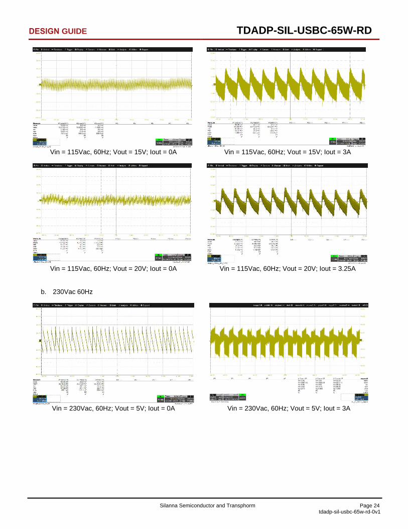
Silanna Semiconductor and Transphorm Page 24 tdadp-sil-usbc-65w-rd-0v1
TDADP-SIL-USBC-65W-RD DESIGN GUIDE
Vin = 115Vac, 60Hz; Vout = 15V; Iout = 0A Vin = 115Vac, 60Hz; Vout = 15V; Iout = 3A
Vin = 115Vac, 60Hz; Vout = 20V; Iout = 0A Vin = 115Vac, 60Hz; Vout = 20V; Iout = 3.25A
b. 230Vac 60Hz
Vin = 230Vac, 60Hz; Vout = 5V; Iout = 0A Vin = 230Vac, 60Hz; Vout = 5V; Iout = 3A
Silanna Semiconductor and Transphorm Page 25 tdadp-sil-usbc-65w-rd-0v1
TDADP-SIL-USBC-65W-RD DESIGN GUIDE
Vin = 230Vac, 60Hz; Vout = 9V; Iout = 0A Vin = 230Vac, 60Hz; Vout = 9V; Iout = 3A
Vin = 230Vac, 60Hz; Vout = 15V; Iout = 0A Vin = 230Vac, 60Hz; Vout = 15V; Iout = 3A
Vin = 230Vac, 60Hz; Vout = 20V; Iout = 0A Vin = 230Vac, 60Hz; Vout = 20V; Iout = 3.25A
Figure 12: Output Voltage Ripple Waveforms under various operating conditions

Silanna Semiconductor and Transphorm Page 26 tdadp-sil-usbc-65w-rd-0v1
TDADP-SIL-USBC-65W-RD DESIGN GUIDE
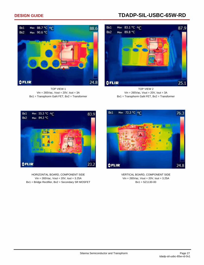
Thermal Measurements The key component temperatures are shown below for 90Vac and 265Vac full load (20V/65W) operating conditions after 1hr bake time.
RefDes Description Temp. at 90Vac Temp. at 265Vac U1 SZ1130-00 83.1 72.3
BR1 Bridge Rectifier 92.2 55.3
T1 Transformer 93.1 90.6
Q2 Transphorm GaN Device 91.4 88.7
Q1 Secondary SR MOSFET 87.7 84.3
TOP VIEW 1 Vin = 90Vac, Vout = 20V, Iout = 3.25A
Bx1 = Transphorm GaN FET, Bx2 = Transformer
TOP VIEW 2 Vin = 90Vac, Vout = 20V, Iout = 3.25
Bx1 = Transphorm GaN FET, Bx2 = Transformer
HORIZONTAL BOARD, COMPONENT SIDE Vin = 90Vac, Vout = 20V, Iout = 3.25A
Bx1 = Bridge Rectifier, Bx2 = Secondary SR MOSFET
VERTICAL BOARD, COMPONENT SIDE Vin = 90Vac, Vout = 20V, Iout = 3.25A
Bx1 = SZ1130-00
Silanna Semiconductor and Transphorm Page 27 tdadp-sil-usbc-65w-rd-0v1
TDADP-SIL-USBC-65W-RD DESIGN GUIDE
TOP VIEW 1 Vin = 265Vac, Vout = 20V, Iout = 3A
Bx1 = Transphorm GaN FET, Bx2 = Transformer
TOP VIEW 2 Vin = 265Vac, Vout = 20V, Iout = 3A
Bx1 = Transphorm GaN FET, Bx2 = Transformer
HORIZONTAL BOARD, COMPONENT SIDE Vin = 265Vac, Vout = 20V, Iout = 3.25A
Bx1 = Bridge Rectifier, Bx2 = Secondary SR MOSFET
VERTICAL BOARD, COMPONENT SIDE Vin = 265Vac, Vout = 20V, Iout = 3.25A
Bx1 = SZ1130-00

Document 11075 Ver. 1.0
Revision History Revision Date Author Note
1.0 Mar. 12, 2021 Results collected and report generated.
2.0 Apr. 28, 2021 Average data for 18 boards.
Hardware Info Info Value
Timestamp April 29, 2021 Primary IC Silanna Semiconductor Integrated Flyback PWM Controller (SZ1130-00)
Primary Switch Transphorm 650 V SuperGaN™ FET (TP65H300G4LSG) Secondary IC Weltrend WT6633P
AC Supply Chroma Programable AC Source, 61502 Input Meter Yokogawa WT310E
Output Meter Chroma 66205 Oscilloscope Teledyne Lecroy HD04054A
No-load bake time 300 Input voltages [(90, 60), (115, 60), (230, 50), (265, 50)]
Output voltages [5, 9, 15, 20]
Silanna Semiconductor Proprietary and Confidential Information furnished by Silanna Semiconductor is believed to be accurate and reliable. However, no responsibility is assumed for its use. Silanna Semiconductor makes no representation that the interconnection of its circuits as described herein will not infringe on existing patents rights.
4795 Eastgate Mall, Suite 100, San Diego, CA 92121 Toll Free: (888) 637-3564 | Fax: (858) 373-0437 | www.PowerDensity.com
Page 28