
Design, Fabrication and Characterization of Plasmonic ...
108
University of Arkansas, Fayeeville ScholarWorks@UARK eses and Dissertations 12-2013 Design, Fabrication and Characterization of Plasmonic Fishnet Structures for the Enhancement of Absorption in in Film Solar Cells Sayan Seal University of Arkansas, Fayeeville Follow this and additional works at: hp://scholarworks.uark.edu/etd Part of the Electronic Devices and Semiconductor Manufacturing Commons , and the Power and Energy Commons is esis is brought to you for free and open access by ScholarWorks@UARK. It has been accepted for inclusion in eses and Dissertations by an authorized administrator of ScholarWorks@UARK. For more information, please contact [email protected], [email protected]. Recommended Citation Seal, Sayan, "Design, Fabrication and Characterization of Plasmonic Fishnet Structures for the Enhancement of Absorption in in Film Solar Cells" (2013). eses and Dissertations. 969. hp://scholarworks.uark.edu/etd/969
Transcript of Design, Fabrication and Characterization of Plasmonic ...

University of Arkansas, FayettevilleScholarWorks@UARK
Theses and Dissertations
12-2013
Design, Fabrication and Characterization ofPlasmonic Fishnet Structures for the Enhancementof Absorption in Thin Film Solar CellsSayan SealUniversity of Arkansas, Fayetteville
Follow this and additional works at: http://scholarworks.uark.edu/etd
Part of the Electronic Devices and Semiconductor Manufacturing Commons, and the Power andEnergy Commons
This Thesis is brought to you for free and open access by ScholarWorks@UARK. It has been accepted for inclusion in Theses and Dissertations by anauthorized administrator of ScholarWorks@UARK. For more information, please contact [email protected], [email protected].
Recommended CitationSeal, Sayan, "Design, Fabrication and Characterization of Plasmonic Fishnet Structures for the Enhancement of Absorption in ThinFilm Solar Cells" (2013). Theses and Dissertations. 969.http://scholarworks.uark.edu/etd/969

Design, Fabrication and Characterization of Plasmonic Fishnet Structures for the Enhancement
of Absorption in Thin Film Solar Cells

Design, Fabrication and Characterization of Plasmonic Fishnet Structures for the Enhancement
of Absorption in Thin Film Solar Cells
A thesis submitted in partial fulfillment
of the requirements for the degree of
Master of Science in Electrical Engineering
By
Sayan Seal
University of Calcutta
Bachelor of Science in Physics, 2008
University of Calcutta Post Bachelor of Science Bachelor of Technology in Radio Physics and Electronics, 2011
December 2013
University of Arkansas
This thesis is approved for recommendation to the Graduate Council.
____________________________________
Dr. Vasundara V. Varadan
Thesis Director
____________________________________ _____________________________________
Dr. Hameed Naseem Dr. Shui-Qing Yu
Committee Member Committee Member

Abstract
Incorporating plasmonic structures into the back spacer layer of thin film solar cells
(TFSCs) is an efficient way to improve their performance. The fishnet structure; which is a
tunable, plasmonic light scatterer is used to enhance light absorption. Unlike other plasmonic
particles that have been previously suggested, the fishnet is an electrically connected wire mesh
and does not result in electric field localization, hence it results in greater absorption in the
intrinsic Si layer. Unlike other designs, the fishnet structure is placed in the back spacer layer of
the TFSC, so it does not block any incident light. There is also the possibility of integrating back
contacts with the fishnet for efficient carrier collection. In addition to its performance, the fishnet
structure can be fabricated using low cost nano-imprinting techniques.
The fishnet structure has been studied theoretically in previous research, but this is the
first time that the performance of the fishnet has been verified experimentally. The fishnet
structure originally proposed in the theoretical study was made of gold, but keeping industrial
viability in mind, the choice of metal was changed to silver for this study. The design for the
silver fishnet was optimized using full wave electromagnetic simulations in the High Frequency
Structure Simulator (HFSS) by Ansoft. The design geometry was tailored to resonate at the band
gap of the absorber material (Si), where the absorption coefficient of Si is very low. The goal
was to enhance absorption in this region, without causing any degradation of absorption in the
other parts of the spectrum.
The silver fishnet structure was fabricated using Electron Beam Lithography (EBL) and
thermal evaporation. The other layers of the thin film solar cell (TFSC) were deposited on top of
this structure, so that the final fabricated structure optically resembled a TFSC. The absorption of

the sample was measured using Spectroscopic Ellipsometry (SE) and was compared with the
absorption of a control sample sans the fishnet. It was shown that light absorption is enhanced by
a factor of 12.8at the resonance frequency due to the presence of the fishnet structure. The short
circuit current (JSC) increased by 30%. Not only was there no observed degradation at other
wavelengths, but the overall absorption also increased as a result of using the fishnet.
Even though the fishnet served its purpose of absorption enhancement, there was little
correlation between the results of numerical simulations and experimental results. Numerical
simulations use values of optical properties from literature as input. These values differ
considerably from the materials actually used to fabricate an experimental sample. Also the layer
above the fishnet is assumed to be perfectly flat in the numerical model, which is not the case.
The 20 nm thickness of the fishnet causes bumps at the AZO –Si interface that must be
accounted for given the small thickness of the TFSC layers. The materials used to fabricate the
fishnet TFSC were characterized individually using SE. The existence of a bump atop the fishnet
was verified using Atomic Force Microscopy (AFM). These factors were included in the
theoretical model and the structure was re-simulated to give a much better agreement between
theory and experiment.
A fishnet structure in the back spacer layer of a TFSC is proposed to enhance
performance efficiency of the TFSC. Nanoimprinting techniques and roll to roll manufacturing
can be used to economically fabricate such TFSCs on an industrial scale.

Acknowledgements
I would like to sincerely thank Dr. Vasundara V. Varadan for her invaluable mentorship
and support through my MS degree.
I would like to thank Prof. Hameed Naseem and Prof. Shui-Qing Yu for agreeing to serve
as part of my committee, and for the guidance and support they have offered throughout.
I would like to thank Prof. J. Cui and Prof. A. Bhattacharyya of the University of
Arkansas, Little Rock, for their help and support in our collaborative efforts.
I would like to thank Dr. Mourad Benamara (University of Arkansas) for training me in
Scanning Electron Microscopy and Dr. Michael Hawkridge (University of Arkansas) for training
me in Atomic Force Microscopy. I would like to thank Mr. Errol Porter (University of
Arkansas), for his support during using the equipment at the High density Electronics Center
(HiDEC), University of Arkansas.
I would like to appreciate all the help from my colleagues, especially Dr. InKwang Kim,
Dr. Liming Ji, and Dr. Vinay Budhraja.
The work in this dissertation is supported by the National Science Foundation under
EPS–1003970.

Table of Contents
Chapter 1: Introduction .......................................................................................................... 1
Chapter 2: Background and Motivation ................................................................................. 6
2.1 Motivation for Thin Film Solar Cells ............................................................................... 6
2.2 Light Trapping in Thin Film Solar Cells ........................................................................ 10
Chapter 3: Experimental Details .......................................................................................... 22
3.1 Design of the Fishnet Structure for a Thin Film Solar Cell ........................................... 23
3.2 Fabrication of the Thin Film Solar Cell with Fishnet .................................................... 24
3.3 Measurement of Total Absorption of the Thin Film Solar Cell With and Without the
Fishnet Structure ....................................................................................................................... 40
3.3(A): Material Characterization ....................................................................................... 46
3.3(B): Reflection Measurements Using an Ellipsometer ................................................... 47
3.4 Modification of the Numerical Model and Comparison with Experimental Results .......... 51
Chapter 4: Results and Discussions ..................................................................................... 53
4.1. Design of the Thin Film Solar cell with a Fishnet Structure in the Back Spacer Layer .... 53
4.2 Fabrication of the Fishnet Pattern using Electron Beam Lithography ................................ 57
4.3 Measurement of Total Absorption of the Fabricated Samples ....................................... 65
4.4 Ellipsometric Characterization and Structural Modification of Numerical Model ........... 71

4.4.1 Effects of using Ellipsometry-determined Optical Constants in the Numerical Model
............................................................................................................................................... 72
4.4.2 Structural Modifications in the Numerical Model...................................................... 77
Chapter 5: Conclusions and Future Work ............................................................................ 82
References………………………………………………………………………………………..84
Appendix 1: License for Figure 2.1 .............................................................................................. 90

List of Figures
Figure 2.1: Price of crystalline silicon photovoltaic cells in $/ watt
…...……………………………………………………………………………………6
Figure 2.2: Cost breakdowns in wafer solar cell processing……………………………………...7
Figure 2.3: Schematic of a typical thin film solar cell…………………………………………….9
Figure 2.4: Illustration of light trapping using rough surfaces…………………………………..12
Figure 2.5: Escape cone defined by the critical angle…………………………………………...12
Figure 2.6: Nanodome structure for solar cells…………………………………………………..14
Figure 2.7: Electric field enhancement around a gold nanoparticle embedded within SiO2…….16
Figure 2.8: Fishnet Structure for thin film solar cells……………………………………………17
Figure 2.9: Absorption co-efficient as a function of wavelength for amorphous silicon………..18
Figure 3.1: Model of the fishnet TFSC constructed in HFSS……………………………………23
Figure 3.2: Schematic showing the fabrication process for the fishnet thin film solar cell……...24
Figure 3.3: The JEOL JBX 5500ZD, High Density Electronics Center (HiDEC), University of
Arkansas…………………………………………………………………………….26
Figure 3.4: Schematic of spin coating……………………………………………………………27
Figure 3.5: Schematic of metal deposition after development…………………………………..28
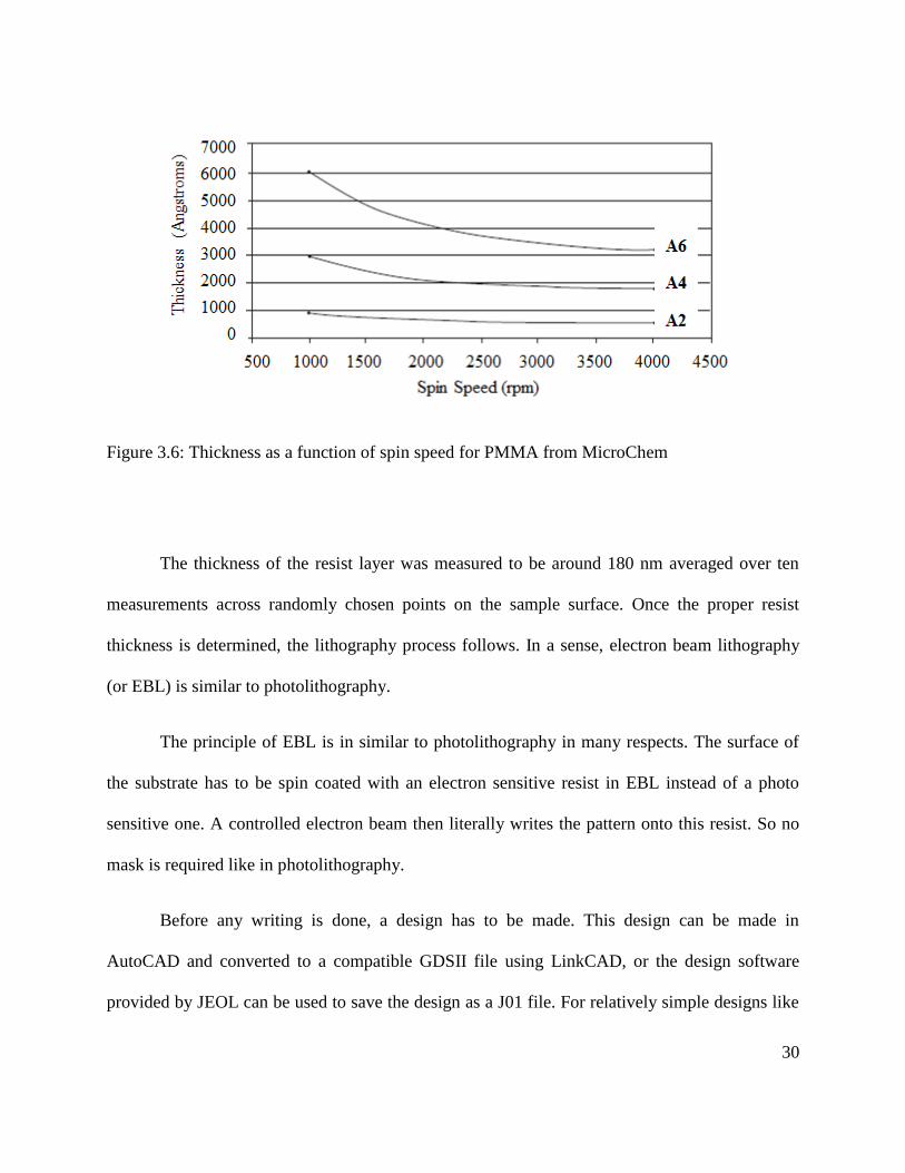
Figure 3.6: Thickness as a function of spin speed for PMMA from MicroChem……………….30
Figure 3.7: File conversion in the JEOL JBX 5500ZD………………………………………….31
Figure 3.8: Schematic showing the concept of a field…………………………………………...32
Figure 3.9: Schematic of the JEOL JBX 5500…………………………………………………...33
Figure 3.10: Laser beam controlled sample stage of the JEOL JBX 5500ZD…………………...36
Figure 3.11: Deflection correction in the JEOL JBX 5500ZD…………………………………..37
Figure 3.12 (a) V-VASE system at the University of Arkansas, Fayetteville. (b) Heat stage (c)
Rotating stage (d) Focus probes mounted on the source and detector units........41
Figure 3.13: Beam spot positioned within the fishnet pattern area………………………………42
Figure 3.14 (a) Screenshot of the X-Y alignment process in the WVASE software (b) Screenshot
of the Z-alignment process in the WVASE software……………………………44

Figure 3.15: Graph showing accurate fits between measured and fitted calibration data……….45
Figure 3.16: Baseline measurement for ambient light…………………………………………...47
Figure 3.17: Fit for Ψ and Δ for the standard sample……………………………………………48
Figure 3.18: Transmission through the fishnet TFSC…………………………………………...50
Figure 4.1: (a) Total absorption of the TFSC with and without the Fishnet (b) Layer-wise
absorption in the TFSC with the Fishnet………………………………………...54
Figure 4.2: Electric field in the a-Si layer of the fishnet TFSC computed using HFSS…………56
Figure 4.3: SEM pictures for a dose of 1500 μC/cm2 and a design linewidth of 100 nm (a) Pattern
uniform over large area (b) Linewidth of 200 nm obtained on an average…………58
Figure 4.4: Using a smaller dose results in underdeveloped pattern…………………………….59
Figure 4.5: Optimization of development time…………………………………………………..60
Figure 4.6: Design linewidth reduced to 85nm, development time reduced to 30 seconds……..61
Figure 4.7: Final dose optimization step…………………………………………………………63
Figure 4.8: 100 nm linewidth pattern using a dose of 800 μC/ cm2, design linewidth of 85 nm,
and develop time of 25 seconds…………………………………………………….64
Figure 4.9: Comparison of total absorption with and without fishnet…………………………...66
Figure 4.10: Consistent results for measurements taken for four different samples…………….68
Figure 4.11: Measurements consistent for different polarization states…………………………69
Figure 4.12: Comparison between numerical simulation and experimental results (a) With fishnet
(b) Without fishnet…………………………………………………………………70
Figure 4.13: Characterization of the Silicon……………………………………………………..73
Figure 4.14: Characterization of the 100 nm film of silver on silicon substrate………………...73
Figure 4.15: Characterization of the 100 nm chromium film on silicon substrate………………74
Figure 4.16: Characterization of the 20 nm AZO on silicon substrate…………………………..74
Figure 4.17: Characterization of the 500 nm a-Si on silicon substrate…………………………..75
Figure 4.18: Effect of numerical simulation using optical constants determined from ellipsometry
(a) Without fishnet (b) With fishnet………………………………………………..76
Figure 4.19: Structural modification used in the numerical model (a) Schematic of bump over
fishnet (b) Result of AFM measurements taken over the fishnet structure………..79
Figure 4.20: Result of including the bump on top of the fishnet in the numerical model……….80

List of Tables
Table 3.1: Recipe for spin coating……………………………………………………………….29
Table 3.2: Operating modes of the JEOL JBX 5500ZD…………………………………………34
Table 4.3: JSC comparison with and without the fishnet structure……………………………….67

1
Chapter 1: Introduction
This thesis deals with the enhancement of efficiency of thin film solar cells. A number of
parameters within a thin film solar cell that can lead directly to an increase in efficiency are
currently under study. Choice of semiconductor material for the absorber layer (amorphous
silicon, cadmium telluride, copper indium gallium diselenide, etc.), high quality contacts, anti-
reflection coatings—all of these factors are known to impact the efficiency in a positive way.
Incorporating plasmonic structures within the back spacer of thin film solar cells (TFSCs) is yet
another efficient way to improve the cell parameters. In this thesis a plasmonic fishnet structure
embedded in the back spacer layer of a TFSC is studied. The incorporation of this structure
results in an enhancement of light absorption in a-Si, which is used as the absorber material in
the thin film solar cell under test.
Thin film silicon solar cells are a better alternative to crystalline silicon solar cells due to
numerous advantages like reduced cost, low temperature processing, higher open-circuit voltage
and the fact that it can be easily deposited on various substrates without any issues with
uniformity. Because of the low minority carrier diffusion length and high recombination rate in
the p and n layers of TFSCs, the only way to improve the efficiency is to increase the absorption
in the amorphous silicon layer. In wafer solar cells, the thickness of silicon is around 180
microns, hence an incoming photon traverses a sufficient path length to get absorbed. In
addition, most wafer solar cells use a metallic back reflector that doubles as a back electrode.
This doubles the path length of the photon and constitutes one of the simplest light trapping
schemes. In thin film solar cells, an enhancement in path length cannot be achieved using such a
simple scheme; doubling the path length is far from enough. Rather, a scheme that could scatter

2
the light within the absorber layer and keep it confined horizontally (waveguide modes) would
increase the path length sufficiently, and increase the chance of the photon being absorbed.
There are various techniques used in the processing of TFSCs to enhance the absorption:
surface texturing, use of transparent conducting oxide, deposition of amorphous nano-crystalline
silicon, etc. Incident light is scattered by the textured surface, and upon reaching the interfaces,
the angle of incidence exceeds the critical angle, reflecting the light back into the absorber. This
procedure is repeated several times, trapping the light within the absorber layer.
Although these methods are highly cost effective, they do not perform satisfactorily as
light trapping designs. Using random surface texturing results in limited absorption enhancement
and plateau at an upper limit. Also the surface recombination increases due to rough surfaces.
The incorporation of plasmonic nanostructures within the spacer layers also enhances the
absorption in TFSCs. The effect of these structures on the performance of TFSC’s has been
studied experimentally as well as theoretically. But including plasmonic structures made of noble
metals has a huge impact on the cost of manufacturing these cells. Therefore unless the
advantage of this process is really significant as compared to cheaper alternatives like surface
texturing, and economical fabrication methods such as nanoimprinting can be developed, it may
not mature into a viable industrial practice.
Metal nanoparticles enclosed within a dielectric absorb incident photons at specific
wavelengths depending upon their size. The absorbed photons are radiated diffusely, and the
scattering pattern depends on the geometry of the plasmonic structure. This also gives us the
same scattering effect as surface texturing, but with several advantages. The size of nanoparticles
is much smaller, and more importantly, the scattering can be tailored to occur at a specific
3
frequency. The material, geometry, and layout of these particles define the frequency at which
they will absorb photons, and subsequently radiate.
Many research groups have reported an increase in absorption in plasmonic solar cells
using metallic nanoparticles arrays in the front spacer layer. Although there is significant
enhancement, a lot of light is also lost due to shadowing. It has also been demonstrated that using
plasmonic structures at the back spacer is a better alternative, especially when the enhancement
has to be targeted at longer wavelengths which uses larger nanoparticles (Ji and Varadan).
Despite the reported enhancement achieved by nanoparticles, one fact still remains—due
to the high electric field localization around the nanoparticles, the loss is very high. The reason
for this localization is that the nanoparticles are electrically isolated. A scheme whereby these
particles could be electrically interconnected could solve this issue.
The plasmonic fishnet structure is one such geometry by which this effect can be
realized. As its name suggests, it is a two dimensional net made of a thin film of metal. The
ability of this structure to enhance the absorption and short-circuit current density in thin film
solar cells has already been established theoretically through numerical simulations (Ji and
Varadan). In accordance with this design a plasmonic fishnet was embedded within the back
spacer layer of a thin film solar cell structure. The incoming light is scattered into the absorber
layer and trapped by total internal reflection from the top interface of the absorber layer. This
increases the effective path length of the photon within the absorber material and increases the
probability of the photon being absorbed and converted into an electron-hole pair. So despite
being a very thin film, the absorber seems to be much thicker in effect.

4
The fishnet is inherently different from a regular scatterer; the frequency of operation can
be tuned in the fishnet. The linewidth, pitch size, thickness and choice of material define the
plasmonic resonant frequency of this structure. For this specific case, the fishnet was designed to
provide a plasmonic resonance at the bandgap of a-Si, which corresponds to a wavelength of
around 680 nm. The absorption of a-Si is very weak in this region. Silver was used to make the
fishnet structure, and the design was optimized using full wave electromagnetic simulations in
the High Frequency Structure Simulator (HFSS) by Ansoft.
The fishnet structure made of silver was fabricated using electron beam lithography and
thermal evaporation. The final fabricated structure optically resembled a TFSC. The results
predicted by numerical simulations were reproduced experimentally on a fabricated sample. The
reflection from the sample was measured using spectroscopic ellipsometry, and the absorption in
the absorber layer was computed from these measurements. The results were compared with a
thin film solar cell without the fishnet and it was found that the absorption was enhanced by a
factor of 12.8 at the resonance frequency. In fact, there was an increase in the overall absorption
across the entire wavelength range as well. With plasmonic structures made of noble metals, it is
always a matter of concern whether the trapped energy is being successfully absorbed. It could
also be expended as loss in the metal. It was shown that in this case, 83% of the absorbed power
was absorbed successfully by the absorber layer. The structure intensifies the electric field within
the absorber layer, with marginal loss in the metal.
When the results of the experiment were compared with the results predicted by
numerical simulations, it was found that the agreement was poor. This was a matter of concern
because it introduced a large degree of uncertainty while predicting how these structures

5
behaved. Upon further investigation, it was found that the material properties as well the surface
morphology of the thin film solar cell under test were described inaccurately by the existing
model. After appropriate modifications were made, the agreement between theory and
experiment showed good agreement.
In this thesis, a complete account of fabricating a plasmonic design for a thin film solar
cell has been discussed. An existing design was modified to offer a low cost alternative. A full
fabrication process for the design has been developed and reiterated several times to check for
repeatability. Although the EBL process is very slow for processing these cells on a commercial
scale, nanoimprinting facilities can be used to produce them as part of an assembly line. When
all these cells were tested optically for absorption, it was found that the absorption was enhanced
as a result of including the fishnet. As a conclusion to this study, the experimental results were
used to improve the numerical model, which will aid in the engineering of similar structures in
the future.

6
Chapter 2: Background and Motivation
2.1 Motivation for Thin Film Solar Cells
The cost per watt of solar cell technology has been on the decline since its inception.
Figure 2.1 shows that the cost per watt of a crystalline silicon solar cell module today is less than
one hundredth of its cost in 1977 [1]. The question, however, is that is this enough to make solar
energy a viable option in the future? The short answer is no. Despite falling prices, solar energy
is still far more expensive than other options available in renewable energy: like wind, hydro-
electricity, biomass, and geothermal [2]. Unless steps are taken to bring this cost down, there is
little chance that solar cells will see the light of day as a viable source of clean energy.
Figure 2.1: Price of crystalline silicon photovoltaic cells in $/ watt [1]

7
Figure 2.2 gives the cost breakdown in the manufacture of a wafer solar cell [3, 4]. It can
be seen that the 67% of the cost is that of the wafer itself, with 22% of the cost incurred by the
metallization process. Hence if the cost in the two aforementioned areas can be reduced
significantly, the overall cost of production will also decrease significantly. This is the point at
which Thin Film Solar Cells (TFSCs) assume importance.
Figure 2.2 Cost breakdowns in wafer solar cell processing
Thin film solar cells are the way forward for the solar cell industry. Thin film solar cells
use 90% less material as compared to conventional wafer solar cells. This drastically reduces the
cost of manufacturing thin film solar cell modules. They have numerous other advantages—low

8
cost processing, easy deposition methods and less raw material requirement. A detailed
discussion on the impact of thin film silicon solar cells was given by A. Shah et al, 1999 [5]. The
possibility of cutting costs by employing roll-to-roll manufacture methods was also discussed.
Fig. 2.2 shows a simple schematic of a typical TFSC. The substrate used is typically
glass, with a back electrode made of a thin film of metal (silver, gold, aluminum, copper, etc.).
Above this layer there is a back spacer layer made of a transparent conductive oxide like Indium
Tin Oxide (ITO) or Aluminum-doped Zinc Oxide (AZO). Following this, we have the
semiconductor layer that actually absorbs photons and generates an electron-hole pair. The
choice of material for this layer ranges from amorphous Silicon (a-Si), to Cadmium Telluride
(CdTe), to the more recently developed Copper Indium Gallium Diselenide (CIGS) and CZTS
cells. Amorphous silicon is still one of the most widely used materials today, although CIGS
cells have been reported to have the highest efficiency of 19.2% [6], or more recently 20.3% [7].
One of the major reasons for this could be the toxicity of Cadmium [8-10]. Amorphous silicon is
abundant, non-toxic, and can be processed at relatively lower temperatures [11-13]. Thin films of
amorphous silicon also show minimum light induced degradation (the Staebler-Wronski effect)
[14, 15]. The a-Si layer is usually a p-i-n junction, but the optical properties of p-, i- and n- type
a-Si are essentially the same. Hence from an optical viewpoint, they can be lumped into a single
absorber layer as shown in Figure 2.3.

9
Figure 2.3 Schematic of a typical thin film solar cell
The efficiency values reported for CIGS cells are very high for thin film cells, but they do
not match up to the high efficiencies recorded for crystalline silicon cells. As of June 2013,
SHARP has reported the highest efficiency for an InGaAs triple junction concentrator cell at
44.4% [16], more than double that achieved by a thin film cell. Note that these record cells have
very complicated design specifications that may not be practical to manufacture on a commercial
scale. The efficiencies of commercial modules built based on these designs are typically much
lower.
The high efficiencies for wafer solar cells come at a very high cost per watt, as already
mentioned. This where thin film solar cells can be competitive, since they cost only a fraction of
the high efficiency crystalline solar cells. However, the efficiency of existing thin film solar cells
needs to be enhanced considerably to compete with wafer solar cells. To a great extent, this can

10
be achieved by a combination of two methods—engineering high quality materials for the
absorber layer and devising efficient light trapping techniques [17].
2.2 Light Trapping in Thin Film Solar Cells
The typical thickness of an a-Si thin film solar cell is 500 nm. This is because the
diffusion length of carriers in a-Si is around 400 nm [18]. This is very little material as compared
to conventional wafer solar cells, which are typically made from 180 μm thick wafers to ensure
sufficient light absorption [19]. Thus, in wafer solar cells, an incoming photon covers a large
enough path length within the absorber material to be absorbed successfully. In thin film cells,
on the other hand, due to reduced thickness, the path length of the incoming photon has to be
increased to ensure successful absorption. Otherwise the probability of the photon being
absorbed is reduced greatly. This could be made possible if there was some way in which we
could trap the photon within the thin film absorber layer. This would increase the effective path
length of the photon within the material, thereby increasing its probability of being absorbed.
The process of manipulating the incoming light to confine it within the absorber layer is known
as light trapping.
The schematic in Figure 2.4 (a) shows the case of a thin film solar cell in which a
metallic back reflector has been incorporated. This back reflector doubles as a back electrode for
carrier collection [20]. This is the simplest form of light trapping that doubles the path length of
the incoming light beam through the absorber material. Light entering the solar cell will
experience specular reflection at the metallic back electrode and exit the cell through the top
11
surface. This gives a normally incident photon a path length of approximately a micron to get
absorbed. However, this path length is still not enough to ensure that the photon will in fact be
absorbed. For example, let us consider a thin film solar cell using amorphous silicon as the
absorber. The absorption co-efficient α of amorphous silicon is 7.9×104 cm-1 at a wavelength of
588 nm. According to the Beer-Lambert law [21] in one dimension,
0 exp( )I I x cm-1 …(2.1)
Here I0 is the incident light intensity and I is the light intensity after traversing a distance
x within the material. The intensity, in turn, is a measure of the number of photons per unit area
per unit time. From Eq. (3.1) it can be easily calculated that for a beam of light of wavelength
588 nm incident normally on the top surface a 500 nm amorphous silicon thin film, nearly 50%
of the incident photons do not get absorbed. This means that we will be getting very little voltage
output from a thin film solar cell if such a rudimentary light trapping method is employed. We
need a more efficient light trapping scheme that enhances the cell performance, without
degrading carrier transport.
Figure 2.4 (b) shows a thin film solar cell in which a common light trapping method is
employed. In this cell, the back spacer layer has a random rough surface. Although this method
is only suitable for wafer cells, it serves well to illustrate the principle of light trapping. When a
beam of light is normally incident on the top surface of this cell, it gets reflected diffusely in all
directions. On reaching the top surface, all the reflected beams striking the top spacer-amorphous
silicon interface at an angle greater than the critical angle θc, will be reflected back into the
absorber layer. This process will repeat itself and light trapping will be achieved. There exists an

12
escape cone defined by θc, within which all reflected rays will escape from the top surface
(Figure 2.6). This escape cone should cover minimum volume for a good light trapping design.
(a) Simple light trapping scheme (b) Light trapping using rough surfaces
Figure 2.4: Illustration of light trapping using rough surfaces
Figure 2.5: Escape cone defined by the critical angle

13
This concept has been studied in great detail theoretically in the past [22, 23].
Calculations show that the maximum enhancement that can be achieved by a random rough
surface is 4n2, where n is the refractive index of the absorber material. Of course if we take into
account that the top of the absorber surface is coated with an transparent conductive oxide (TCO)
layer for surface passivation and anti-reflection, this limit further reduces to 4n2/ns2, where nsis
the refractive index of the TCO layer [24]. Also, the typical roughness used for light trapping
purposes is of the order of 5 μm. This makes the above technique strictly applicable to thick
wafer solar cells only.
The same concept was also extended to thin film solar cells by using the Asahi U-type
substrate [25-28], where a substrate with a surface roughness of about 40 nm is used. The degree
of scattering achieved by this substrate can be quantified by a parameter known as haze factor.
The haze factor for the Asahi U-type process is only 10% [25]. More advanced processes like the
Asahi HU-type process have a haze factor as high as 90% [25], but it has also been established
that for a haze factor beyond 40%, the quantum efficiency and short circuit current density
saturates, yielding no further enhancement [29]. A lot of work has also been reported where thin
film cells deposited on textured ZnO have been shown to perform at par with the Asahi U-type
substrate [30-33]. Further, the enhancement also saturates beyond a surface roughness of 35 nm
for the Asahi substrate [25].
It was recently demonstrated by S. Fan et al, that for random photonic structures in thin
film solar cells, the absorption enhancement could exceed the 4n2 limit [34] that curtails the
enhancement in wafer cells. Instead of random rough surfaces, nanophotonic structures like the
nanodome geometry have been proposed by S. Fan et al [35] and S. J. Fonash et al [36]. These

14
designs showed a maximum of 53% increase in the short circuit current density as compared to a
planar cell [36]. Figure 2.7 shows a schematic for the nanodome solar cell.
Figure 2.6: Nanodome structure for solar cells [36]
Shaping the back spacer layer in the form of blazed gratings was illustrated by Heine and
Morf [37], which resulted in an increase in reflectivity by a factor of 5. Similar schemes have
also been proposed by S. Ruby et al [38], and grating couplers for solar cells have been proposed
by Haase and Steibig [39]. The major drawback of these schemes is the fact that they result in
thicker devices with a greater possibility of surface recombination by creating defects within the
semiconductor material. This compromises the photovoltaic capability of the material [40-42],
and is opposed to the idea of moving to thin film solar cells in the first place. Instead a planar
structure would be more preferable which contributes minimally to the thickness of the device,
while providing a significant enhancement in performance.
Other low-cost solutions for absorption enhancement involve front surface anti-reflection
coatings using nanostructure arrays [43-45]. D. Lehr et al proposed a number of geometries in

15
their comparative study of front surface nanostructure arrays [43]. Conical and Gaussian
irregularities were studied and it was demonstrated that the profile of the periodic structures
defined the performance of the coating at the long wavelength region. P. Barry et al proposed a
nanodome-like front surface layer [45], and reported an enhancement factor of 119, well above
the corresponding Yablonovitch limit of 50. The deposition of nanoparticles on the front surface
and utilizing the plasmonic effect [46-52]. Structures exhibiting plasmonic effect are typically
nanoparticles of noble metals, like gold and silver, or even aluminum, that are embedded within
the front spacer layer using inexpensive fabrication techniques.
When light is incident on metal-dielectric interface, collective oscillations of electrons
known as surface plasmons are excited. However, this excitation occurs only at certain
frequencies known as the plasmonic resonance frequency and is unique. The surface plasmons
absorb photons at the resonance frequency, which manifests itself as a decrease in reflection (or
increase in transmission) from (through) these structures [53-55].
To generate plasmons with light, the momentum has to be matched [56] and this can be
done using prism coupling [57], sub-wavelength features like nanopores [58], or periodic
diffraction gratings on the metal surface [59,60].
Instead of a thin metal film on a dielectric material, if we have a suspension of metal
nanoparticles, then the surface plasmons will not propagate but will resonate and remain
localized. The curved surface of the nanoparticle exerts a strong restoring force on the electron
wave. This leads to resonance and a strong enhancement of the incident field in the near-field of
the metal nanoparticle. Figure 2.7 shows an electric field plot showing the concentration of the electric
field around a gold nanoparticles, 40 nm in diameter and embedded within SiO2.

16
Figure 2.7: Electric field enhancement around a gold nanoparticle embedded within SiO2 [24]
The frequency of resonance is different for different materials. For gold and silver, the Plasmon
resonance frequency lies in the visible range. Once the plasmons absorb the incident photon, they
release the absorbed energy in the form of a photon as well; but the directon of radiation depends
on the properties of the metal and dielectric, as well as the geometry of the metal nanostructure.
The nature of radiation is similar to electric dipole radiation [24]. Hence the plasmonic structure
acts as a frequency tuned scatterer. When plasmonic structures are incorporated within the back
spacer layer of thin film solar cells, this scattering phenomenon gives rise to light trapping, as
explained previously. However this time, the light scatterer can be confined to much thinner
geometries and contributes minimally to the thickness of the solar cell.
The plasmonic fishnet structure has already been proposed and studied theoretically by L.
Ji and V. Varadan [61]. This design was based on negative index metamaterials for microwave

17
applications by S. Zhang et al [62, 63] and V. Varadan et al [64]. The resonance frequency of
these structures could be tuned depending upon the line width, thickness, spacing, and material
properties. Initially, common microwave metamaterials like split ring resonators were proposed
by V. Varadan and L. Ji [65] for use in the back spacer of thin film solar cells as plasmonic
scatterers. However, it was demonstrated by L. Ji that electrically isolated plasmonic structures
had significant losses associated with electric field concentration around these structures [24,
65]. Hence, the fishnet structure was proposed, which operates as an LC oscillator (similar to the
split ring resonator), but provides electrical connectivity to reduce losses.
Figure 2.8 (a) shows the schematic of the fishnet structure and Figure 2.8 (b) shows how
this structure was incorporated within the solar cell.
(a) Schematic of the Fishnet (b) Schematic of the Fishnet TFSC
Structure
Figure 2.8: Fishnet Structure for thin film solar cells

18
The fishnet structure was designed to provide a plasmonic resonance at a wavelength of
around 680 nm, which is the band gap of a-Si. The absorption of a-Si is very low at this region
(Figure 2.9). Boosting the light absorption around this wavelength will also improve the
electrical output from the solar cell. In addition to this there is also the possibility of integrating
contacts to the fishnet for more efficient carrier collection.
Figure 2.9: Absorption co-efficient as a function of wavelength for amorphous silicon
19
Using plasmonic structures in the front spacer of thin film solar cells is usually more
common. Atwater et al [52, 66-69] have proposed several such nanoparticles arrays that cause an
improvement in performance of thin film solar cells. Also, using nanoparticles at the front end
was shown to reduce the sheet resistance, resulting in an increase in the fill factor [52]. They
have also proposed using plasmonic structures at the back spacer [66] and have verified that they
are more effective than using randomly textured or planar back contacts. Other notable
contributions include work by S. Fan et al [70] who proposed similar front end metallic gratings
that showed up to 50% enhancement in absorption. Instead of randomly distributed particles,
periodic structures are also commonly used for plasmonic designs. More recently in 2013, R.
Pala (from H. Atwater’s group), S. Fan and M. Brongersma, along with other members of their
group, proposed a semi-analytical model in which they investigated the effect of using non-
periodic schemes instead of conventional periodic gratings [71]. These structures were pseudo-
random, and the varying periodicity is based on the Fibonacci and Rudin-Shapiro sequences. It
has been shown that such non-periodic schemes in some cases these patterns are better suited to
cause enhancement as compared to completely random or completely periodic sequences.
M. A. Green et al proposed plasmonic nanoparticle based solar cells and reported a 16
fold enhancement in absorption for silicon on insulator solar cells [48]. They also studied the
effect of varying particle size on the absorption. It was demonstrated that for red shifting particle
resonances, larger particles were required. This exposes a major drawback of front surface
plasmonic designs. For enhancement at longer wavelengths, larger particle sizes will obstruct
incoming light.

20
With regard to front surface plasmonics blocking the path of incoming light, evidence
was provided by Brongersma et al who demonstrated an enhancement in the absorption using
periodically spaced metal strips on the front end of thin film solar cells [71]. In this study,
broadband enhancement was achieved. However, when the critical dimension of the metal strips
exceeded 100 nm, the strips acted like reflectors, thus preventing light from entering the cell.
Best results were achieved using strips that were 50 nm – 100 nm wide.
Research efforts are gradually focusing on moving plasmonic structures to the back
spacer layer in thin film solar cells. The most recent effort that comes to mind is a study by Miro
Zeman et al in 2012 [72] where they have argued that front surface plasmonics tend to suppress
the photocurrent below the surface plasmon resonance. They used randomly distributed silver
nanoparticles between 5 nm and 35 nm in diameter. The performance of the structure of
comparable to conventional textured back reflectors, but do not risk the degradation of
semiconductor material, which is the case for texturing [40-42].
The above studies prove conclusively that plasmonics greatly enhance light trapping in
thin film solar. More importantly, the designs are simple and easy to fabricate commercially.
However, the designs discussed above are front surface designs. Although there is an
enhancement in absorption, part of the incoming light is blocked by the nanoparticles. Further,
for boosting absorption at longer wavelengths, comparatively larger nanoparticles are required
[24]. This only serves to worsen the shadowing problem. So, the full capability of plasmonic
enhancement cannot be tapped using front surface designs.
A fishnet design on the front of a thin film solar cell will also be an effective plasmonic
scatterer, but it will not work as well as a back spacer fishnet [24]. Also there is very little work

21
that has been done in connected structures like the fishnet. The electrical connectivity of this
structure serves to minimize losses associated with the metal.

22
Chapter 3: Experimental Details
In this chapter the details relevant to the experiment will be presented. This will include a
detailed description of the equipment used, and an account of how each of the equipment was
used to achieve the final results. This project can be broadly classified into three major sections,
(1) Design of the thin film solar cell with the fishnet: This was done using the High Frequency
Structure Simulator (HFSS) by Ansoft. A brief overview of the design and simulation process
using HFSS will be presented in Section 3.1.
(2) Fabrication of the thin film solar with the fishnet in the back spacer: The thin film layers were
deposited using a variety of techniques like thermal evaporation, plasma enhanced chemical
vapor deposition (PECVD), and DC sputtering. However, the major challenge in the fabrication
process was the fabrication of the fishnet structure. This was done using electron beam
lithography; hence this technique will be discussed in great detail in Section 3.2. This discussion
will include the details of the process, right from the spin coating of electron sensitive resist to
lifting off the excess metal to obtain the fishnet structure.
(3) Measurement of total absorption of the thin film solar with and without the fishnet: The final
step was the measurement of the total absorption with and without the fishnet structure, and
hence verify experimentally whether there was any enhancement as a result of using the fishnet
structure. The measurement was done using a spectroscopic ellipsometer. In addition, the
ellipsometer was used to characterize the materials used to fabricate the thin film solar cell to
obtain a better fit between theoretical and experimental results. A detailed description of the
instrument as well the experimental technique will be provided in Section 3.3.

23
3.1 Design of the Fishnet Structure for a Thin Film Solar Cell
The design for the fishnet solar cell was simulated using HFSS by Ansoft. It is a 3D full
wave electromagnetic simulation tool. Figure 3.1 shows the model of a unit cell of the fishnet
solar cell constructed in HFSS and points out the design specifications and ports. Master-slave
boundary conditions were used since the structure was periodic.
Figure 3.1: Model of the fishnet TFSC constructed in HFSS
The material constants used for simulation have been taken from well cited sources [73,
74]. The number of modes that were solved was 10. All the modes with non-zero attenuation
have to be included to get an accurate simulation. The simulation was done for the wavelength
range 400 tHz to 750 tHz, in steps of 10 tHz. Modifications were made to the model to obtain a
better match between simulation results and measured data, but they will be discussed in due

24
course. The ports and simulation parameters were kept the same, only the material properties
were changed and a few features were added.
3.2 Fabrication of the Thin Film Solar Cell with Fishnet
A large component of this thesis deals with the fabrication of the fishnet solar cell. Before
discussing any of the methods undertaken, it is very important to present a brief overview of the
fabrication process. Figure 3.2 shows a schematic that outlines the various steps required to
fabricate a fishnet solar cell.
Figure 3.2: Schematic showing the fabrication process for the fishnet thin film solar cell

25
The most important step in the fabrication process is Electron Beam Lithography—the
process that allows us to literally draw the fishnet pattern onto a substrate.
The JBX 5500ZD Electron Beam Lithography system by JEOL [Figure 3.3] was the most
integral part of the fabrication of the fishnet. However we must realize that prior to pattern
writing and development, there is a spin coating step. This step is extremely important to ensure
that the electron beam has a stable material to write on, and also to ensure proper lift off
following metal deposition. In this step, electron sensitive resist is spun onto a substrate. This is
achieved by placing the substrate on the Spincoat G3P-B from Specialty Coating Systems. The
special feature of this spin coater is that the spin speed can be increased according to a user
defined ramp function. So the spin speed can be increased gradually resulting in a very uniform
resist thickness on the surface. The variation in resist thickness was found to be within 8 nm
across a 4 inch silicon wafer. The resist thickness was measured optically using the Nanospec
system from Nanometrics.

26
Figure 3.3: The JEOL JBX 5500ZD, High Density Electronics Center (HiDEC), University of
Arkansas (Photograph by Sayan Seal, July 23, 2013)
Figure 3.4 shows a schematic of how a spin coater works. The substrate is held by
vacuum on a chuck that rotates following a recipe that the user sets as input. The resist is in the
form of a solution that is dispensed as a drop on the center of the substrate before the chuck starts
rotating. More specifically, the resist used in this case is a solution formed by dissolving Poly-

27
methyl Methacrylate (PMMA) in anisole. The concentration of the solution was varied between
6% and 4%. In this recipe, the ramp, spin speed (in revolutions per minute) and dwell time (in
seconds) is defined by the user. For a given set of these parameters a unique thickness of resist is
coated on the substrate.
Figure 3.4: Schematic of spin coating
Chuck with vacuum holes
To rotating
motor
Dispenser
Drop of PMMA
dispensed on
wafer
Uniform layer of PMMA coated on wafer
Wafer locked
securely by
vacuum
Chuck
rotates

28
Ideally the resist layer should be made as thin as possible. This would allow us to use a
smaller electron dose and enable us to write patterns with very small line widths, but there is an
important factor to consider here. Referring to the process schematic in Figure 3.1, we find that
after patterning and development, we have to deposit a 20 nm layer of silver in the empty
grooves using thermal evaporation. However, there will also be a silver layer deposited atop the
undeveloped PMMA. This situation is shown schematically in Figure 3.5.
(a) Lift off will be successful (b) Lift off will fail
Figure 3.5: Schematic of metal deposition after development
After this step, the sample has to be dipped in acetone to dissolve the remaining PMMA,
thus getting rid of the metal layer above the PMMA, as if we “lift off” the metal. This will leave
us with a silver pattern on the substrate. For the lift off step to be successful, it needs to be
ensured that the top and bottom metal layers do not touch. This will close the gap between them,
20 nm silver
layer
Substrate
PMMA
Top and bottom
layers connect
PMMA
29
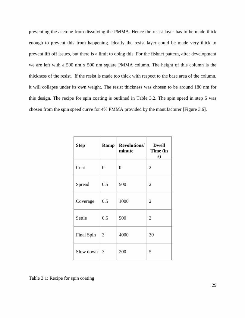
preventing the acetone from dissolving the PMMA. Hence the resist layer has to be made thick
enough to prevent this from happening. Ideally the resist layer could be made very thick to
prevent lift off issues, but there is a limit to doing this. For the fishnet pattern, after development
we are left with a 500 nm x 500 nm square PMMA column. The height of this column is the
thickness of the resist. If the resist is made too thick with respect to the base area of the column,
it will collapse under its own weight. The resist thickness was chosen to be around 180 nm for
this design. The recipe for spin coating is outlined in Table 3.2. The spin speed in step 5 was
chosen from the spin speed curve for 4% PMMA provided by the manufacturer [Figure 3.6].
Step
Ramp
Revolutions/
minute
Dwell
Time (in
s)
Coat
0
0
2
Spread
0.5
500
2
Coverage
0.5
1000
2
Settle
0.5
500
2
Final Spin
3
4000
30
Slow down
3
200
5
Table 3.1: Recipe for spin coating
30
Figure 3.6: Thickness as a function of spin speed for PMMA from MicroChem
The thickness of the resist layer was measured to be around 180 nm averaged over ten
measurements across randomly chosen points on the sample surface. Once the proper resist
thickness is determined, the lithography process follows. In a sense, electron beam lithography
(or EBL) is similar to photolithography.
The principle of EBL is in similar to photolithography in many respects. The surface of
the substrate has to be spin coated with an electron sensitive resist in EBL instead of a photo
sensitive one. A controlled electron beam then literally writes the pattern onto this resist. So no
mask is required like in photolithography.
Before any writing is done, a design has to be made. This design can be made in
AutoCAD and converted to a compatible GDSII file using LinkCAD, or the design software
provided by JEOL can be used to save the design as a J01 file. For relatively simple designs like

31
the fishnet, the pattern designer in the JEOL software is preferable, since the design conversion
step can be skipped. Following this, the GDSII or J01 file has to be converted to a v3.0 file
compatible with the EBL system, which essentially divides the design into fields and subfields
[Figure 3.7]. A field is like a unit cell, which when extended in the X and Y direction gives us
the whole pattern. Depending on the complexity of the design, the field can be further divided
into various subfields. Figure 3.8 illustrates the concept of a field using a simple schematic.
Figure 3.7: File conversion in the JEOL JBX 5500ZD

32
Figure 3.8: Schematic showing the concept of a field
The software searches for symmetry in the pattern and divides the entire pattern into
small fields. This is done because the sample stage moves in the following way: It exposes one
field to the electron beam, blanks the beam, steps to the next field, and exposes the same pattern.
Through this simple step and repeat process, the entire pattern is written. For example, for the
fishnet pattern the total patterned area was 1mm x 1mm with a field size of 180 μm x 180 μm.
Once the design is converted to a v3.0 file, the next step is system calibration. There are two
different calibration modes, either of which can be used for the JBX 5500ZD—the deflection
mode and the current mode. The deflection calibration mode was used for the fishnet pattern.
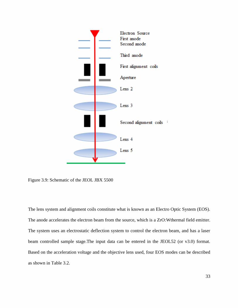
It is important to obtain a brief understanding of how the EBL system works. Figure
shows a simple schematic of the JBX 5500ZD system. Figure 3.9 shows a simple schematic that
can be used to understand the working principle of the JBX 5500ZD.
33
Figure 3.9: Schematic of the JEOL JBX 5500
The lens system and alignment coils constitute what is known as an Electro Optic System (EOS).
The anode accelerates the electron beam from the source, which is a ZrO:Wthermal field emitter.
The system uses an electrostatic deflection system to control the electron beam, and has a laser
beam controlled sample stage.The input data can be entered in the JEOL52 (or v3.0) format.
Based on the acceleration voltage and the objective lens used, four EOS modes can be described
as shown in Table 3.2.

34
Table 3.2: Operating modes of the JEOL JBX 5500ZD
The acceleration voltage can be chosen to be either 25 kV or 50 kV. For example, using a
lower acceleration voltage of 25 kV and lens 4 gives a maximum field size of 2000 µm, a
relatively high minimum scan step of 10 nm, with the advantage of the fastest writing speed. In
short, EOS Mode 1 is suitable for patterns of relatively larger critical dimensions, larger pitch
size, and in situations where writing speed is a priority. Using a higher acceleration voltage of 50
kV confines the electron beam to a smaller area, thus giving a smaller field size. Using lens 5
serves to focus the electron beam further for patterns of really small critical dimensions. This
comes at the disadvantage of a very small maximum field size, resulting in a very low writing
speed. For the fishnet pattern, the critical dimension was 80 nm–100 nm, it was sufficient to use
EOS Mode 2.
The major drawback of the EBL process is the time required to complete writing, even
while using EOS Modes 1 or 2. It can take up to two hours to complete writing a 1 mm x 1 mm
area, depending on the complexity of the design and step size of the beam. For the Fishnet

35
pattern the typical time required for writing was approximately 40 minutes for a 1 mm x 1mm
area. However for manufacturing on a commercial scale nanoimprinting techniques are available
that will be able to produce these cells at a much faster rate [64].
A 50 kV beam was used and the scan step was set to 2 nm to ensure that the pitch size
was accurate throughout the patterned area. After determining the appropriate EOS mode, the
next step is system calibration. In this step the electron beam is properly aligned and accurately
positioned with respect to the standard alignment marks (the AE and BE alignment marks). Also
the electron beam current can be adjusted during calibration. For the fishnet pattern the beam
current was adjusted to 1 nA, a standard value used with EOS mode 2. Adjusting the beam
current is the first step in sample alignment. Next, the position of the beam has to be accurately
determined. Every time a pattern is written, the system has to be calibrated. When the EOS mode
or filament current is changed, the system has to be calibrated. Every design will have a specific
set of acceleration voltage, lens, and filament current. This will affect the intensity and spot size
of the electron beam. The calibration process ensures that the beam spot accurately follows the
design saved in the input data file.
As mentioned earlier after writing one field the electron beam writes the next field. This
transition between fields takes place through a movement of the sample stage, thus making it
imperative for the stage control to be precisely controlled. Figure 3.10 shows a schematic for the
laser beam control for the sample stage in the JEOL 5500ZD.

36
Figure 3.10: Laser beam controlled sample stage of the JEOL JBX 5500ZD as described by
the equipment manual
For proper positioning of the sample stage, the system uses alignment markers known as
the AE and BE alignment marks. During the calibration process, the AE and BE marks have to
be located manually, focused, and their position has to be entered into the system. Based on these
values, the system performs a deflection correction, which ensures that there is minimum error
between the stage movement described by the software and the actual physical stage movement.
Figure 3.11 illustrates the deflection correction mechanism, as described by the manufacturers
user manual.
Pattern signal Electron beam
Deflector
A: Specified position
A’: Stop position Receiver
Mirror
Interferometer
Substrate
Stepper Motor
Stage
Deflection
amplifier
Signal
processor
Laser source A A’

37
Figure 3.11: Deflection correction in the JEOL JBX 5500ZD as described by the equipment
manual
The final step was exposure. The v3.0 file containing the design was loaded onto the
exposure window. This pattern has dimensions equal to the chip size of 180µm specified in the
design file, so it had to be laid out in a 6x6 two dimensional array to form a 1.08 mm x 1.08 mm
pattern. After the final array was made the exposure dose, scan step and calibration mode had to
be determined.
Electron beam
Deflector
Deflection width correction
BE mark BE mark
Stage Stage
Stage travel based on the laser distance measurement

38
The scan step is the step size of the beam and was fixed at 2 nm. The calibration mode, as
mentioned earlier, was set to deflection mode. The number of electrons incident on the resist per
square cm is defined as the dose. It is measured in μC/cm2. The dose has to be optimized for a
particular design. If the dose is too low, the intensity of the electron beam will not be enough to
expose the resist thoroughly. This condition is called “underexposure”. Also if the dose used is
too large, it results in the electron beam spreading laterally within the resist layer, thus widening
the feature size. This condition where the electron beam burns into the resist layer is called
“overexposure”. Determining the correct electron dose is only half the story. Similar problems of
residual resist or over etched resist can also be caused by an improper development process,
which will be discussed in due course.
For the fishnet structure was varied from 500 μC/cm2 to 1500 μC/cm2. The best results
were obtained for a dose of 800 μC/cm2. Basically obtaining a successful pattern is a
combination of the resist thickness, electron dose and development time. Once the exposure dose
is entered into the software the pattern is ready to be exposed on the substrate. After a writing
time that typically spanned 45 minutes for a 1mm x 1mm fishnet pattern, the sample was
unloaded and developed.
Development is defined as the process by which exposed resist is washed away by a
chemical known as a developer. This developer reacts selectively with regions that are exposed
to the electron beam and unexposed areas. The sample is usually dipped in a bath containing the
developer solution for a fixed time called the development time. The development time changes
depending on the design. If sufficient time is not allowed for development, the exposed resist is
left behind in clumps and the process is said to be “underdeveloped”. Similarly, when the sample

39
is kept dipped in the developer in excess of the development time, the developer starts to etch the
unexposed areas as well, thus widening the exposed features. In this case the process is said to be
“overdeveloped”.
The final development time for a 1 mm x 1 mm fishnet pattern was 25 seconds, given the
resist thickness and exposure dose. After development there was a fishnet shaped groove in the
PMMA layer. The sample was washed using IPA for 30 seconds to remove any residual
developer within the grooves and the sample was blown dry using nitrogen. Following this the
resist was baked at 100ºC on a hot plate for 60 seconds. This evaporates any moisture or organic
residues present in the sample, as well as it makes the PMMA columns more rigid structurally.
Care must be taken not to hard bake the resist on to the substrate, so as to prevent proper lift-off.
A period of 60-90 seconds is deemed appropriate according to the manufacturers data sheet
[Reference].
The next step was to evaporate metal onto the grooves to obtain a metallic fishnet
structure on the substrate. The sample was loaded onto a thermal evaporator. According to
design specifications, the thickness of the fishnet should be 20 nm, but it was found that thin
films of silver had issues adhering to the AZO surface. So a 7 nm layer of chromium was used
below the silver layer to promote adhesion. Once evaporation was completed a lift off had to be
performed

40
3.3 Measurement of Total Absorption of the Thin Film Solar Cell With and Without the
Fishnet Structure
After fabricating the sample, the next step is to measure the amount of light absorbed by
the sample. The sample has a metal back electrode; hence the transmission through the sample
will be practically zero. Under these circumstances, if the fishnet does indeed work as a
plasmonic scatterer, we should observe an increase in total absorption at the resonance
frequency. The reflection from the sample was measured using a Spectroscopic Ellipsometer.
Since transmission is negligible, we can safely assume that the rest of the light is absorbed by the
sample. There may be a concern here that the total absorption does not accurately represent the
power actually absorbed in the a-Si layer. It also includes the losses that take place in the fishnet
structure, AZO layers and the back electrode. In Chapter 4, results will be presented which prove
that as much as 83% of the total light absorption occurs within the a-Si layer. Thus it is correct to
measure the reflection off the top of the sample, and calculating transmission from it. For
reflection measurement a Variable Angle Spectroscopic Ellipsometer was used. Ellipsometry is a
widely used material characterization, and the measurement is essentially reflection based. Thus
it can also be used to measure reflection and transmission. Both the material characterization and
reflection measurement features have been used in this project.
The equipment is manufactured by the J. A. Woollam Company in Lincoln, Nebraska,
USA. Figure 3.10 shows a photograph of the V-VASE system installed at the Microwave and
Optics Laboratory for Imaging and Characterization, University of Arkansas.

41
(a) V-VASE system at the University of Arkansas, Fayetteville.
(b) Heat stage (c) Rotating stage
(d) Focus probes mounted on the source and detector units
Figure 3.12: Components of the V-VASE system from the J. A. Woollam Co. (Photograph by
Sayan Seal, July 12, 2013)
Detector Source Fiber
Optic
Mount
Vacuum
Pump
Sample
stage
Input focusing probe Output focusing probe

42
Apart from the sample stage shown in Figure 3.12 (a), the ellipsometer can also be
operated with a host of other stages like the heat stage for temperature dependent measurements
[Figure 3.12 (b)], and the rotating stage for anisotropic samples [Figure 3.12 (c)]. The source
ranges from 190 nm to 2500 nm, and can be varied in steps of 1 nm. The beam spot size is 0.5
cm when the alignment detector is present and 250 µm with the focusing probes mounted. Figure
(d) shows the focus probes mounted on the source and detector units. Since the fishnet was
fabricated on a 1mm x 1mm area, it was necessary to use the focus probes to shrink focus the
beam to a 250 µm spot within the fishnet area. Figure 3.13 shows the beam spot confined within
the area in which the fishnet pattern was fabricated. The picture shows the top view of a
complete fishnet solar cell structure. This patterned area appears as a dark square in the figure,
whereas the white square coincides with the area of the beam spot. The image was taken using a
camera mounted on the sample stage and operated using the JAW-Cam software.
Figure 3.13: Beam spot positioned within the fishnet pattern area (Photograph by Sayan Seal,
July 12, 2013)
43
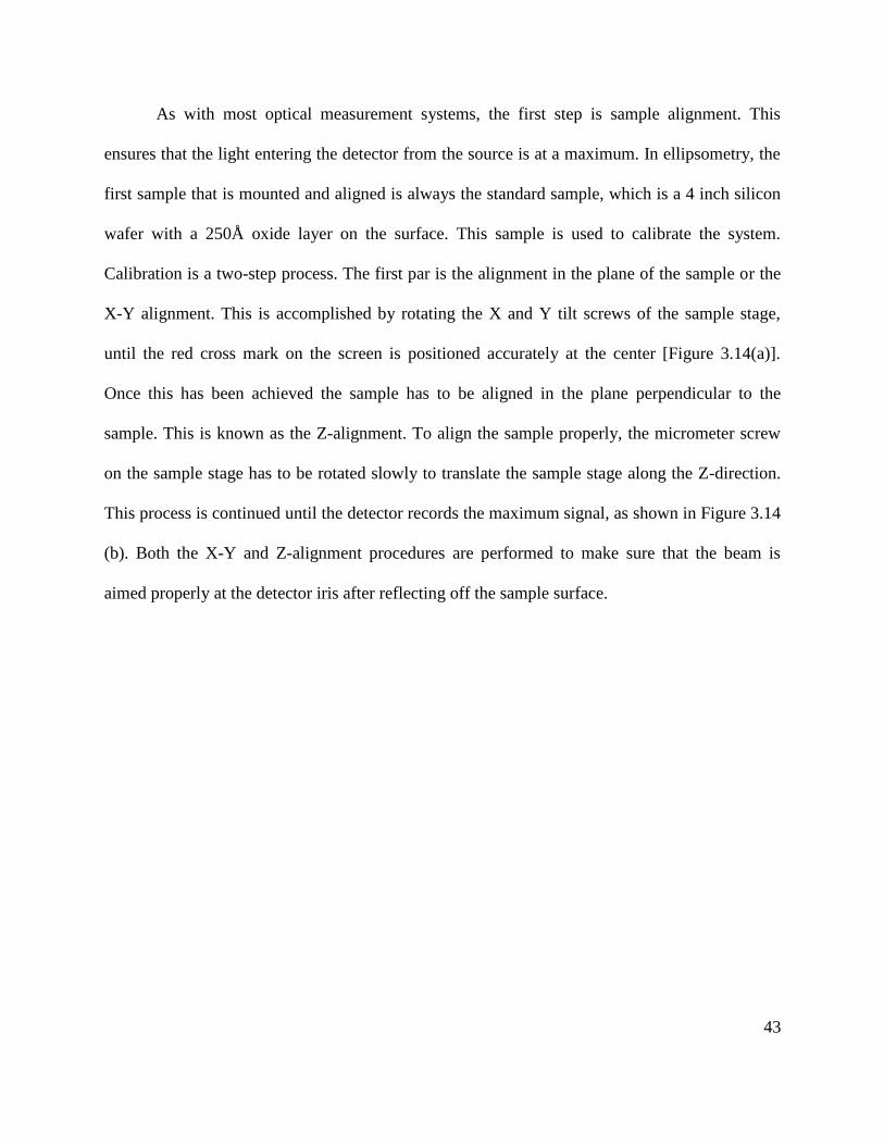
As with most optical measurement systems, the first step is sample alignment. This
ensures that the light entering the detector from the source is at a maximum. In ellipsometry, the
first sample that is mounted and aligned is always the standard sample, which is a 4 inch silicon
wafer with a 250Å oxide layer on the surface. This sample is used to calibrate the system.
Calibration is a two-step process. The first par is the alignment in the plane of the sample or the
X-Y alignment. This is accomplished by rotating the X and Y tilt screws of the sample stage,
until the red cross mark on the screen is positioned accurately at the center [Figure 3.14(a)].
Once this has been achieved the sample has to be aligned in the plane perpendicular to the
sample. This is known as the Z-alignment. To align the sample properly, the micrometer screw
on the sample stage has to be rotated slowly to translate the sample stage along the Z-direction.
This process is continued until the detector records the maximum signal, as shown in Figure 3.14
(b). Both the X-Y and Z-alignment procedures are performed to make sure that the beam is
aimed properly at the detector iris after reflecting off the sample surface.

44
(a): Screenshot of the X-Y alignment process in the WVASE software
(b) Screenshot of the Z-alignment process in the WVASE software
Figure 3.14: Alignment process for the V-VASE system

45
In ellipsometry the incident light is polarized in a direction either perpendicular to (s-
polarization) or parallel to (s-polarization) the plane of incidence. This makes it necessary for the
polarizers to be calibrated accurately before taking measurements. This step is known as system
calibration. In this step the standard sample is mounted and aligned, after which the system is
calibrated based on reflection obtained from the sample. The nature of reflected light is a known
quantity and the measurements obtained are fitted to these known results. If the resulting error is
less than the prescribed limit, sample calibration is successful. There will be issues with sample
alignment if the source intensity is too low. This is indicative of the fact that the alignment of the
source or sample (or both) is not satisfactory. Hence it is very important to get the alignment step
right before proceeding to calibration. Figure 3.15 shows the calibration data fits for the Fourier
coefficients α, β, and the residual function of the intensity of light on the detector.
Figure 3.15: Graph showing accurate fits between measured and fitted calibration data
46
It is important to note here that while using the focus probes, the probes have to be aligned and
calibrated separately. The focus probes should be installed only after the sample has been
aligned. Following this, the X-Y alignment screws on the source and detector mounts have to e
adjusted for maximum signal
After calibration, the system is ready for measurements. Material characterization andreflection
measurement will be discussed in detail in sections 3.3 A and 3.3 B respectively.
3.3(A): Material Characterization
As stated earlier, the incident light from the source is polarized. When this light hits the
sample surface, its state of polarization changes depending on the nature of the sample. The
ellipsometer measures this change in terms of two variables, Ψ and Δ. These ellipsometer
measures a quantity ρ, which can be expressed in terms of Ψ and Δ by the following relation,
Where, Rp and Rs are the reflection coefficients of p- and s- polarized light respectively. The brief
description of these polarization states will be given in due course. The values of Ψ and Δ are
measured as a function of wavelength and a mathematical model is constructed to fit a curve to
these data sets. This model has the optical constants and thickness of the layers of the sample as
input. Once a best fit model for a given data set is obtained, the optical constants can be
calculated.
tan( )p i
s
Re
R

47
3.3(B): Reflection Measurements Using an Ellipsometer
Reflection measurement using an ellipsometer consists of two parts. The first step is
called a “baseline” measurement, which essentially gives us a measure of the ambient light
present in excess of the signal from the source. The sample used for the baseline measurement
should be very well characterized for optical properties. The calibration sample was used as the
baseline sample for this experiment, and the results are presented in Figure 3.16. However, it is
not necessary to use the calibration sample for the baseline measurement. The only condition is
that the sample used for baseline measurement should be well characterized in terms of optical
properties. Figure 3.17 shows the fit of psi and delta for the standard sample. The mean square
error of the fit is 0.3919.
Figure 3.16: Baseline measurement for ambient light
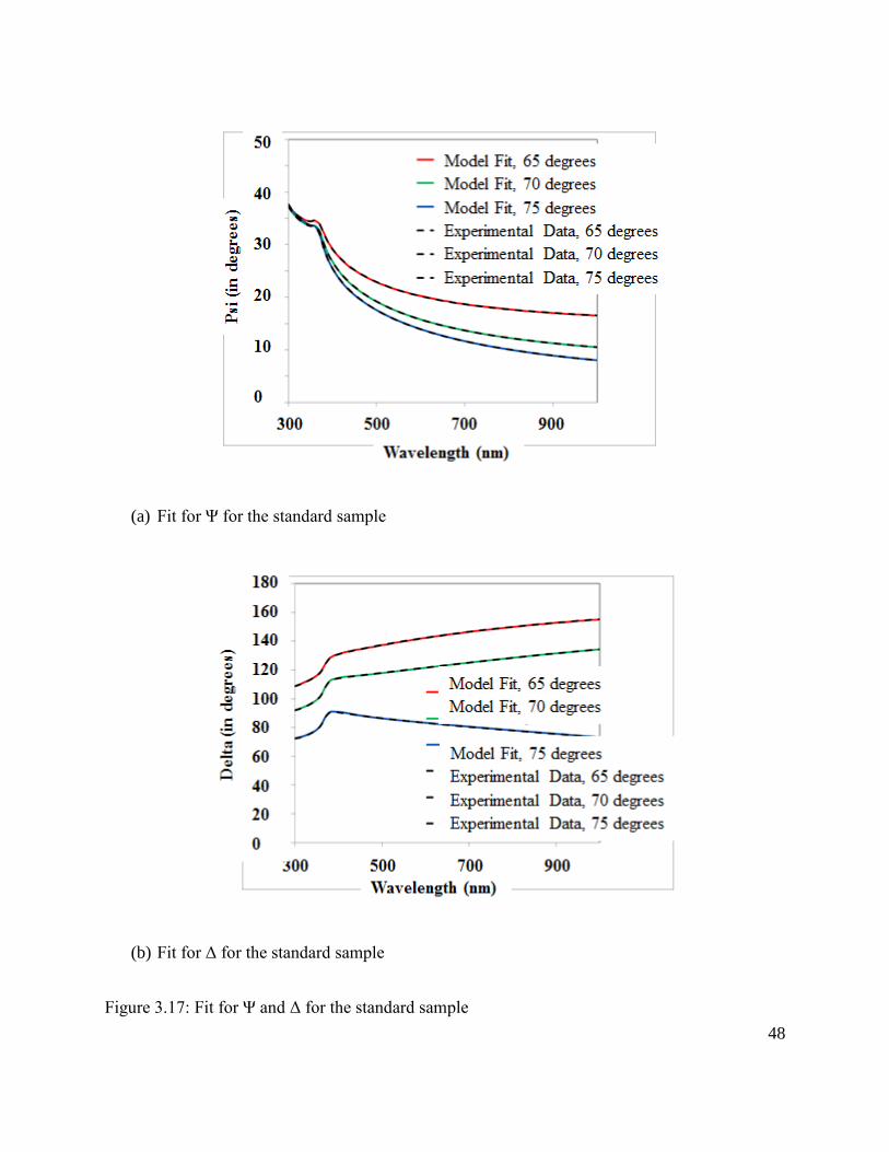
48
(a) Fit for Ψ for the standard sample
(b) Fit for Δ for the standard sample
Figure 3.17: Fit for Ψ and Δ for the standard sample

49
The angle of incidence for the baseline measurement has to be the identical to the angle
of incidence to be used for the actual sample. In addition, measurements should be taken at the
same wavelength points for the calibration sample and the actual sample. This is understandable
since the intensity of source is unique for a specified wavelength point, and this practice
facilitates correction for ambient light. The angle of incidence for reflection measurements was
kept fixed at 15⁰. Ideally the reflection at normal incidence should be measured, but 15⁰ is the
smallest angle of incidence achieved by the V-VASE system.
After the baseline measurement the Fishnet TFSC was mounted and aligned on the
sample stage. The reflection was measured and corrected using the baseline correction software
in the WVASE software. This changes the absolute reflection measured in random units into
reflectance, giving us the fraction of incident power that is reflected off the sample surface. The
transmission through the fishnet sample is negligible and is shown in Figure 3.18. Thus for all
practical purposes, the absorption can be expressed as (1 – Reflection).

50
Figure 3.18: Transmission through the fishnet TFSC
Four identical fishnet TFSC’s were fabricated to test the repeatability of the results
obtained above. This provides confirmation of two facts (i) the fabrication recipe is repeatable,
and (ii) The reflection measurement is accurate.
The measurement of reflection was done for three different states of polarization:
(i) p-polarization: When the electric field vector of light is parallel to the plane of
incidence, it is termed p-polarization.
(ii) s-polarization: When the electric field vector of light is perpendicular to the plane of
incidence, it is termed s-polarization.
51
(iii) u-polarization: When the electric field vector of light makes some specific anglewith
the plane of incidence, it is termed u-polarization. This is a user-defined angle that
can be changed in the WVASE software before taking measurements. It can range
from 0⁰ (p-polarized) and 90⁰ (s-polarized).
3.4 Modification of the Numerical Model and Comparison with Experimental Results
As a first step the different materials used to fabricate the Fishnet TFSC, namely, silver,
Al-doped zinc oxide, amorphous silicon and chromium were characterized for optical constants
using ellipsometry. Note that chromium was used as an adhesion layer below the silver fishnet,
but the original theoretical model did not take this into account. A 7 nm thick chromium fishnet
was created below the silver fishnet in the new model. For the characterization of these
materials, the following samples were used:
1) A 200 nm film of silver thermally evaporated on a silicon substrate
2) A 20 nm AZO film on a silicon substrate deposited by DC sputtering.
3) A 500 nm thick film of amorphous silicon deposited on a silicon substrate by Plasma
Enhanced Chemical Vapor deposition (PECVD) technique.
4) A 100 nm film of Cr deposited on a silicon substrate by thermal evaporation.
While fabricating the test samples, an effort was made to ensure that the following
parameters were kept identical with respect to the fabrication of the Fishnet TFSC,
1) Equipment used
52
2) Materials used
3) Thickness of deposited layers
After characterizing these materials, the optical constants obtained were used in HFSS
simulation to investigate whether it caused a better agreement between theory and experiment.
For the TFSC with fishnet, it was verified using Atomic Force Microscopy (AFM) that the AZO
layer covering the fishnet would not be flat, but would have a fishnet size bump over the area
where the fishnet was present. This factor was also considered in the numerical model in
conjunction with the ellipsometry-determined optical constants. The result of this numerical
simulation was compared to the experimental results.

53
Chapter 4: Results and Discussions
The results of the experimental procedures described in Chapter 3 will be presented in
this chapter, and will be presented in the same order in which the experiments were described. In
the first section, the results of numerical simulation will be presented. These will include plots
for total absorption, layer-wise absorption in the cell, and plots showing the electric field within
the a-Si layer. The results of the fabrication of the fishnet will be presented next, followed by the
third section in which the results of absorption measurement will be shown. The final section
consists of a comparison between the theoretical and experimental results, as well as a discussion
on making the results match better.
4.1. Design of the Thin Film Solar cell with a Fishnet Structure in the Back Spacer Layer
The design and simulation of the TFSC was done using the High Frequency Structure
Simulator (HFSS), a 3-D finite element simulation tool by Ansys, Inc. In this study, silver was
the chosen as the material for the fishnet and numerical optimizations were performed to obtain a
linewidth of 100 nm. Figure 3.1(a) shows the total absorption of the Fishnet TFSC plotted as a
function of wavelength, contrasted with the absorption from a planar TFSC without the fishnet.

54
(b) Total absorption of the TFSC with and without the Fishnet
(b) Layer-wise absorption in the TFSC with the Fishnet
Figure 4.1: Numerical simulation results of the fishnet solar cell in HFSS
0
0.1
0.2
0.3
0.4
0.5
0.6
0.7
0.8
0.9
1
400 500 600 700
Ab
sorp
tion
Wavelength (nm)
Total
a-Si
AZO front spacer
AZO back spacer
Fishnet
Ag back
55
It is important to note that increased total absorption does not amount to an increase in
absorption by the a-Si layer. It is the absorption in the a-Si layer that contributes to carrier
transport and enhances the electrical characteristics of the thin film solar cell. Hence it is
important to verify that the loss in the fishnet is low. So a complete layer-by-layer analysis of
absorption was done in HFSS, which verified that nearly 82% of the total absorption was in the
a-Si layer, with only 18% dissipated as loss in the fishnet, AZO and the silver back electrode
combined. The results of this analysis are presented in Figure 4.1(b).
Further proof of the fact that the fishnet structure results in an enhancement in absorption
in the a-Si layer is obtained by studying the electric field pattern within the absorber layer at the
resonance frequency. Figure 4.2 shows a comparison of the normalized electric field in the a-Si
layer with and without the fishnet. The simulation was done using HFSS. It was observed that
using the fishnet structure concentrates the electric field within the a-Si layer.

56
(a) with fishnet (b) without fishnet
Figure 4.2: Electric field in the a-Si layer of the fishnet TFSC computed using HFSS
At this point the design looked convincing enough to consider fabricating a complete thin
film solar cell structure. The principal challenge of making this structure was the fabrication of
the fishnet structure. The following sections will discuss the fabrication of the Fishnet TFSC in
greater detail.
Normalized
Electric Field
1.00
0.80
0.60
0.40
0.25
5.00e-3
Normalized
Electric Field
4.00e-2
3.00e-2
2.50e-2
1.75e-2
1.00e-2
1.58e-5

57
4.2 Fabrication of the Fishnet Pattern using Electron Beam Lithography
The optimized design for the silver Fishnet structure had a linewidth of 100 nm. It was
not possible to use photolithography since the system at the High Density Electronics Center
(HiDEC) at the University of Arkansas could do no less than 2.5 microns in terms of linewidth
given the design at hand. Hence Electron Beam Lithography (EBL) was used. The details of the
fabrication process have been explained in detail in Chapter 3. Pictures of the fishnet structure
were taken using Scanning Electron Microscopy (SEM). The images were taken after the lift off
step following metal deposition. The pictures show the top view of the silver fishnet on the
surface of the substrate.
Figure 4.3 shows the result obtained in the first trial. A dose of 1500 µC/cm2 was used
initially and the fishnet was patterned on a 550 nm thick layer of resist. A clean and uniform,
with no residues or defects pattern can be seen in the image. But the linewidth turned out to be
much larger than expected. An average linewidth of 200 nm was obtained, which was double
that in the design.

58
Figure 4.3: SEM pictures for a dose of 1500 μC/cm2 and a design linewidth of 100 nm
There were two factors that caused this:
(1) The dose was too high. This resulted in the lateral spreading of the electron beam in the resist
layer and resulted in an increase in the linewidth.
(2) The development time was longer than necessary. This causes the developer to etch in to the
sidewalls causing the linewidth to become wider.
An easy fix for this condition would be to reduce the design linewidth in the software, but
that would not give us an estimate of how close we could get to the targeted linewidth without
manipulating the design. So as a next step the dose was reduced to 1000 μC/cm2. Figure 4.4
shows the SEM picture of the pattern. It turns out that using a smaller dose ends up
underexposing the resist. The developer cannot wash away most of the exposed regions and
hence we get patches of silver when we evaporate metal onto the sample.

59
Figure 4.4: Using a smaller dose results in underdeveloped pattern
It was clear that we needed a smaller dose to achieve a smaller linewidth. One wayto do
this and ensure that the resist was adequately exposed was to make resist layer thinner. Hence a
4% solution of PMMA in anisole was used with a faster spin speed to get a thinner layer of
resist. The curve shown in Figure was used to determine the spin speed. It is observed that a
speed of about 4000 rpm would give a thickness of just under 200 nm. The same recipe
described in Table 3.1 was used, but the spin speed during final spin was changed to 4000 rpm.
The thickness averaged over ten measurements was found to be 180 nm.
Once again a dose of 1000 μC/cm2 was used, but this time the development time was
varied. Since the resist layer was thinner, lesser time would be required to wash off lesser
material during development. Three samples were fabricated and the development time was
reduced for each sample. The results are shown in Figure 4.5.

60
(a) Development time = 40 seconds (b) Development time = 35 seconds
(c) Development time = 30 seconds
Figure 4.5: Optimization of development time

61
A development time of 35 seconds worked best giving a linewidth of 115 nm. However
the linewidth was not uniform over the entire pattern and varied between 108 nm to 123 nm. 30
seconds gave narrower linewidths but regions around the corners showed signs of
underdevelopment [Figure 4.5(c)].
At this point the design linewidth of 100 nm in the software was reduced to counteract
the excess width on the fabricated sample. We were sufficiently close to 100 nm to be able to
take this step. After that it would just be a question of calibrating the dose and the recipe would
be ready. The design linewidth was reduced to 85 nm. The same dose of 1000 μC/cm2 but a
development time of 30 seconds was used. Note that the development time was also slightly
reduced. Due to the reduction in the design linewidth, the beam will expose lesser volume of
resist; hence we would require less time to wash off the exposed resist. The result of this process
is shown in Figure 4.6.
Figure 4.6: Design linewidth reduced to 85nm, development time reduced to 30 seconds

62
The linewidth obtained was still around 115 nm, but there was much more consistency in
the linewidth than before.
Lastly, a dose optimization was performed to get down to 100 nm. Keeping the design
linewidth and development time constant at 85 nm and 30 seconds respectively, the dose was
changed from 500 μC/ cm2 to 800 μC/ cm2 in steps of 100 μC/ cm2. From the results [Figure 4.7],
it can be observed that a dose of 800 μC/ cm2 gave an average linewidth of about 105 nm. Using
a dose smaller than this resulted in underexposure.

63
(a) Dose = 800 μC/ cm2 (b) Dose = 700 μC/ cm2
(c) Dose = 600 μC/ cm2 (d) Dose = 500 μC/ cm2
Figure 4.7: Final dose optimization step
At 700 nm the linewidth dropped below 100 nm, and for lower doses there were
problems of underexposure. At a dose of 800 nm, the recipe worked perfectly yielding a
linewidth of 105 nm on an average. It was expected that using a marginally shorter development
time could give us a perfect 100 nm linewidth. The best results were obtained using a

64
development time of 25 seconds [Figure 4.8]. The linewidth was found to be uniformly 100 nm
at the center of the pattern as well as the corners, with proper lift off across the entire patterned
area. Also a consistent pitch size of 598 nm was obtained.
(a) Linewidth = 100 nm (b) Pattern uniform over whole area
Figure 4.8: 100 nm linewidth pattern using a dose of 800 μC/ cm2, design linewidth of 85 nm,
and develop time of 25 seconds.
The above recipe was repeated on at least eight fishnets to make sure that a repeatable and
reliable fabrication process was developed. The SEM showed the same 100 nm linewidth for all
samples that were fabricated using the above recipe. Following the fabrication of the fishnet, the
rest of the steps in Figure 3.1 had to be completed to obtain a complete thin film solar cell
structure. 50 nm of AZO was deposited using DC sputtering, followed by 500 nm a-Si using
PECVD. The 50 nm AZO front spacer was deposited using DC sputtering as well. Thus the
fabricated structure optically resembled a thin film solar cell in all respects.

65
4.3 Measurement of Total Absorption of the Fabricated Samples
After a repeatable fabrication process for fabricating the fishnet solar cell was
established, the next step was to measure the absorption in this sample and determine whether
there is an enhancement. As a control sample a planar TFSC was used, i.e., a thin film solar cell
minus the fishnet. All other layers were the same and were of the same thickness as previously
described.
The details of the measurement method have been discussed in detail in Chapter 3. It is
worth mentioning here again that measuring reflection from the top surface is not a faithful
representation of total absorption. Figure 3.1 shows the layer-wise absorption in a Fishnet TFSC.
It was clearly established through numerical simulation in HFSS that 82% of the total absorption
occurs within the a-Si layer.
A 4 inch silicon wafer with a 250Å oxide layer on the surface was used to calibrate the
system. Following the calibration step the “baseline” measurement is performed to get a measure
of the ambient light present. The angle of incidence for the baseline measurement was kept fixed
at 15⁰. Measurement at normal incident would be ideal but 15⁰ is the smallest angle of incidence
that can be achieved by the V-VASE system.
After the baseline measurement the Fishnet TFSC was mounted and aligned on the sample stage.
The reflection was measured and corrected using the baseline correction software in the WVASE
software. The absorption spectrum if the Fishnet TFSC contrasted with a comparable planar
TFSC is shown plotted in Figure 4.9.We observe a 12.8x enhancement in total absorption near

66
the band gap of a-Si. There is also significant enhancement observed across the entire
wavelength range.
Figure 4.9: Comparison of total absorption with and without fishnet
Based on the absorption measurements, the short circuit current density JSC was computed
using Equation (4.2) and the results are presented in Table 4.3. The JSCis enhanced by 30% as a
result of including the fishnet in the back spacer.
Where,
e = Electronic charge
0
0.1
0.2
0.3
0.4
0.5
0.6
0.7
0.8
0.9
1
400 500 600 700
Ab
sorp
tion
Wavelength (nm)
Without Fishnet
With Fishnet
0( ) ( )SCJ eA d

67
A = Absorption in the a-Si layer
Φ = Number of incident photons per wavelength
S. No. TFSC Jsc(mA/cm2)
1. Without fishnet 11.751
2. With Fishnet 01 15.6553
3. With Fishnet 02 15.6775
4. With Fishnet 03 14.9136
5. With Fishnet 04 14.9464
Table 4.3: JSC comparison with and without the fishnet structure
Four identical Fishnet TFSC’s were fabricated to test the repeatability of the results
obtained above. Figure 4.10shows the absorption spectra of four Fishnet TFSC’s—Fishnet01,
Fishnet02, Fishnet03, and Fishnet 04. We observe almost identical patterns both with respect to
magnitude as well as in the positions at which the peaks occur. This provides confirmation of
two facts (i) the fabrication recipe is repeatable, and (ii) The reflection measurement is accurate.

68
Figure 4.10: Consistent results for measurements taken for four different samples
The measurement of reflection was done for three different states of polarization. The absorption
spectra corresponding to the three polarization states are shown in Figure 4.11. We observe that
the spectra correlate very well for all three polarizations. We can thus infer that the performance
of the Fishnet is independent of the state of polarization of the incident light.
0
0.1
0.2
0.3
0.4
0.5
0.6
0.7
0.8
0.9
1
400 500 600 700
Ab
sorp
tion
Wavelength (nm)
Fishnet 01
Fishnet 02
Fishnet 03
Fishnet 04

69
Figure 4.11: Measurements consistent for different polarization states
So far we have established that the Fishnet TFSC is successful in enhancing absorption in
the cell, hence doing exactly what it was designed to do. Figure 4.12 shows the comparison of
results obtained from numerical simulation versus the results obtained experimentally, both for
the case with and without the fishnet.
0
0.1
0.2
0.3
0.4
0.5
0.6
0.7
0.8
0.9
1
400 500 600 700
Ab
sorp
tion
Wavelength (nm)
p-polarization
s-polarization
u-polarization

70
(a) Without fishnet
(b) With fishnet
Figure 4.12: Comparison between numerical simulation and experimental results
0
0.1
0.2
0.3
0.4
0.5
0.6
0.7
0.8
0.9
1
400 500 600 700
Ab
sorp
tion
Wavelength (nm)
From Experiment
From HFSS using
Optical Constants from
Reference Data
0
0.1
0.2
0.3
0.4
0.5
0.6
0.7
0.8
0.9
1
400 500 600 700
Ab
sorp
tion
Wavelength (nm)
Experimental Result
HFSS with reference
optical constants
71
As we can observe, none of the plots show a good correlation between theory and
experiment. This was a worrying sign and meant that we exercised very little control over how
the fishnet structure actually behaved. Even though the end result was achieved, the disparity
between theory and experiment left a lot to be desired. The next part of this chapter gives a
detailed account of the steps taken to address these disparities.
4.4 Ellipsometric Characterization and Structural Modification of Numerical Model
The fabricated Fishnet TFSC showed an increase in the absorption as predicted by
numerical simulations: but the disparity between the absorption spectrum of the experimental
and simulated results could not be ignored. This essentially meant that we had no control over
how the structure behaved, and that we could not engineer these structures to perform exactly as
we wanted. Hence the obvious next step was to investigate the reason behind this deviation.
There could be two major reasons for the disparity observed between theory and experiment
1) The optical properties of the materials used to fabricate the Fishnet TFSC are not exactly
similar to the values used for numerical simulations in HFSS. The optical constants used in
HFSS simulations were taken from the database of SopraInc, and the optical constants for
AZO were taken from the Materion Company. The optical constants of materials are not
universally constant entities. They differ considerably depending on method of manufacture,
level of purity, quality of raw materials used, etc. Hence the optical response of an
experimental sample should logically be different from a theoretical model based on optical
constants derived from literature.

72
2) In the theoretical model, the interfaces of the different layers in the Fishnet TFSC are
assumed to be perfectly flat. However, that is never the case in reality. The surface roughness
associated with the interfaces can potentially contribute to a significant amount of scattering.
In this light we would like to stress on one particular instance of surface non-uniformity. The
AZO layer deposited on top of the 27 nm Fishnet is only 50 nm thick. Quite obviously this is
not going to be a flat surface, but a bumpy one. Hence we can see more scattering within the
a-Si layer as a result of this non-uniformity.
4.4.1 Effects of using Ellipsometry-determined Optical Constants in the Numerical Model
As a first step we had to characterize the different materials used to fabricate the Fishnet
TFSC, namely, silver, Al-doped zinc oxide, amorphous silicon and chromium. Note that
chromium was used as an adhesion layer below the silver fishnet, but the original theoretical
model did not take this into account. A 7 nm thick chromium fishnet was created below the silver
fishnet in the new model.
The optical constants that were extracted were as close as possible to the fabricated
TFSC. The results of this characterization were compared with reference values from literature
and are illustrated in Figure 4.13 through Figure 4.17. First, the substrate was characterized.

73
Figure 4.13: Silicon substrate
Figure 4.14: 100 nm film of silver on silicon substrate
5
4
3
2
1
0
300 400 500 600 700
k
Wavelength (nm)
Ellipsometry
Reference
8
7
6
5
4
3
2
1
0
300 400 500 600 700
Ellipsometry
Reference
n
Wavelength (nm)
1.8
1.6
1.4
1.2
1
0.8
0.6
0.4
0.2
0
n
Wavelength (nm)
Ellipsometry
Reference
300 400 500 600 700
6
5
4
3
2
1
0
300 400 500 600
700 Wavelength (nm)
(nm)
k
Ellipsometry
Reference

74
Figure 4.15: 100 nm chromium film on silicon substrate
Figure 4.16: 20 nm AZO on silicon substrate
n
Ellipsometry
Reference
3
2.5
2
1.5
1
0.5
0
300 400 500 600 700
0.8
0.7
0.6
0.5
0.4
0.3
0.2
0.1
0 300 400 500 600 700
k
Ellipsometry
Reference
Ellipsometry
Reference
n
4.5
4
3.5
3
2.5
2
1.5
1
0.5
0 400 500 600 700
Wavelength (nm)
400 500 600 700
Ellipsometry
Reference
k
4
3
2
1
0
Wavelength (nm)
Wavelength (nm) Wavelength (nm)

75
Figure 4.17 : 500 nm a-Si on silicon substrate
As we can observe the trend of variation of the optical constants is similar to the
reference data, but the magnitude is quite different. The optical constants determined from
ellipsometry were used as input variables in the theoretical model constructed in the HFSS
software. The structure was re-simulated across a wavelength range from 400 nm to 750 nm. The
absorption spectrum was plotted and compared with the case in which reference optical constants
were used. The results are presented in Figure 4.18.
6
5
4
3
2
1
0 300 400 500 600 700
n
Wavelength (nm)
(nm)
Ellipsometry
Reference
Ellipsometry
Reference
300 400 500 600 700
4
3.5
3
2.5
2
1.5
1
0.5
0
k
Wavelength (nm)
(nm)
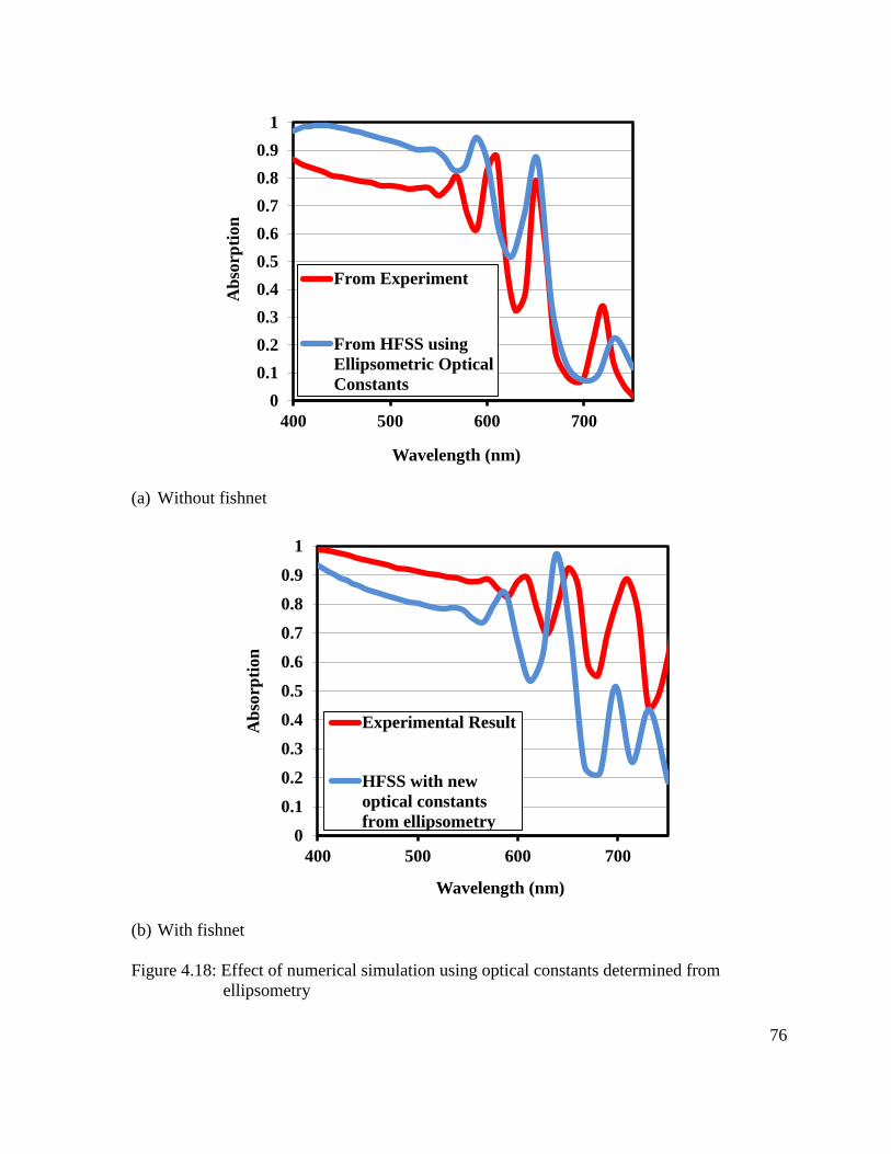
76
(a) Without fishnet
(b) With fishnet
Figure 4.18: Effect of numerical simulation using optical constants determined from
ellipsometry
0
0.1
0.2
0.3
0.4
0.5
0.6
0.7
0.8
0.9
1
400 500 600 700
Ab
sorp
tion
Wavelength (nm)
From Experiment
From HFSS using
Ellipsometric Optical
Constants
0
0.1
0.2
0.3
0.4
0.5
0.6
0.7
0.8
0.9
1
400 500 600 700
Ab
sorp
tion
Wavelength (nm)
Experimental Result
HFSS with new
optical constants
from ellipsometry
77
First, let us consider the case without the fishnet, i.e., a simple planar thin film solar cell
[Figure 4.14 (a)]. It was observed that using ellipsometric optical constants improved the
correlation between theory and experiment to a great extent. Using reference optical constants
instead causes the theoretically predicted absorption spectrum to deviate considerably from
experimental results.
With the fishnet in place, the absorption spectra using ellipsometric optical constants do a
better job of replicating the experimental data, but there is still significant disparity between
theory and experiment as far as the magnitude of absorption was concerned. This is the case for
both the 100 nm line width sample as well as the 150 nm line width sample. What was
encouraging was that the frequencies at which the maxima and minima in absorption occurred
matched up. This gives enough reason to suspect that if there are bumps and roughness
associated with the interfaces, the scattering (and consequently absorption) will be enhanced.
This will result in an even better match between theoretical and experimental results.
4.4.2 Structural Modifications in the Numerical Model
The first step in this exercise was to determine the source of surface non-uniformities that
could be responsible for enhancing the scattering. The major surface feature contributing to
surface irregularity is the fishnet itself. The silver fishnet, along with the chromium adhesion
layer below it, is 27 nm thick. Above this structure we deposit 50 nm AZO to enclose the fishnet
within the AZO back spacer. In the theoretical model in HFSS, the second AZO layer forms a
perfectly flat interface with the a-Si layer above. In reality, however, this is not the case.

78
When AZO is deposited over the fishnet the areas on top of the fishnet will already have a 27 nm
clearance from the bottom AZO layer. As we deposit more AZO, instead of being flat, the top
AZO layer will have bumps that will be approximately 27 nm high. This concept is explained
schematically in Figure 4.19 (a).
This was also verified experimentally by using Atomic Force Microscopy (AFM). The
same glass substrate was used, on which 50 nm AZO was deposited. The silver Fishnet along
with the chromium adhesion layer underneath was fabricated, and finally the second 50 nm AZO
layer was deposited on it. This sample was scanned by AFM to measure the height of the bump
on the surface of the Fishnet. The result of one such measurement is presented in Figure 4.19 (b).
It was seen that there is indeed a bump on the surface that measures up to exactly 27 nm on an
average.

79
(a) Schematic of bump over fishnet
(b) Result of AFM measurements taken over the fishnet structure
Figure 4.19: Structural modification used in the numerical model
27 nm AZO
bump over the
fishnet

80
After experimental verification, the next step was to include this feature in the theoretical
model and see if we can obtain a better correlation between theoretical and experimental results.
An AZO fishnet was embedded within the a-Si layer, above the AZO—a-Si interface. The rest of
the layers were kept the same. The result of this simulation is shown contrasted with
experimental results in Figure 4.20. Compared to Figure 4.12, the results are significantly better.
It can be observed that the new model comes very close to simulating the experimental results.
This is by far the best matching obtained between theory and experiment. It should also be noted
that the optical constants used for the new model were those determined from ellipsometry.
Figure 4.20: Result of including the bump on top of the fishnet in the numerical model
0
0.1
0.2
0.3
0.4
0.5
0.6
0.7
0.8
0.9
1
400 500 600 700
Ab
sorp
tion
Wavelength (nm)
HFSS
Ellipsometry

81
In this model the effect of surface roughness of the other layers was not considered. The
bump was believed to have a much greater impact on the nature of the absorption spectrum as
compared to minor features like surface roughness. However, including surface roughness could
further help enhance the absorption in the higher wavelength region. This will produce even
better correlation than what has been achieved so far. Also the angle of incidence in the
numerical simulation is 0º, but the ellipsometer used for the experiment can go down to only 15º.
This also accounts for the slight discrepancy we observe in the magnitude of absorption.

82
Chapter 5: Conclusions and Future Work
In this thesis it has been proved conclusively that the plasmonic fishnet structure
enhances the absorption in thin film solar cells. The fishnet structure was made of silver, had a
line width of 100 nm, pitch size of 600 nm, and a thickness of 20 nm. This design was tailored to
produce a plasmonic resonance at 680 nm, corresponding to the band gap of amorphous silicon.
The motive was to boost the absorption at this wavelength, which usually shows very low
absorption. There was a 13x increase in the absorption at the resonance frequency of 680 nm as a
result of including the fishnet in the back spacer layer of the solar cell. Moreover, it was proved
that 83% of this absorption occurs in the amorphous silicon layer. This translated to a 30%
increase in the calculated short circuit current density.
An accurate numerical model was also constructed that can be used to precisely monitor
he behavior of the fishnet structure. The significance of including the surface morphology of the
fishnet and the use of accurate optical constants has been illustrated. This is an important step
toward improving the efficiency of the thin film solar cells to enable them to compete better with
conventional wafer cells which dominate the world market today. The importance of developing
low cost high efficiency thin film solar cells as a means of cheap sustainable energy cannot be
stressed enough.
The future work in this project has two tracks. On the one hand, work is in progress to
fabricate a solar cell device. We are collaborating with Dr. Vikram Dalal’s group at the Iowa
State University to deposit a p-i-n structure. Secondly, efforts are under way to fabricate a fishnet
structure using Shape Memory Alloy materials like alloys of nickel an titanium. SMA materials
can be trained to change shape when subject to thermal stress, only to change back to its original

83
form once the applied stress has been removed. Since the plasmonic resonance frequency of the
fishnet depends on the geometry, it is possible to shift the resonance in our favor by using SMA
materials. One application of this concept would be to counteract the temperature induced
degradation in performance of solar cells. With increasing temperature, the SMA fishnet could
change dimensions and provide a resonance at the frequencies that are worst affected, only to
resume normal operation once the temperatures drop. Once these concepts have been illustrated
on test samples, the fabrication of plasmonic patterns like the fishnet can be scaled up to meet the
needs of the industry. Nanoimprinting techniques have been developed that can be used to print
these patterns as part of an assembly line or roll to roll manufacture techniques [75].

84
References
[1] http://www.economist.com/blogs/graphicdetail/2012/12/daily-chart-19
[2] http://keithhennessey.com/2012/03/12/nearly-doubling-renewable-energy-generation/
[3] Mints, P. and Donnelly, J., “Photovoltaic Manufacturer Shipments, Capacity and Competitive
Analysis 2010/2011,” Navigant Solar Services Program. Palo Alto, CA, 2011.
[4] Goodrich, A., James, T. and Woodhouse, M., “Solar PV Manufacturing Cost Analysis: U.S.
Competitiveness in a Global Industry,” available on NREL website:
http://www.nrel.gov/docs/fy12osti/53938.pdf
[5] A. Shah, P. Torres, R. Tscharner, N. Wyrsch and H. Keppner, “Photovoltaic Technology:
The Case for Thin-Film Solar Cells”, 30 July, 1999, Vol 285, Science.
[6] Kannan Ramanathan, Miguel A. Contreras, Craig L. Perkins, Sally Asher, Falah S. Hasoon,
James Keane, David Young, Manuel Romero, Wyatt Metzger, Rommel Noufi, James Ward and
Anna Duda, “Properties of 19.2% Efficiency ZnO/CdS/CuInGaSe2 Thin-film Solar Cells”, Prog.
Photovolt: Res. Appl. 2003; 11:225–230 (DOI: 10.1002/pip.494).
[7] Philip Jackson, Dimitrios Hariskos, Erwin Lotter, Stefan Paetel, Roland Wuerz, Richard
Menner, Wiltraud Wischmann and Michael Powalla, “New world record efficiency for
Cu(In,Ga)Se2 thin-film solar cells beyond 20%”, Prog. Photovolt: Res. Appl. 2011; 19:894–897.
[8] Schmela, M., Kruitmann, A., Photon Int., vol. 4, 38, 2002.
[9] NREL, Cadmium Use in Photovoltaics 2005, www.nrel.gov/cdte/perspective.html
[10] Schmela, M., Photon Int. January issue, vol. 1, 22–24, 2003.
[11] Yang, J. C., “Advances in amorphous silicon alloy technology—the achievement of high
efficiency multijunction solar cells and modules”, Prog. Photovoltaics 1998, 6, 181–186.
[12] Shah, A. V.; Schade, H.; Vanecek, M.; Meier, J.; Vallat-Sauvain, E.; Wyrsch, N.; Kroll, U.;
Droz, C.; Bailat, J., “Thin-film silicon solar cell technology”, Prog. Photovoltaics 2004, 12, 113
142.
[13] Schropp, R. E. I., Zeman, M., “Amorphous and Microcrystalline Silicon Solar Cells:
Modeling, Materials, and Device Technology”, Kluwer Academic Publishers: Boston, MA,
1998.

85
[14] D. L. Staebler, and C. R. Wronski, “Reversible conductivity changes in discharge-produced
amorphous silicon,” Appl. Phys. Lett. 31(4), 292–294 (1977).
[15] A. V. Shah, H. Schade, M. Vanecek, J. Meier, E. Vallat-Sauvain, N. Wyrsch, U. Kroll, C.
Droz, and J. Bailat, “Thin-film Silicon Solar Cell Technology,” Prog. Photovolt. Res. Appl.
12(23), 113–142 (2004).
[16] http://sharp-world.com/corporate/news/130614.html
[17] Green, M. A., “Thin-film solar cells: review of materials, technologies and commercial
status,” J Mater Sci: Mater Electron, vol. 18, S15-S19, 2007
[18] Tool, C.J.J., Burgers, A.R., Manshanden, P. and Weeber, A.W., “Effect of Wafer Thickness
on the Performance Of mc-Si Solar Cells,” 17th European Photovoltaic Solar Energy
Conference, Munich, 2001.
[19] Beaucarne, G., “Silicon Thin-Film Solar Cells,” Adv. OptoElectronics, vol. 10, 1155-1166,
2007.
[20] Fonash, S.J., “Solar cell device physics, 2nd ed.,” Academic Press, 2010.
[21] PV Education, http://www.pveducation.org/pvcdrom
[22] Yablonovitch, E., “Statistical Ray Optics,” J. Opt. Soc. Am., vol. 72, no. 7, pp. 899-907,
1982.
[23] Yablonovitch, E. and Cody, G. D., “Intensity Enhancement in Textured Optical Sheets for
Solar Cells,” IEEE. Trans. Elctron Dev., vol. E-29, no. 2, 300-305, 1982.
[24] Liming Ji, “Plasmonic and photonic designs for light trapping in thin film solar cells”,
University of Arkansas, ProQuest, UMI Dissertations Publishing, 2012. 3541937.
[25] Asahi glass company
http://www.agc.com/english/csr/environment/products/positive_seihin1.html
[26] Loffler, J., Groenen, R., Linden, J. L., van de Sanden, M. C. M, Schropp, R. E. I.,
“Amorphous silicon solar cells on natively textured ZnO grown by PECVD,” Thin Solid Films,
vol. 392, 315-319, 2001.
[27] Groenen, R., Loffler, J., Sommeling, P.M., Linden, J. L., Hamers, E. A. G., Schropp, R. E. I.
and van de Sanden, M.C.M., “Surface textured ZnO films for thin film solar cell applications by
expanding thermal plasma CVD,” Thin Solid Films, vol. 392, 226-230, 2001.

86
[28] Zeman, M., van Swaaij, R. A. C. M. M., Metselaar, J. W. and Schropp, R. E. I., “Optical
modeling of a-Si:H solar cells with rough interfaces: Effect of back contact and interface
roughness,” J. Appli. Phys., vol. 88, no. 11, 6426-6443, 2000.
[29] J. Krč, F. Smole, and M. Topič, “Potential of light trapping in microcrystalline silicon solar
cells with textured substrates,” Prog. Photovolt. Res. Appl. 11(7), 429–436 (2003).
[30] O. Kluth, B. Rech, L. Houben, S. Wieder, G. Schöpe, C. Beneking, H. Wagner, A. Löffl,
H.W. Schock, “Texture etched ZnO:Al coated glass substrates for silicon based thin film solar
cells”, “Thin Solid Films”, Elsevier, Volume 351, Issues 1–2, 30 August 1999, Pages 247–253.
[31] M. Berginski, J. Hüpkes, W. Reetz, B. Rech, M. Wuttig, “The effect of front ZnO:Al
surface texture and optical transparency on efficient light trapping in silicon thin-film solar
cells”, JAP, Volume:101 , Issue: 7 , Apr 2007, 074903 - 074903-11.
[32] J. Springer, B. Rech, W. Reetz, J. Muller, M. Vanecek, “Light trapping and optical losses in
microcrystalline silicon pin solar cells deposited on surface-textured glass/ZnO substrates,” Solar
Energy Materials & Solar Cells 85 (2005) 1–11.
[33] J. Hupkesa, B. Recha, O. Klutha, T. Repmanna, B. Zwaygardta, J. Mullera, R. Dreseb, M.
Wuttig, “Surface textured MF-sputtered ZnO films for microcrystalline silicon-based thin-film
solar cells,” Solar Energy Materials & Solar Cells 90 (2006) 3054–3060.
[34] Yu, Z., Raman, A. & Fan, S. Fundamental limit of nanophotonic light trapping
in solar cells. Proc. Natl Acad. Sci. 107, 17491–17496 (2010).
[35] Zhu, J., Hsu, C. M., Yu, Z., Fan, S. and Cui, Y., “Nanodome Solar Cells with Efficient
Light Management and Self-Cleaning,” Nano Lett., vol. 10, 1979-1984, 2010.
[36] Nam, W. J., Ji, L., Benanti, T. L., Varadan, V. V., Wagner, S., Wang, Q., Nemeth, W.
Neidich, D., and Fonash, S. J., “Incorporation of a light and carrier collection management
nanoelement array into superstrate a-Si:H solar cells,” Appl. Phys. Lett., vol. 99, no. 073113,
2011.
[37] Claus Heine and Rudolf H. Morf, “Submicrometer Gratings for Solar Energy Applications”,
Applied Optics, Vol. 34, Issue 14, pp. 2476-2482 (1995).
[38] C. Haase and H. Stiebig, “Optical Properties of Thin-film Silicon Solar Cells with Grating
Couplers,” Prog. Photovolt: Res. Appl. 2006; 14:629–641
[39] Lee, Y. J.; Ruby, D. S.; Peters, D. W.; McKenzie, B. B.; Hsu, J. W. P., “ZnO nanostructures
as efficient antireflection layers in solar cells,” Nano Lett. 2008, 8, 1501–1505.

87
[40] Soderstrom, T.; Haug, F. J.; Terrazzoni-Daudrix, V.; Ballif, C. J., “Flexible micromorph
tandem a-Si/μc-Si solar cells,” Appl. Phys. 2008, 103, 114509.
[41] Python, M.; Vallat-Sauvain, E.; Bailat, J.; Donine, D.; Fesquet, L.; Shah, A.; Ballif, C. J.,
“Microcrystalline silicon solar cells: effect of substrate temperature on cracks and their role in
post-oxidation,” Non-Cryst. Solids. 2008, 354, 2258.
[42] Boccard, M.; Cuony, P.; Despeisse, M.; Domine, D.; Feltrin, A.; Wyrsch, N.; Ballif, C. Sol.
Energy Mater. Sol. Cells 2011, 95, 195.
[43] Lohmuller, T.; Helgert, M.; Sundermann, M.; Brunner, R.; Spatz, J. P., “Biomimetic
Interfaces for High-Performance Optics in the Deep-UV Light Range,” Nano Lett. 2008, 8,
1429–1433.
[44] Barnes, W. L.; Dereux, A.; Ebbesen, T. W., “Surface plasmon subwavelength optics,”
Nature 2003, 424, 824–830.
[45] Barry, P. R.; Peter, P.; Stephen, R. F., “Three-Dimensional Nanoarchitectures: Designing
Next-Generation Devices”, J. Appl. Phys. 2004, 96, 7519–7526.
[46] Catchpole, K. R.; Polman, “Plasmonic solar cells,” A. Opt. Express 2008, 16, 21793–21800.
[47] Derkacs, D.; Lim, S. H.; Matheu, P.; Mar, W.; Yu, E. T., “Improved performance of
amorphous silicon solar cells via scattering from surface plasmon polaritons in nearby metallic
nanoparticles,” Appl. Phys. Lett. 2006, 89, No. 093103.
[48] Pillai, S.; Catchpole, K. R.; Trupke, T.; Green, M. A., “Surface plasmon enhanced silicon
solar cells,” J. Appl. Phys.2007, 101, No. 093105.
[49] Schuller, J. A., Barnard, E. S., Cai, W. S., Jun, Y. C., White, J. S. & Brongersma, M. L.
Plasmonics for extreme light concentration and manipulation. Nat. Mater. 9, 193–204 (2010).
[50] Atwater, H. A. & Polman, A. Plasmonics for improved photovoltaic devices. Nat. Mater. 9,
205–213 (2010).
[51] Nakayama, K., Tanabe, K. and Atwater, H. A., “Plasmonic nanoparticle enhanced light
absorption in GaAs solar cells,”Appl. Phys. Lett., vol. 93, no. 121904, 2008.
[52] Schaadt, D. M. and Yu, E. T., “Enhanced semiconductor optical absorption via surface
plasmon excitation in metal nanoparticles,” Appl. Phys. Lett., vol. 86, no. 063106, 2005.
[53] Katherine A. Willets and Richard P. Van Duyne, “Localized Surface Plasmon
Resonance Spectroscopy and Sensing”, Annu. Rev. Phys. Chem. 2007.58:267-297.
88
[54] Alexandre G. Brolo, Reuven Gordon, Brian Leathem, and Karen L. Kavanagh, “Surface
Plasmon Sensor Based on the Enhanced Light Transmission through Arrays of Nanoholes in
Gold Films”, Langmuir 2004, 20, 4813-4815.
[55] Maier, S. A. Plasmonics - Fundamentals and Applications, 1st ed.;
Springer: New York, 2007.
[56] William L. Barnes, Alain Dereux & Thomas W. Ebbesen, “Surface plasmon subwavelength
optics”, Nature, Vol 424 14, August 2003, 824-830.
[57] Otto, A. Exitation of nonradiative surface plasma waves in silver by the method of
frustrated total reflection. Z. Phys.216, 398 (1968).
[58] Ditlbacher, H. et al. Fluorescence imaging of surface plasmon fields. Appl. Phys. Lett. 80,
404–406 (2002).
[59] Ritchie, R. H., Arakawa, E. T., Cowan, J. J. & Hamm, R. N. Surface-plasmon resonance
effect in grating diffraction. Phys. Rev. Lett. 21, 1530–1533 (1968).
[60] Stefan A. Maier, Steve R. Andrews, L. Martin-Moreno, and F. J. Garcia-Vidal, “Terahertz
Surface Plasmon-Polariton Propagation and Focusing on periodically Corrugated Metal Wires”,
PRL 97, 176805 (2006).
[61] Liming Ji and Vasundara V. Varadan, “Fishnet metastructure for efficiency enhancement of
a thin film solar cell”, Journal Of Applied Physics 110, 043114 (2011).
[62] Zhang, S. et. al., “Near-infrared double negative metamaterials,” Opt. Express, vol.13,
4922-4930, 2005.
[63] Valentine, J., Zhang, S., Zentgraf, T., Ulin-Avila, E., Genov, D.A., Bartal, G. and Zhang,
X., “Three-dimensional optical metamaterial with a negative refractive index,” Nature, vol. 455,
376-379, 2008.
[64] Varadan, V.V., Tellakula, Anilkumar R., “Effective properties of split-ring resonator
metamaterials using measured scattering parameters: Effect of gap orientation”, Journal of
Applied Physics (Volume:100 , Issue: 3 ), Aug 2006 034910 - 034910-8.
[65] V. Varadan, L. Ji, “Optical Metastructures for Trapping Light in Thin Silicon Solar Cells”,
Proceedings of the 35th IEEE Photovoltaics Specialists Conference (PVSC) 2010, 001057
001059.
[66] Vivian E. Ferry, Marc A. Verschuuren, Hongbo B. T. Li, Ewold Verhagen, Robert J.
Walters, Ruud E. I. Schropp, Harry A. Atwater, and Albert Polman, “Light trapping in ultrathin
89
plasmonic solar cells”, Optics Express, Volume: 18, Issue: S2 (2010), pp. A237-A245.
[67] Vivian E. Ferry , Luke A. Sweatlock, Domenico Pacifici and Harry A. Atwater,
“Plasmonic Nanostructure Design for Efficient Light Coupling into Solar Cells”, Nano
Lett., 2008, 8 (12), pp 4391–4397.
[68] Bhattacharya, J.; Chakravarty, N.; Pattnaik,S.; Dennis Slafer,W. ; Biswas,Rana ;
Dalal,V.L.; “A photonic-plasmonic structure for enhancing light absorption in thin filmsolar
cells”, Appl. Phys. Lett. 99, 131114 (2011); doi: 10.1063/1.3641469.
[69] C. Battaglia et al, “Nanoimprint Lithography for High-Efficiency Thin-Film Silicon Solar
Cells”, Nano Lett., 2011, 11 (2), pp 661–665.
[70] C Min, J Li, G Veronis, JY Lee, S Fan, “Enhancement of optical absorption in thin-film
organic solar cells through the excitation of plasmonic modes in metallic gratings”, Applied
Physics Letters (Volume:96 , Issue: 13 ), March 2010, 133302 - 133302-3.
[71] Ragip A. Pala, John S. Q. Liu, Edward S. Barnard, Daulet Askarov, Erik C. Garnett,
Shanhui Fan & Mark L. Brongersma, "Optimization of non-periodic plasmonic light-trapping
layers for thin-film solar cells", Nature Communications, 4, 2095 (2013).
[72] Hairen Tan, Rudi Santbergen , Arno H. M. Smets , and Miro Zeman, “Plasmonic Light
Trapping in Thin-film Silicon Solar Cells with Improved Self-Assembled Silver Nanoparticles”,
Nano Lett., 2012, 12 (8), pp 4070–4076.
[73] Hummel, R. E., “Electronic Properties of Materials, 3rd ed,” Springer, 2000.
[74] Johnson, P. B. and Christy, R. W. “Optical constants of the noble metals,” Phys. Rev. B,
vol.6 4370-4379, 1972.
[75] Chia-Ching Liang, Mei-Yi Liao, Wen-Yu Chen, Tsung-Chieh Cheng, Wen-Huei Chang,
and Chun-Hung Lin, “Plasmonic metallic nanostructures by direct nanoimprinting of gold
nanoparticles”, Optics Express, Vol. 19, Issue 5, pp. 4768-4776 (2011).

90
Appendix 1: License for Figure 2.1
Permission on following page.

91

92

93

94

1

1

2