Design and Verification of Digital Architecture of 65K ...
110
CERN-THESIS-2010-123 07/10/2010 Design and Verification of Digital Architecture of 65K Pixel Readout Chip for High-Energy Physics Diplomity¨ o Turun yliopisto Informaatioteknologian laitos Tietokonej¨ arjestelm¨ at 2010 Tuomas Poikela Tarkastajat: Tomi Westerlund Jani Paakkulainen
Transcript of Design and Verification of Digital Architecture of 65K ...

CER
N-T
HES
IS-2
010-
123
07/1
0/20
10
Design and Verification of Digital
Architecture of 65K Pixel Readout Chip
for High-Energy Physics
DiplomityoTurun yliopistoInformaatioteknologian laitosTietokonejarjestelmat2010Tuomas Poikela
Tarkastajat:Tomi WesterlundJani Paakkulainen

TURUN YLIOPISTOInformaatioteknologian laitos
TUOMAS POIKELA: Design and Verification of Digital Architecture of 65K Pixel Read-out Chip for High-Energy Physics
Diplomityo, 89 s., 7 liites.TietokonejarjestelmatLokakuu 2010
Tassa tutkielmassa tarkastellaan voidaanko IBM:n 130 nanometrin CMOS-prosessia japrosessin standardisolukirjastoa kayttaa CERNin LHCb-kokeen VELO-ilmaisimen etu-paan sovelluskohtaisen integroidun piirin suunnitteluun ja toteutukseen.Tassa tyossa esitellaan arkkitehtuuri, joka on suunniteltu jatkuvaan tiedon keraykseenkorkeilla kaistanleveyksilla. Arkkitehtuuri on suunniteltu toimimaan ilman ulkoistaheratesignaalia ja sen on tallennettava tiedot jokaisesta hiukkastormayksesta ja lahetettavane eteenpain ilmaisimen seuraavalle elektroniikkatasolle, esimerkiksi FPGA-piireille.Tutkielmassa keskitytaan piirin aktiivisen alueen digitaalilogiikan suunnitteluun,toteutukseen ja oikeellisuuden varmentamiseen. Digitaalisen osion vaatimuksetasettavat pikseleiden geometriaan sidottu pinta-ala (55µm x 55µm), 10 piiriasisaltavan moduulin kokonaistehonkulutus (20 W/moduuli), jota rajoittavat moduulinjaahdytysmahdollisuudet, seka korkea ulostulevan tiedon maara (> 10 Gbit/s), joka ai-heutuu piirin lapi kulkevasta hiukkasvuosta.Tyon toteuksessa kaytettiin tapahtumatason mallinnusta SystemVerilogilla seka avoimenlahdekoodin verifiointikirjastoa OVM:a arkkitehtuurin optimointiin ennen RTL-toteutustaja piirisynteesia. OVM:a kaytettiin myos RTL-toteutuksen toiminnallisuuden oikeelli-suuden varmentamiseen kattavuuteen perustuvaa varmentamismetodologiaa noudattaen.
Asiasanat: ASIC, OVM, SystemVerilog, pikseli-ilmaisin, verifiointi, CERN

UNIVERSITY OF TURKUDepartment of Information Technology
TUOMAS POIKELA: Design and Verification of Digital Architecture of 65K Pixel Read-out Chip for High-Energy Physics
Master of Science in Technology Thesis, 89 p., 7 app. p.Computer SystemsOctober 2010
The feasibility to design and implement a front-end ASIC for the upgrade of the VELOdetector of LHCb experiment at CERN using IBM’s 130nm standard CMOS process anda standard cell library is studied in this thesis.The proposed architecture is a design to cope with high data rates and continuous datataking. The architecture is designed to operate without any external trigger to record everyhit signal the ASIC receives from a sensor chip, and then to transmit the information tothe next level of electronics, for example to FPGAs.This thesis focuses on design, implementation and functional verification of the digitalelectronics of the active pixel area. The area requirements are dictated by the geometryof pixels (55µm x 55µm), power requirements (20 W/module) by restricted cooling capa-bilities of the module consisting of 10 chips and output bandwidth requirements by datarate (> 10 Gbit/s) produced by a particle flux passing through the chip.The design work was carried out using transaction level modeling with SystemVerilogand Open Verification Methodology (OVM) to optimize and verify the architecturebefore starting RTL-design and synthesis. OVM was also used in functional verificationof the RTL-implementation following coverage-driven verification process.
Keywords: ASIC, OVM, SystemVerilog, pixel detector, verification, CERN

Contents
List of Figures v
List of Tables vii
List Of Acronyms viii
1 Introduction 1
2 Hybrid Pixel Detectors 3
2.1 Detector Hardware . . . . . . . . . . . . . . . . . . . . . . . . . . . . . 3
2.1.1 Silicon Sensor . . . . . . . . . . . . . . . . . . . . . . . . . . . 3
2.1.2 Readout Chip Floorplan . . . . . . . . . . . . . . . . . . . . . . 4
2.1.3 Analog Front-end . . . . . . . . . . . . . . . . . . . . . . . . . . 5
2.1.4 Digital Front-end . . . . . . . . . . . . . . . . . . . . . . . . . . 6
2.1.5 Readout Architectures . . . . . . . . . . . . . . . . . . . . . . . 6
2.2 Detector Concepts . . . . . . . . . . . . . . . . . . . . . . . . . . . . . . 7
2.2.1 Charge Sharing . . . . . . . . . . . . . . . . . . . . . . . . . . . 8
2.2.2 Time Over Threshold . . . . . . . . . . . . . . . . . . . . . . . . 8
2.2.3 Time Walk . . . . . . . . . . . . . . . . . . . . . . . . . . . . . 9
2.2.4 Peaking Time . . . . . . . . . . . . . . . . . . . . . . . . . . . . 9
2.2.5 Hit Rate, Dead Time and Efficiency . . . . . . . . . . . . . . . . 10
2.3 Radiation and Fault Tolerance . . . . . . . . . . . . . . . . . . . . . . . 11

2.3.1 Single Event Upsets . . . . . . . . . . . . . . . . . . . . . . . . 11
2.3.2 Triple Modular Redundancy . . . . . . . . . . . . . . . . . . . . 11
3 SystemVerilog and Open Verification Methodology 14
3.1 SystemVerilog . . . . . . . . . . . . . . . . . . . . . . . . . . . . . . . . 14
3.1.1 Classes and Structs . . . . . . . . . . . . . . . . . . . . . . . . . 15
3.1.2 Dynamic and Associative Arrays and Queues . . . . . . . . . . . 16
3.1.3 Mailboxes . . . . . . . . . . . . . . . . . . . . . . . . . . . . . . 17
3.2 Transaction Level Modeling . . . . . . . . . . . . . . . . . . . . . . . . 17
3.2.1 Abstract Models . . . . . . . . . . . . . . . . . . . . . . . . . . 18
3.2.2 Initiator and Target . . . . . . . . . . . . . . . . . . . . . . . . . 19
3.2.3 Blocking and Nonblocking Communication . . . . . . . . . . . . 21
3.3 Open Verification Methodology . . . . . . . . . . . . . . . . . . . . . . 22
3.3.1 OVM Testbench Architecture . . . . . . . . . . . . . . . . . . . 22
3.3.2 Components . . . . . . . . . . . . . . . . . . . . . . . . . . . . 24
3.3.3 Configuration . . . . . . . . . . . . . . . . . . . . . . . . . . . . 24
3.3.4 Sequences . . . . . . . . . . . . . . . . . . . . . . . . . . . . . . 25
3.3.5 Agent . . . . . . . . . . . . . . . . . . . . . . . . . . . . . . . . 25
4 Design specifications 27
4.1 Technology . . . . . . . . . . . . . . . . . . . . . . . . . . . . . . . . . 27
4.2 Operating Frequency . . . . . . . . . . . . . . . . . . . . . . . . . . . . 27
4.3 Module and Hit Occupancy . . . . . . . . . . . . . . . . . . . . . . . . . 28
4.4 Layout of the Active Area . . . . . . . . . . . . . . . . . . . . . . . . . 29
4.5 Packet Format . . . . . . . . . . . . . . . . . . . . . . . . . . . . . . . . 31
4.6 Data Rates . . . . . . . . . . . . . . . . . . . . . . . . . . . . . . . . . . 33
4.7 Analog Front-end . . . . . . . . . . . . . . . . . . . . . . . . . . . . . . 34
4.8 Configuration Register . . . . . . . . . . . . . . . . . . . . . . . . . . . 35

4.9 Digital Front-end . . . . . . . . . . . . . . . . . . . . . . . . . . . . . . 37
5 Digital Architecture of the Chip 43
5.1 Digital Readout Architecture . . . . . . . . . . . . . . . . . . . . . . . . 43
5.2 Transactions and Sequence Items . . . . . . . . . . . . . . . . . . . . . . 44
5.3 System Component Classes . . . . . . . . . . . . . . . . . . . . . . . . . 47
5.3.1 Super Pixel Group . . . . . . . . . . . . . . . . . . . . . . . . . 47
5.3.2 Pixel Column . . . . . . . . . . . . . . . . . . . . . . . . . . . . 48
5.3.3 Periphery Logic . . . . . . . . . . . . . . . . . . . . . . . . . . . 50
5.3.4 Chip and Simulation Environment . . . . . . . . . . . . . . . . . 51
5.4 On-chip Clustering of Hits . . . . . . . . . . . . . . . . . . . . . . . . . 52
5.4.1 Horizontal and Vertical Clustering . . . . . . . . . . . . . . . . . 53
5.4.2 Vertical Clustering . . . . . . . . . . . . . . . . . . . . . . . . . 54
5.4.3 Data Rate Comparisons . . . . . . . . . . . . . . . . . . . . . . . 54
6 Register Transfer-Level Design of Super Pixel 57
6.1 Super Pixel Digital Front-end . . . . . . . . . . . . . . . . . . . . . . . . 57
6.2 Zero Suppression Unit . . . . . . . . . . . . . . . . . . . . . . . . . . . 59
6.3 FIFO buffers . . . . . . . . . . . . . . . . . . . . . . . . . . . . . . . . 61
6.4 Bus Logic and Protocol . . . . . . . . . . . . . . . . . . . . . . . . . . . 62
7 Functional Verification 64
7.1 Analog Pixel Agent . . . . . . . . . . . . . . . . . . . . . . . . . . . . . 64
7.2 Group Logic Agent . . . . . . . . . . . . . . . . . . . . . . . . . . . . . 67
7.3 Column Bus Agent . . . . . . . . . . . . . . . . . . . . . . . . . . . . . 67
7.4 Complete Testbench for Super Pixel Group . . . . . . . . . . . . . . . . 69
7.5 Complete Testbench For Super Pixel Column . . . . . . . . . . . . . . . 71
8 Simulation and Synthesis Results 73
8.1 Simulations . . . . . . . . . . . . . . . . . . . . . . . . . . . . . . . . . 73
8.1.1 Latency . . . . . . . . . . . . . . . . . . . . . . . . . . . . . . . 73
8.1.2 Length of Data Packets . . . . . . . . . . . . . . . . . . . . . . . 74
8.1.3 Efficiency and Data Rates . . . . . . . . . . . . . . . . . . . . . 76
8.2 RTL Synthesis and Place and Route . . . . . . . . . . . . . . . . . . . . 80
8.2.1 RTL Synthesis . . . . . . . . . . . . . . . . . . . . . . . . . . . 80
8.2.2 Place and Route . . . . . . . . . . . . . . . . . . . . . . . . . . . 80
9 Conclusions And Future Work 83
References 86
Appendices
A Hit Distributions in Simulations A-1
A.1 Chip H distributions . . . . . . . . . . . . . . . . . . . . . . . . . . . . . A-1
A.2 Chip G distributions . . . . . . . . . . . . . . . . . . . . . . . . . . . . . A-5

List of Figures
2.1 A typical floorplan of an HPD. . . . . . . . . . . . . . . . . . . . . . . . 5
2.2 Time over threshold, global time stamping and dead times. . . . . . . . . 9
2.3 Triplicated logic and majority voter. . . . . . . . . . . . . . . . . . . . . 12
2.4 Triplicated logic and majority voter with refreshing. . . . . . . . . . . . . 13
3.1 Abstraction terminology of communication and functionality. . . . . . . . 18
3.2 The layers of OVM testbench architecture. . . . . . . . . . . . . . . . . . 23
4.1 Layout of the U-shaped module. . . . . . . . . . . . . . . . . . . . . . . 29
4.2 Floorplanning of the active area consisting of analog and digital pixel
matrices. . . . . . . . . . . . . . . . . . . . . . . . . . . . . . . . . . . . 30
4.3 Numbering of pixels and packet format specifications. . . . . . . . . . . . 32
4.4 Block diagram of the digital super pixel front-end. . . . . . . . . . . . . . 39
4.5 Block diagram of the digital super pixel group. . . . . . . . . . . . . . . 41
5.1 Hierarchical presentation of the digital readout architecture. . . . . . . . . 44
5.2 Block diagram of super pixel group. . . . . . . . . . . . . . . . . . . . . 48
5.3 Block diagram of super pixel column. . . . . . . . . . . . . . . . . . . . 49
5.4 Block diagram of part of the periphery (1/8 of the chip). . . . . . . . . . . 50
5.5 The chip and the verification components. . . . . . . . . . . . . . . . . . 52
5.6 Combined horizontal and vertical clustering of hits in super pixels. . . . . 53
5.7 Vertical clustering of hits between super pixels. . . . . . . . . . . . . . . 55

6.1 Block diagram of the super pixel digital front-end. . . . . . . . . . . . . . 58
6.2 Block diagram of zero suppression unit. . . . . . . . . . . . . . . . . . . 61
6.3 Rotating token based arbitration and bus lines. . . . . . . . . . . . . . . . 63
7.1 Block diagram of OVM-based component analog pixel agent. . . . . . . . 65
7.2 Block diagram of OVM-based component group logic agent. . . . . . . . 67
7.3 Block diagram of OVM-based component column bus agent. . . . . . . . 68
7.4 Complete OVM-based testbench for super pixel group RTL-module. . . . 69
7.5 Complete OVM-based testbench for super pixel column RTL-module. . . 72
8.1 Latency of packets from digital front-end to end of column. . . . . . . . . 74
8.2 Distribution of different packet sizes in chips G and H . . . . . . . . . . . 75
8.3 Efficiencies and data rates in chips G and H . . . . . . . . . . . . . . . . 77
8.4 Efficiency versus FIFO buffer size. . . . . . . . . . . . . . . . . . . . . . 78
8.5 Overview of the placement of different modules in the layout of the super
pixel group. . . . . . . . . . . . . . . . . . . . . . . . . . . . . . . . . . 81
A.1 Distribution of hits among super pixel columns in the chip H . . . . . . . A-2
A.2 Frequency of hits in the column 28 of the chip H . . . . . . . . . . . . . A-3
A.3 Distribution and frequency of hits in column 34 of the chip H . . . . . . . A-4
A.4 Distribution of hits among super pixel columns in the chip G . . . . . . . A-5
A.5 Frequency of hits in the column 63 of the chip G . . . . . . . . . . . . . A-6
A.6 Distribution and frequency of hits in column 57 of the chip G . . . . . . . A-8

List of Tables
4.1 Specifications for the analog front-end. . . . . . . . . . . . . . . . . . . . 35
4.2 Bit mappings of the configuration register. . . . . . . . . . . . . . . . . . 36
4.3 Specifications for the digital front-end. . . . . . . . . . . . . . . . . . . . 38
5.1 Logic conditions for vertical clustering of hits. . . . . . . . . . . . . . . . 56
5.2 Data rate comparisons of different encoding and clustering schemes. . . . 56
7.1 Different errors in transactions and their severity. . . . . . . . . . . . . . 70
8.1 Efficiency, average data rate and buffer size in a super pixel group. . . . . 79

List Of Acronyms
API application programming interface
ASIC application specific integrated circuit
CERN the European Organization for Nuclear Science
CMOS complementary metal oxide semiconductor
CPU central processing unit
CSA charge sensitive amplifier
CTS clock tree synthesis
DAC digital-to-analog-converter
DUT design under test
ENC equivalent noise charge
EoC End of Column
FIFO first-in first-out
FSM finite state machine
FPGA field-programmable gate array
HDL hardware description language

HPD hybrid pixel detector
IC integrated circuit
IO input-output
IP intellectual property
LHC Large Hadron Collider
LHCb Large Hadron Collider beauty
LRM language reference manual
LSB least significant bit
LVDS low-voltage differential signaling
MBU single-event multiple-bit upset
MSB most significant bit
OOP object-oriented programming
OVM Open Verification Methodology
RTL register transfer level
SAM system architectural model
SEU single event upset
SV SystemVerilog
TDC time-to-digital converter
TL transaction level
TLM transaction level modeling

ToT time over threshold
TMR triple modular redundancy
VELO Vertex Locator

Chapter 1
Introduction
Hybrid pixel detectors (HPDs) are devices used for particle detection and imaging con-
sisting of two different chips called a sensor chip and a readout chip. After manufacturing,
these chips are bonded together using a special process called bump-bonding. The sensor
chip is used to form electron-hole pairs from a part of the energy absorbed from a particle
passing through the chip, and to deliver electrical signals corresponding to these charge
distributions to the readout chip [1]. The readout chip converts these electrical signals
typically into binary data that can be processed with computers to extract information
about nuclear particles.
In this thesis, a fast, non-triggerable, continuos digital readout architecture for a hy-
brid pixel chip containing 65536 single pixels is specified, then modeled and simulated at
a transaction level. A suitable hierarchical architecture is determined from these simula-
tions, which is then designed at register transfer level (RTL), functionally verified using
Open Verification Methodology (OVM) [2] and then simulated to verify a sufficient per-
formance required by specifications.
This thesis is divided into two main parts. The first part focuses on theoretical basis
needed to study and implement work described in this thesis. HPDs and electronics con-
cepts related to pixel sensors are explained and presented in Chap. 2. Tools and a design
language for architectural modeling and functional verification are introduced in Chap. 3.

CHAPTER 1. INTRODUCTION 2
The second part is a documentation of the work that was done during the research
and making of this thesis. The design specifications are described in detail in Chap. 4,
and form the fundamental guidelines for rest of the thesis describing architectural design
(Chap. 5), RTL design (Chap. 6) and functional verification (Chap. 7) of the applica-
tion specific integrated circuit (ASIC). Simulation and synthesis results are presented in
Chap. 8.

Chapter 2
Hybrid Pixel Detectors
HPD is an imaging device which consists of two separate chips. A sensor chip does not
contain any electronics and it is used to produce a signal for a readout ASIC when particles
pass through the sensor and change the charge distribution of the chip. Electronics are
located in the readout ASIC and are used to digitize the hit information from the sensor
chip. The sensor chip is manufactured independently from a readout ASIC, and the chips
are bonded together using small bump-bonds between two chips.
2.1 Detector Hardware
2.1.1 Silicon Sensor
A sensor is a necessary interface component between charged particles and readout elec-
tronics. It is typically divided into evenly spaced, square-shaped regions called pixels.
The pitch of the pixel mainly determines the space resolution of the particle hit. Several
pixel geometries have been presented in [1] with pixel pitches ranging from 55 µm to 500
µm. Height and width of the pixel need not be equal but each pixel in the sensor must
have a corresponding front-end electronics part in the readout ASIC. This means that
for each pixel in the sensor, an analog signal processing front-end must be implemented

CHAPTER 2. HYBRID PIXEL DETECTORS 4
on the front-end ASIC. Asymmetric height and width are used in particle physics where
trajectories of particle are bent in magnetic fields [3].
The main task of a sensor, when a particle passes through it, is to produce an electrical
signal which can be processed in the readout electronics. This is done by generation of
electron-hole pairs using the energy absorbed from particles [3]. Although silicon as a
crystalline material is vulnerable to radiation damage, phenomena caused by radiation in
the silicon are well preceded and understood [3]. A semiconductor sensor is a suitable
detector for high-rate environments because a charge can be rapidly collected from it,
in less than 10ns [1]. A sensor chip can be modelled and simulated with the readout
electronics by a detector capacitance which is added to the input capacitance of the front-
end amplifier.
2.1.2 Readout Chip Floorplan
A typical floorplan of a readout chip of an HPD is shown in Fig. 2.1. The two main
parts of the chip are active pixel area and periphery. Active pixel area is located under a
sensor chip, but typically periphery does not have a sensor chip above it. Because of this,
periphery is also called ’dead area’ of the chip.
Electrical signals coming from a sensor chip to the active pixel are processed by
analog- and digital front-ends. From front-ends data is typically transferred to End of
Column (EoC)-logic in digital format using a column bus or a column shift register. Buses
or shift registers are also used in periphery in EoC-logic to tranport the received data to
output complementary metal oxide semiconductor (CMOS) or low-voltage differential
signaling (LVDS) drivers.
Periphery also contains digital-to-analog-converters (DACs) for providing programmable
bias voltages and currents to analog and digital circuitry on the chip [4]. Programmable
digital values are fed to the DACs through input-output (IO)-logic. There can also be an
analog IO bus for test pulse injection and external reference current and voltages. A stable

CHAPTER 2. HYBRID PIXEL DETECTORS 5
voltage for analog components is typically provided by a band gap reference.
Figure 2.1: A typical floorplan of an HPD [4].
2.1.3 Analog Front-end
Several analog front-ends for hybrid pixel detectors are presented by Llopart in [4] and
Ballabriga et al. in [5]. Typically analog front-end consists of charge sensitive amplifier
(CSA), threshold and biasing DACs and voltage discriminators. The analog front-end
is connected to the sensor chip by bump-bonding the sensor chip and the readout chip

CHAPTER 2. HYBRID PIXEL DETECTORS 6
together. A bump-bond is connected typically to a bump-pad which is constructed from
the top metal layer of the readout chip. The pad is then connected directly to a CSA of
the analog front-end.
2.1.4 Digital Front-end
While the structure of analog front-end may be similar in different applications, a dig-
ital frond-end is more specific to the application. Configuration registers, synchronizer
blocks, counters and first-in first-out (FIFO) buffers are common blocks used in digital
front-ends.
In the chips presented in [6, 5, 4, 7], the time-to-digital converter (TDC) is imple-
mented in the pixels in the active area. This means that the analog signals are converted
into digital information before the signals are sent from columns to the bottom of the
chips. TDC can also be implemented in the periphery part of the chip, and in [8] such
an architecture is presented. One of the advantages of this architecture is the absence
of clock and other high frequency signals in the active area which can reduce the digital
noise in analog components. This means that because no clock is driven into columns,
power consumption is also reduced.
2.1.5 Readout Architectures
Rossi et al. [3] present various digital readout architectures for HPD ASICs. A readout
architecture that is used to read out the whole pixel matrix is presented in [4]. The ar-
chitecture is very simple in terms of hardware and functionality. In this architecture each
digital pixel is implemented in its own physical region and all pixels are identical. Pixels
are also implemented in a full-custom manner. The disadvantage of the architecture is
that regardless of the number of hits in the pixel matrix, values of all counters are always
sent off the chip.
A triggered and sparse readout architecture is presented in [6]. The sparse readout

CHAPTER 2. HYBRID PIXEL DETECTORS 7
means that only pixels containing data are read out. Combining the sparse readout with
triggered means that only part of the hits are read out using a trigger-signal. This means
that the digital pixel region must contain buffering to store hits before triggering. Pixels in
[6] are implemented using synthesis tools and standard library cells which enable several
optimization iterations during the layout implementation, makes the layout implementa-
tion faster than in a full-custom design flow. Digital pixels are also implemented as 2x2
blocks in which pixels share some of the logic. The architecture uses a synchronous token
as an arbitration mechanism for both column and periphery buses, and periphery bus is
25 bits wide.
Hu-Guo et al. [7] present an architecture in which 16 pixels are connected to the same
local bus for readout purposes, and these buses are further connected to the column-level
bus. The architecture also implements a zero suppression algorithm which can achieve
data compression ratios ranging from 10 to 1000. On-chip zero suppression means that
pixels containing no information, that are essentially zeros, are suppressed from the final
output data stream.
In this thesis, a continuous, data driven readout architecture is presented. This means
that there is no external trigger and all data will be sent off the chip. As soon as a hit
is detected and digitized, it will be processed and formatted by the digital logic and then
transmitted off the chip as a serial bit stream. The TDC and readout functionality are
decoupled using FIFOs between them to allow independent and parallel operation of both
functions. By decoupling these functions, either of them can be replaced with only minor
modifications to the other.
2.2 Detector Concepts
Some basic concepts related to HPDs are introduced in this section, which are essential
in understanding many features and limitations of HPDs. Detailed description of the
CHAPTER 2. HYBRID PIXEL DETECTORS 8
presented concepts is beyond the scope of this thesis. More details of the concepts can be
found from [3, 1].
2.2.1 Charge Sharing
Cluster can be formed when multiple pixels are hit by the same particle, and this typically
improves the spatial resolution of the detection [3]. This happens when a trajectory of a
particle is not perpendicular to a sensor chip, or if a perpendicular particle track is located
approximately equal distance away from two or more pixel centers. This phenomenon is
called charge sharing.
One technique to intentionally increase the cluster size and increase the distribution of
charge among several pixels is to change the angle between an HPD and a particle beam.
Trade-off for better spatial accuracy is usually an increased data rate. A thicker sensor
chip is also more likely to produce multi-hit clusters than a thinner sensor chip. One of
the key points of the study in this thesis is finding an efficient way in the readout chip
to reduce the data rate caused by charge sharing while keeping the benefits of improved
resolution.
2.2.2 Time Over Threshold
The basic concept of time over threshold (ToT) TDC is shown in Fig. 2.2. When the
output of the CSA exceeds a pre-programmed voltage level, the discriminator output will
change to a corresponding value. When the output signal of the amplifier drops below
the voltage level, the discriminator signal changes again. The time between the changes
of the discriminator signal is measured with a clock signal and a counter is incremented
by corresponding number of times. The value of the counter indicates the energy of the
particle that was absorbed into the sensor.
A ToT range is a tradeoff among linearity, a dead time of a pixel and produced data
rate. The range of the ToT counter must be tied to the dynamic range of the CSA so that

CHAPTER 2. HYBRID PIXEL DETECTORS 9
Figure 2.2: Time over threshold, global time stamping and dead times.
the TDC is as linear as possible. In this thesis, the ToT range used in the digital front-
end is determined by the hit frequency of the pixels and the area available for memory
elements used for storing the ToT information.
2.2.3 Time Walk
Simultaneous particle hits with different charge quantities typically produce different re-
sponses in analog front-end. A particle with higher energy produces a faster response
than a particle with lower energy. The time interval between these responses is called
time walk. Time walk must be lower than the minimum required time resolution, or it
must be compensated either on-chip or externally with software.
2.2.4 Peaking Time
Peaking time is a period of time it takes for CSA to reach its maximum output level.
Faster peaking time increases power consumption and noise of the analog front-end, but
it reduces time walk. In this thesis a digital front-end is expecting a peaking time of less

CHAPTER 2. HYBRID PIXEL DETECTORS 10
than one clock cycle in analog front-end. This means that all electrical signals produced
by pixels due to same particle passing through them must be registered at the same clock
cycle.
2.2.5 Hit Rate, Dead Time and Efficiency
Average hit rate of the pixel indicates how often the pixel must perform the processing of
the arriving signal. A theoretical maximum for an average hit rate of a pixel is limited by
the maximum available bandwith, the number of pixels in a chip and the number of bits
needed to represent one hit. For example, a theoretical maximum hit rate for a chip with
bandwidth of 2.56 Gbps, 65k pixels and a 16-bit address per pixel is approximately 2.4
kHz.
Dead time of a pixel consists of analog dead time and readout related digital dead
time which are shown in Fig. 2.2. Analog dead time is determined by the time it takes to
discharge a capacitor below a voltage threshold after the output of CSA has crossed this
threshold. During analog dead time, a pixel cannot detect new particle hits because the
capacitor of the CSA is already charged, and following hits will only increase this charge.
This means that hits occurring during the analog dead time will be interpreted as energy
belonging to the first hit. Digital dead time indicates how long the digital front-end needs
to process a hit after the discriminator signal has been deasserted. During this time the
analog-front end can detect and amplify signals from a sensor chip, but the digital logic
cannot process them, and thus data is lost if a hit occurs during digital dead time. One
way to reduce digital dead time is to use intermediate data buffers in pixels.
Efficiency of an architecture or a chip indicates the ratio of hits detected and processed
to the total number of hits coming from the sensor chip. In this thesis the efficiency of the
chip is calculated by dividing the number of succesfully recorded hits by the number of
actual hits to a chip. This indicates the capabilities of a chip to process the required data.
There is no general required value for efficiency, and a minimum acceptable efficiency

CHAPTER 2. HYBRID PIXEL DETECTORS 11
depends entirely on the application in which a pixel chip is used.
2.3 Radiation and Fault Tolerance
2.3.1 Single Event Upsets
Unintentional changes of a state in a memory element in digital electronics are called
single event upsets (SEUs). They are caused by particles that have energy high enough to
alter a charge stored in the capacitance of the memory element. If this charge is disturbed
enough, the state of the memory element is inversed. If such a bit-flip happens in a state
register of a finite state machine (FSM) or in a configuration register, a full system reset or
reconfiguration may be needed to restore the system into a properly functioning state. In
case of data registers, results can also be catasrophic if a bit-flip corrups vital information
such as velocity or acceleration data in space or aeronautics application.
An error caused by SEU is a soft error because it does not cause a permanent damage
to the affected hardware. These soft errors are becoming more common in terrestrial
electronics as CMOS technology scales down to smaller feature sizes because internal
node capacitances and supply voltages in circuits decrease.
The name SEU was first introduced in [9], and occurence of SEUs in microelectron-
ics was predicted by [10] in 1962. Since then SEUs mitigation techniques at device-
level, circuit-level and system-level have been studied in great detail. The chosen tech-
nology (130nm CMOS) and its susceptibility to SEUs and single-event multiple-bit upsets
(MBUs) has also been studied in [11, 12].
2.3.2 Triple Modular Redundancy
One simple but area expensive SEU mitigation technique at a gate-level is to triplicate
all logic that is crucial to correct functionality of the system. The outputs of all three
identical modules are then connected to a majority voting gate. The majority voting gate

CHAPTER 2. HYBRID PIXEL DETECTORS 12
Figure 2.3: Triplicated logic and majority voter[13].
simply takes three inputs and outputs 0 if at least two inputs are 0, and outputs 1 if at least
two inputs are 1. Figure 2.3 shows this concept. This system will function correctly even
if one of the three modules fail but a second failing module may cause the whole system
to fail.
Several design techniques for applying triple modular redundancy (TMR) to digital
design are described in [14, 13]. [13] mentions that in case of multiple sequential SEUs
the configuration of Fig. 2.3 is not sufficient. If the system does not have any built-in error
correction, a SEU in a second redundant module can cause a second input to the majority
voting gate to change which will also change the output of the voting gate. This will
happen in digital electronics if redundant logic modules are simple flip-flops for example.
The solution for this problem is shown in Fig. 2.4. If an output of a majority voter is
fed back to redundant logic modules and their values refreshed every clock cycle when no
new data is available, the logic will be immune to SEU as long as only a single module is
upset during the same clock cycle. The error will then remain in the system for one clock
cycle but is corrected during the next clock cycle. This is the technique that will be used
in all FSMs and other important digital logic such as FIFO pointers and time-out counters
implemented in this thesis.

CHAPTER 2. HYBRID PIXEL DETECTORS 13
Figure 2.4: Triplicated logic and majority voter with refreshing[13].

Chapter 3
SystemVerilog and Open Verification
Methodology
Because parts of work presented in this thesis rely on the usage of transaction level
modeling (TLM), SystemVerilog (SV) and OVM, this chapter briefly describes some
concepts related to them which are relevant to this work. Basic concepts of TLM are
presented followed by an introduction to OVM. Later sections describe how the lan-
guage, the modeling abstraction and the methodology are used to verify an architecture,
implement a RTL model of the design and functionally verify it against specifications.
3.1 SystemVerilog
SV is a language extension to Verilog standard (IEEE Std. 1364) and anything imple-
mented in Verilog is fully compatible with SV. Future references to SV means the lan-
guage extension and everything in IEEE Std 1364. SV was chosen for the design de-
scribed in this thesis because modern ASIC-design tools support SV for functional veri-
fication as well as for synthesizing RTL-code into a Verilog netlist. This section briefly
describes some important properties of SV. More detailed information can be found in
the SV language reference manual (LRM) [15] and [16, 17, 18, 19].

CHAPTER 3. SYSTEMVERILOG AND OPEN VERIFICATION METHODOLOGY15
3.1.1 Classes and Structs
Classes are data structures that contain data variables and member functions. In object-
oriented programming (OOP) member functions are often called methods. Classes are
fundamental building blocks in class-based OOP. An instance of a class is called object
and objects are dynamic by nature, unlike modules in hardware description languages
(HDLs). Classes are not part of the synthesizable subset of SV and they are mainly used
to construct testbenches and verification environments for designs under test (DUTs). Be-
cause classes need not be created at elaboration time when static modules are constructed
and connected together, they can be used to create new stimuli for DUT at run-time.
Certain OOP concepts make classes very useful in building a verification environment.
Inheritance allows the utilization of existing classes by deriving subclasses from them.
A subclass inherits all non-private data members and methods implemented in its base
class and this functionality need not be redesigned in all cases. The OVM library has
numerous predefined classes such as monitor, driver, sequencer, scoreboard, comparator
and stimulus generator from which user-defined components can be derived.
Polymorphism allows an object of a base class to be substituted with an object of its
subclass. An object handle in the source code must be of the base class type but it can
refer to objects of its subclasses. Static type of the variable is set at compile-time but
dynamic type can change during the execution of code. Public polymorphic inheritance
has two key mechanisms that are used when implementing the inheritance [20]:
• Base class methods are redefined in subclasses for modified functionality and be-
haviour.
• These methods should be declared as virtual in the base class.
A third OOP feature is dynamic binding which allows a run-time resolution of a
method call because a compiler cannot know the dynamic type of the object during
compile-time. Dynamic binding makes sure that the right virtual method is called ac-

CHAPTER 3. SYSTEMVERILOG AND OPEN VERIFICATION METHODOLOGY16
cording to the dynamic type of the object regardless of its static type. Virtual methods
and dynamic binding should not be used as a default binding because virtual methods
have a bigger memory footprint than non-virtual methods and they are slower to call [20].
Structs are C-like data types that consist of basic SV and Verilog data types and other
structs. In SV, structs are never dynamically allocated and they can be used in RTL-code
that is intended for synthesis. Sutherland et al. [16] describe the use of structs for synthesis
purposes. They can be used to collect different wires into a single structure which can be
connected to any module. This can be advantageous in complex designs where details of
the buses can be hidden inside structs and individual wires can be then addressed by name
instead of bit indices.
3.1.2 Dynamic and Associative Arrays and Queues
Dynamic arrays are not synthesizable and are used in testbenches. Their advantage over
static arrays is that the size of dynamic array can be defined at run-time. This means that
space for an array can be allocated during simulation and does not have to be reserved at
the beginning of simulation. In addition to SV data types, dynamic arrays can contain any
user-defined classes or structs. One array can only hold data items of one type though.
Elements in dynamic arrays are accessed by their index which is always an integer.
Associative arrays consist of data pairs and are not synthesizable either. Keys are
used to access a specific location of an associative array which holds a data element.
Keys and data elements are not restricted to any data types and can be of arbitrary type
[15]. Each element is allocated individually and associative arrays keep track of their
size and contents automatically. Associative arrays are particularly useful when modeling
large address spaces because valid address locations which have data can be stored into
the associative array, and invalid memory locations are never allocated [17].
A queue is a dynamic data structure and its contents can be accessed similarly as in
dynamic array. Like dynamic and associative arrays, it is not synthesizable. Queues grow

CHAPTER 3. SYSTEMVERILOG AND OPEN VERIFICATION METHODOLOGY17
in size when a client adds more elements to the queue. Memory for a queue is allocated
only when an element is added and the memory management is handled automatically by
SV, which means that a client does not have to call new[] operator. It is noted in [17] that
push- and pop-operations are done in constant time regardless of the size of the queue,
and that removing elements from the middle of a large queue is rather slow operation.
3.1.3 Mailboxes
A mailbox in SV is essentially a FIFO. It can store variables of any single SV or user-
defined type. Mailboxes offer four operations to manipulate the contents of the data struc-
ture: blocking get- and put-operations and nonblocking get- and put-operations. Concepts
of blocking and nonblocking operations are explained in the next section. Mailboxes are
very useful in inter-process communication where processes are asynchronous of each
other. If a process tries to get the next data element from an empty mailbox, the process
can be made to block until there is at least one element in the mailbox. Mailboxes can
never overflow or underflow implying that get-operation will never produce garbage data
and put-operation will never overwrite existing data.
3.2 Transaction Level Modeling
In TLM the basic idea is to model a system on a higher level than RTL. Advantages
of TLM over RTL-modeling are faster simulation times, shorter development times and
easier debugging [21]. It is reported in [21] that TLM may simulate 1,000 times faster
than RTL implementation, and that building a TLM implementation is up to 10 times
faster. The basic concepts of TLM are explained in detail in [21] and [22].

CHAPTER 3. SYSTEMVERILOG AND OPEN VERIFICATION METHODOLOGY18
Figure 3.1: Abstraction terminology of communication and functionality [23].
3.2.1 Abstract Models
Cai and Gajski [22] have defined different models of computation versus the granularity
of communication. In [23], these models have been defined in terms of abstract models
which are illustrated in Fig. 3.1.
System architectural model (SAM) is often written in a software engineering language
such as C, C++ or Java, and is not relevant to this thesis because the high-level model of
the chip has been done entirely in SV. A model that has been implemented in a cycle-
timed manner functionally and communication-wise is called an RTL model [23]. This
means that each process of an RTL model is evaluated and all its signals updated at every
clock cycle during simulation. Cycle-timing results in accurate simulation of functionality
and communication at the expense of simulation time.
Untimed TLM
An untimed transaction level (TL) block has no timing information about the micro-
architecture of the DUT meaning that there is no clock driving the untimed TLM system

CHAPTER 3. SYSTEMVERILOG AND OPEN VERIFICATION METHODOLOGY19
[21]. The system must still exhibit deterministic behaviour under all conditions, and this
can be achieved by means of inter-process synchronization. Processes in the untimed
TLM system can be synchronized with mailboxes, interrupts or polling.
Despite its name, the untimed TLM system can contain timing delays. Functional
delays, for example, wait-statements, can be inserted into the untimed model to model
some functional specification. This modeling is done at an architectural level devoid of
all timing information and a clock of a micro-architecture or RTL.
Timed TLM
In a timed TLM system, the delays of computation and communication are accurately
modeled. This can be done with an annoted timing model in which the delays are annoted
into an untimed model. This means that the annoted delays need to be embedded into
the untimed model and can be enabled by defining a specific macro for example [21].
When using a standalone timing model, the computation and communication delays are
calculated at runtime, and can be based on the data and state of the system [21].
3.2.2 Initiator and Target
In TLM a transaction must be started by a component and the transaction must be applied
to a port in that component. This component is called an initiator, and it typically has its
own thread of execution. The thread can be synchronous to a system clock or it can run
completely asynchronous of the clock. To start a transaction, the initiator calls a function
defined in the interface of the port. The initiator needs only to know the prototype of the
function, the name, the return type and the arguments, but not the actual implementation.
A component receiving the transaction via its own port is called a target. The target
is the final destination of the function call made by the initiator. The TLM decouples the
two components from each other with interfaces and ports implementing these interfaces.
This means that rather than calling a function implemented by the target directly, the

CHAPTER 3. SYSTEMVERILOG AND OPEN VERIFICATION METHODOLOGY20
initiator calls a function in the interface implemented by the port. This makes it possible
to replace the target with any other component having the same port regardless of the
implementation of the function called by the initiator.
The fundamentals of the TLM are explained in detail in [22, 21, 24]. In the remaining
sections of this thesis, it is assumed that an initiator and a target are not directly connected
to each other but, use compatible ports and interfaces instead. It is good to note that this
is not the only option available in the TLM (see [25] for example). However, OVM
has adopted this technique in its TLM because of its flexibility. The following sections
describe the three basic configurations of communications in the TLM.
Put-configuration
As its name indicates, in a put-configuration the initiator puts a transaction into the target.
The flow of control goes from the initiator to the target, and the flow of data is in the same
direction. This means that the initiator calls a put-function and sends a data object to the
target.
Get-configuration
In a get-configuration, the flow of control remains in the initiator component, but the
direction of data flow is from the target to the initiator. This means the initiator calls a
get-function and then receives the result of the transaction when the target has processed
the transaction. The result is typically returned in an argument passed as a reference to
the get-function instead of a placing the result to the return variable of the function. The
function can then return an indication of success or failure using the return variable when
a nonblocking function call is used.

CHAPTER 3. SYSTEMVERILOG AND OPEN VERIFICATION METHODOLOGY21
Transport-configuration
In a transport-configuration the initiator is in control of the transactions but the data flow
occurs in both directions. Usually this means that the initiator sends a request to the
target and then receives a response after the target has processed the request. Even if
the data transmission is bi-directional, there is only one function call associated with the
transport-configuration. Typically the request is passed as a constant argument which
cannot be changed by the target and the response is passed as a reference argument. This
means that the response is returned in a similar manner as the result in get-configuration.
3.2.3 Blocking and Nonblocking Communication
Communication in the TLM in the presented three basic configurations types (put-, get-
and transport-configuration) happens in two different ways. Blocking communication can
be used to model the amount of time it takes to complete a certain operation or function-
ality. Nonblocking communication, on the other hand, is not even allowed to consume
any time, and thus can be used for non-timed communication.
Typically a blocking function call does not return anything, and can consume any
amount of simulation time. In many OOP languages this means that the return type of the
blocking function call is void. In SV and OVM, the blocking calls are modeled by tasks
which by definition can consume simulation time and do not require a return type at all.
A nonblocking function call returns immediately without consuming any simulation
time. This means that the target cannot have any wait-statements or event-triggered state-
ments in the implementation of the function. In fact, it is stated in [24] that ”the semantics
of a nonblocking call guarantee that the call returns in the same delta cycle in which it was
issued...”. In the nonblocking function call, the return variable of the function typically
contains information about the success or failure of the call. This way the initiator knows
whether the call succeeded or failed. In SV and OVM, nonblocking communication is
modeled by functions.

CHAPTER 3. SYSTEMVERILOG AND OPEN VERIFICATION METHODOLOGY22
3.3 Open Verification Methodology
OVM is a verification methodology for ASICs and field-programmable gate arrays (FPGAs)
to create modular, reusable verification environments. It is an open-source SV class li-
brary available on the OVM World website [2]. It is a language independent verification
methodology, but requires support for OOP concepts from the language it is implemented
in. Full and detailed description of OVM can be found from the OVM Class Reference
and the OVM User Guide [2]. In [24], two example testbenches and verification environ-
ments are constructed in a context with their DUTs.
3.3.1 OVM Testbench Architecture
Different layers of an OVM testbench are shown in Fig. 3.2. It is shown that all com-
munication between verification components happens at TL. Only drivers, monitors and
responders are connected to the pin level interface between a verification environment
and a DUT. Note that the communication within the environment can happen between
any layers in the hierarchy, and not only in a hierarchical manner between two adjacent
layers.
Operational components may be synchronized to the same clock as a DUT, they may
contain other timing directions such as wait-statements or event-triggered statements or
they can be completely untimed. If an operational component is untimed, the synchro-
nization with DUT is done with the transactors at the lower level. Masters and slaves
can represent a high level abstraction of a hardware component such as a module that is
connected to a bus. Stimulus generators and advanced transaction generators called se-
quencers are used to send directed, random or directed random transactions to the trans-
actors [24].
Analysis domain consists of completely untimed verification components. Coverage
collectors are used to collect data about transactions that have taken place. They are es-

CHAPTER 3. SYSTEMVERILOG AND OPEN VERIFICATION METHODOLOGY23
Figure 3.2: The layers of OVM testbench architecture[24].
sential when using random stimulus because without the collectors a test writer cannot
know which transactions have happened. Scoreboards and golden reference models are
needed to determine whether the DUT is functioning correctly or if it has functional er-
rors. The scoreboard receives sampled transactions from the monitor that is observing the
input to the DUT, and it also receives the sampled output of the DUT. These samples may
be compared directly or an algorithm may be applied to either of them before the com-
parison. Golden models may be used to perform this algorithm or it can be embedded
directly into the scoreboard.
Control components are at the top of the hierarchy of the testbench layers and are
used to start and stop the verification tests. A test can be run a specific number of clock
cycles, it can run until certain coverage threshold has been reached or it can run until col-
lected coverage stagnates to a specific level and does not increase anymore. In intelligent
testbenches the controller may send new constraints to a stimulus generator after certain
coverage level has been reached instead of terminating the test [24].

CHAPTER 3. SYSTEMVERILOG AND OPEN VERIFICATION METHODOLOGY24
3.3.2 Components
As can be seen from the previous section, a testbench is a collection or a hierarchy of
different components interacting with each other and ultimately with a DUT. Instead of
using static Verilog modules, in OVM verification components are constructed using SV
classes. This means that the testbench is created at run-time and not at the elaboration
stage as modules are. In OVM, the class library is responsible for creating the instances
and assembling them into hierarchies [24].
OVM has been designed using a well-known OOP design pattern called singleton. The
singleton pattern means that only one instance of the class is ever created, and because
the constructor of the class is private, no other instances can be created. In OVM, the top
class of the component hierarchy is a singleton class and it enables the traversing of the
whole component hierarchy and applying the same algorithm to each of the components.
If a class does not have a parent class in the hierarchy, the singleton class automatically
becomes its parent thus enabling algorithms to find the component from the hierarchy.
3.3.3 Configuration
OVM has a built-in configuration mechanism that allows users to configure internal states
of verification components as well as topologies of testbenches without modifying the
source code of the original components. However, the designer of the component can
decide which data members can be modified with the configuration mechanism. This
means that the state of the component will remain encapsulated like good OOP principles
dictate [26], [27]. The only difference to more typical OOP approach is that instead of
get- and set-functions, OVM provides its own configuration mechanism.

CHAPTER 3. SYSTEMVERILOG AND OPEN VERIFICATION METHODOLOGY25
3.3.4 Sequences
Sequences are advanced stimuli that are used in OVM with drivers and sequencers. The
sequencer is a component that creates sequences and sends sequence items them to the
driver. The driver then converts a sequence item into a pin-level activity. Each sequence
must be first registered into the sequence library, and each sequencer must be associated
with a sequence library associated with a sequence item.
The simplest sequence contains one sequence item that is randomized and sent to
the driver. This sequence is provided by the OVM library and user need not implement
it. More complex, user-defined sequences may contain sequence items as well as other
sequences. It is mentioned in [24] that this enables the constructing of a sequence ap-
plication programming interface (API) which provides a set of basic sequences to a test
writer. The writer can then use this API to construct new sequences for exercising differ-
ent functionalities of a DUT.
3.3.5 Agent
An agent is a predefined component class in OVM. The agent does not contain any
other functionality in addition to the functionality inherited from the class ovm compo-
nent. However, the agent is used to encapsulate multiple verification components inside
a single class. These components are usually related to the verification of a single hard-
ware module, and contain functionality related to interfaces, protocols and functionality
of the module. The agent may contain monitors, drivers, responders, sequencers, masters,
slaves, coverage collectors and other verification components. Different number of these
components may be instantiated in different configurations of the agent.
While sequences are not directly part of an agent, they are typically associated with
sequencers and monitors in the agent. Thus, they are a part of the configuration of the
agent, and can be configured in a similar way to the components in the agent. This can
be done without changing the original source code of the agent by using the overriding

CHAPTER 3. SYSTEMVERILOG AND OPEN VERIFICATION METHODOLOGY26
configuration mechanisms built into the OVM.

Chapter 4
Design specifications
This chapter described the specifications that are used in the architectural and RTL design
of the logic of the active area of the chip.
4.1 Technology
Synthesis and place and route have been carried out using IBM’s 130nm standard CMOS
process. A standard digital cell library is used to speed up the process of the layout design
and to keep the design portable into newer technology nodes. The technology utilizes 8
metal layers and a supply voltage of 1.2 volts.
Metal layers 1 – 3 are used in the local routing of digital blocks while metals 4 and 5
are used in global routing to distribute clock and other global signals on the chip. Metal 6
is used only in shielding. Metal 7 is used for ground and supply voltage. Metal 8 is used
to connect the bumppads of the sensor chip to analog front-ends.
4.2 Operating Frequency
The nominal time between bunch crossings in Large Hadron Collider (LHC) is 25 ns [28].
A bunch is a collection of particles which are constrained in the longitudinal phase space

CHAPTER 4. DESIGN SPECIFICATIONS 28
to a confined region [28]. Due to the bunch crossing time, the operating frequency of a
system clock is chosen to be 40 MHz. This gives the minimum required timing resolution
while keeping the frequency as low as possible. All other clock frequencies must be
derived from this reference frequency. The chip will also utilize clocks that are multiples
of 40 Mhz at the periphery of the chip.
Because different bunch crossings must be distinguished from each other, an on-chip
bunch counter has been implemented. The counter is incremented by one every 25 ns and
is used to issue a time stamp to every hit in a bunch crossing. This time stamp associated
with a specific bunch is also called bunch id in high-energy physics experiments at the
European Organization for Nuclear Science (CERN). The maximum range of the counter
depends on the latency of the readout, and must be chosen wide enough to guarantee that
packets have a unique bunch ID. For example, if there is a latency of 2500 clock cycles
before a packet is extracted from the chip, a 12-bit range for the counter must be chosen.
4.3 Module and Hit Occupancy
A U-shaped module of 10 readout chips for Vertex Locator (VELO) is described in [29]
along with the expected hit occupancies with various angles of tracks. Because the chip
located at the center of the module (chip H in Fig. 4.1) has the highest hit occupancy, it
is taken as the worst case specification for data rate and hit occupancy. The layout of the
module is shown in Fig. 4.1.
The chip H in Fig. 4.1 must sustain a constant hit rate of 5.9 particles at the rate
of 40 MHz. It is calculated in [29] that the data rate will approximately be 10.9 Gbit/s.
The final data rate depends on the format of packets that are sent off the chip, and is also
affected by the efficiency of a clustering algorithm on the chip. The clustering algorithm
means a function that is used to select hits that are put into the same packet. By putting
the hits into the same packet, the header of the packet need not be repeated for every hit

CHAPTER 4. DESIGN SPECIFICATIONS 29
Figure 4.1: Layout of the ”U-shaped” module of 10 ASICs. Average particle rates (par-
ticles/chip at 40 Mhz, upper number) and corresponding output data rates (Gbit/s, lower
number)[29].
thus reducing the data rate.
4.4 Layout of the Active Area
Each chip in a module of 10 chips presented in Fig. 4.1 contains an active pixel area of
65,536 pixels shown in Fig. 4.2. It shows the logical and physical partitioning of digital
pixels into four by four groups called super pixels. The architecture has similarities to
implementations in [6] where super pixels are created from two by two pixels, and to [30]
where 4 single pixel columns have been grouped together as a column group. It is to be
noted that functionally these implementations are different from the one presented in this
thesis.
Eight analog pixels have been grouped together on both sides of the digital super
pixel. Despite the grouping there is no communication between analog pixels (see charge
summing in [5]). Directions of discriminator output signals are indicated by the arrows

CHAPTER 4. DESIGN SPECIFICATIONS 30
Figure 4.2: Floorplanning of the active area consisting of analog and digital pixel matri-
ces.
in the figure. The bumb-bond array connecting to the silicon sensor has a regular 55
µm pitch. So additional routing (with metal layer 8) is required to connect the analog
front-ends to the bond pads.
By putting the pixels into larger partitions analog signals (bias voltages, power, ground)
can be shared between pixels. This also means that the clock signal needs to be distributed
only to one super column instead of four individual pixel columns. A clock tree is synthe-
sized instead of placing it by hand, which enables the static timing analysis concurrently
with the synthesis. Digital logic (counters, FIFO buffers, bus logic) can be shared be-
tween pixels because the uniform area for digital logic does not require any signals to
be routed over analog front-end sections. Routing could increase the effects of cross-talk
between digital signals and analog signals if rapidly changing digital signals were wired
over analog parts.
A parallel 8-bit column bus can be used for sending data from pixels to EoC instead
of 1-bit serial shift register increasing significantly the available bandwidth down the col-

CHAPTER 4. DESIGN SPECIFICATIONS 31
umn. By properly placing the most inactive digital blocks, configuration registers, to the
both sides of the super pixel column, digital and analog parts can be isolated from each
other with static, clock-gated configuration registers.
The disadvantage of partitioning of pixels is that the input capacitance to the analog
pixels will not be uniform because of the extra routing from the bond pads. Mismatch
effects are different in analog pixels due to non-uniform environment conditions as some
of the analog front-ends have a digital super pixel on one side and an analog section on
the other, whereas some analog front-ends are surrounded by other analog front-ends only.
Input from the sensor chip must be shielded properly to avoid cross-talk with digital super
pixels because some of the bumppads are located above digital super pixels and signals
must be routed over them.
The geometry of the pixels in the layout of the active area is based on [5, 4]. Fig. 4.2
shows that the height of the digital super pixel is 220 µm which is based on a 55 µm pixel.
Based on the estimate of the area of the analog front-end, approximately 70 - 75 % of the
width of the column can be dedicated to digital logic. This gives an area requirement
of less than 35200 µm2 for the digital super pixel. In the final implementation in which
four super pixels are grouped together in order to share some of the digital logic, the area
requirement for the group is 140800 µm2 while maximum height of the group is 880 µm2.
4.5 Packet Format
The chip should format the input data and output it in a well defined packet format. This
means that when a receiver is synchronized to the output bit stream of the chip, it should
be able to extract all the packets from that bit stream.
Because 16 pixels are grouped into a super pixel, one super pixel is chosen to create
one packet that contains information about up to 16 single pixels. The pixels are numbered
in order to map them to specific bit indices in the packet. A numbering scheme for pixels

CHAPTER 4. DESIGN SPECIFICATIONS 32
Figure 4.3: Numbering of pixels and packet format specifications.
in the super pixel and the specified packet format is shown in Fig. 4.3.
A packet consists of a header part and a payload part. The header indicates which parts
of the hitmap are present in the payload, and also contains a time stamp (bunch id) and
a super pixel address. The bunch id is needed to reconstruct bigger events from different
packets by indicating which packets have the same bunch id. The number of bits in the
bunch id is equal to the dynamic range of the counter described in the previous section.
The super pixel address is 12 bits because there are 4096 super pixels on the chip.
A simple address encoding can be implemented by using a 16-bit vector for each pixel,
but this is inefficient in terms of data rate if a packet has at least two hits in it. Address
information about the locations of hits in the packet is encoded using a fixed row header
and one to four hit maps. Each hit map is a vector of the single row of pixels (4 pixels) in
a super pixel, and the presence of each of these vectors is indicated by corresponding bit
CHAPTER 4. DESIGN SPECIFICATIONS 33
in the row header. For example, if the most significant bit (MSB) of the row header is 1,
then the hit map for pixels 15 to 13 is in the payload. This address encoding technique is
efficient if there are at least two hits present in the packet, and will produce a maximum
of 12 bits per hit in that case.
A similar scheme is used to encode address information about shared hits between
super pixels. The only difference is that there are 8 pixels instead of 16, and two rows
instead of four. These rows are encoded using 4-bit hit maps and the presence of the rows
in the payload is indicated by the sharing header. A detailed description how shared hits
are encoded into a packet is given in Chap. 5.
As indicated in Fig. 4.3 by the arrows, the presence of ToT values in the payload is
indicated by the corresponding hit maps. Each asserted bit in a hit map indicates that
there is a 4-bit ToT value in the payload that corresponds to the address in the hit map.
The last thing to note is that the length of the packet is always byte-aligned. Because
a payload can be any multiple of 4 bits, this means that in some cases there are additional
4 bits at the end of the packet. These bits can be discarded when the beginning of the next
packet has been determined from the bit stream.
4.6 Data Rates
Data rate specifications for different chips in a module are described in [29] and are shown
in Fig. 4.1. Data rate of a chip is a function of the location of the chip in the module and
also depends on the format of cluster packets. The data rates in Fig. 4.1 are estimated with
an average cluster size of 2. Sizes of clusters depend on the sensor thickness and evolve
with radiation damage to the sensor [29].
Due to the high data rate of the chip in the center of the module, a large number of
output links are needed to transmit data off the chip. The full VELO detector has 42
modules of 10 chips and will therefore require a large number of output channels. To

CHAPTER 4. DESIGN SPECIFICATIONS 34
limit the number of data outputs from the chip, a Gb/s scale serializer is needed. A very
high-speed serializer designed at CERN is presented in [31] which operates at 4.8 GHz
and can transmit up to 4.8 Gbit/s. It is reported in [31] that one serializer consumes 300
mW of power and requires an area of 0.6 mm2.
4.7 Analog Front-end
The specifications for the front-end of the chip are shown in Tab. 4.1. The geometries
of pixel and pixel matrix are similar to those in [4]. The pixel size corresponds to the
physical size of pixels in the sensor chip but it can be seen from Fig. 4.2 that the size of
analog front-ends is much smaller if over 70 % of the area is dedicated to the digital logic.
In [5], an analog charge summing was implemented to merge multiple hits due to charge-
sharing in the same bunch crossing into one hit. In this thesis a digital implementation
of on-chip hit clustering between two super pixels is proposed and presented in Chap. 5.
Because a super pixel functionality already ties single pixels into one logical unit, no
neighbour logic between pixels in analog front-end will be implemented.
A single programmable threshold is applied to the discriminator. Even though the
digital logic is grouped into a super pixel of 4 x 4 pixels, an analog front-end of every
single pixel can be programmed independently of configurations in other pixels. The
analog front-end is designed to have a 3-bit DAC which can be used to convert the digital
threshold value in a configuration register into corresponding analog level.
ToT range was chosen to be 4 bits, and linearly increase from 1000 e- to 25 ke-. Ideally
this means that for each 1500 e- increase in input charge, the ToT value is increased by
one up to 15 (b’1111). Detector capacitance is assumed to be 50 fF for planar sensor, and
detected charges should be negative (e-).
Peaking time of a charge pulse is an important specification for the digital super pixel
because a peaking time greater than 25 ns will result in some of the hits being registered

CHAPTER 4. DESIGN SPECIFICATIONS 35
Table 4.1: Specifications for the analog front-end.
Pixel size 55 µm x 55 µm
Pixel matrix 256 x 256
Charge summing NO
Thresholds 1
ToT linearity and range YES, Up to 25 ke-
Detector capacitance < 50 fF (planar sensor)
Input charge Unipolar (e-)
Peaking time ≤ 25 ns
Max. pixel hit rate 18 kHz
Return to zero ≤ 1 µs @ 25 ke-
Minimum threshold ≤ 1000 e-
Pixel current consumption 10 µA @ 1.2 V
in the wrong bunch crossing. If peaking time of < 25 ns can be guaranteed, no digital
compensation for time-walk is needed. The worst case pixel hit rate is calculated by
assuming 10 particles per cm2 at a rate of 40 MHz. If each particle produces a cluster
with an average size of three pixels, the hit rate per pixel is 18 kHz.
4.8 Configuration Register
The configuration register contains a vector that holds configuration information about
the operation mode of the pixel. This register should be programmable via an external
software interface, and it should be possible to configure each pixel individually. Each
analog pixel has six configuration bits and each digital super pixel has five configuration
bits. This means that the size of the configuration register for a super pixel is 16 x 6 bits
(analog configuration) plus 1 x 5 bits (digital configuration) for a total of 101 bits. The
functionality of these bits is shown in Tab. 4.2.

CHAPTER 4. DESIGN SPECIFICATIONS 36
Table 4.2: Bit mappings of the configuration register.
Analog configuration bit 5 Input to
Analog configuration bit 4 threshold
Analog configuration bit 3 DAC.
Analog configuration bit 2 mask bit
Analog configuration bit 1 reserved
Analog configuration bit 0 reserved
Digital configuration bit 5 Sharing Logic Enable
Digital configuration bits 4–0 Event Reject Threshold
The analog configuration bits 5–3 can be used to set the voltage threshold of the dis-
criminator to a certain value. This is useful because due to effects like device mismatch
and cross-talk the noise effects are not uniform in all pixels. In a case of a very noisy
pixel the mask bit (bit 2) can used to mask all signals from the analog pixel. The bits 1
and 0 are also reserved for the configuration of the analog front-end.
The digital configuration bit 5 is used to enable the sharing logic of clusters in the
digital front-end. If total data rate is not near the maximum limit, the sharing logic is
not needed to reduce the data rate and can be turned off to save power. The digital con-
figuration bits 4–0 can be used to discard clusters having more hits than the value in the
configuration register. For example, if the value is set to binary 01000 (decimal 8), all
clusters with more than 8 hits are discarded without storing them into any buffer. Setting
the threshold is useful in the presence of very large clusters, caused by, for example, al-
pha particles, which could fill the buffers and decrease efficiency by causing any following
clusters to overflow.

CHAPTER 4. DESIGN SPECIFICATIONS 37
4.9 Digital Front-end
The specifications for the digital front-end are shown in Tab. 4.3. The number of pixels in
a super pixel and a number of super pixels in a group are a trade-off between dead time,
area and data clustering efficiency. The more pixels there are in a super pixel, the more
frequently it is dead due to an increased overall hit rate. During this dead time, a super
pixel cannot register hits, which is the main cause of inefficiency in the digital front-end.
The geometry of 4x4 pixels was mainly chosen because of the test beam data acquired
from a chip with similar pixel geometry in a sensor [29]. This indicated that cluster sizes
are typically three, and their typical maximum height or width was 2.
On-chip clustering is implemented to merge clusters that are distributed vertically
among two super pixels into a single cluster with a single bunch id and a super pixel
address. On-chip zero suppression is needed due to very low pixel occupancy in a single
event, very high frame rate, and it is also needed to suppress the redundant data from data
packets. Because a peaking time of < 25 ns was specified for the analog front-end, no
digital time-walk compensation is implemented.
It was mentioned earlier in this chapter that 16 pixels are grouped together into a super
pixel. A super pixel must perform operations on particle hit data such as time stamping
with bunch id, ToT counting, hit clustering and zero suppression. A super pixel must also
have means to buffer the data until the data is requested by the next module or read off
the chip.
Block diagram of the digital super pixel front-end is shown in Fig. 4.4. Bunch id
counters are implemented globally as one per super pixel column. This means that only
one counter per 64 super pixels is implemented. Functionally the front-end is designed
to be idle until the synchronizer detects a rising edge in at least one of the 16 analog
front-ends. From these rising edges, sharing logic, big event logic, hitmap buffer and ToT
register are activated. The sharing logic decides whether a super pixel shares its hits with
another super pixel or accepts hits from another super pixel. It also sends information

CHAPTER 4. DESIGN SPECIFICATIONS 38
Table 4.3: Specifications for the digital front-end.
Pixels in a super pixel 16
Super pixels in a group 4
Super pixels on the chip 4096
Groups on the chip 1024
Width of a super pixel group 160 µm
Height of a super pixel group 880 µm
Area of a super pixel group 140800 µm2
Pixel matrix 64 x 64 digital super pixels
On-chip clustering YES
On-chip zero suppression YES
Digital time-walk compensation NO
Buffering in super pixel Two stage
Pre-Buffer size Two clusters (of any size)
FIFO buffer size Four clusters ( 4 hits in each)
ToT range 3 bits
ToT counter clock 40 MHz
Bunch counter range 12 bits
System clock 40 MHz
Packet size Varying, 38 – 150 bits
Column bus width 8 bits
Column bus arbitration Synchronous token
Worst case pixel hit rate 18 kHz

CHAPTER 4. DESIGN SPECIFICATIONS 39
Figure 4.4: Block diagram of the digital super pixel front-end.

CHAPTER 4. DESIGN SPECIFICATIONS 40
about hits in the shared pixels of super pixels to other super pixels. The big event logic
discards all clusters that have more hits than the programmable threshold.
If the hitmap buffer is not full and the cluster is not discarded by the big event logic,
the cluster is stored into the buffer with a 25-ns time stamp (bunch id) associated with
this cluster. Information about sharing the cluster with another super pixel or accepting a
cluster from another super pixel must also be stored into the buffer.
The cluster information is also written into the ToT register to monitor the state of the
cluster. The register holds a 3-bit ToT value for each pixel, and stores a 16-bit state vector
of ToT count states for each pixel when it receives rising edges. When a falling edge is
detected by the synchronizer, a ToT value from the global counter is written into the ToT
register address corresponding to the location of the discriminator signal of the falling
edge. When all falling edges from a cluster have been registered, the register asserts the
done-signal for that cluster. This signal is not deasserted by the ToT register until FSM
signals done. When this happens, the 16-bit state vector is also cleared.
After having received the signal, FSM sends a request to the next block if the cluster
is not shared with another super pixel. The cluster must be kept in the hitmap buffer until
FSM receives a read-signal. After having received the read-signal, FSM can perform
another request if there is still data in the hitmap buffer. In the case of sharing the cluster,
FSM does not send the request-signal but writes the cluster information into a register that
makes the data visible to another super pixel. When the empty-signal of this register is
deasserted, another super pixel knows the shared cluster is ready to be processed.
Some of the functions and logic of the digital front-end are shared between several
super pixels to reduce the area of this logic. Instead of implementing zero suppression,
bus logic and buffering of packets in a single super pixel, these functions are implemented
as common blocks for 4 super pixels. A block diagram of the digital super pixel group
consisting of four digital super pixel front-ends and common logic is shown in Fig. 4.5.
Most of the signals are omitted for clarity, and no actual bit widths are shown in the figure.

CHAPTER 4. DESIGN SPECIFICATIONS 41
Figure 4.5: Block diagram of the digital super pixel group.
There is an arbiter FIFO accepting requests from super pixels. This FIFO can process
up to 4 simultaneous requests and buffer up to 8 requests. A super pixel with the smallest
address (addressing is also shown in Fig. 4.5) will always have a priority over other super
pixels. The priority order is only used to resolve several simultaneous requests and does
not have any effect on already buffered requests. The output of the arbiter FIFO is used
as a mux select for choosing the data from one of the four super pixels. It is also used as
a demux select to forward the read-signals from a zero suppression unit into the correct
super pixel.
The zero suppression unit is idle as long as the arbiter FIFO is empty and the unit is
not processing any data. When the empty-signal is deasserted, the module starts a zero
suppression cycle and writes the processed data into a data FIFO after the cycle. The
header corresponding to this data is also written into a header FIFO. If either of the
FIFOs is full, the zero suppression unit blocks until it can write into the FIFO. Once the
CHAPTER 4. DESIGN SPECIFICATIONS 42
processed data has been succesfully written, the unit sends a read-signal into a super pixel
and the arbiter FIFO. Then read pointer in the FIFO is incremented and next super pixel
request processed. After sending the read-signal, the unit starts to monitor the empty-
signal from the arbiter FIFO again.
Digital super pixel group contains a common bus logic and data buffering for four su-
per pixels. The bus arbitration logic is implemented with a synchronous token traversing
a logical ring of 16 token ring arbiters. The arbitration logic is constantly active and con-
trolled by FSM monitoring the empty-signal of the header FIFOs. When the empty-signal
is deasserted, FSM requests an access to the column bus. The access is granted only when
the synchronous token arrives to the token station. When the token has arrived and the
bus is not in use, FSM will initiate a bus transfer from digital super pixel group into an
EoC-logic block.

Chapter 5
Digital Architecture of the Chip
In this chapter the digital readout architecture for the complete chip is presented in a
hierarchical manner. This chapter also describes a transaction level system architecture
for the readout chip of VELO using TLM and OVM components. An overview of TLM
and OVM was already presented in Chap. 3.
Although OVM is designed mainly for designing reusable verification intellectual
property (IP) and testbenches, it can be used to model designs at transaction level be-
fore an RTL implementation is made. By using the abstract factory and the configura-
tion mechanism of OVM, various architectures can be confgured for simulation without
changing the original source code of the system model. Detailed description of TLM
design methodology can be found from [22, 21].
In later stages of the design, RTL modules can be wrapped inside TLM wrappers using
transactors and simulated with the rest of the TLM system to analyze their correctness and
impact on the performance of the system.
5.1 Digital Readout Architecture
The digital readout architecture of the chip is shown in Fig. 5.1. It can be seen from
the figure that the digital pixel matrix consists of 64x16 super pixel groups. Each of these

CHAPTER 5. DIGITAL ARCHITECTURE OF THE CHIP 44
Figure 5.1: Hierarchical presentation of the digital readout architecture.
groups contains 4 super pixels, column bus arbitration logic and a buffer shared between 4
super pixels. A more detailed description of the digital front-end blocks and the proposal
for the physical floorplan of the digital pixel matrix of the chip was presented in Chap. 4.
5.2 Transactions and Sequence Items
Transactions classes used in TLM can be extracted from the specifications of the design.
Several transactions have been extracted from the packet specifications of the previous
chapter. Listing 5.1 shows a basic transaction. It contains all the specified data fields in
addition to few fields for debugging and one constraint for randomization. It is derived
from the basic transaction class of the OVM. All other transactions must be compatible
with this basic transaction because it is used as a type parameter for several component

CHAPTER 5. DIGITAL ARCHITECTURE OF THE CHIP 45
classes and many of the TL ports.
c l a s s P i x e l H i t T r a n s a c t i o n e x t e n d s o v m t r a n s a c t i o n ;
r and b i t [BUNCHWIDTH−1:0] bunchID ;
r and b i t [ PIXELADDRESSSIZE−1:0] p i x e l a d d r e s s ;
r and b i t [NUMBEROFHITSBITS−1:0] n u m b e r o f h i t s ;
r and b i t [MAXCLUSTER Y−1 : 0 ] [ 0 :MAXCLUSTER X−1] c l u s t e r m a p ;
r and b i t [ DATABITSSIZE−1:0] t o t d a t a [ 0 : CLUSTERMAPSIZE−1];
b i t [DEBUGBUNCHWIDTH−1:0] debugbunchID ;
b i t [DEBUGBUNCHWIDTH−1:0] t i m e a t o u t p u t ;
c o n s t r a i n t c map { c l u s t e r m a p > 0 ;}
. . .
e n d c l a s s : P i x e l H i t T r a n s a c t i o n
Listing 5.1: Data fields of the basic transaction.
The basic transaction contains only data fields that are common to all transactions.
This ensures that polymorphism works correctly when the base class is replaced with a
derived class. Several data fields of the basic transactions are declared as random with
the SV keyword rand meaning that they all can be collectively randomized by invoking a
built-in SV function randomize(). Listing 5.1 also shows that a randomized data member
can be constrained to certain values. Constraints can be inline and embedded within a
transaction class or constraints can be introduced at runtime when randomize() is called.
This mechanism allows an intelligent testbench to change the constraints of stimuli during
a simulation. This is useful if the functional coverage has not increased, but all coverage
points have not been covered yet.
Listing 5.2 shows additional data members of a transaction that has been derived from
the basic transaction. The derived transaction has additional data members needed to
capture the behaviour of the on-chip clustering logic.
c l a s s P i x e l S h a r e d D o w n T r a n s a c t i o n e x t e n d s P i x e l H i t T r a n s a c t i o n ;
r and b i t h a s s h a r i n g h e a d e r ;
r and b i t [SHARINGHEADERSIZE−1:0] s h a r i n g h e a d e r ;
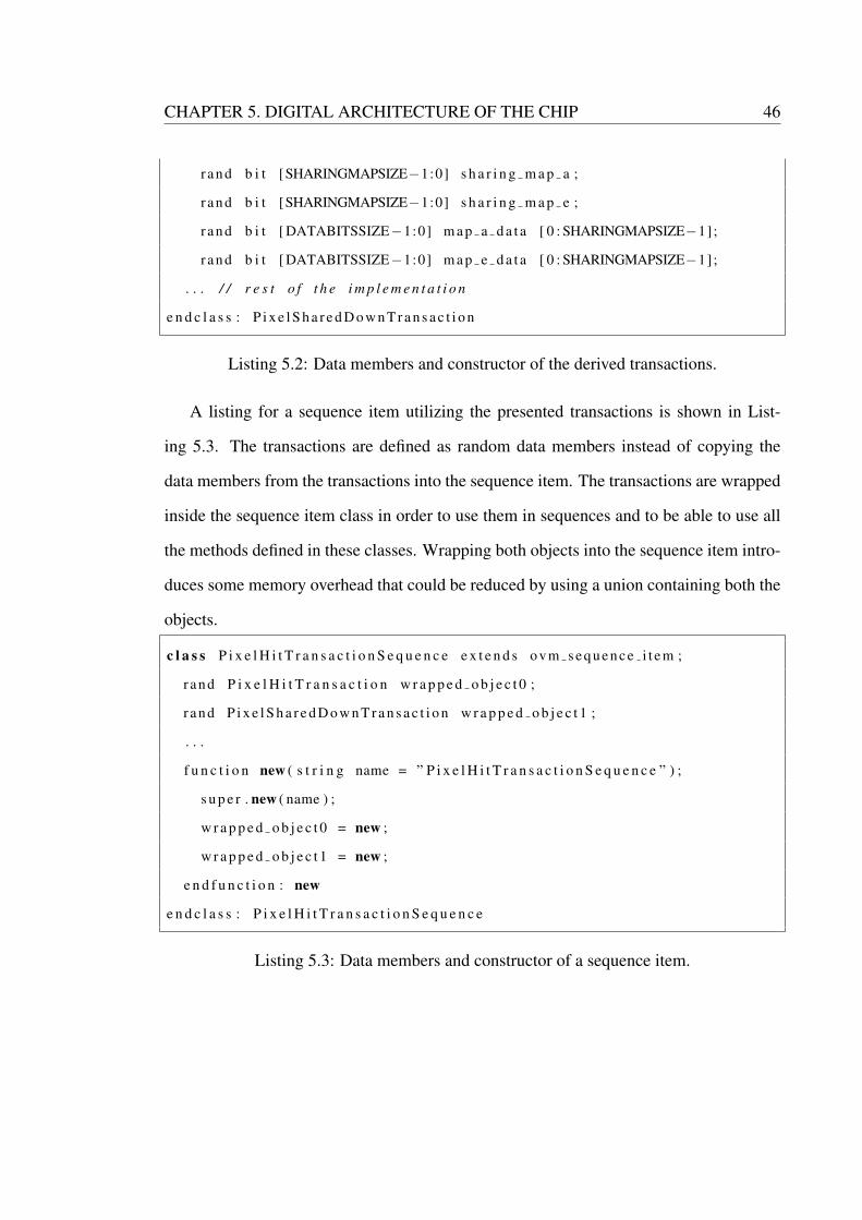
CHAPTER 5. DIGITAL ARCHITECTURE OF THE CHIP 46
r and b i t [SHARINGMAPSIZE−1:0] s h a r i n g m a p a ;
r and b i t [SHARINGMAPSIZE−1:0] s h a r i n g m a p e ;
r and b i t [ DATABITSSIZE−1:0] m a p a d a t a [ 0 : SHARINGMAPSIZE−1];
r and b i t [ DATABITSSIZE−1:0] m a p e d a t a [ 0 : SHARINGMAPSIZE−1];
. . . / / r e s t o f t h e i m p l e m e n t a t i o n
e n d c l a s s : P i x e l S h a r e d D o w n T r a n s a c t i o n
Listing 5.2: Data members and constructor of the derived transactions.
A listing for a sequence item utilizing the presented transactions is shown in List-
ing 5.3. The transactions are defined as random data members instead of copying the
data members from the transactions into the sequence item. The transactions are wrapped
inside the sequence item class in order to use them in sequences and to be able to use all
the methods defined in these classes. Wrapping both objects into the sequence item intro-
duces some memory overhead that could be reduced by using a union containing both the
objects.
c l a s s P i x e l H i t T r a n s a c t i o n S e q u e n c e e x t e n d s ov m s eq ue nc e i t e m ;
r and P i x e l H i t T r a n s a c t i o n w r a p p e d o b j e c t 0 ;
r and P i x e l S h a r e d D o w n T r a n s a c t i o n w r a p p e d o b j e c t 1 ;
. . .
f u n c t i o n new ( s t r i n g name = ” P i x e l H i t T r a n s a c t i o n S e q u e n c e ” ) ;
s u p e r . new ( name ) ;
w r a p p e d o b j e c t 0 = new ;
w r a p p e d o b j e c t 1 = new ;
e n d f u n c t i o n : new
e n d c l a s s : P i x e l H i t T r a n s a c t i o n S e q u e n c e
Listing 5.3: Data members and constructor of a sequence item.
CHAPTER 5. DIGITAL ARCHITECTURE OF THE CHIP 47
5.3 System Component Classes
The system was modeled at a transaction level before starting the RTL development, and
all components use the OVM library and were written in SV. The model provides a simu-
lation and verification framework for the RTL implementation in addition to allowing the
early estimation of performance versus specifications. The data compression efficiency
of clustering schemes, depths of FIFO buffers, latencies of buses and latency of on-chip
zero suppression were all estimated first from the TLM, and then refined into an RTL
implementation.
5.3.1 Super Pixel Group
The block diagram of a super pixel group is illustrated in Fig. 5.2. The stimulus generator
uses non-blocking put ports to inject cluster packets into super pixels. Each super pixel
has a FIFO which is used to store packets while waiting for get-call from the arbiter FIFO.
When a super pixel receives a packet, it transports a request to the arbiter FIFO using non-
blocking transport. The arbiter extracts the address of the super pixel from the request and
sends a response indicating whether the transport was succesful or not. That address is
then stored into an internal FIFO of the arbiter.
The zero suppression module can request a next packet from the arbiter FIFO via
blocking get port. If the arbiter FIFO is empty, the zero suppression module blocks until
there is at least one address in the FIFO. When the next address is found, the arbiter
grabs a packet from a corresponding super pixel using non-blocking get and forwards
the packet to the zero suppression module. The zero suppression module blocks for a
period of time proportional to the information contained in the packet, and then puts the
processed packet into the output FIFO. Note that the put operation can fail if the FIFO is
full, but the operation cannot block.
The output FIFO transports a request to a column arbiter by making a request via the

CHAPTER 5. DIGITAL ARCHITECTURE OF THE CHIP 48
Figure 5.2: Block diagram of super pixel group.
non-blocking port after it has received a packet from the zero suppression. This request
contains the address of super pixel group, and is stored into an address FIFO of the column
arbiter. The column arbiter can use this address to get the next packet from the correct
output FIFO. The port connections between the output FIFO and the column arbiter are
demonstrated in Fig. 5.3.
5.3.2 Pixel Column
The block diagram of a super pixel column is illustrated in Fig. 5.3. The main building
blocks for the column are a column bus arbiter and a number of super pixel groups or
super pixels. The functionality of the column bus has been integrated into the arbiter but a
more modular approach would have been to implement these components independently
of each other. The arbitration method of the bus can be chosen by instantiating a specific
arbitration component in the super pixel column. The method is hidden inside the arbiter

CHAPTER 5. DIGITAL ARCHITECTURE OF THE CHIP 49
Figure 5.3: Block diagram of super pixel column.
and is completely transparent to super pixel groups and EoC-blocks.
The arbiter has an unbounded FIFO for storing the addresses of super pixel groups that
have been hit and have made a request. This FIFO does not correspond to any physical
memory in the final implementation, and is only used to determine the logical order of bus
grants. A realistic latency of the bus and arbitration mechanism have also been modeled
in the arbiter.
Besides the super pixel groups and the arbiter, the pixel column does not contain any
other functional components. Connections between the arbiter and the super pixel groups
are created inside the pixel column class, and the class offers two interface ports for other
classes to interact with functional components inside it. EoC-components can access the
column via a blocking get-port and a stimulus generator can inject packets into the column
using a nonblocking put-port.

CHAPTER 5. DIGITAL ARCHITECTURE OF THE CHIP 50
Figure 5.4: Block diagram of part of the periphery (1/8 of the chip).
5.3.3 Periphery Logic
Periphery logic is located at the bottom of the chip and is not a part of the active area (the
area shown in Fig. 4.2). Part of the periphery is shown in the Fig. 5.4 along with eight
super pixel columns. This corresponds to one eighth of the periphery of one chip.
The readout scheme from column to EoC is controlled by EoC-blocks, which means
that if the FIFO in the EoC-block is full, the EoC-block stops the data transfer until there
is space in the FIFO again. In the RTL model this can be enabled with a simple full-flag.
The TLM model of the block is implemented with a threaded component using a blocking
get-port, a bounded FIFO and a blocking put-port. A get-operation blocks until it receives
a packet from the column and also blocks until the packet can be written into the FIFO in
the EoC-block. Another process in the EoC-block first tries to get a packet from the FIFO
and blocks if the FIFO is empty. When the next packet is available, the EoC-block tries
to put the packet into the EoC bus.

CHAPTER 5. DIGITAL ARCHITECTURE OF THE CHIP 51
The EoC bus is modeled with a non-threaded component which uses a bounded FIFO
with a single slot for a packet. If this FIFO is full, a put-operation will block until the slot
is freed and the packet can be written into the slot. The bus latency is modeled by blocking
the get-operation by delaying the operation for an amount of clock cycles proportional to
the length of the packet divided by the width of the bus. If the FIFO in the bus component
is empty, the get-operation also blocks.
The output FIFO is the last communication channel between output links and the rest
of the periphery. The limited output data bandwidth of the chip is modeled by using a
threaded component with an internal bounded FIFO. The component tries to get a packet
from the internal FIFO every clock cycle and write the packet into an analysis port. This
operation will always succeed and the data rate of the operation (bits per packet) is in
agreement with the data rate simulations presented later in this chapter.
5.3.4 Chip and Simulation Environment
The top class of the chip along with the verification components are shown in Fig. 5.5.
A very simple testbench consists of a stimulus generator and a scoreboard in addition
to the chip object. All hits in transactions are already merged together using a clustering
algorithm before transactions are injected into the chip. This means that the algorithm can
be freely changed without changing anything in the chip. As the data traffic in the chip
uses only sizes of the transactions to estimate bus delays and buffer allocation, the only
information chip needs is the size of the transaction. Each transaction class implements
function size() which returns the size of the transaction in bits.
The scoreboard is used to measure the performance of an instantiated chip architec-
ture. The stimulus generator sends information about input transactions and the score-
board compares them to output transactions received from the chip. The scoreboard cal-
culates efficiency of the architecture (transactions received versus total input transactions),
the worst case latency of all transactions, total data rate and distribution of different sizes
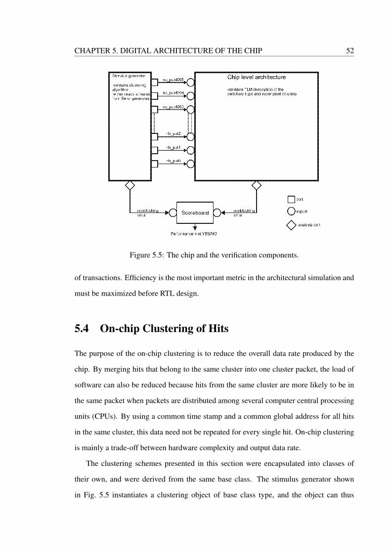
CHAPTER 5. DIGITAL ARCHITECTURE OF THE CHIP 52
Figure 5.5: The chip and the verification components.
of transactions. Efficiency is the most important metric in the architectural simulation and
must be maximized before RTL design.
5.4 On-chip Clustering of Hits
The purpose of the on-chip clustering is to reduce the overall data rate produced by the
chip. By merging hits that belong to the same cluster into one cluster packet, the load of
software can also be reduced because hits from the same cluster are more likely to be in
the same packet when packets are distributed among several computer central processing
units (CPUs). By using a common time stamp and a common global address for all hits
in the same cluster, this data need not be repeated for every single hit. On-chip clustering
is mainly a trade-off between hardware complexity and output data rate.
The clustering schemes presented in this section were encapsulated into classes of
their own, and were derived from the same base class. The stimulus generator shown
in Fig. 5.5 instantiates a clustering object of base class type, and the object can thus
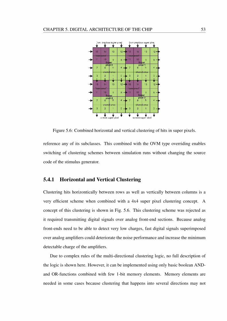
CHAPTER 5. DIGITAL ARCHITECTURE OF THE CHIP 53
Figure 5.6: Combined horizontal and vertical clustering of hits in super pixels.
reference any of its subclasses. This combined with the OVM type overriding enables
switching of clustering schemes between simulation runs without changing the source
code of the stimulus generator.
5.4.1 Horizontal and Vertical Clustering
Clustering hits horizontically between rows as well as vertically between columns is a
very efficient scheme when combined with a 4x4 super pixel clustering concept. A
concept of this clustering is shown in Fig. 5.6. This clustering scheme was rejected as
it required transmitting digital signals over analog front-end sections. Because analog
front-ends need to be able to detect very low charges, fast digital signals superimposed
over analog amplifiers could deteriorate the noise performance and increase the minimum
detectable charge of the amplifiers.
Due to complex rules of the multi-directional clustering logic, no full description of
the logic is shown here. However, it can be implemented using only basic boolean AND-
and OR-functions combined with few 1-bit memory elements. Memory elements are
needed in some cases because clustering that happens into several directions may not

CHAPTER 5. DIGITAL ARCHITECTURE OF THE CHIP 54
always be decided in one clock cycle. For example, if priority is chosen to always do
the clustering down instead of right if possible, super pixel 0 in Fig. 5.6 would first have
to communicate with super pixels 1 and 2 during the first clock cycle, and then send the
results of this communication back to both super pixels during the second clock cycle.
This latency could of course be reduced by connecting super pixels also diagonally but
that would increase the hardware cost even more.
5.4.2 Vertical Clustering
Vertical clustering, shown in Fig. 5.7, is less efficient than the combined horizontal and
vertical clustering, producing over 7 packets per bunch crossing when simulated with a
hit distribution described in the Appendix A. However, it requires less hardware and is
functionally simpler to implement and verify than horizontal clustering while requiring
no inter-column communication on-chip. The vertical clustering was chosen to be imple-
mented also in the RTL design of the super pixels.
Vertical clustering can be decided in one clock cycle, and as soon as the discriminator
outputs are asserted. This means that no additional memory elements are required to
store intermediate results about the clustering, and decision about assigning hits to a single
super pixel can be made before any information is written into the buffer of the super pixel.
Also the combinatorial logic required to implement the vertical clustering, summarized
into Tab. 5.1, is much simpler than in combined horizontal and vertical clustering. The
hyphens in the Tab. 5.1 indicate don’t care -conditions.
5.4.3 Data Rate Comparisons
Table 5.2 shows the output data rates for the chip with the highest hit frequency. The
chip with the highest hit frequency is located in the middle of the module as described in
Chap. 4. It can seen that by using a row header with a variable length hitmap and vertical
clustering, the overall data rate is reduced to 70% of the simpler implementation where

CHAPTER 5. DIGITAL ARCHITECTURE OF THE CHIP 55
Figure 5.7: Vertical clustering of hits between super pixels.
no data fields are shared and each hit is represented by a 16-bit address. The reason for
rejecting combined vertical and horizontal clustering was its expensive hardware cost as
no large gain in data reduction was achieved compared to vertical clustering.
Vertical clustering, which was chosen for the final RTL implementation, can be turned
off by setting a configuration register bit specified in Chap. 4. In fact, a part of the super
pixels in the chip can be programmed to use the clustering logic while the logic can be
turned off in the rest of the super pixels. However, RTL simulations showed that by
turning off the logic in all super pixels, performance requirements for overall efficiency
were not met.

CHAPTER 5. DIGITAL ARCHITECTURE OF THE CHIP 56
Table 5.1: Logic conditions for vertical clustering of hits.
Super pixel 1 Super pixel 0
Pixels 15 – 8 Pixels 7 – 0 Pixels 15 – 8 Pixels 7 – 0 Clustering enabled
YES - - - NO
- - NO - NO
- YES YES - YES
Table 5.2: Data rate comparisons of different encoding and clustering schemes.
Address encoding Clustering type Data rate
No encoding (16-bit address for each hit) No 19.5 Gbps
Fixed 16-bit map No 16.7 Gbps
4-bit row header, variable length map No 14.6 Gbps
4-bit row header, variable length map Vertical 13.55 Gbps
4-bit row header, variable length map Vertical and horizontal 13.27 Gbps

Chapter 6
Register Transfer-Level Design of Super
Pixel
An overview of a super pixel group and its required functionality was given in Chap. 4.
In this chapter the design of digital RTL blocks for the super pixel front-end and common
logic blocks for several super pixels are described.
6.1 Super Pixel Digital Front-end
A block diagram of the digital front-end of the super pixel is presented in Fig. 6.1. Digital
front-end of super pixel performs the following tasks:
• Synchronizes the analog front-end signals with digital logic.
• Encodes headers for cluster packets.
• Assigns a bunch id for clusters and handles ToT counting.
• Manages hitmap buffers and cluster information (count in progress/done).
• Handles inter-super pixel communication and data buffering.
• Makes requests to the arbiter FIFO.

CHAPTER 6. REGISTER TRANSFER-LEVEL DESIGN OF SUPER PIXEL 58
Figure 6.1: Block diagram of the super pixel digital front-end.
The synchronizer contains 6 D-flip-flops per discriminator to detect rising and falling
edges of the signals. It also contains logic to mask rising and falling edges occurring
within a single clock cycle. Edge detection gives better control of the input signals than
directly reading the discriminator signal because signals that last more than a maximum
number of ToT counts still produce only one rising edge.
When at least one rising edge is detected, a write-signal is generated and 16-bit map
of the pixels is written into the hitmap buffer. This write does not happen if the buffer is
already full. In this case, an overflow-signal (not shown in Fig. 6.1) is asserted for one
clock cycle. No information about the cluster is saved into the super pixel and it is up to
the periphery logic to process this overflow. In practice this means that the periphery logic
could create an overflow packet indicating the value of the bunch id when the overflow
happened. Because overflow is implemented as fast-OR of all super pixels in a column,
the periphery logic can only register a bunch id and a column address of the overflown
cluster but not its shape or exact pixel address. A bunch id is also assigned for a map
CHAPTER 6. REGISTER TRANSFER-LEVEL DESIGN OF SUPER PIXEL 59
written into the hitmap buffer to later identify all events that happened at the same clock
cycle.
A copy of the 16-bit map is also written into the ToT register. The original map must
be copied because the ToT register will modifies this map to keep track of the state of
the cluster. The ToT register latches 3 least significant bits (LSBs) of the same counter
that is used for the bunch id on the falling edge of discriminator signals. The register also
has logic to prevent new clusters from overwriting ToT information of old clusters. It can
buffer up two clusters and its internal memory is implemented as a 2 word FIFO. A read-
and write-pointers of this FIFO are protected against SEUs using TMR.
After having registered ToT values for all 1s in a hitmap, the ToT register asserts done-
signal. The signal is asserted until the register receives read-signal from FSM. When
FSM notices done-signal, it makes a request to the arbiter FIFO if cluster was not shared
or writes data into the sharing FIFO otherwise. If data is written into the sharing FIFO,
FSM reads ToT register once and starts to process next cluster if any are available in the
ToT register. If a request is made, FSM has to wait until read-signal from zero suppression
unit through super pixel demux is asserted. After the read-signal arrives, FSM reads the
hitmap buffer and the ToT register, and their read-pointers are incremented.
6.2 Zero Suppression Unit
The zero suppression unit formats cluster packets according to the specifications pre-
sented in Chap. 4. Data needs to be formatted because unformatted data consists of all
the hitmaps and ToT values in a super pixel in addition to the shared information from
communication between super pixels. Each packet payload consists of a number of 4-bit
nibbles that are not ordered before the data formatting. Because ToT values are only 3
bits long, they are padded with an extra zero into the MSB position. The zero suppression
unit has to evaluate the whole payload and shift all the nibbles that contain information

CHAPTER 6. REGISTER TRANSFER-LEVEL DESIGN OF SUPER PIXEL 60
into MSB-positions of a packet. In this way, the final payload can be handled as uniform
bit stream and unnecessary nibbles located at the LSB-positions can be dropped away.
The zero suppression consists of the following parts:
• Format 4-bit row hit patterns using row header.
• Format 4-bit (padded) ToT fields using row hit patterns.
• Format 4-bit row hit patterns indicating shared hits using sharing header.
• Format 4-bit (padded) ToT fields of shared hits using row hit patterns indicating
shared hits.
The block diagram of the zero suppression unit is shown in Fig. 6.2. Some smaller
blocks and connections are omitted for clarity. The state machine has an enable-signal
(not shown) which controls all synchronous blocks. The signal is used to disable the
whole unit when almost full- or full-signal is asserted. In this case, the state machine
keeps its state and no feedback registers or the accumulator is activated. The word shifter
is a purely combinatorial block and is not controlled by the enable-signal. The state
machine is protected against SEU by using triplicated state registers, majority voting and
state refreshing presented in Chap. 2.
The sum out is equal to the number of 1s contained in both the headers. The unit
asserts a write-signal when sum out is >= 4. This indicates that the unit has enough 4-bit
nibbles in output 1 to write them into a dataFIFO which has a word size of 16 bits. The
last write operation is done, when the state machine announces a final state and also the
header information is written into a header FIFO. The accumulator registers the sum of
all 1s contained in all headers during one zero suppression process. This sum is shifted
to right by 2 bits, and then written into the header FIFO. The shift is done because 1 in a
header corresponds to 4 bits but the data FIFO has a word size of 16 bits.
Muxes A and C are used to choose the first word or feedback word depending on the
state of the zero suppression unit. If the two words processed by the shifter do not contain

CHAPTER 6. REGISTER TRANSFER-LEVEL DESIGN OF SUPER PIXEL 61
Figure 6.2: Block diagram of zero suppression unit.
enough 4-bit nibbles, mux B is used to feed the output 1 back to the shifter. Otherwise,
the output 1 is written into the data FIFO as mentioned. Output 0 is then fed back to the
shifter and the next word from the data and header muxes is chosen.
6.3 FIFO buffers
There are two FIFOs in the final stage of the super pixel group before the column bus.
The FIFOs work totally independent of each other but have several identical characteris-
tics. Both FIFOs have synchronous read- and write-operations. Their states are stored in
separate binary encoded read- and write-pointers which are protected against SEUs with
TMR. An extra bit for each pointer is needed to calculate full- and empty-conditions.
They are also both protected against underflow and overflow which means that reading
an empty FIFO or writing to a full FIFO does not override any stored data and does not
corrupt the pointers.
The data FIFO is used to store hitmaps, ToT data, shared hitmaps and shared ToT

CHAPTER 6. REGISTER TRANSFER-LEVEL DESIGN OF SUPER PIXEL 62
data. Data is written 16 bits at time and read 16 bits at time. It does not contain any error
correction or detection for data.
The header FIFO is used to store headers of packets and information about the size
of the payload that was stored into the data FIFO. Using the size information, the state
machine implemented for bus communication knows the length of the bus operations.
Data is written 21 bits at time and and read out 21 bits at time. By storing the address of
the super pixel group into a separate address register, it never needs to be stored into the
header FIFO.
6.4 Bus Logic and Protocol
A slightly modified version of decentralized rotating arbiter with independent requests
and grants [32] is used in the bus protocol. The arbitration scheme used is shown in
Fig. 6.3. A token is initialized into the first (lowest address) arbiter in the column and
circulates until it finds an arbiter with a request. This arbiter keeps the token until bus
busy -signal is deasserted, then asserts the signal again and releases the token. The token
need not be kept in the same arbiter during a bus transaction if starting a transaction is not
allowed without the token. The advantage of releasing the token early is that it is more
likely to find a new arbiter with a request before the bus becomes idle. This increases the
bandwidth of the bus.
Super pixel groups are bus masters and EoC-logic is a bus receiver (not shown in
Fig. 6.3. Bus busy -signal is also used to indicate that data on the bus is valid and should
be read by EoC-logic. An almost done -signal is used to indicate the end of the transaction
and an end of one data packet. During the last bus transaction cycle both the signals are
high and the next arbiter knows that it will get the bus to itself in the next clock cycle. In
this way the bus will be constantly utilized and there are no useless one clock cycle delays
between transactions. This minimum latency data transfer is of course only guaranteed if

CHAPTER 6. REGISTER TRANSFER-LEVEL DESIGN OF SUPER PIXEL 63
Figure 6.3: Rotating token based arbitration and bus lines[32].
the token manages to find next arbiter having data before current transaction ends.
An almost full -signal takes a priority over other functionality on the bus. EoC-logic
can assert the signal any time, and it will block the current transaction which will proceed
only when almost full -signal is deasserted by EoC-logic. This makes the readout scheme
EoC-driven and prevents data overflows in the periphery blocks. This means that each
data packet succesfully received by an EoC-logic will eventually find its way out of the
chip in fewer clock cycles than the maximum range of the bunch counter which was
specified in Chap. 4. By preventing overflows in EoC-logic and periphery it is ensured
that no bandwidth is wasted sending packets down the column and then overflowing them
in the periphery.

Chapter 7
Functional Verification
Functional verification is done using Modelsim and OVM. Architectural optimization and
verification is done by using the TLM description of the architecture of the chip. After
that the functionality and performance of the RTL description of the super pixel is verified
reusing parts of TLM description and developing any OVM verification components that
are required.
Because OVM is based on coverage driven and constrained random verification flow,
coverage collectors, checking scoreboards and random stimulus generator also need to be
embedded into the verification environment and tests. The RTL description of DUT is
treated as a black box in these tests which means that no internal information about the
DUT is available to verification components. This makes it easier to reuse the components
in system level and chip level verification tests.
7.1 Analog Pixel Agent
An agent that is used to model the discriminator signals from the analog front-end is
shown in Fig. 7.1. The agent is constructed using guidelines mentioned in [24, 2] to max-
imize the reuse and configurability of the verification component. This means that the
agent needs to be able to operate on its own without external stimulus and also provide

CHAPTER 7. FUNCTIONAL VERIFICATION 65
Figure 7.1: Block diagram of OVM-based component analog pixel agent.
scoreboards and other subscriber components with analysis information via an analysis
port. The agent is used as a wrapper to contain all necessary information about the inter-
face protocol for driving the DUT.
As many pixel chips [4, 30, 5] are designed with similar analog-to-digital interfaces,
using either one or two discriminator signals per pixel, the agent should be highly config-
urable using the mechanism built into OVM.
The main task of the agent is to keep the discriminator signals high for a number
of clock cycles indicated by sequence items created by the analog pixel sequencer. The
monitor in the agent is used to record these input transactions and send them to subscriber
components such as scoreboards and coverage collectors. The monitor is also independent
of other components in the agent meaning that the agent can be instantiated containing
only the monitor. This is particularly useful when the DUT needs to be verified in a
mixed-signal simulation where drivers are replaced, for example, with a Verilog-AMS
description of the analog front-end.
The analog pixel agent can also be instantiated with different configurations of drivers.
The transaction driver can accept transactions from external random generator and drive

CHAPTER 7. FUNCTIONAL VERIFICATION 66
them into the DUT similarly to the driver that pulls its stimulus from the sequencer. Using
the transaction driver instead of the analog pixel driver does not have any impact on the
operation of the monitor.
All drivers and the monitor can be configured to support any number of discriminator
signals. This means that the agent can be used at a block level to verify small blocks with
as little as one discriminator signal, and at the chip level verifying a full chip of 256 x 256
discriminator signals. The coverage collector has options for collecting coverage from
4, 64 or 4096 super pixels but the default coverage collector can be overridden using the
factory-mechanism of OVM if desired.
Finally, the transaction master can also be used with an external stimulus generator
and it can be used to drive TLM transactions into an architectural TLM description of
the system. In this case the monitor cannot be used but coverage can be collected and
transactions can be sent to a scoreboard using the analysis port in the transaction master.
The analog pixel driver, the transaction driver and the transaction master are mutually
exclusive.
When instantiated with the sequencer and the driver, the agent also needs a sequence
library. The sequence library works as an API for a test writer and new sequences can
also be added to the library or constructed in a hierarchical manner out of already existing
sequences in the library. In practice each sequence is created using the sequence item
presented in Chap. 5 and can be used to create a pattern of 4 x 4 pixels and corresponding
ToT value for each single hit contained in the pattern. Each sequence can also be directed
into certain address by constraining the randomized address values. The driver is respon-
sible for the protocol between the agent and DUT, which means that sequences do not
have to contain any timing or protocol specific information. The talker component is use-
ful in debugging by printing out the information about each transaction that the monitor
samples from the bit-level signals between the agent and DUT.

CHAPTER 7. FUNCTIONAL VERIFICATION 67
Figure 7.2: Block diagram of OVM-based component group logic agent.
7.2 Group Logic Agent
It was mentioned in Chap. 5 that a hardware algorithm for merging clusters between
super pixels was implemented. The group logic agent, shown in Fig. 7.2, is used to model
and verify the functionality of clustering logic between super pixels. The agent has two
mutually exclusive driver configurations for modeling a next super pixel group and a
previous super pixel group in a column (see Chap. 5 for the description of the column).
The same sequencer can be used for both driver configurations and the monitor does
not need to be changed. The sequence library of the analog pixel agent is reused in
the group logic agent because the sequence items created in both sequencers in different
agents are similar.
7.3 Column Bus Agent
A verification component that is used to model and monitor the functionality of the col-
umn bus is shown in Fig. 7.3. This component is designed to be used when verifying
at super pixel block level and at column level. One bus agent is needed for each col-
umn because the agent needs to act as an active bus transactor modeling the behaviour of
EoC-block.

CHAPTER 7. FUNCTIONAL VERIFICATION 68
Figure 7.3: Block diagram of OVM-based component column bus agent.
The column bus agent has three different drivers that are designed to be used at dif-
ferent levels of verification. Because the data flow in the bus is in only one direction
as presented in the previous chapter, no sequencers are designed to be used with these
drivers. All drivers have to implement the column bus protocol described in the previous
chapter.
The single bus driver is designed to be used at a block level when verifying a super
pixel group. This driver functions as an EoC receiver as well as models the behaviour
of other super pixel groups on the bus. This means that the driver can grab a bus to
itself when a DUT releases the bus token and keep it for a certain amount of time. The
driver is also able to stop the data flow of the bus by asserting an almost full-signal. By
implementing both of these functionalities it is ensured that all features of DUT related to
the bus protocol are verified.

CHAPTER 7. FUNCTIONAL VERIFICATION 69
Figure 7.4: Complete OVM-based testbench for super pixel group RTL-module.
7.4 Complete Testbench for Super Pixel Group
The complete testbench for the super pixel group is shown in Fig. 7.4. There are four
different agents, a pixel transaction merger and a scoreboard. The agents were already
described in the previous sections of this chapter.
The merger is used to implement the on-chip clustering function to decouple this
algorithm from the agent. Because the agent does not know the algorithm, it is easier
to use the agent in verifying blocks without the algorithm or to replace the algorithm by
instantiating a merger of another type. The merger is not completely transparent to the
scoreboard and adds some latency to forwarding the transactions to scoreboard. Latency is
needed because the monitor in the analog pixel agent may finish sampling two transactions

CHAPTER 7. FUNCTIONAL VERIFICATION 70
Table 7.1: Different errors in transactions and their severity.
Error Flag Critical
Bunch ID Yes
Row Header Yes
Super Pixel Address Yes
Group Address Yes
Hitmap Yes
Sharing Header No
Shared Hitmap Only if Sharing Header error
ToT Value No
Shared ToT Value No
Payload Length No
that belong to the same bunch crossing at different time.
By buffering transactions for a certain amount of time the merger ensures that it re-
ceives all transactions from single bunch crossing before applying the clustering algo-
rithm. The latency must be carefully chosen because the merger must forward transac-
tions to the scoreboard before the column bus agent receives a corresponding transaction
from the DUT and sends it to the scoreboard. Otherwise a missing transaction will be
reported by the scoreboard.
The scoreboard has several FIFOs to receive transactions from different agents. It
blocks until there is a transaction received from the column bus agent. This transaction
corresponds to the output of the DUT and is compared to the transaction data collected
from other agents. A compare-function is implemented inside the transaction class and
it will produce an error code that corresponds to the mismatch in compared transactions.
These codes are used only to determine errors in verification and are not implemented
anywhere in the DUT. Different error possibilities are listed in Tab. 7.1.

CHAPTER 7. FUNCTIONAL VERIFICATION 71
A critical error in the Tab. 7.1 indicates presence of a design error. The source of the
error must be traced, and logic corrected to remove this error from the design. All of the
errors, including non-critical ones, can also happen due to wrong or missing connections
in RTL code. They can be caused by FIFO pointers that are not incremented correctly
or do not wrap around correctly. This needs to be always observed because the final size
of the FIFO is not always a power of two, and thus binary-encoded pointers may not be
using all possible values in their dynamic range.
Non-critical errors are always assumed to result from the pre-buffer overflow in the
super pixel front-end. They are not functional errors, but errors in the data due to per-
formance limitations of the front-end. When a non-critical error is a result of a missing
or wrong connection in RTL code or FIFO pointer error, it is actually a critical error and
must be debugged. When this happens there are of course errors in other data fields (FIFO
pointer case) or the error is systematic (connections error) so these critical errors can be
distinguished from non-critical ones by observing the output packets when an error is
reported.
7.5 Complete Testbench For Super Pixel Column
A complete testbench for functional and performance verification of the super pixel col-
umn is shown in Fig. 7.5. The testbench consists of the same agents as the group-level
environment but two agents modeling group logic between groups have been removed.
Also instead of using the driver-sequencer pair in analog pixel agent, an external stimulus
generator is used to inject transactions into the analog pixel agent. The agent is configured
to use the transaction driver which is not coupled with a sequencer.
The generator works completely asynchronously of the DUT, and either generates
randomized transactions or reads them from an external file. External files can contain
results, for example, from physics simulations or event generators. This enables the ver-

CHAPTER 7. FUNCTIONAL VERIFICATION 72
Figure 7.5: Complete OVM-based testbench for super pixel column RTL-module.
ification of architectural and RTL performance for various number of experiments and
systems merely by supplying the external stimulus file for the testbench. Because the
generator is asynchronous to the DUT, the transaction driver in the analog agent handles
all the synchronization between stimulus and the DUT.
Chapter 8
Simulation and Synthesis Results
8.1 Simulations
The simulations were done using Mentor Graphics’ Modelsim and the results presented
here were obtained from the RTL and the TLM simulations. The data sets used were
taken from Gauss/Boole simulations performed at CERN. Characteristics of the data sets
are described in Appendix A, and the used stimuli were from the chip H and chip G of
the module of 10 chips (see Fig. 4.1 in Chap. 4).
8.1.1 Latency
Latency of packets in the chip H (shown in Fig. 4.1) is shown in Fig. 8.1. Notice that the
y-axis is printed on a logarithmic scale. The architectural simulations at a transaction level
showed that the maximum latency for transporting a packet out of the chip was within a
dynamic range of 12 bits (4096 clock cycles). This dynamic range was verified with the
RTL simulations to be sufficient. It can be seen from Fig. 8.1 that the latency of packets
from the digital front-end to EoC is approximately 600 clock cycles. This gives over 3000
clock cycles (clocking at 40 MHz) to transport the packets from EoC buffers to the output
links of the chip. Because the full chip was not modeled at RTL in this thesis, this number

CHAPTER 8. SIMULATION AND SYNTHESIS RESULTS 74
Figure 8.1: Latency of packets from digital front-end to end of column.
is given as a specification for the further development of the periphery of the chip.
8.1.2 Length of Data Packets
Figure 8.2 shows the distribution of packets of different lengths in chips G and H (spec-
ified in Fig. 4.1). This information is essential in defining the size of the EoC buffer
of the next stage as well as ’almost full’ threshold for the buffer in order to guarantee
uninterrupted bus transactions as often as possible. Because interruption of a bus trans-
action will cause the bus to be idle for at least one clock cycle, minimizing the number
of interruptions by choosing a right threshold value will improve the performance of the
bus.
By observing Fig. 8.2, it can be seen that the performance of address encoding algo-
rithm using row header is different in chips G and H . In the chip G , there are three

CHAPTER 8. SIMULATION AND SYNTHESIS RESULTS 75
Figure 8.2: Distribution of different packet sizes in chips G and H .

CHAPTER 8. SIMULATION AND SYNTHESIS RESULTS 76
times the amount packets of 42 bits while in the chip H there are three times the amount
of packets of 46 bits as there are in the chip G . Typically a 42-bit packet is produced
when there is a 2-pixel horizontal cluster in a packet while a 46-bit packet is produced by
any other type of cluster of 2 pixels. The impact of row header address encoding on over-
all data rate reduction over simpler address encoding methods was already presented in
Tab. 5.2. However, it should be noted that the efficiency of the algorithm depends heavily
on sizes and shapes of clusters.
8.1.3 Efficiency and Data Rates
Efficiencies and data rates across columns of the chips G and H are shown in Fig. 8.3.
For the chip H , the efficiency is over 99% in all columns. However, there is a difference
of approximately 0.2% in efficiencies of columns 28 and 34 although the data rates are
almost identical. The column 28 has 4 super pixels with a hit frequency over 200 kHz
while the column 34 only has 3 of them. This might be a partial reason for lower efficiency
in the other column but also the timing of the hits can have an impact on the overall
efficiency.
Table 8.1 shows the efficiency in RTL simulations with different FIFO sizes. These
results were obtained using a super pixel column 28 which was found to be the column
generating more data than any other column in chip H . The FIFO was previously shown
to be included in the final block of super pixel group in Fig. 4.4. Total size of the super
pixel group is also shown in Tab. 8.1. It can be seen from Tab. 8.1 that in general the
overall efficiency improves when the size of the FIFO is increased if right combination
of words for the header FIFO and the data FIFO are chosen, and Fig. 8.4 also shows this
trend.
However, just by increasing the absolute area of the FIFO alone does not result in
increased readout efficiency. Another important parameter besides the absolute area of
the FIFO is the right size combination of words in the data FIFO and the header FIFO.

CHAPTER 8. SIMULATION AND SYNTHESIS RESULTS 77
Figure 8.3: Efficiencies and data rates in chips G and H .
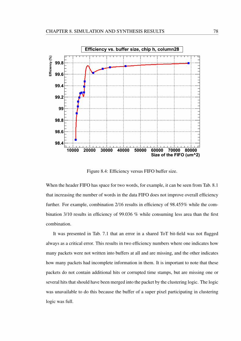
CHAPTER 8. SIMULATION AND SYNTHESIS RESULTS 78
Figure 8.4: Efficiency versus FIFO buffer size.
When the header FIFO has space for two words, for example, it can be seen from Tab. 8.1
that increasing the number of words in the data FIFO does not improve overall efficiency
further. For example, combination 2/16 results in efficiency of 98.455% while the com-
bination 3/10 results in efficiency of 99.036 % while consuming less area than the first
combination.
It was presented in Tab. 7.1 that an error in a shared ToT bit-field was not flagged
always as a critical error. This results in two efficiency numbers where one indicates how
many packets were not written into buffers at all and are missing, and the other indicates
how many packets had incomplete information in them. It is important to note that these
packets do not contain additional hits or corrupted time stamps, but are missing one or
several hits that should have been merged into the packet by the clustering logic. The logic
was unavailable to do this because the buffer of a super pixel participating in clustering
logic was full.

CHAPTER 8. SIMULATION AND SYNTHESIS RESULTS 79
Table 8.1: Efficiency, average data rate and buffer size in a super pixel group.Efficiency Efficiency FIFO size, Proportional Total area
(%, missing packets) (%, correct packets) num. of words, and absolute of group
header/data area of FIFO
98.940 98.455 2/10 10.5 %, 11658 µm2 110386 µm2
98.940 98.455 2/12 11.6 %, 13043 µm2 112220 µm2
98.940 98.455 2/16 13.3 %, 15656 µm2 114833 µm2
99.150 98.916 3/9 11.1 %, 12313 µm2 111491 µm2
99.240 99.036 3/10 11.5 %, 12975 µm2 113153 µm2
99.246 99.060 3/16 14.6 %, 16937 µm2 116150 µm2
89.816 88.906 4/8 not synthesized not synthesized
99.264 99.120 4/9 11.7 %, 13169 µm2 112345 µm2
99.341 99.192 4/10 12.3 %, 13821 µm2 113007 µm2
99.395 99.264 4/11 12.8 %, 14498 µm2 113674 µm2
99.407 99.276 4/12 13.3 %, 15216 µm2 114392 µm2
99.413 99.282 4/14 14.4 %, 15216 µm2 115834 µm2
99.401 99.240 5/10 13.5 %, 15442 µm2 114818 µm2
99.497 99.383 5/12 14.5 %, 16827 µm2 116003 µm2
99.563 99.473 6/12 15.2 %, 17010 µm2 116886 µm2
99.677 99.623 8/16 18.2 %, 22099 µm2 121275 µm2
99.731 99.685 10/20 21.8 %, 27701 µm2 126877 µm2
99.749 99.719 12/24 24.4 %, 32049 µm2 131224 µm2
99.77 99.74 16/32 29.4 %, 41209 µm2 140388 µm2
99.82 99.79 32/64 44.2 %, 78428 µm2 177696 µm2
CHAPTER 8. SIMULATION AND SYNTHESIS RESULTS 80
8.2 RTL Synthesis and Place and Route
8.2.1 RTL Synthesis
RTL synthesis was carried out using Cadence’s RTL Compiler. Manual clock gating of
modules was embedded in RTL code before the synthesis but an automated clock gating
was also used in synthesis. This led to significant area reduction as most of the flip-flops
with a feedback mux were replaced with muxless versions. The clock gating also reduced
the dynamic power consumption to 85% of the original value. This result was obtained
after RTL synthesis.
All synthesizable RTL code was written in SV. One of the most useful features which
SV added to the Verilog standard was the ability to use multi-dimensional arrays as mod-
ule ports. All multi-dimensional arrays were properly handled by the synthesis tool, and
functional verification ensured that post-synthesis netlist was correct. SV keywords al-
ways ff and always comb were used to convey designer’s intent to the synthesis tool to
produce a warning if a latch was inferred instead of flip-flop, for instance. SV interfaces
or modports were not used in RTL code.
8.2.2 Place and Route
Place and route of the super pixel group was done using Cadence’s SoC Encounter. The
layout of the super pixel group after place and route is shown in Fig. 8.5. The automated
place and route was done with SoC Encounter after a Verilog netlist was obtained from
RTL synthesis with RTL Compiler. The height of the layout is 870 µm and the width is
165 µm. Configuration registers are placed on both sides of the layout but are shown only
on the left side in Fig. 8.5.
A full column of 16 super pixel groups was placed and routed, and the clock tree
synthesis was also performed. This resulted in a column measuring 165 µm x 1.4080 cm
including buffering for the clock tree and all global signals. A full column consumes ap-

CHAPTER 8. SIMULATION AND SYNTHESIS RESULTS 81
Figure 8.5: Overview of the placement of different modules in the layout of the super
pixel group.

CHAPTER 8. SIMULATION AND SYNTHESIS RESULTS 82
proximately 16 mW in a normal operation mode with a supply voltage of 1.2 volts. Most
of this power, approximately 14 mW, was consumed by the clock tree running at 40 MHz
and having a skew of less than 600 ps. For low-power design, the skew requirements could
have been relaxed, and two different clock trees used for local communication and global
communication. The full column was simulated and verified using the same testbench
used in RTL simulation and functional verification.

Chapter 9
Conclusions And Future Work
The feasibility to design and implement a front-end ASIC for VELO detector of Large
Hadron Collider beauty (LHCb) experiment at CERN in 130nm CMOS technology, and
especially its digital readout architecture was studied in this thesis. The contribution of the
author is the implementation and testing of several architectures at the transaction level.
Based on the transaction level modelling and simulation, the author participated actively
the design and development of the digital readout chip at regular chip design meetings
of VELO at CERN. During these meetings various ideas and a couple of architectures
were considered. In addition to transaction level modelling, the author designed the func-
tional verification environment and implemented the RTL modules of the chip as well as
simulated and synthesised it.
At the transaction level, architectures of the chip were simulated with generated ran-
dom hit patterns and data sets from physics simulations performed by other members
of VELO group. Raising abstraction level in the architectural modeling from RTL to TL
was done to reduce the simulation and debugging time, and to keep the architecture highly
configurable before the final specifications were decided. TLM ports offered much greater
flexibility in this case than bit-level interfaces typically used at RTL. However, even in
TLM in massively parallel simulations of thousands of processing elements (super pixels
in this case), one needs to make sure that most of the elements are non-threaded, reactive
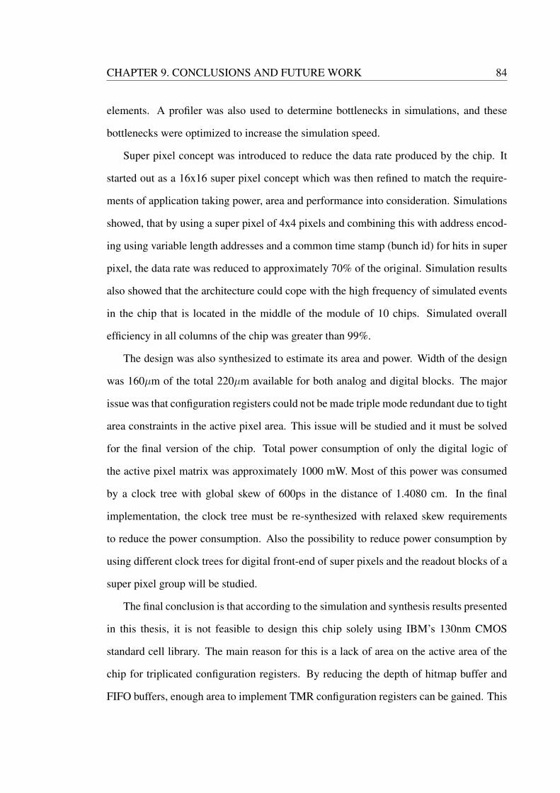
CHAPTER 9. CONCLUSIONS AND FUTURE WORK 84
elements. A profiler was also used to determine bottlenecks in simulations, and these
bottlenecks were optimized to increase the simulation speed.
Super pixel concept was introduced to reduce the data rate produced by the chip. It
started out as a 16x16 super pixel concept which was then refined to match the require-
ments of application taking power, area and performance into consideration. Simulations
showed, that by using a super pixel of 4x4 pixels and combining this with address encod-
ing using variable length addresses and a common time stamp (bunch id) for hits in super
pixel, the data rate was reduced to approximately 70% of the original. Simulation results
also showed that the architecture could cope with the high frequency of simulated events
in the chip that is located in the middle of the module of 10 chips. Simulated overall
efficiency in all columns of the chip was greater than 99%.
The design was also synthesized to estimate its area and power. Width of the design
was 160µm of the total 220µm available for both analog and digital blocks. The major
issue was that configuration registers could not be made triple mode redundant due to tight
area constraints in the active pixel area. This issue will be studied and it must be solved
for the final version of the chip. Total power consumption of only the digital logic of
the active pixel matrix was approximately 1000 mW. Most of this power was consumed
by a clock tree with global skew of 600ps in the distance of 1.4080 cm. In the final
implementation, the clock tree must be re-synthesized with relaxed skew requirements
to reduce the power consumption. Also the possibility to reduce power consumption by
using different clock trees for digital front-end of super pixels and the readout blocks of a
super pixel group will be studied.
The final conclusion is that according to the simulation and synthesis results presented
in this thesis, it is not feasible to design this chip solely using IBM’s 130nm CMOS
standard cell library. The main reason for this is a lack of area on the active area of the
chip for triplicated configuration registers. By reducing the depth of hitmap buffer and
FIFO buffers, enough area to implement TMR configuration registers can be gained. This

CHAPTER 9. CONCLUSIONS AND FUTURE WORK 85
comes at expense of performance that will drop below 99% as shown in the previous
chapter.
This can be solved by using full-custom cells and blocks in some parts of the active
area, the performance could be kept same (efficiency >99%) while gaining area to imple-
ment TMR configuration registers. If done this way, full-custom cells and blocks should
be characterized in order to use them as a part of automated place-and-route flow.

References
[1] Gerhard Lutz. Semiconductor Radiation Detectors. Springer Link, 2007.
[2] Mentor Graphics and Cadence. Open Verification Methodology (OVM) user’s
guide. http://www.ovmworld.org. Cited on 3 February 2010.
[3] L. Rossi et al. Pixel detectors - from fundamentals to applications. Springer, Berlin
Heidelberg, 2006.
[4] X. Llopart. Design and characterization of 64K Pixels Chips Working in Single
Photon Processing Mode. PhD thesis, Mid Sweden University, Sundsvall, 2007.
[5] R. Ballabriga, M. Campbell, E.H.M. Heijne, X. Llopart, and L. Tlustos. The
Medipix3 Prototype, a Pixel Readout Chip Working in Single Photon Counting
Mode with Improved Spectrometric Performance. Nuclear Science Symposium Con-
ference Record, IEEE, 6:3557–3561, 2006.
[6] D. Arutinov et al. Digital Architecture and Interface of the New ATLAS Pixel Front-
End IC for Upgraded LHC Luminosity, volume 56. April 2009.
[7] Ch. Hu-Guo et al. CMOS pixel sensor development: a fast read-out architecture
with integrated zero suppression. J. Inst., 4(4):1–10, April 2009.
[8] G.Dellacasa et al. Pixel Read-Out Architectures for the NA62 GigaTracker. 2009.

REFERENCES 87
[9] C. S. Guenzer, E. A. Wolicki, and R.G. Allas. Single Event Upset of Dynamic RAMs
by Neutrons and Protons. IEEE Transactions on Nuclear Science, 26:5048–5053,
December 1979.
[10] J. T.Wallmark and S. M. Marcus. Minimum size and maximum packing density of
non-redundant semiconductor devices. Proc. IRE, 50:286–298, 1962.
[11] Oluwole A. Amusan et al. Charge Collection and Charge Sharing in a 130 nm
CMOS Technology. IEEE Transactions on Nuclear Science, 53:3253–3258, De-
cember 2006.
[12] Alan D. Tipton et al. Multiple-Bit Upset in 130 nm CMOS Technology. IEEE
Transactions on Nuclear Science, 53:3259–3264, 2006.
[13] Carl Carmichael. Triple Module Redundancy Design Techniques for Virtex FPGAs.
Application Note 197, 2006.
[14] F.L. Kastensmidt et al. Fault-tolerance techniques for SRAM-Based FPGAs.
Springer, Dordrecht, 2006.
[15] SystemVerilog Language Reference Manual. http://www.systemverilog.
org. Cited on 3 February 2010.
[16] S. Sutherland, S. Davidmann, and P. Flake. SystemVerilog for Design. Springer,
USA, 2 edition, 2006.
[17] C. Spear. SystemVerilog for Verification. Springer, USA, 2006.
[18] J. Bergeron, E. Cerny, A. Hunter, and A. Nightingale. Verification Methodology
Manual for SystemVerilog. Springer, 2005.
[19] J. Bergeron. Writing Testbenches Using SystemVerilog. Springer, 2006.
[20] S. Prata. C++ Primer Plus. Sams Publishing, USA, 4 edition, November 2001.

REFERENCES 88
[21] Frank Ghenassia et al. Transaction level modeling with SystemC. Springer, Dor-
drecht, 2005.
[22] L. Cai and D. Gajski. Transaction Level Modeling: An Overview. First
IEEE/ACM/IFIP International Conference on Hardware/Software Codesign and
System Synthesis, 1, 2003.
[23] D.C. Black and J.Donovan. SystemC: From the ground up. Springer, New York,
2004.
[24] Mark Glasser. Open Verification Methodology Cookbook. Springer, 2009.
[25] Jonathan Bromley. Seamless Refinement from Transaction Level to RTL Using
SystemVerilog Interfaces. SNUG 2008 Europe, 2008.
[26] Avinash C. Kak. Programming with Objects: A Comparative Presentation of
Object-Oriented Programming with C++ and Java. John Wiley and Sons, 2003.
[27] Iain D. Craig. Object-Oriented Programming Languages: Interpretation. Springer,
2007.
[28] LHC Design Report Volume 1. Technical Report 1, CERN, 2004. Cited on 24
February 2010.
[29] Paula Collins et al. The LHCb VELO Upgrade.
[30] K. Ito, B. Tongprasit, and T. Shibata. A Computational Digital Pixel Sensor Featur-
ing Block-Readout Architecture for On-Chip Image Processing. IEEE Transactions
on Circuits and Systems I: Regular papers, 56:114–123, 2009.
[31] O. Cobanoglu, P.Moreiro, and F.Faccio. A Radiation Tolerant 4.8 Gb/s Serializer
for the Giga-Bit Transceiver. Proceedings of Topical workshop on Electronics for
Particle Physics, September 2009.

REFERENCES 89
[32] Juha Plosila. Multiprocessor Architectures, lecture slides, 2008.

Appendix A
Hit Distributions in Simulations
This appendix describes the stimuli that was used to obtain the simulation results pre-
sented in this thesis. Two data sets from two different chips of the same module were
used to measure and verify the required performance. Chip H , located in the middle
of the module was used to verify the required performance. Chip G was only used to
measure the maximum performance of the architecture, and efficiency was not required
to exceed 99 per cent in these simulation runs.
A.1 Chip H distributions
Figure A.1 shows the nonuniform distribution of hits between different super pixel columns
on the chip H . This chip is located in the middle of the module consisting of 10 chips
which was presented in Chap. 4.
Figure A.2 shows the distribution of hits in the column 28 of the chip H . This column
had the highest data rate of the chip and was used to determine the minimum required
depths for buffers in order to have an efficiency higher than 99%.
Figure A.3 shows the distribution of hits in the column 34 of the chip H . This column
had data rate almost similar to the column 28 but the efficiency was approximately 0.2 %
higher than in the column 28.

APPENDIX A. HIT DISTRIBUTIONS IN SIMULATIONS A-2
Figure A.1: Distribution of hits among super pixel columns in the chip H .

APPENDIX A. HIT DISTRIBUTIONS IN SIMULATIONS A-3
Figure A.2: Frequency of hits in the column 28 of the chip H .
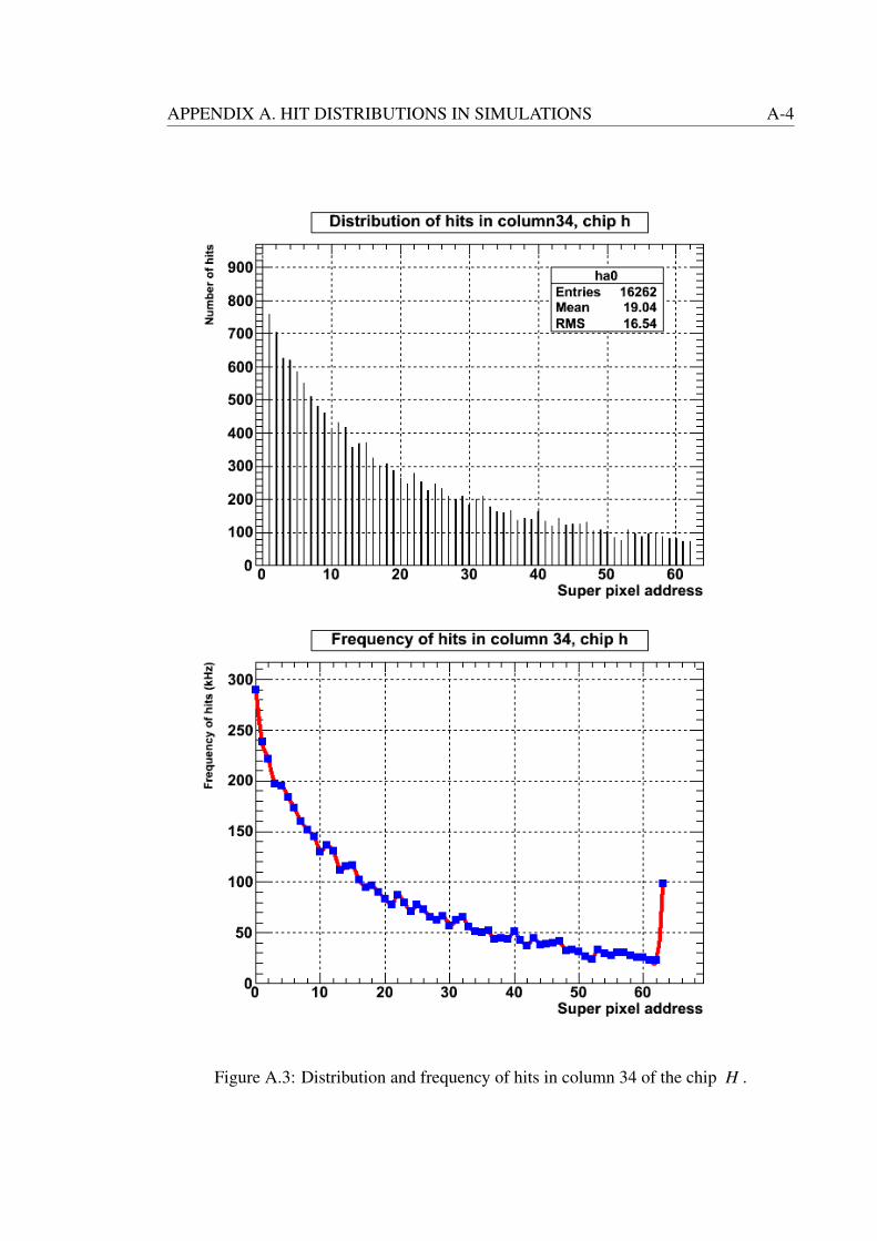
APPENDIX A. HIT DISTRIBUTIONS IN SIMULATIONS A-4
Figure A.3: Distribution and frequency of hits in column 34 of the chip H .

APPENDIX A. HIT DISTRIBUTIONS IN SIMULATIONS A-5
Figure A.4: Distribution of hits among super pixel columns in the chip G .
A.2 Chip G distributions
Figure A.4 shows the nonuniform distribution of hits between different super pixel columns
on the chip G . This chip is located on the left side of the beam in the module consisting
of 10 chips which was presented in Chap. 4.
Figure A.5 shows the distribution of hits in the column 63 of the chip G . This column
had the highest data rate of the chip and was used to determine how the readout architec-
ture could be improved in order to increase the overall efficiency. The column 63 of the
chip G had an efficiency of 86 per cent. Because the layout of the module of 10 chips
will most likely differ from what was presented in Chap. 4, the distributions of hits in
chip G will change.
Figure A.6 shows the distribution of hits in the column 57 of the chip G . This column
is interesting because its efficiency is over 99.2% while the data rate is approaching 290
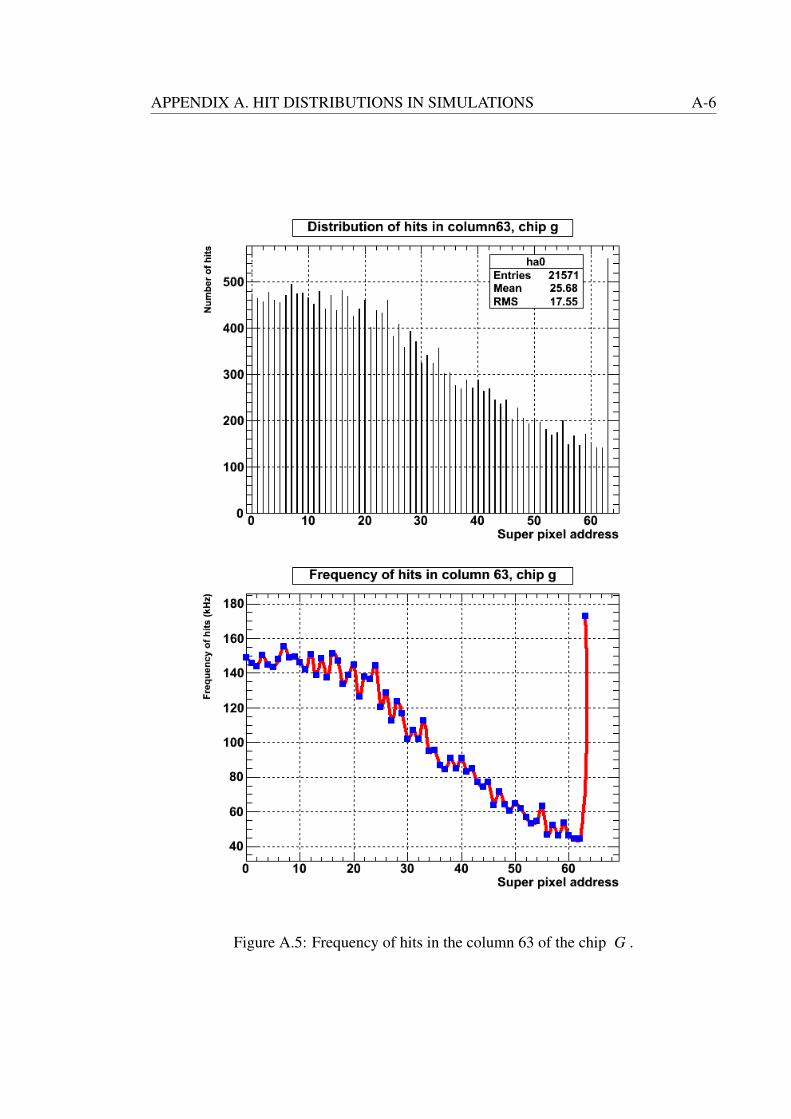
APPENDIX A. HIT DISTRIBUTIONS IN SIMULATIONS A-6
Figure A.5: Frequency of hits in the column 63 of the chip G .

APPENDIX A. HIT DISTRIBUTIONS IN SIMULATIONS A-7
Mbps. When compared to the column 28 of the chip H which had effiency of 99.030%
while having data rate of 241 Mbps, it can be observed by comparing distributions in
Fig. A.2 and Fig. A.6 that more uniform distribution results in better data rates. This of
course implies that larger local hit frequency in a super pixel may have a large impact on
the global efficiency.
APPENDIX A. HIT DISTRIBUTIONS IN SIMULATIONS A-8
Figure A.6: Distribution and frequency of hits in column 57 of the chip G .


![BUILDING PREMIUM BRAND - GMC MEDIA · 2016. 8. 29. · Magazine 65k / month 65K/ month Website 2,500K UV / month Marie Claire TV. ... June 2016 Lifestyles - Beauty/Fashion/Style [Undup.]](https://static.fdocuments.net/doc/165x107/5fee5f046aefa00c442c538c/building-premium-brand-gmc-2016-8-29-magazine-65k-month-65k-month-website.jpg)