Inverting Converter, Switching Regulator - Buck Boost, ON ...

DESIGN AND SIMULATION OF SOFT SWITCHING BOOST
CONVERTER FOR PHOTOVOLTAIC SYSTEM
DEVENDRA KUMAR MISHRA
Department of Electrical Engineering
National Institute Technology, Rourkela-769008
CORE Metadata, citation and similar papers at core.ac.uk
Provided by ethesis@nitr

DESIGN AND SIMULATION OF SOFT SWITCHING BOOST
CONVERTER FOR PHOTOVOLTAIC SYSTEM
A THESIS SUBMITTED IN PARTIAL FULFILMENTS OF THE REQUIREMENTS FOR THE
AWARD OF THE DEGREE OF
Master of Technology
In
Industrial Electronics
By
DEVENDRA KUMAR MISHRA
Roll No: 213EE5346
Under the Guidance of
Dr. MONALISA PATTNAIK
Department of Electrical Engineering
National Institute Technology, Rourkela-769008
May 2015
NATIONAL INSTITUTE OF TECHNOLOGY
ROURKELA
CERTIFICATE
This is to certify that the project entitled “DESIGN AND SIMULATION OF SOFT
SWITCHING BOOST CONVERTER FOR PHOTOVOLTAIC SYSTEM” submitted by
Devendra Kumar Mishra (213ee5346) in partial fulfillment of the requirements for the award
of Master of Technology degree in Industrial Electronics, Department of Electrical
Engineering at National Institute of Technology, Rourkela is an authentic work carried out by
her under my supervision and guidance.
To the best of my knowledge the matter embodied in this thesis has not been
submitted to any other university/Institute for the award of any Degree.
Date:
Place: Rourkela
Dr. Monalisa Pattnaik
Department of Electrical Engineering
National Institute of Technology
Rourkela-769008
Email id: [email protected]

ACKNOWLEDGEMENT
On the submission of my thesis entitled “DESIGN AND SIMULATION OF SOFT
SWITCHING BOOST CONVERTER FOR PHOTOVOLTAIC SYSTEM” I would like
to extend my gratitude and sincere thanks to my supervisor Dr. Monalisa Pattnaik, Asst.
professor, Dept. of Electrical Engineering for her constant motivation and support during the
course work. I am very thankful to her for giving me good basics during the course work.
I would like to thank all others who have consistently encouraged and gave me moral
support, without whose help it would be difficult to finish this project.
I would like to thank my parents and friends for their consistent support throughout.
Date:
Place: Rourkela
Devendra Kumar Mishra
Roll. No. 213EE5346

CONTENTS
ABSTRACT
LIST Of TABLES
LIST OF FIGURES
LIST OF ABBREVIATIONS
LIST OF SYMBOLS
i
ii
iii
iv
v
1.1
1.2
1.3
1.4
1.5
CHAPTER- 1 INTRODUCTION
Overview
1.1.1 Losses in Semiconductor Switches
1.1.2 Soft Switching
Literature Review
Motivation
Objective
Thesis Organization
1
1
1
2
4
5
6
6
CHAPTER-2 PHOTOVOLTAIC SYSTEM 6
2.1
2.2
Introduction
Arrangement of Proposed PV System
7
7
2.3
2.4
2.5
2.6
2.7
2.8
Mathematical Representation of PV
2.3.1 Single Diode Model
2.3.2 Double Diode Model
2.3.3 Large Array Simulation
Impact of Variation of Solar Irradiation
Effect of Variation of Temperature
PV Simulation
Simulation Results
Conclusion
8
8
9
10
11
11
11
12
14
3.1
3.2
3.3
3.4
3.5
3.6
CHAPTER- 3 MPPT CONTROL FOR PV SYSTEM
Introduction
Overview on MPPT
Incremental Conductance Algorithm
Flow Chart
Simulation Results
Conclusion
15
15
15
15
17
18
19
4.1
4.2
4.3
4.4
4.5
4.6
4.7
4.8
4.9
4.10
4.11
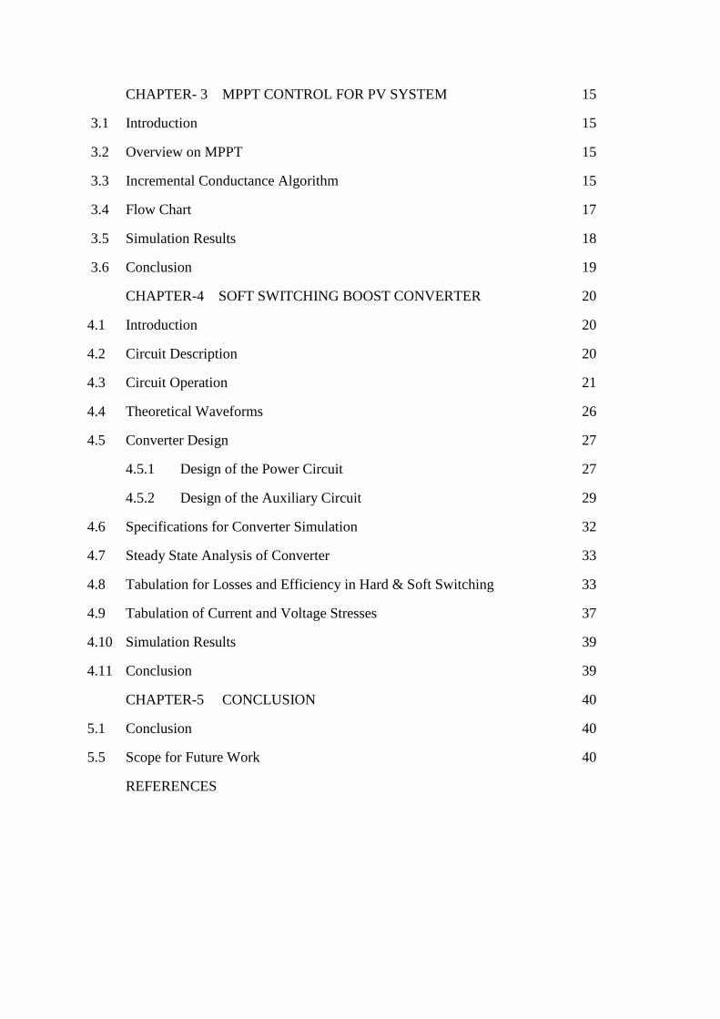
CHAPTER-4 SOFT SWITCHING BOOST CONVERTER
Introduction
Circuit Description
Circuit Operation
Theoretical Waveforms
Converter Design
4.5.1 Design of the Power Circuit
4.5.2 Design of the Auxiliary Circuit
Specifications for Converter Simulation
Steady State Analysis of Converter
Tabulation for Losses and Efficiency in Hard & Soft Switching
Tabulation of Current and Voltage Stresses
Simulation Results
Conclusion
20
20
20
21
26
27
27
29
32
33
33
37
39
39
5.1
5.5
CHAPTER-5 CONCLUSION
Conclusion
Scope for Future Work
REFERENCES
40
40
40

~ i ~
ABSTRACT
India is among leading power producing countries but still we have an unreliable and inefficient
electrical infrastructure. Photovoltaic power generation can be helpful to meet the requirements
of electricity demand. In order to increase efficiency of PV system a soft-switching boost
converter is adopted, which consists of an auxiliary resonant circuit having an auxiliary switch,
two diodes with a resonant capacitor and a resonant inductor. This model of converter can supply
60 W to load. Since hard switching generates losses during turn on and turns off but in the
proposed converter circuit Zero Voltage Switching operation is performed by resonant capacitor
at turn-off condition and Zero Current Switching operation by resonant inductor at turn-on. The
chosen converter reduces switching loss as well as voltage and current stress across the devices
due to this the efficiency of converter increases. As designed converter is operated at high
frequency, so small size of inductors and capacitors are required, this reduces size of converter.
Incremental Conductance algorithm is used to achieve maximum power from PV module .The
proposed converter and inverter circuit are simulated in Psim9.0 with PV and Maximum Power
Point Tracking and theoretical analysis is verified.

~ ii ~
LIST OF TABLES
Table. No.
Name of the table
Page. No.
2.1 Parameters of the simulated PV module
11
4.1 Component specifications of converter for simulation
27
4.2 Comparision of hard and soft-switching
38
4.3 Current and voltage stresses of various elements 39

~ iii ~
LIST OF FIGURES
Fig. No. Name of the Figure Page. No.
1.1 Loss of Power during hard switching 2
1.2
(a) ZVS MOSFET implementation at turn off
(b) Switching waveform of ZVS and hard switching
3
3
1.3 (a) ZCS MOSFET implementation at turn on
(b) Switching waveform of ZCS and hard switching
4
4
2.1 Block diagram of proposed PV system 7
2.2 Photovoltaic cell single diode model 8
2.3 Photovoltaic cell two diode model 9
2.4
2.5
2.6
Photovoltaic array
Current-Voltage curve for PV module
Power-Voltage curve for PV module
10
12
12
2.8 Variation of I-V curve with solar irradiation 13
2.9 Variation of P-V curve with solar irradiation 13
2.10 Variation in I-V curve with Temperature 14
2.11 Variation in P-V curve with temperature 14
3.1 P-V curve locating MPPT 16
3.2
3.3
3.4
3.5
Flow chart of IC MPPT
Current curve at MPP
Voltage curve at MPP
Tracking of maximum power of PV
17
18
18
19
4.1 Circuit diagram of soft switching boost converter 20
4.2 Equivalent circuit of mode 1 for interval [t0-t1] 21
4.3 Equivalent circuit of mode 2 for interval [t1-t2] 22
4.4 Equivalent circuit of mode 3 for interval [t2-t3] 23
4.5 Equivalent circuit of mode 4 for interval [t3-t4] 24
4.6 Equivalent circuit of mode5 for interval [t4-t5] 25
4.7 Equivalent circuit of mode6 for interval [t5-t6] 26
4.8 Theoretical waveforms of converter 26
~ iv ~
LIST OF ABBREVIATIONS
PV Photo Voltaic
ZVT Zero Voltage Transition
DC Direct Current
MOSFET Metal Oxide Semiconductor Field Effect transistor
PWM Pulse Width Modulation
EMI Electro-Magnetic Interference
ZVS Zero Voltage Switching
ZCS Zero Current Switching
MATLAB MATrix LABoratory
PSIM Powersim
MPPT Maximum Power Point Tracking
4.9 ZVS condition of switch 29
4.10 PWM signal for switch S1, S2 33
4.11 Main inductor current 34
4.12 Current and voltage across switch S1, S2 34
4.13 ZCS for switches S1, S2 at turn on 35
4.14
4.15
4.16
4.17
4.18
ZVS for switches S1, S2 at turn off
Resonant inductor current and resonant capacitor voltage
Output diode voltage and current
Output voltage of converter
Output power of converter
35
36
36
38
38

~ v ~
P&O Perturb and Observe
IC Incremental Conductance
LIST OF SYMBOLS
Ton Turn-on time of the switch
Toff Turn-off time of the switch
PSW Switching Power losses
VS Voltage blocked by the switch
IS Flow of current allowed by the switch
fS Switching frequency of the converter
Vin Input voltage
S1 Main switch/boost switch
S2 Auxiliary switch
L Boost inductor
Lr Auxiliary resonant inductor
Cr Auxiliary resonant capacitor
D1-D2 Auxiliary circuit diodes
D Boost diode
C0 Output capacitor
t0-t6 Time instants in one switching cycle

~ vi ~
ILr Current flowing through the auxiliary circuit
Vcr Voltage blocked by the resonant capacitor
Pout Output power rating
Vout Output voltage rating
Vrp Output voltage ripple
ΔIrp Input peak current ripple
η Efficiency of the converter
I_min Input min current
Imax Input max current
D Duty cycle
ΔD Duty Loss
fr resonant frequency
Zr Resonant impedance
IPV PV current
I0 Diode’s reverse saturation current
VT Diode’s thermal voltage
KI Temperature coefficient of Isc
KV Temperature coefficient of Voc
G Irradiance on the surface of the cell
GSTC Irradiance under STC
IPV_STC Photocurrent generated under Standard Test Conditions (STC)

~ vii ~
Eg Energy gap of the semiconductor
I0_STC Nominal saturation current
ISC_STC Nominal value of Isc
VOC_STC Nominal value of Voc
Nss Number of modules in a serial connected string
Npp Number of strings that are connected in parallel
Vmp Operating Voltage at MPP
Imp Operating Current at MPP
Pmax Maximum power
VH Unified voltage
a1 a2 Ideality constant of diode in two diode model
𝑎 Ideality constant of diode in single diode model

1
CHAPTER-1
INTRODUCTION
1.1 Overview
This work is intended towards developing a soft-switching boost converter which is useful for
Photovoltaic System. The main aim is to reduce switching losses by using a resonant circuit with
conventional boost converter. Here MPPT algorithm is used for extraction of maximum power to
ensure highly efficient operation of PV module. These converters consist of devices like diodes,
BJTs, MOSFETs and IGBTs, which are used as switching devices. There should be wise
selection of switching device depending upon power requirement and switching frequency.
MOSFET is best suited for low power and low voltage applications whereas IGBT is used for
higher power and higher voltage and current rating compared to MOSFET. IGBT’s are operated
in lower frequency range (up to 100 kHz) but MOSFET’s are operated at much higher frequency
range compared to IGBT. The proposed converter is operated under ZCS and ZVS condition
which ensures improved efficiency, less electromagnetic interference etc.
1.1.1 Losses in Switching Devices
The devices used for switching in converters does not behave as ideal in experimental
conditions, hence they are sources of loss of energy in the system. These losses are of two types
which are described below:
Conduction losses:
The basic devices used normally are IGBT and MOSFET. The conduction losses in case of
MOSFET are because of its nature of acting as resistor when it is fully turned on. The resistance
is between drain to source resistance represented as Rds. In case of IGBT the conduction loss
depends on current passing through device during turn on condition and voltage Vce,sat offered
across collector and emitter junctions.

2
Switching losses:
In practical conditions the voltage or current in the switch do not drops to zeros when it is
instantly turned on or off. So there is a time duration in which both current and voltages exists,
so we can say there is overlapping area of voltage and current curve of switching device.
Therefore this overlapping of curves causes power loss. Moreover as we know that average
power is proportional to the frequency, so higher switching frequency will cause more loss. One
more noticeable is the existence of EMI because of sharp and sudden transitions.
As it is clear from symbol of devices that both IGBT and MOSFET are having anti-parallel
diodes but MOSFET has higher value of capacitance between drain and source as compared to
capacitance between collector and emitter of IGBT. For MOSFET Cds is charged with off stage
voltage subjected to it and in case IGBT current tailing is observed even after turn off
condition. AS we can observe that main losses for MOSFET are because of charging and
discharging of the capacitance but for IGBT it is tailing current. The losses encountered in this
situation are called hard switching losses. The losses are shown in Fig. 1.1.
Fig. 1.1: Loss of Power during hard switching.
1.1.2 Soft Switching
The problems in case of hard switching like switching losses, EMI, current and voltage stresses
can be reduced by using soft-switching method. The term "soft-switching" is subjected to
gradual transitions of switch current and voltages. As transitions are gradual so 𝑑𝑖 𝑑𝑡⁄ and

3
𝑑𝑣 𝑑𝑡⁄ rating gets reduced so EMI reduction is observer and decrease is overlapping area
between current and voltage curves is also seen because soft-switching makes any of the current
or voltage to be zero when transition takes place. Therefore ideally there is no overlapping area
between current and voltage curves of the switching device. These switching techniques are of
two types: ZVS and ZCS. As in case of MOSFET it consists of capacitance Cds which is actually
combination of internal capacitance with additional external capacitance. MOSFET can be
turned on with ZVS when it is sure that voltage across the switch just before the turned on is
zero and MOSFET can turn off with ZVS because of Cds which prevents abrupt rise in the
voltage as the device is turned off [9]. Fig. 1.2 includes ZVS implementation using MOSFET
and its switching waveforms.
(a) (b)
Fig. 1.2: (a) ZVS MOSFET implementation at turn off
(b) Switching waveform of ZVS and hard switching
ZCS operation can be performed by the switch if an inductor is connected in series with it. ZCs
turn off can be achieved as inductor restricts rise in current which makes current through
MOSFET nearly to zero. MOSFET turn off switch ZCS is achieved when negative voltage
occurs across the combination (inductor-MOSFET) which causes gradual decay of current to
zero because of inductor [11]. Fig. 1.3 includes ZCS implementation using MOSFET and its
switching waveforms.

4
(a) (b)
Fig. 1.3: (a) ZCS MOSFET implementation at turn on
(b) Switching waveform of ZCS and hard switching
Both MOSFET and IGBT can be used to perform ZVS and ZCS but for MOSFET, ZVS is
preferred over ZCS and for IGBT ZCS is preferred over ZVS for IGBTs. When MOSFET is
used for ZVS it can reduce the losses because of discharging of Cds into device but in case of
ZCS it cannot be done. As for the IGBT its capacitance lower so its main loss is turn off loss due
to this tail in current is reduced witch ZCS method.
1.2 Literature Review
In conventional hard switching converters, the conduction losses are very low. But high
switching losses makes converters less efficient. So the technique of soft switching is introduced
to make the switching transitions at either zero voltage condition or zero current condition, so
that the dominating portion of losses (the ones caused due to switching under high voltages or
currents) can also be reduced and the efficiency of the converters can be highly improved.
A soft switching converter is designed and its utility for PV system converter is verified in [1].
Detailed analysis on calculation of conduction and switching losses is done for soft switching
boost converter and selection procedure of resonant element is discussed [2]. A review on
various topologies of soft switching converters is discussed and compared there efficiency and
other parameters. The discussion about isolated and non-isolated converters for PV system and
their suitability according to requirement is done. This detailed analysis of various circuits of
DC-DC boost converters on the basis of circuit complexity, efficiency is helpful for proper
selection of method for converter design [3]. Three different topologies buck, boost and buck

5
boost are discussed with their steady state analysis and design of the auxiliary and main circuits
are reported in [4]. A soft-switching inverter circuit is proposed which is operated with three
phase induction motor, this useful for reducing the losses in the PV system after the operation of
DC-DC converter [5]. A soft-switching converter using two switches main and auxiliary in
which auxiliary switch is operated with some delay from the main switch, the losses due to
switching for auxiliary switch reduces to zero. In this case higher voltage conversion ratio can be
obtained whereas controlling is difficult in this case [6]-[9]. Design of digital PID controller for
soft switching converters using pole placement technique is reported in [10]. Various ZCS
circuits are reported and their comparative analysis is done in the literature [11]. An analysis of
transformer less soft switching circuit with higher conversion ratio is proposed and their
comparison with isolated converters is reported in [12]. A review on soft switching inverter
circuits is presented in the paper [13]
Various papers have been referred soft switching methods for converter as well as for
Photovoltaic cell and MPPT. The comprehensive model for PV cell is proposed, the single diode
model and double diode is discussed , the equation related to this PV are derived, and the
variation of current, voltage and power with change of irradiation and temperature is studied
[14]-[16]. Incremental conductance MPPT is discussed and compared with other available MPPT
methods, it observed that better response for Incremental conductance algorithm is observed as
compared to Perturb and Observe algorithm. On the basis of complexity stability of MPP and
other parameters selection of algorithms is justified [17]-[22].
1.3 Motivation
In our country demand of power is increasing day by day but the production is not increasing in
that ratio. Electricity crises in summer season is very common but these are most hot days of the
year and in this duration solar radiation availability is at peak, so solar power generation can be
used more conveniently in this duration to fulfill the power requirement. The PV generation
system uses converter circuit, while using conventional hard switching converter circuit
efficiency of system reduces. This reduction in efficiency is due to switching loss, energy loss in
stray L and C, device stress, thermal management, reverse recovery characteristics of diode. To
overcome these losses, design soft switching converter circuit is the best among available
solutions.

6
1.4 Objectives
The main objectives of this work are-
1. Reduction in power losses due to switching of MOSFETS by using soft switching cell.
2. Reduction in voltage stress and current stress of the switches and diodes.
3. Reduction in EMI problem caused by high 𝑑𝑖
𝑑𝑡 and
𝑑𝑣
𝑑𝑡 rating by proper selection of resonant
elements.
4. Simulation of proposed system and verification of theoretical analysis.
1.5 Thesis Organization
This thesis is manifested in chapter wise as follows:
Chapter 1
An overview of selection of soft switching technique over hard switching and renewable energy
sources over other sources for power generation. Advantages soft switching over hard switching
converters are listed. The motivation and objectives for this project are included.
Chapter 2
A brief discussion on proposed system, PV cell modeling with proper equivalent circuit and
equations. PV characteristics and its variation with temperature and irradiation are explained
with simulation results.
Chapter 3
An introduction to MPPT and its importance in solar PV power generation is presented. Mainly
IC algorithm is presented in detail and simulation output of MPPT is discussed.
Chapter 4
A detailed analysis on soft switching boost converter and its need in solar power generation
system is presented. The converter operation in six modes and corresponding equation are given.
Simulation result of converter circuit with PV and MPPT is presented in this chapter.
Chapter 5
Conclusion of work done and futures aspect of the work is included.

7
CHAPTER 2
PHOTOVOLTAIC SYSTEM
2.1 Introduction
This chapter deals with the Photovoltaic system. A photovoltaic system is basically consist of
few or large number of solar panels to get electrical energy from solar energy. It is composed of
various component such as PV modules, mounting, mechanical and electrical connections and
means of regulating output voltage of the system.
2.2 Arrangement of Proposed PV System
The PV system with MPPT is shown in the Fig. 2.1. The output voltage of PV is given to the
converter, the current and voltage values are given to MPPT block which accordingly changes
the duty cycle of pulses to extract maximum power. The obtained duty cycle given to PWM
generator and it generates pulses, which are given to gate terminal of MOSFET switches.
SOFT-SWITCHING CONVERTER
LOADPV
MPPTPWM
GENRATOR
Duty Cycle
Pulses
Fig. 2.1: Block diagram of proposed PV system

8
2.3 Mathematical Representation of PV
A PV cell can be represented mathematically by single and double diode models which are
described below:
2.3.1 Single Diode Model
The single diode model [14] is shown below in Fig. 2.2 for a PV cell which includes a current
source 𝐼𝑃𝑉 with a diode and a resistance in parallel and this structure is in series with
resistance 𝑅𝑠 .
V
D
Ipv
ID
I
RS
RP
+
-
Fig. 2.2: Photovoltaic cell single diode model
The load current equation is given by
P
S
T
SPV
R
IRV
aV
IRVIII 1exp0
……………………………………………..… (2.1)
In above equation IPV represents photo current and Io is reverse saturation current which are
given by equations (2.2) and (2.3).
STC
ISTCPVPVG
GTKII _ ………..……………………………………………….……… (2.2)
TTak
qE
T
TII
STC
gSTCSTC
11exp
3
_00…………………………………………...……… (2.3)
The equation (2.3) can be modified to (2.4) in terms of coefficients of current and voltages 𝐾𝐼
and 𝐾𝑉 as follows:

9
1/exp _
_
0
TVSTCOC
ISTCSC
aVTKV
TKII ………………………………………………...……… (2.4)
2.3.2 Double Diode Model
The single diode model neglects the recombination losses in depletion region. In actual practice
these recombination losses causes a substantial loss, especially low voltages. This modeling is
not possible using single diode model. To consider losses more precise two-diode model [15] is
required, which is shown in Fig. 2.3.
V
D1 D2
Ipv
ID1ID2
I
RS
RP
+
-
Fig. 2.3: Photovoltaic cell two diode model
The equations modelled for single diode model can be modified to get current expression for
double diode model.
P
S
T
S
T
SPV
R
IRV
Va
IRVI
Va
IRVIII 1exp1exp
21
0201……………………..… (2.5)
Where
1exp
1
011
T
Sd
Va
IRVII ………………………………………………….…………..… (2.6)
1exp
2
022
T
Sd
Va
IRVII ……………………………………………………………...… (2.7)
STC
ISTCPVPVG
GTKII _ ……………………………………………………….……..… (2.8)

10
1}/{exp21
_
_
0201
TVSTCOC
ISTCSC
Vp
aaTKV
TKIII ……………..……… (2.9)
The diode ideal factors 1a and 2a represents recombination and diffusion components and on the
basis of Shockley equation the value of 1a is unity whereas value of 2a is flexible. On the basis
of simulations it can be found that 2a is 1.2, so we can conclude
1
21
p
aa . So equation (2.9)
can be rewritten as
1/exp _
_
0201
TVSTCOC
ISTCSC
VTKV
TKIII ………………………… …… (2.10)
2.3.3 Large Array Simulation
For large power applications a series parallel structure (i.e. Nss × Npp modules), as shown in Fig.
2.4. The equation for PV can be modified as shown in equation (4.10) for single diode model
[15].
Fig. 2.4: Photovoltaic array
PP
SSP
PP
SSS
SST
PP
SSS
PPPPPV
N
NR
N
NIRV
NaV
N
NIRV
NINII 1exp0 ………………………. (2.11)
11
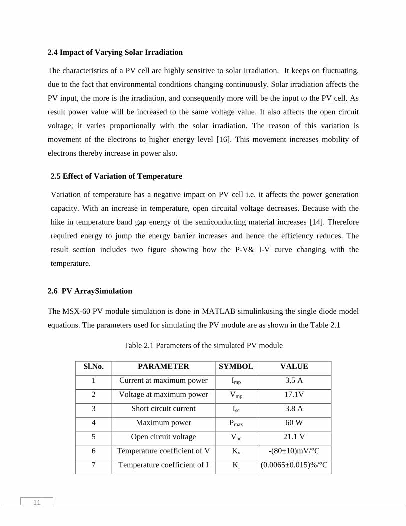
2.4 Impact of Varying Solar Irradiation
The characteristics of a PV cell are highly sensitive to solar irradiation. It keeps on fluctuating,
due to the fact that environmental conditions changing continuously. Solar irradiation affects the
PV input, the more is the irradiation, and consequently more will be the input to the PV cell. As
result power value will be increased to the same voltage value. It also affects the open circuit
voltage; it varies proportionally with the solar irradiation. The reason of this variation is
movement of the electrons to higher energy level [16]. This movement increases mobility of
electrons thereby increase in power also.
2.5 Effect of Variation of Temperature
Variation of temperature has a negative impact on PV cell i.e. it affects the power generation
capacity. With an increase in temperature, open circuital voltage decreases. Because with the
hike in temperature band gap energy of the semiconducting material increases [14]. Therefore
required energy to jump the energy barrier increases and hence the efficiency reduces. The
result section includes two figure showing how the P-V& I-V curve changing with the
temperature.
2.6 PV ArraySimulation
The MSX-60 PV module simulation is done in MATLAB simulinkusing the single diode model
equations. The parameters used for simulating the PV module are as shown in the Table 2.1
Table 2.1 Parameters of the simulated PV module
Sl.No. PARAMETER SYMBOL VALUE
1 Current at maximum power Imp 3.5 A
2 Voltage at maximum power Vmp 17.1V
3 Short circuit current Isc 3.8 A
4 Maximum power Pmax 60 W
5 Open circuit voltage Voc 21.1 V
6 Temperature coefficient of V Kv -(80±10)mV/°C
7 Temperature coefficient of I Ki (0.0065±0.015)%/°C
12
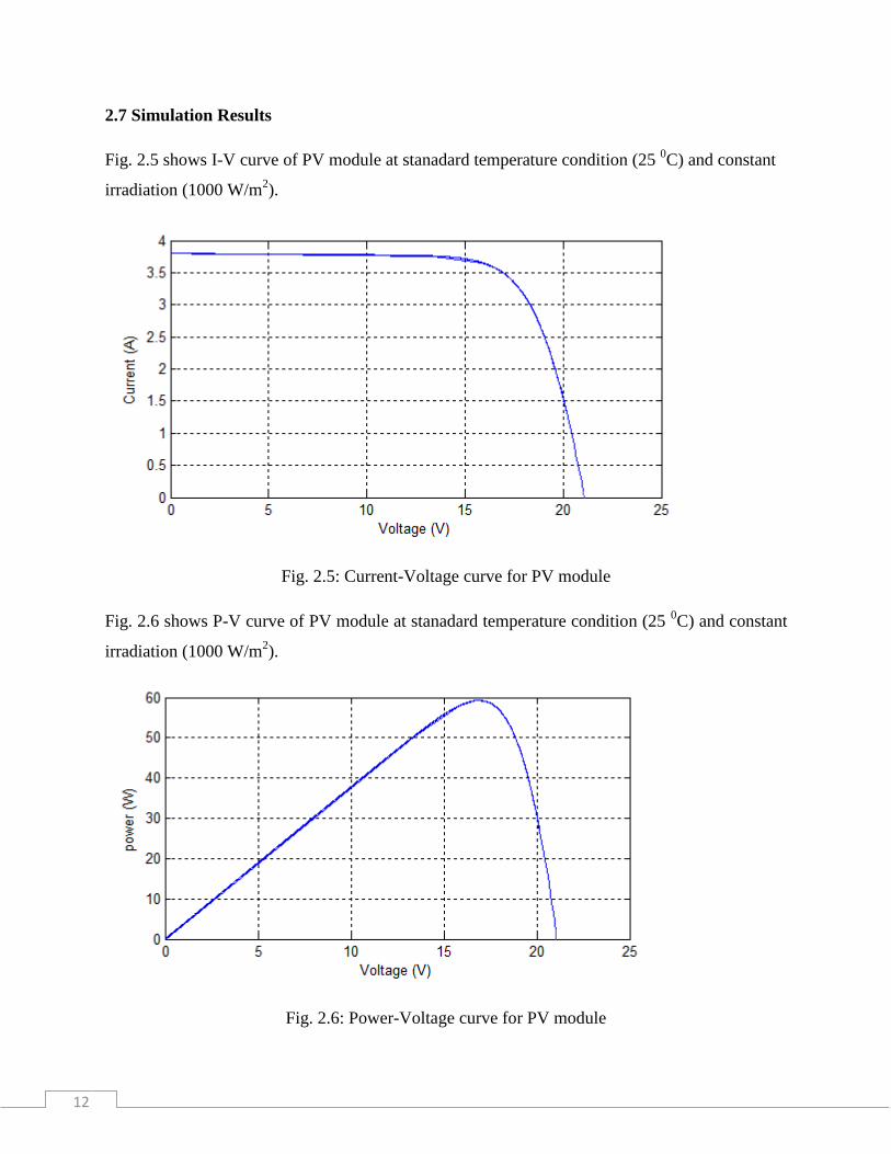
2.7 Simulation Results
Fig. 2.5 shows I-V curve of PV module at stanadard temperature condition (25 0C) and constant
irradiation (1000 W/m2).
Fig. 2.5: Current-Voltage curve for PV module
Fig. 2.6 shows P-V curve of PV module at stanadard temperature condition (25 0C) and constant
irradiation (1000 W/m2).
Fig. 2.6: Power-Voltage curve for PV module

13
Fig. 2.7 shows I-V curve of PV module at stanadard temperature condition (25 0C) and varying
irradiation 1000 W/m2, 800 W/m
2 and 600 W/m
2 respectively.
Fig. 2.7: Current-Voltage curve with variation of irradiation
Fig. 2.8 shows P-V curve of PV module at stanadard temperature condition (25 0C) and varying
irradiation 1000 W/m2, 800 W/m
2 and 600 W/m
2 respectively.
Fig. 2.8: Power-Voltage curve with variation of irradiation
Fig. 2.9 shows I-V curve of PV module at constant irradiation (1000 W/m2) and varying
temperature 25 0C.
G=600 𝑊
𝑚2
G=800 𝑊
𝑚2
G=1000 𝑊
𝑚2
G=600 𝑊
𝑚2
G=800 𝑊
𝑚2
G=1000 𝑊
𝑚2

14
Fig. 2.9: Current-Voltage curve with variation of temperature
Fig. 2.10 shows P-V curve of PV module at constant irradiation (1000 W/m2) and varying
temperature 25 0C
Fig. 2.10: Power-Voltage curve with variation of temperature
2.8 Conclusion
This chapter illustrates the basic idea on PV. Two different model of PV are discussed. PV
model is properly described using equivalent circuit diagram along with all the relevant equation.
The parameters taken during simulation listed in a table. The simulation results of P-V and I-V
characteristics are included.
T= 60℃
T= 45℃
T= 25℃
T= 60℃
T= 45℃
T= 25℃

15
CHAPTER-3
MPPT CONTROL FOR PV SYSTEM
3.1. Introduction
This chapter mainly discuss about the Maximum power point tracking circuit. Types and process
of tracking are described here. It gives mainly basic idea on Incremental conductance method
with flow chart.
3.2 Overview on MPPT
PV system’s efficiency depends on MPPT. MPPT is the most important in PV system. The
efficiency of a PV system largely depends on MPPT and main cause of shifting of MPP
(Maximum Power Point) is change in temperature and irradiation given to the PV [17].
Moreover it is clear that PV has nonlinear characteristics so it becomes more necessary to use
MPPT.
There are various methods available for the tracing of MPPT some of them are named below:
1. Perturb and observe method
2. Incremental conductance algorithm
3. Fuzzy logic control method
4. Fractional open circuit voltage
5. Fractional short circuit current etc.
Here “Incremental conductance” is selected for proposed PV system as it gives more rapid
response as compared to P&O method and less oscillation.
3.3 Incremental Conductance Algorithm
This algorithm is used to conclude the sign of 𝑑𝑃
𝑑𝑉 ratio and continuous observes the dynamic
conductance (∆I/ ∆V) and it is compared with the static conductance (I / V) when both becomes

16
equal then MPP is achieved [18]. A set of mathematical equation can be written for more ease of
understanding as:
The power is given by VIP ………………………………………………….………….. (3.1)
dV
dIII
dV
dIV
dV
dVI
dV
VId
dV
dPI
)(………………………………………..………. (3.2)
So equations can be expressed as
V
I
dV
dI Or 0
dV
dP At MPP ………………………………………………...………… (3.3)
V
I
dV
dI Or 0
dV
dPLeft of MPP…………………………………...……………......…….. (3.4)
V
I
dV
dI Or 0
dV
dPRight of MPP…………………………………..……….....……...…… (3.5)
The above three equations from equation (3.3) to equation (3.5) describes the position of
MPP with respect to slope of P-V or I-V curves. Fig. 3.1 is graphical representation of above
equations.
I
V
V
I
dV
dI
V
I
dV
dI
V
I
dV
dI
Fig. 3.1: I-V curve locating MPPT
17
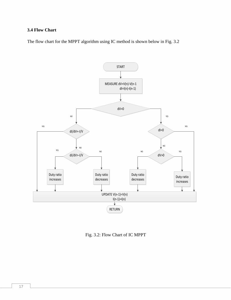
3.4 Flow Chart
The flow chart for the MPPT algorithm using IC method is shown below in Fig. 3.2
START
dV=0
dI/dV=-I/V dI=0
dI/dV>-I/V dV>0
MEASURE dV=V(n)-V(n-1 dI=I(n)-I(n-1)
Duty ratio increases
Duty ratio decreases
Duty ratio decreases
Duty ratio increases
UPDATE V(n-1)=V(n) I(n-1)=I(n)
RETURN
NO YES
YES
YESNO
NO
YES
YESNO
NO
Fig. 3.2: Flow Chart of IC MPPT

18
3.5 Simulation Results
MPPT output of the PV system is shown below. Fig. 3.3 shows current of PV at maximum
power point. Initially current fluctuates and later it goes steady. The obtained vale of current at
MPP is 3.68 A, which can be observed in Fig. 3.3.
Fig. 3.3: Current curve at MPP
Fig. 3.4 shows voltage at MPP, initially voltage rises from zero and later goes steady. Here
voltage at MPP is 17.1 V.
Fig. 3.4: Voltage curve at MPP

19
Fig. 3.5 shows power curve at MPP. Two labels for output tracked power curve of PV and
maximum rated power curve of PV module. The obtained power at MPP is 59.5 W.
Fig. 3.5: Tracking of maximum power of PV
3.6 Conclusion
With the end of this chapter, it can be concluded that, MPPT is an important part for the PV
system. As the curves obtained from PV system are nonlinear. Incremental conductance method
is successfully demonstrated here with corresponding simulation results, relevant equation and
flow diagram.

20
CHAPTER-4
SOFT SWITCHING BOOST CONVERTER
4.1 Introduction
This chapter gives an idea on soft switching boost converter. There are many DC-DC converters
are available. For stepping up the voltage to some certain level, boost converter required. And
the boost converter using soft switches make the whole system more efficient. How it increases
the efficiency and details on soft switching technique are discussed.
4.2 Circuit Description
The circuit for soft switching converter is shown in Fig. 4.1 which consists of an extra soft-
switching circuit which is not present in case of conventional boost converter. The auxiliary
network comprises of an auxiliary switch (𝑆2) two diodes named as (𝐷1) and (𝐷2), resonant
capacitor (𝐶𝑟) and resonant inductor (𝐿𝑟) , whereas main circuit composed of main
inductor (𝐿𝑚), main switch(𝑆1), output capacitor (𝐶𝑜) and Load (𝑅). Supply is denoted as (𝑉𝑖𝑛)
which is actually voltage generated by PV and output voltage marked across load as indicated in
Fig. 4.1
Vin
L
Lr
S1
Do
CoCr
D1
D2
R
+
VO
-
S2
Fig. 4.1: Circuit diagram of soft switching boost converter

21
4.3 Circuit Operation of Soft-Switching Converter
The circuit for soft switching converter is operated in six modes [1]. The operation of the circuit
in different modes is described below along with circuit diagrams and respective equations of
those modes.
Mode 1 in the interval [t0-t1]
In mode 1 converter operates like conventional hard-switching converter and during this mode
main and auxiliary switches 𝑆1 and 𝑆2 is in OFF condition. Current does not flows through
resonant circuit but the load gets energy from the main inductor and main inductor current
decreases linearly which is visible in waveforms shown in Fig. 4.2. Circuit and equations for this
mode are shown below
oSL VVtV )( ……………………………………………………………………...………… (4.1)
tL
VVtItI So
LL
)()( 0 ………………………………………………………………..…... (4.2)
)()( tItI LDo …………………………………………………………………..……….……. (4.3)
0)( tILr ……………………………………………………………………………….…….. (4.4)
oCr VtV )( …………………………………………………..……………………….……...... (4.5)
Vin
L
Do
Co R
+
VO
-
ILIDo
Fig. 4.2: Equivalent circuit of mode 1 for interval [t0-t1]

22
Mode 2 in the interval [t1-t2]
In this mode two switches 𝑆1 and 𝑆2 are turned on under ZCS due implementation of ZCS by
main and auxiliary switches losses decreases. Here current through resonant inductor rises in this
mode which results decrease in load current, when circuit operates at time 2t current passing
through diode 𝐷𝑜 . Circuit diagram for this mode is shown in Fig. 4.3 and equation are shown
below
0)( 1 tILr , oLr VtV )( ………………………………………………………...………...…. (4.6)
tL
VtI
r
oLr
)( ……………………………………………………………..…………………. (4.7)
tL
VVtItI So
LL
)()( 1 ………………………………………………………..….……….. (4.8)
)()( 22 tItI LrL ………………………………………..…………………………....……….... (4.9)
0)( 2 tIDo ……………………………………………………………………….......…….... (4.10)
Vin
L
Lr
S1
Do
Co R
+
VO
-
S2
IL IDo
ILr
Fig. 4.3: Equivalent circuit of mode2 for interval [t1-t2]
23
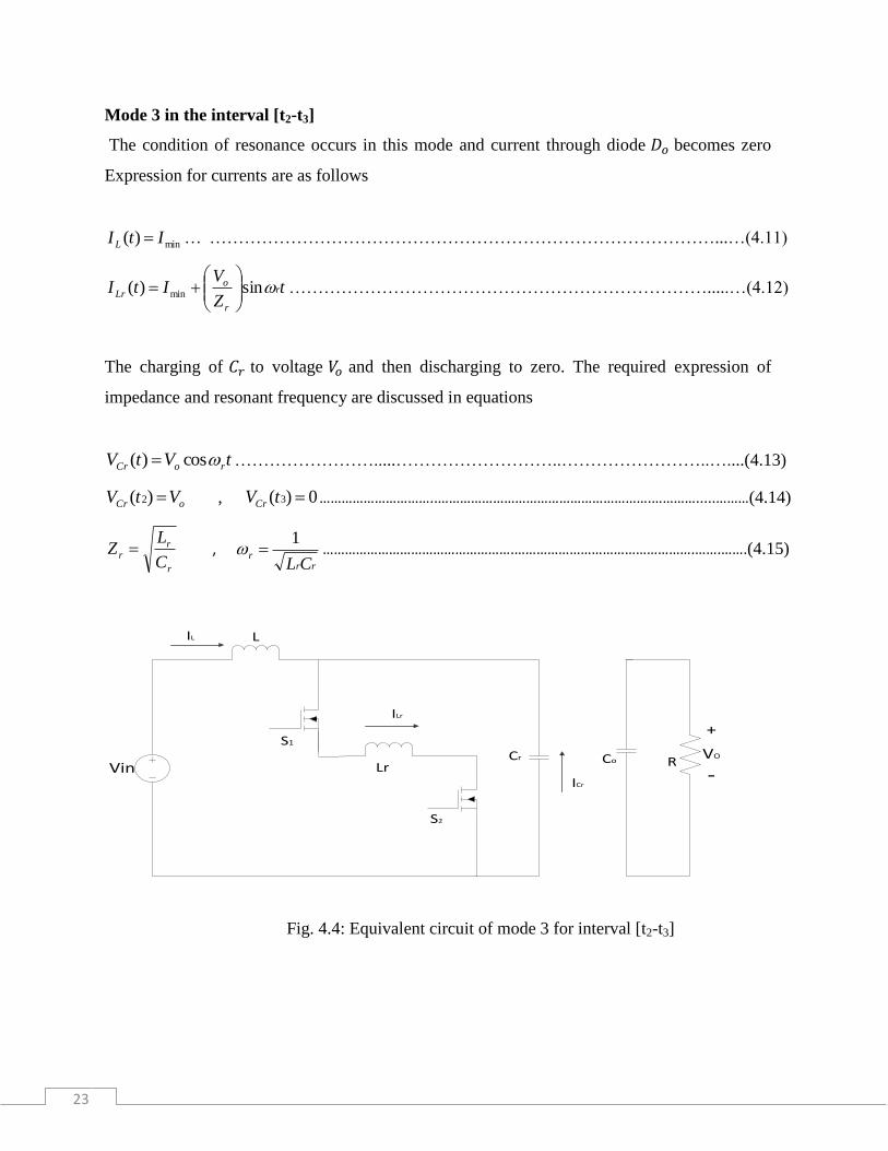
Mode 3 in the interval [t2-t3]
The condition of resonance occurs in this mode and current through diode 𝐷𝑜 becomes zero
Expression for currents are as follows
min)( ItIL … ……………………………………………………………………………...…(4.11)
tZ
VItI r
r
oLr sin)( min
……………………………………………………………….....…(4.12)
The charging of 𝐶𝑟 to voltage 𝑉𝑜 and then discharging to zero. The required expression of
impedance and resonant frequency are discussed in equations
tVtV roCr cos)( …………………….....………………………..……………………..…....(4.13)
oCr VtV )( 2 , 0)( 3 tVCr …………………………..………………………………………………….………….....………(4.14)
r
rr
C
LZ ,
rrr
CL
1 …………………………………………….………………………………………….…….…….(4.15)
Vin
L
Lr
S1
CoCr R
+
VO
-
S2
IL
ILr
ICr
Fig. 4.4: Equivalent circuit of mode 3 for interval [t2-t3]

24
Mode 4 in the interval [t3-t4]
This mode operates in ZVS condition as current through resonant inductor is higher than main
inductor both diodes of auxiliary circuits are in ON state. Path of current flow in circuit
diagram shown in Fig. 4.5. Equations for resonant inductor and main inductor current and
voltages are from equation (4.16) to equation (4.19).
)()()()(21
tItItItI DDLLr ………………………………………………………………..(4.16)
max,43 )()( LrLrLr ItItI ……………………………………………………………………..(4.17)
SL VtV )( ……………………………………………..…………………………………..(4.18)
tL
VItI S
L
min)( ………………...………………………………………………………..(4.19)
Vin
L
Lr
S1
Co
D1
D2
R
+
VO
-
S2
ILr
ILD2
ID1
IL
Fig. 4.5: Equivalent circuit of mode 4 for interval [t3-t4]
Mode 5 in the interval [t4-t5]
In this mode both switches are in OFF condition due to zero voltage condition of resonant
capacitor. The voltages and currents for various elements in this mode are as follows:
tIIItI rLrLr cos)()( maxmax,max ………………………………………………………......(4.20)
max,4 )( LrLr ItI ………………………………………………………………………….….....(4.21)
0)( 4 tVCr ………………………………………………………………………….…..….…(4.22)

25
max)( ItIL ………………………………………………………………………….....….. (4.23)
tIIItI rLrLr cos)()( maxmax,max …………………………………………………………...(4.24)
tIIZtV rLrrCr sin)()( maxmax, …………………………………………….…………….…..(4.25)
Vin
L
LrCo
D1
D2
R
+
VO
-
ILr
ILD2
ID1
IL
Cr
ICr
Fig. 4.6: Equivalent circuit of mode5 for interval [t4-t5]
Mode 6 in the interval [t5-t6]
It can be observed clearly that in the start of this mode the voltage across resonant capacitor
reaches equal to output voltage, in another consequence output diode is turned on due to zero
voltage condition.
)()()( tItItI LrLDo ……………….………………………………………………….….……..(4.26)
max45(maxmax,5 )cos)()( IttIItI rLrL ……………..………………………….……………..(4.27)
oCr VtV )( ……………………………………….………………………………………………..(4.28)
Further decrease in main inductor and resonant inductor currents is observed and transfer of
complete energy of the inductor to load through diode 𝐷𝑜 takes place.
tL
VVItI
r
SoL
max)( ………………………………………………………………………....(4.29)

26
tL
VtItI
r
oLrLr
)()( 6 ……………………………………………………………………….…..(4.30)
0)( 6 tIL ………………………………………….………………………………………….…...(4.31)
Vin
L
LrCo
D1
D2
R
+
VO
-
ILr
ILD2
ID1
IL
Do
IDo
Fig. 4.7: Equivalent circuit of mode6 for interval [t5-t6]
4.4 Theoretical Waveforms
The Fig. 4.8 shows theoretical waveforms for one switching cycle. The theoretical curves for gate
pulses, diode current, switch current and voltages, resonant inductor current and resonant capacitor
voltage [4].
t t t ttt t0 1 2 43 5 6
S1,S2
i
L
Lr
i
i d
vCr
vvS1 S2
i ,iS1 S2
Imin
I Lrmax
Imax
Vo
Vo
Fig. 4.8: Theoretical waveforms of converter

27
4.5 Converter Design
The specifications for the design of the converter are given in table 4.1. The specifications
include converter output power rating, input voltage range, output voltage, allowable ripple
percentage in current and voltage etc. Design of circuit includes two steps power circuit and
auxiliary circuit respectively.
Table 4.1 Converter specifications for design
Sl. No. Parameter Specification Value
1 Output power P0ut 60W
2 Output voltage V0ut 42V
3 Input voltage Vin 15-25V
4 Switching frequency Fsw 50kHz
5 Output voltage ripple ΔV0 5%
6 Input current peak ripple ΔIL 20%
4.5.1 Design of the Power Circuit
The power circuit consists of the main switch, boost diode, input inductor and the output
capacitor. Here calculations for input inductor and output capacitor are shown.
Input inductor L:
The numerical value of the input inductor 𝐿 must be decided first because its value sets the peak
input current which the converter switches have to withstand and therefore this current is
necessary to decide the rating of other power circuit components [3]. The maximum current
without ripple is
AV
P
Iin
ut
34.415
92.0
60
min
0
max
…………………………………………………..……….…... (4.32)

28
The maximum peak-peak ripple current is
AIIII pkLrpp 869.0%2034.4max_ ………………………………..…….….. (4.33)
Therefore the maximum peak input current with ripple is
AI
IIrpp
pkrpk 774.42
869.034.4
2max_max_
…………………………………….….. (4.34)
The duty ratio of the converter when the maximum current occurs is
6428.042
1511
0
min_
max V
VD
in………………………………..………………….…... (4.35)
The input inductor value is calculated as follows
HkHzfI
DVL
swL
in240
50832.0
6428.015maxmin_
……………………………………..…….…... (4.36)
Output capacitor:
The output capacitor acts as an energy storage element. It stores energy when the input voltage
and current are near their peak and provides this energy to the output load when the line is low.
The point of reference for selection of capacitor is the endurable ripple in the output voltage. The
peak charging current of the capacitor is
AV
PII
ut
ut
Opkchg 428..142
60
0
0
_ ………………………………………….………….….. (4.37)
The output capacitor C0 can be determined by
………………………………………………….…………………...…... (4.38)
os
o
VRf
VDC
)1(
29
os
o
Vf
IDC
)1(………………………………………………………………………...……. (4.39)
)4205.0(1050
428.142
251
C …………………………………………………………..………. (4.40)
4.5.2 Design of the auxiliary circuit
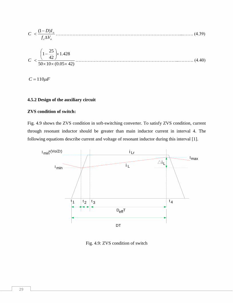
ZVS condition of switch:
Fig. 4.9 shows the ZVS condition in soft-switching converter. To satisfy ZVS condition, current
through resonant inductor should be greater than main inductor current in interval 4. The
following equations describe current and voltage of resonant inductor during this interval [1].
DT
DeffT
i L
Imax
min
minI
+(Vo/Zr)
tt tt1 2 3 4
I
i L
Lri
Fig. 4.9: ZVS condition of switch
FC 110

30
……………………………………………………………………...…. (4.41)
404.042
2542min
D
o
ino
V
VVD
min,
max ……………………………..…………………………………………. (4.42)
6428.042
1542max
D
FWFsatDSLr VVVtV ,)( …………………………………………………………...…..…. (4.43)
maxmin)( IZ
VIt
L
VtI
r
O
r
FW
Lr ………………………………………………………….. (4.44)
maxminmax)( IZ
VITD
L
VtI
r
O
r
FW
Lr . ………………………….……………………….. (4.45)
L
r
O
r
FW
L IZ
VTD
L
VIII maxminmax ………………………………………….……… (4.46)
Resonant inductor:
In Fig. 4.9, the time interval 2 is the rising time of resonant inductor current given by equation
(4.47). To get maximum resonant current, the time interval 3, is selected as ¼ of the resonant
period given by equation (4.48). For proper selection of resonant inductor, interval 2 and
interval 3 collectively can be set to 10% of minimum on time period. Sometime it is selected as
50% of minimum on time [6].
min23 IV
Ltt
O
r …………………………………………………………………………….. (4.47)
434
rTtt . ……………………………………………………………….……………….. (4.48)
o
ino
V
VVD
max,
min

31
TDT
IV
L r
O
r
minmin 1.04 ………………………………………………………………….… (4.49)
min
maxmin
2
2
II
TDVTVD
L
L
FWo
r
………………………………………………………………. (4.50)
52.22
832.0
1050
6428.01.2-42
1050
1404.0
233
rL …………………………………..……... (4.51)
HLr 10
Resonant capacitor:
The resonant capacitor is connected in parallel to the switch, so voltage of resonant capacitor and
main switch will be similar at turn-off condition. To satisfy ZVS condition, it can be selected ten
times of the output capacitance of the switch [1]. Simplified equation for resonant capacitor is
given by equation (4.4)
oo
r
r
o
rV
TDI
V
LI
L
VTDC
2
minmin
22
min2
2
2min
2 8.0404.0
………………………………….………. (4.52)
42
1050
1404.52.28.0
42
1052.24
10
421050
1404.004.0
2
3
22
52
52
2
2
rC
nFCr 40

32
4.6 Steady State Analysis of Converter
The output voltage of converter can be obtained by averaging voltage path of diode and inductor
over a switching period [4]. The output voltage is assumed to a constant voltage source and can
be derived as follows:
iTLTDo VVavgVavgV }{}{ ……………………………………………...……………… (4.53)
Where diode voltage average can be calculated as
T
ZI
VZIVCZI
ttVCLV
Vavg
r
rL
H
rLHrrL
HrrH
TD
122
)12
}{
35(
…………… (4.54)
Similarly inductor averaged voltage can be derived, above observation shows that design of
output voltage is more difficult in case of soft switching techniques
H
TDeff
V
VavgD
}{ ……………………………………………………………………………. (4.55)
T
VZIVZiZiZIV
V
VLi
D
rH
rLHrLrL
r
rLH
H
H
rL
2442
arcsin22
………………….. (4.56)
The output voltage of proposed converter in terms of effD is given by
i
eff
o VD
V \1
1
…………………………………….………………………….…...……….. (4.57)
33
4.7 Specification of converter for Simulation
Table 4.1 includes specifications of converter which are used for simulating the circuit in
Psim9.0.
Table 4.1 Converter specfication for simuation
Sl. No. Parameter Specification Value
1 Output power P0ut 60W
2 Output voltage V0ut 42V
3 Input voltage Vin 15-25V
4 Switching frequency Fsw 50kHz
5 Resonant inductor Lr 10 µH
6 Resonant capacitor Cr 40nF
7 Main inductor L 240µH
8 Output capacitor C0 110µF
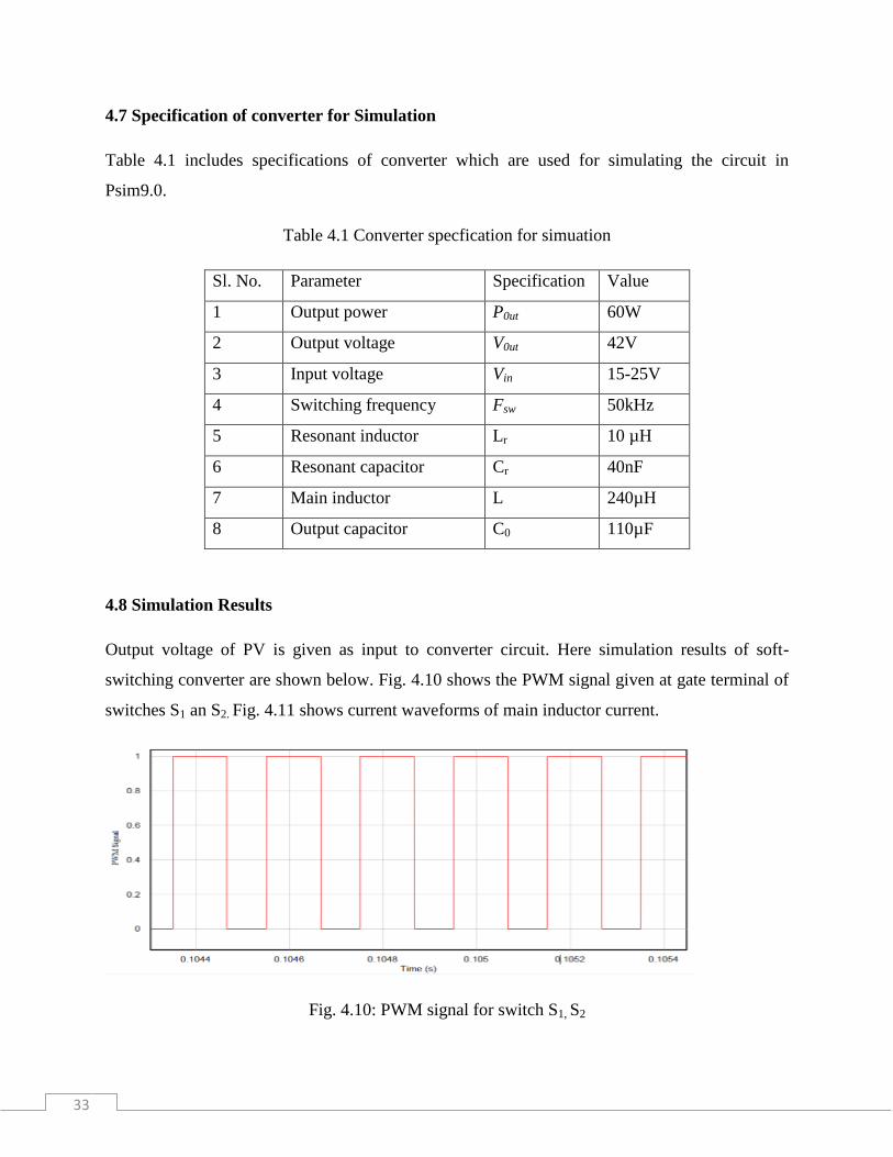
4.8 Simulation Results
Output voltage of PV is given as input to converter circuit. Here simulation results of soft-
switching converter are shown below. Fig. 4.10 shows the PWM signal given at gate terminal of
switches S1 an S2. Fig. 4.11 shows current waveforms of main inductor current.
Fig. 4.10: PWM signal for switch S1, S2

34
Fig. 4.11: Main inductor current
Fig. 4.12 shows voltage and current waveforms of switchesiS1 and S2 representing soft switching
operation of switches.
Fig. 4.12: Current and voltage across switch S1, S2
Fig. 4.13 showsiswitchesiS1 and S2 are turned on with ZCS. Here switch voltage changes 20V to
zero whereas current is slowly rising due to linearly charged resonant inductor.

35
Fig. 4.13: ZCS for switches S1, S2 at turn on
Fig 4.14 shows switches S1 and S2 are turned on with ZCS. Here switch current changes 6A to
zero whereas voltage is slowly rising due to linearly charged resonant capacitor.
Fig. 4.14: ZVS operation for switches S1, S2 at turn off
Fig. 4.15 shows curve of resonant inductor current and resonant capacitor voltage, these elements
make circuit to operate in resonance in mode 3 of operation. Fig. 4.16 shows the diode current
and voltage waveforms simultaneously.

36
Fig. 4.15: Resonant inductor current and resonant capacitor voltage
Fig. 4.16: Output diode voltage and current
Fig. 4.17 shows the output voltage waveform of soft switching converter which is obtained
approximately 42 V when 21 V from PV given as input with duty ration of 0.5 and 50 kHz of
switching frequency. The efficiency of converter at full load is 95.9 %. Fig. 4.18 shows the
output power of the converter at full load. The power at full load is 57.43 W.

37
Fig. 4.17: Output voltage of converter
Fig. 4.18: Output power of converter
4.9 Tabulation for losses and efficiency in hard and soft switching
There are two types of losses which occur in soft-switching converter which are switching and
conduction losses for calculation of these losses following formulas are used:
For calculation of switching losses in main and auxiliary switch
200
offon
swsw
TTFIVP
For calculation of conduction losses in main and auxiliary switch
onrmsscondsw RIP 2
__ 8.1
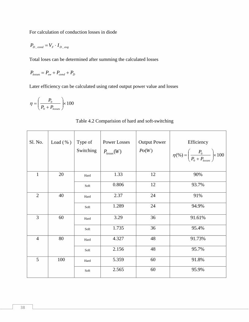
38
For calculation of conduction losses in diode
avgDFcondD IVP __
Total loses can be determined after summing the calculated losses
Dcondswlosses PPPP
Later efficiency can be calculated using rated output power value and losses
1000
0
lossesPP
P
Table 4.2 Comparision of hard and soft-switching
Sl. No.
Load ( % )
Type of
Switching
Power Losses
)(WPlosses
Output Power
)(WPo
Efficiency
100(%)0
0
lossesPP
P
1 20 Hard 1.33 12 %90
Soft 0.806 12 %7.93
2 40 Hard 2.37 24 %91
Soft 1.289 24 %9.94
3 60 Hard 3.29 36 %61.91
Soft 1.735 36 %4.95
4 80 Hard 4.327 48 %73.91
Soft 2.156 48 %7.95
5 100 Hard 5.359 60 %8.91
Soft 2.565 60 %9.95

39
4.10 Tabulation for current and voltages stresses
The switching stresses in various element is calculated and tabulated in
Table 4.3 Current and voltage stresses of various elements
Sl. No. Specification Calculated Values
1
baseI
AI 34.4max
2
baseV
VVo 42
3
Voltage stresses of S1, S2, D1,
D2 and Do
).(0.1 up
4
Current stresses of S1, S2, D1,
and D2
).(17.10.1max
upI
L
CV
r
r
o
5
Current stress of Do ).(17.20.2max
upI
L
CV
r
r
o
4.11 Conclusion
In chapter soft switching boost converter is discussed. Operation modes with block diagram of
the proposed system are illustrated. Theoretical waveform presenting the operational intervals is
described. Simulation results of circuit with PV and MPPT is presented. Efficiency calculation is
done for converter circuit and tabulated, which shows higher efficiency for soft switching
converter.

40
CHAPTER-5
CONCLUSION
5.1iConclusion
In this project simulation and design of soft switching converter is done. Efficiency of hard
switching and soft switching converters are compared at varying load conditions, in which
efficiency for designed soft switching converter is found to be much higher. Switching curves for
converter circuit. Switching curves for soft-switching circuit are gradual which decreases 𝑑𝑖 𝑑𝑡⁄
and 𝑑𝑣 𝑑𝑡⁄ rating and hence reduction in EMI achieved.
5.2 Scope for Future Work
In further work, proposed converter can be used as interleaved boost converter by connecting
two such converters in parallel, this connection may result more increase in efficiency. A PID
controller can be designed for the converter circuit for more stabilized output and its robustness
can be verified. To get isolation without using transformers, coupled inductor topology can be
constructed using designed circuit. The designed circuit can be used in stand-alone and grid
connected PV system. The circuit can be used for power factor correction by slight modification.

41
REFERENCES
[1] S.H. Park, G.R. Cha, Y.C. Jung and C.Y. Won, “Design and Application from PV
Generation System Using a Soft-Switching Boost Converter with SARC”, IEEE
Transactions on Industrial Electronics, vol.57, no.2, pp. 515-522, Feb. 2010.
[2] P.K. Jain; G. Joos, "A zero voltage transition boost converter employing a soft switching
auxiliary circuit with reduced conduction losses," IEEE Transactions on Power
Electronics, vol.19, no.1, pp.130-139, Jan. 2004.
[3] A. Tomaszu, K. Maszuka, "High efficiency high step-up DC/DC converters – a
review," Bulletin Of Polish Academy Of Sciences, Vol. 59, no. 4, pp. 475-483, Feb. 2011.
[4] Y. M. Chang, J.Y. Lee, W.L. Tsai and Y. Y. Sun, “Design and analysis of H-soft-switched
converters” IEEE Proceeding ElectronicsPower Appliances, vol. 142, no. 4, pp. 255-262,
Jul. 1995.
[5] Y.C. Jung, J.G. Cho, G. H. Cho, “Zero voltage switching resonant dc-link inverter with
low voltage”, Industrial Electronics Control and Instrumentation 1991 proceeding
IECON, vol.1, no. 2, pp.308-313, 1991.
[6] J.S. Yu, S.R. Park, Y.C. Jung and C.Y. Won, S.H. Park, “Analysis and design of a soft
switching boost converter with an HI-bridge auxiliary resonant circuit,” IEEE
Transaction on Power Electronics, vol. 25, no. 8, pp. 2142-2149, Aug. 2010.
[7] H. Bodur and A. FarukBakan, “A new ZCT-ZVT-PWM DC–DC converter”, IEEE
Transaction on Power Electronics, vol. 19, no. 3, pp. 676–684, May 2004.
[8] B. R. Lin and J. J. Chen, “Analysis and implementation of a soft switching converter with
high-voltage conversion ratio,” IET Power Electronics, vol. 1, no. 3, pp. 386–394, Sep.
2008.
[9] G.Moschopoulos, P.Jain, Y.Liu and Geza Joos, “A Zero Voltage Switched PWM Boost
Converter with an Energy Feedforward Auxiliary Circuit,” IEEE Transactions on Power
Electronics, vol.14, pp. 653-662, Jul. 1999.
[10] M. Veerachary, “Design of Robust Digital PID Controller for H-Bridge Soft-Switching
Boost Converter, Transactions on Industrial Electronics , vol. 58, No. 7, July 2010.
[11] E. Adib and H. Farzanehfard, “Family of zero-current transition PWM converters,” IEEE
Transaction On Industrial Electronics, vol. 55, no. 8, pp. 3055–3063, Aug. 2008.

42
[12] R. D. Middlebrook, “Transformerless dc-to-dc converters with large conversion ratios,”
IEEE Transaction on Power Electronics, vol. 3, no. 4, pp. 484–488, Oct. 1988.
[13] M. D. Bellar,T.S. Wu, A. Tchamdjou, J. Mahdavi,and M. Ehsani, “A review of soft-
switched DC-AC converters” , IEEE Transaction On Industry Applications, vol. 34, no. 4,
pp. 847–960, Aug. 1998.
.
[14] M. G. Villalva, J. R. Gazoli and E. R. Filho, “Comprehensive Approach to Modeling and
Simulation of PV Arrays”, IEEE Transactions on Power Electronics, vol.24, no.5, pp.
1036-1043, May 2009.
[15] Salam Z., Ishaque K. and Taheri H., “An improved two-diode photovoltaic (PV) model for
PV system,” Power Electronics, Drives and Energy Systems (PEDES) & 2010 Power
India, 2010 Joint International Conference, vol.3, no.4, pp.1,5, 20-23 Dec. 2010.
[16] S. Sheik Mohammed, “Modeling and Simulation of Photovoltaic module using
MATLAB/Simulink,” International Journal of Chemical and Environmental Engineering,
Vol.2, no.5, pp.486-494, Oct. 2011.
[17] T. Esram and P. L. Chapman, “Comparison of photovoltaic array maximum power point
tracking techniques,” IEEE Transaction on Energy Conversion, vol. 22, no. 2, pp. 2036-
2044, Jun. 2007.
[18] S. S. D, “Modeling and Simulation of Incremental Conductance MPPT Algorithm for
Photovoltaic Applications”, International Journal of Scientific Engineering and
Technology,Vol.2, no.7, pp. 681-685, Jul. 2013.
[19] J. Surya Kumari, Dr. Ch. Sai Babu, A. Kamalakarbabu, “Design and analysis of P&O and
IP&O MPPT techniques for PV system”, International Journal of Modern Engineering
research, vol.2, no. 4, pp. 2174-2180, Aug. 2012.
[20] W. Xiao, N. Ozog, and W. G. Dunford, “Topology study of photovoltaic interface for
maximum power point tracking,” IEEE Transaction on Industrial Electronics, vol. 54, no.
3, pp. 1696-1704, Jun. 2007.
[21] A Safari and S. Mekhilef, “Simulation and hardware implementation of incremental
conductance MPPT with direct control method using cuk converter,” IEEE Transaction on
Industrial Electronics, vol. 58, no. 4, pp. 286-295, Apr. 2011.
[22] A. Rodriguez and G. A. J. Amaratunga, “Analytic solution to the photovoltaic maximum
power point problem,” IEEE Transaction on Circuits and Systems-I, vol. 54, no. 9, pp.
2054-2060, Sep. 2007.