Design and Simulation of a RF MEMS Shunt Switch for Ka and...
5
Transcript of Design and Simulation of a RF MEMS Shunt Switch for Ka and...

Design and Simulation of a RF MEMS Shunt Switch for Ka and V Bands and the Impact of Varying Its Geometrical Parameters
Y. Mafinejad1, A.Z. Kouzani1, K. Mafinezhad2, D. Izadi1
1School of Engineering, Deakin University, Geelong, VIC 3217, Australia 2Dept. of Electrical Engineering, Ferdowsi University, Mashad, Iran [email protected], [email protected], [email protected]
Abstract RF MEMS plays an important role in microwave switching. The high performance of RF MEMS shunt such as high bandwidth, low insertion loss, and high isolation have made these switches well suitable for high performing microwave and millimeter wave circuits. This paper presents a RF MEMS shunt capacitive switch for Ka and V band application. This paper investigates the effect of various geometrical parameters on RF characteristics of the switch. The simulation results are presented and discussed. 1. Introduction
RF MEMS is the application of micro electro mechanical systems in radio frequency circuits. The utilization of RF MEMS helps fulfill the increasing demand for more flexible and functional, lightweight, and low-power-consumption wireless systems. RF MEMS switches are one of the applications of RF MEMS. The performance of RF MEMS switches tends to be better than p-i-n or FET switches that have been used extensively in switching networks [1]. Currently, RF switches can be categorized into three main groups: mechanical, semiconductor, and MEMS. Table I summarizes the characteristic of RF switches [2].
TABLE I: CHARACTERISTIC OF RF SWITCHES [2]. Type Benefit Drawback Mechanical Low insertion loss
Large state isolation High power handling
Bulky Heavy Slow
Semiconductor Small size Low weight High speed
DC power consumption
MEMS Low insertion loss High isolation Low power consumption Very small size Low height High RF characteristics
High voltage actuation
There are two main types of forces that can be used
for the actuation of RF Switches: electromagnetic and
electrostatic. Table II lists the advantages and disadvantages of these force [3].
TABLE II: ADVANTAGE AND DISADVANTAGES OF ACTUATION FORCES IN
RF SWITCHES [3]. Force Advantage Disadvantage Electromagnetic Low actuation voltage Current consumption Electrostatic No current
consumption High voltage actuation
As it can be seen from the table, the electromagnetic
force has a low actuation voltage, but a high current consumption. On the other hand, the electrostatic force has no current consumption, but has a high actuation voltage. The electrostatic switches are most common switches that are used in the microwave and mm-wave regions [4].
There are two kinds of electrostatic switches: series and shunt [5]. Series switch is initially disconnected (OFF) and it gets connected (ON) when the switch is actuated. Shunt switch is initially connected (ON) and it gets disconnected (OFF) when a required voltage is applied to the switch [6]. Table III lists the advantages and disadvantages of series and shunt switches: TABLE III: ADVANTAGES AND DISADVANTAGES OF OHMIC AND SHUNT SWITCH [3].
Type Advantage Disadvantage Series Very low ON insertion loss
Very high OFF state isolation Stiction Microscopic bonding
Shunt Long life time ON state insertion loss Independent from contact force
High low-frequency
The RF MEMS shunt switch consists of a membrane
that anchored from both ends and its middle section is free to move [6] [7]. 2. Proposed RF MEMS Shunt Switch for Ka and V bands A. RF MEMS Shunt Switch
Figure 1 shows the proposed RF MEMS shunt switch for the high frequency applications which is designed and
978-1-4244-4480-9/09/$25.00 ©2009 IEEE 823
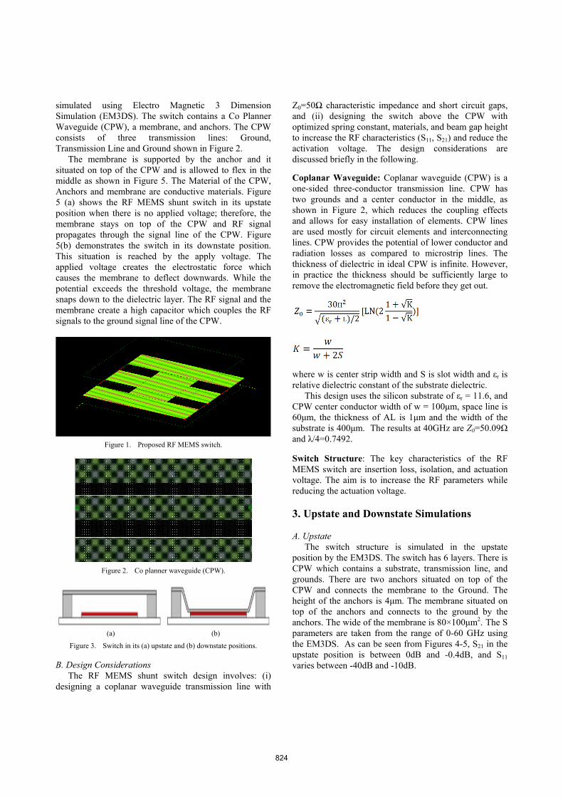
simulated using Electro Magnetic 3 Dimension Simulation (EM3DS). The switch contains a Co Planner Waveguide (CPW), a membrane, and anchors. The CPW consists of three transmission lines: Ground, Transmission Line and Ground shown in Figure 2.
The membrane is supported by the anchor and it situated on top of the CPW and is allowed to flex in the middle as shown in Figure 5. The Material of the CPW, Anchors and membrane are conductive materials. Figure 5 (a) shows the RF MEMS shunt switch in its upstate position when there is no applied voltage; therefore, the membrane stays on top of the CPW and RF signal propagates through the signal line of the CPW. Figure 5(b) demonstrates the switch in its downstate position. This situation is reached by the apply voltage. The applied voltage creates the electrostatic force which causes the membrane to deflect downwards. While the potential exceeds the threshold voltage, the membrane snaps down to the dielectric layer. The RF signal and the membrane create a high capacitor which couples the RF signals to the ground signal line of the CPW.
Figure 1. Proposed RF MEMS switch.
Figure 2. Co planner waveguide (CPW).
(a) (b)
Figure 3. Switch in its (a) upstate and (b) downstate positions.
B. Design Considerations The RF MEMS shunt switch design involves: (i)
designing a coplanar waveguide transmission line with
Z0=50Ω characteristic impedance and short circuit gaps, and (ii) designing the switch above the CPW with optimized spring constant, materials, and beam gap height to increase the RF characteristics (S11, S21) and reduce the activation voltage. The design considerations are discussed briefly in the following.
Coplanar Waveguide: Coplanar waveguide (CPW) is a one-sided three-conductor transmission line. CPW has two grounds and a center conductor in the middle, as shown in Figure 2, which reduces the coupling effects and allows for easy installation of elements. CPW lines are used mostly for circuit elements and interconnecting lines. CPW provides the potential of lower conductor and radiation losses as compared to microstrip lines. The thickness of dielectric in ideal CPW is infinite. However, in practice the thickness should be sufficiently large to remove the electromagnetic field before they get out.
where w is center strip width and S is slot width and εr is relative dielectric constant of the substrate dielectric.
This design uses the silicon substrate of εr = 11.6, and CPW center conductor width of w = 100μm, space line is 60μm, the thickness of AL is 1μm and the width of the substrate is 400μm. The results at 40GHz are Z0=50.09Ω and λ/4=0.7492. Switch Structure: The key characteristics of the RF MEMS switch are insertion loss, isolation, and actuation voltage. The aim is to increase the RF parameters while reducing the actuation voltage. 3. Upstate and Downstate Simulations A. Upstate
The switch structure is simulated in the upstate position by the EM3DS. The switch has 6 layers. There is CPW which contains a substrate, transmission line, and grounds. There are two anchors situated on top of the CPW and connects the membrane to the Ground. The height of the anchors is 4μm. The membrane situated on top of the anchors and connects to the ground by the anchors. The wide of the membrane is 80×100μm2. The S parameters are taken from the range of 0-60 GHz using the EM3DS. As can be seen from Figures 4-5, S21 in the upstate position is between 0dB and -0.4dB, and S11 varies between -40dB and -10dB.
824

Figure 4. S21 in upstate.
Figure 5. S11 in upstate.
B. Downstate The switch in its downstate position does not have
anchors because the membrane should be situated on top of the dielectric layer. Figures 6-7 show that for switch in downstate position the S21 is less than -10dB and S11 is above -1dB for the frequency above the 29GHz.
Figure 6. S21 in downstate.
Figure 7. S11 in downstate.
4. Effects of Varying Geometrical Parameters
In this section, the effects of varying anchor height, membrane size, and dielectric height are studied in upstate and downstate positions. A. Upstate
When the switch is in upstate position, it creates a capacitor between the transmission line and ground. The capacitor should be small so that it does not affect the signal on the transmission line. The S11 and S21 of the scattering parameters illustrate that how this capacitance works on the transmission line.
Tables IV-V show the information about the effects of changing anchor height and membrane size on S11 and S21 of the RF MEMS shunt switch for 2GHz to 50GHz. These parameters are simulated by EM3DS. The RF characteristics of the upstate switch are improved by decreasing the anchor height and the membrane size. The desirable RF characteristics for the RF MEMS switch, while in the upstate position, is for S11 to be below -10dB and S21 above -1dB.
Table IV shows that the S11 and S21 of the RF MEMS switch are below -10dB and above -1dB respectively, while the anchor height is less than 4μm. Decreasing the anchors to 3 and 2μm causes the S11 to become less than -9dB and -7dB respectively.
Table V provides the variation of the size of the membrane, and associated changes in S11 and S21. As it can be seen, for the membrane 40×100μm2, S11 and S21 of this membrane are between -44dB to -14dB and -0.01dB to -0.08dB respectively, for the frequency from 2 to 50GHz. Increasing the size of the membrane causes the S11 and S21 of the switch to decline between -40dB to -10dB and -0.01dB to -0.42dB respectively, for the 80×100μm2. This parameters for the 120×100μm2 is -37dB to -8dB and -0.02dB to -74dB for S11 and S21 respectively.
TABLE IV: EFFECTS OF ANCHOR HEIGHT.
Height S11,2Ghz S11,50Ghz S21,2Ghz S21,50Ghz
6μm -42 -12 -0.01 -0.28
4μm -40 -10 -0.01 -0.42
3μm -39 -9 -0.01 -0.53
2μm -37 -7 -0.01 -0.85
825
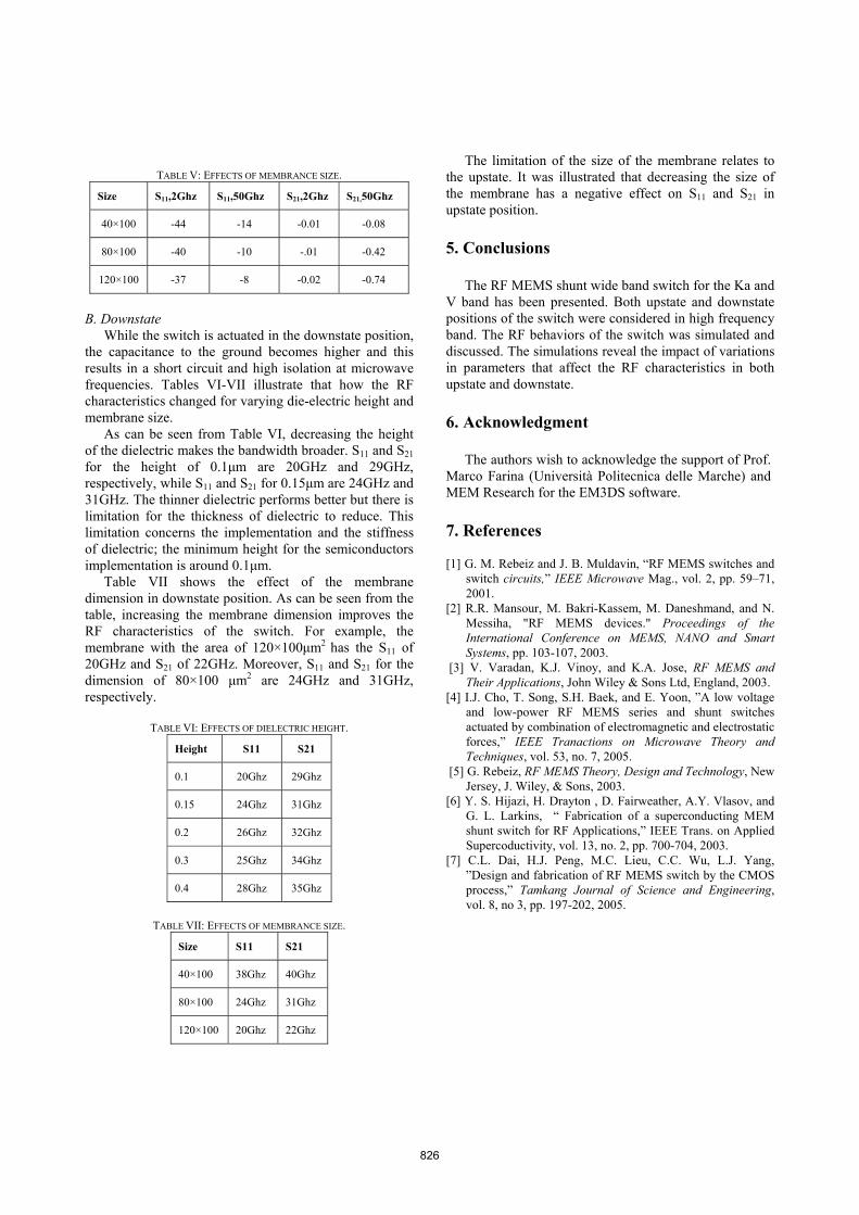
TABLE V: EFFECTS OF MEMBRANCE SIZE.
Size S11,2Ghz S11,50Ghz S21,2Ghz S21,50Ghz
40×100 -44 -14 -0.01 -0.08
80×100 -40 -10 -.01 -0.42
120×100 -37 -8 -0.02 -0.74
B. Downstate
While the switch is actuated in the downstate position, the capacitance to the ground becomes higher and this results in a short circuit and high isolation at microwave frequencies. Tables VI-VII illustrate that how the RF characteristics changed for varying die-electric height and membrane size.
As can be seen from Table VI, decreasing the height of the dielectric makes the bandwidth broader. S11 and S21 for the height of 0.1μm are 20GHz and 29GHz, respectively, while S11 and S21 for 0.15μm are 24GHz and 31GHz. The thinner dielectric performs better but there is limitation for the thickness of dielectric to reduce. This limitation concerns the implementation and the stiffness of dielectric; the minimum height for the semiconductors implementation is around 0.1μm.
Table VII shows the effect of the membrane dimension in downstate position. As can be seen from the table, increasing the membrane dimension improves the RF characteristics of the switch. For example, the membrane with the area of 120×100μm2 has the S11 of 20GHz and S21 of 22GHz. Moreover, S11 and S21 for the dimension of 80×100 μm2 are 24GHz and 31GHz, respectively.
TABLE VI: EFFECTS OF DIELECTRIC HEIGHT.
Height S11 S21
0.1 20Ghz 29Ghz
0.15 24Ghz 31Ghz
0.2 26Ghz 32Ghz
0.3 25Ghz 34Ghz
0.4 28Ghz 35Ghz
TABLE VII: EFFECTS OF MEMBRANCE SIZE.
Size S11 S21
40×100 38Ghz 40Ghz
80×100 24Ghz 31Ghz
120×100 20Ghz 22Ghz
The limitation of the size of the membrane relates to the upstate. It was illustrated that decreasing the size of the membrane has a negative effect on S11 and S21 in upstate position. 5. Conclusions
The RF MEMS shunt wide band switch for the Ka and V band has been presented. Both upstate and downstate positions of the switch were considered in high frequency band. The RF behaviors of the switch was simulated and discussed. The simulations reveal the impact of variations in parameters that affect the RF characteristics in both upstate and downstate. 6. Acknowledgment
The authors wish to acknowledge the support of Prof. Marco Farina (Università Politecnica delle Marche) and MEM Research for the EM3DS software. 7. References [1] G. M. Rebeiz and J. B. Muldavin, “RF MEMS switches and
switch circuits,” IEEE Microwave Mag., vol. 2, pp. 59–71, 2001.
[2] R.R. Mansour, M. Bakri-Kassem, M. Daneshmand, and N. Messiha, "RF MEMS devices." Proceedings of the International Conference on MEMS, NANO and Smart Systems, pp. 103-107, 2003.
[3] V. Varadan, K.J. Vinoy, and K.A. Jose, RF MEMS and Their Applications, John Wiley & Sons Ltd, England, 2003.
[4] I.J. Cho, T. Song, S.H. Baek, and E. Yoon, ”A low voltage and low-power RF MEMS series and shunt switches actuated by combination of electromagnetic and electrostatic forces,” IEEE Tranactions on Microwave Theory and Techniques, vol. 53, no. 7, 2005.
[5] G. Rebeiz, RF MEMS Theory, Design and Technology, New Jersey, J. Wiley, & Sons, 2003.
[6] Y. S. Hijazi, H. Drayton , D. Fairweather, A.Y. Vlasov, and G. L. Larkins, “ Fabrication of a superconducting MEM shunt switch for RF Applications,” IEEE Trans. on Applied Supercoductivity, vol. 13, no. 2, pp. 700-704, 2003.
[7] C.L. Dai, H.J. Peng, M.C. Lieu, C.C. Wu, L.J. Yang, ”Design and fabrication of RF MEMS switch by the CMOS process,” Tamkang Journal of Science and Engineering, vol. 8, no 3, pp. 197-202, 2005.
826