Design and Performance of SMPs With Asynchronous Caches
25
Design and Performance of SMPs With Asynchronous Caches Fong Pong, Michel Dubois*, Ken Lee Computer Systems and Technology Laboratory HP Laboratories Palo Alto HPL-1999-149 November, 1999 E-mail: [email protected] [email protected] [email protected] Asynchronous, cache coherence, shared-memory multiprocessor, SMP We propose and evaluate a cache-coherent symmetric multiprocessor system (SMP) based on asynchronous caches. In a system with asynchronous caches, processors and memory controllers may observe the same coherence request at different points in time. All protocol transactions are uni- directional and processors do not report snoop results. The need for an extensive interlocking protocol between processor nodes and memory controller which is characteristic of snooping buses is thus removed. This design overcomes some of the scalability problem of a multi-drop shared-bus by employing high-speed point-to-point links, whose scalability prospects are much better than for shared buses. Memory and proc essors communicate through a set of queues. This highly pipelined memory system design is a better match to emerging ILP processors than bus-based snooping. Simulation results for ILP processors show that the shared-bus design is limited by its bandwidth. By contrast the parallel link design has ample bandwidth and yields large performance gain for the transaction processing and scientific benchmarks that we have considered. Besides higher performance the asynchronous design we propose considerably simplifies the behavior expected from the hardware. This is important because snooping bus protocols are so complex today that their verification has become a major challenge. * Department of Electrical Engineering-Systems. University of Southern California Los Angeles, California Copyright Hewlett-Packard Company 1999
Transcript of Design and Performance of SMPs With Asynchronous Caches

Design and Performance of SMPs With Asynchronous Caches Fong Pong, Michel Dubois*, Ken Lee Computer Systems and Technology Laboratory HP Laboratories Palo Alto HPL-1999-149 November, 1999 E-mail: [email protected] [email protected] [email protected]
Asynchronous, cache coherence, shared-memory multiprocessor, SMP
We propose and evaluate a cache-coherent symmetric multiprocessor system (SMP) based on asynchronous caches. In a system with asynchronous caches, processors and memory controllers may observe the same coherence request at different points in time. All protocol transactions are uni-directional and processors do not report snoop results. The need for an extensive interlocking protocol between processor nodes and memory controller which is characteristic of snooping buses is thus removed.
This design overcomes some of the scalability problem of a multi-drop shared-bus by employing high-speed point-to-point links, whose scalability prospects are much better than for shared buses. Memory and processors communicate through a set of queues. This highly pipelined memory system design is a better match to emerging ILP processors than bus-based snooping. Simulation results for ILP processors show that the shared-bus design is limited by its bandwidth. By contrast the parallel link design has ample bandwidth and yields large performance gain for the transaction processing and scientific benchmarks that we have considered.
Besides higher performance the asynchronous design we propose considerably simplifies the behavior expected from the hardware. This is important because snooping bus protocols are so complex today that their verification has become a major challenge.
∗ Department of Electrical Engineering-Systems. University of Southern California Los Angeles, California Copyright Hewlett-Packard Company 1999

2
1 Introduction
Because of their simplicity, shared-bus SMPs are a dominant architecture for small-scale systems.
By taking advantage of the broadcast nature of a shared-bus, snooping protocols are the de facto
schemes for achieving cache coherence. Figure 1 shows the basic configuration to support a four-
states MESI protocol [22] which is widely used in cache-coherent shared-memory multiprocessor
systems. In such a system, every processor is associated with a bus watcher (a “snooper”) which
monitors all bus activities. When a processor initiates a coherence transaction such as a load miss
on the bus, all snoopers in all processors latch in the request. These snoop requests consult the
local caches, take necessary actions and respond with appropriate snooping results. Each protocol
transaction on the bus is deemed complete when all caches have reported their snoop result.
Although the snooping bus-based design is a classic, well-understood design and offers many
good features, it is becoming harder to design a shared bus-based SMP that keeps pace with
emerging ILP processor technology.
First and foremost, the multi-drop bus architecture is reaching its speed limit. When the clocking
speed was low, the electrical length of the bus was short enough that distributed behavior of the
bus could be ignored. However, as bus speeds increase, the processor boards connected to the bus
behave as stubs resulting in reflections and ringing of bus signals. There exist several schemes for
terminations and signaling to reduced reflections, but none solves the fundamental problem of
stubs. Because of design constraints such as heat dissipation the space needed between stubs is
longer at high speeds. This limits the operating speed of buses to 150MHz in current systems.
Figure 1 A Bus-based Cache System with Shared/Dirty Signals.
For future processor designs with deep speculation, multiple cores, and/or multithreading [13, 14,
P0
C0
P1 P3
Control+Address
P2bus-watcher
Dirty
C1 C2 C3
Shared

3
23], the shared-bus will no doubt become a major bottleneck even in small multiprocessor config-
urations. An alternative is to have multiple short bus segments bridged by the memory controller
[15, 18]. This approach has its own limitations. It is difficult to connect more than two full busses
to the memory controller without an inordinate number of I/O pins. Furthermore, all bus transac-
tions that occurs in one bus segment must be propagated to other bus segments unless the memory
controller is equipped with coherence filters. A coherence filter essentially keeps track of memory
blocks that are cached in the bus segment. Regardless of these possible extensions, the fundamen-
tal problem of a shared-bus design remains. For instance, every request must start with an arbitra-
tion cycle and spend one cycle for bus turnaround at the end. The protocol sets an upper bound on
the maximum attainable throughput.
Secondly, the bus snooping scheme requires all processors (and all snooping agents such as I/O
bridge chips with I/O caches) to synchronize their responses. Generally speaking, the snoop results
serve three purposes: 1) they indicate the safe completion of the snoop request in the cache hierar-
chy of the local processor, 2) they provide sharing information, and 3) they identify which entity
should respond with the missing data block, i.e, either another processor or memory. For the pur-
pose of illustration (see Figure 1), assume that the snooping results are propagated to all proces-
sors via two bus lines Shared and Dirty. For a load miss, the processor may load the data block into
the exclusive (E) or shared (S) state depending on whether the Shared or Dirty signal is asserted. In
the case where a processor has the most recently modified copy of the requested data, it asserts the
Dirty signal preventing the memory from responding with the data.
Figure 2 Illustration of Snooping Paths in Modern Multiprocessors.
The common approach is to require that all caches connected to the bus generate their snoop
D$ I$
L2$
Concentration
write-back$ prefetching$
L3$
snoop result
4
results in exactly the same bus cycle. This requirement imposes a fixed latency time constraint
between receiving each bus request and producing the snoop result and this fixed snooping delay
must accommodate to the worst possible case. This constraint presents a number of challenges for
the designers of highly-integrated processors with cache hierarchies. As illustrated in Figure 2,
many modules must be snooped and the final results must be concentrated. In order to meet the
fixed latency constraint, the processors may require ultra-fast snooping logic paths. The processor
may have to adopt a priority scheme assigning a higher priority to snoop requests than to requests
from the processor’s execution unit.
More relaxed designs such as Intel’s P6 bus [16] allow processors and memory controllers to insert
wait states when they are slow to respond. This scheme complicates the logic design because
every processor must closely monitor the activities of other processors on the bus in order to re-
generate snooping results when wait states are observed. In the case of Intel’s bus, for instance, the
processor must repeat its snooping result two cycles after observing a wait state cycle.
Yet another approach to synchronizing snoop results is the use of a shared wired-or Inhibit signal
on the bus as was implemented in the SGI Challenge [12]. Processors may snoop at different
speeds but must report the end of their snoop cycle on this new bus line. The transaction remains
“open” for as long as any processor has not pulled down its Inhibit line. Again this interlocking of
processor and memory signals on the bus results in complex bus protocols and bookkeeping of
pending transactions in the interface of each processor, which in fact limits the number of concur-
rent transactions on the bus. The design still relies on a shared line and on bus watching and is
complex to verify. This complexity increases with the number of concurrent transaction tolerated
on the bus. Current designs are so complex that verification has become a major development cost.
In this paper, we propose an efficient cache-coherent shared-memory multiprocessor system based
on an asynchronous-snooping scheme. In this paper asynchronous refers to a model of cache-
coherent systems first theoretically introduced and proven correct in [2]. It does not refer to vari-
able-delay snooping using an inhibit line as described above. In fact it does not require reporting
snoop results or synchronizing the snoops in any way. Because of this simplification, fast, high-
bandwidth point-to-point links can be used to communicate requests and data between processors
and memory. Snooping requests to different processors are propagated independently through
queues. The number of pending and concurrent protocol transactions is only limited by the size of

5
these FIFO queues. However by emulating a shared-bus broadcast protocol, the topology of the
point-to-point interconnection is made transparent to the processors and the memory.
The various design aspects of the new system are given in Sections 2 and 3. Section 4 is dedicated
to the evaluation methodology and system simulation models. We compare the effectiveness of
various bus-based configurations with our parallel link design. These results are presented and dis-
cussed in Section 5 and our final comments conclude the paper in Section 6.
2 A New Asynchronous Cache System Design
2.1 The Architectural Organization
We advocate an asynchronous cache system such as the one shown in Figure 3. In this design, pro-
cessors and memory controller communicate via unidirectional high-speed links [10, 25]. A set of
queues buffer requests and data blocks in case of access conflicts and also serve as adaptor
between data paths of different width.
Figure 3 The Proposed Asynchronous Cache System.
On the memory controller side, received requests are stored in a request queue. Through a high-
state data
state data blocks
bank0
state data
state data
bank1
{
Mem
Q
memory controller
Snoo
pQ
parallel links
D$
address bus
I$
L2$
Scheduling Window/
data bus
Dat
aQ
Req
Q
bank2 bank3
processor 0
D$ I$
L2$
processor 1
p2 p3
Req
uest
Dat
a
Memory Disambiguation
Incoming Buffer

6
speed address bus internal to the memory controller, requests are routed to the snoop queues of all
processors. Emerging from the snoop queue, request packets are transmitted through the links to
the incoming buffers of processors. When they reach their destination, packets may snoop various
caches in the node and a data response may be generated as a point-to-point packet to the request-
ing processor through a data bus internal to the memory controller chip.
Note that the on-chip address and data busses may be both implemented by a multiplexer to data
lines feeding into all processors incoming queues. Speed of this path can be made very fast,
depending on the distance and the RC delay of the process technology.
2.2 Memory Disambiguation and Access Ordering
All the queues in this design are FIFOs (First-In-First-Out). In term of ordering of memory
accesses, the behavior of this system has been shown to be indistinguishable from a platform with
a shared bus [2, 19]. The address bus internal to the memory controller serves as a global ordering
point for all memory accesses.
For correctness, there are certain rules the system must support:
1. The processor keeps track of all pending instructions in the scheduling window or the memory
disambiguation buffer. Instructions are retired in program order.
2. Loads that are executed, but have yet to retire from the memory disambiguation buffer are sub-
ject to snooping requests. A write-invalidation arriving before retiring the load will cause the
load to be re-issued and all instructions depending on the load to be re-played.
3. Values of stores are written to the cache/memory system only when they are retired from the
scheduling window, although the fetch of an exclusive cache line can proceed speculatively.
Specifically, when a store operation is inserted into the scheduling window, a speculative access
may be issued to the cache system to obtaining a local writable copy of the block. However, the
store is actually executed only when it emerges at the head of the scheduling window.
4. When the memory controller receives a request, the request is routed via the internal address
bus to the input snoop queues of all processors, including the processor that made the
request. At this point, a global ordering point has been established so that all processors
observe the same sequence of events.
5. Before processor pi can retire a request from its incoming snoop buffer, all requests received

7
before it in the buffer must have been completed.
It is really not difficult to comprehend that a total order on all stores can be constructed in this sys-
tem and that all the stores can only be observed in that order by any processor. Thus the system is
sequentially consistent, the strongest form of memory consistency.
2.3 The Cache Protocol
Because we have no Shared, Dirty or Inhibit bus lines, we need to adapt parts of the protocol that
rely on such lines. First, we cannot implement the E (Exclusive) state of the MESI protocol. This is
easily done by using a simpler, MSI protocol. Second we need to make sure that one and only one
cache or memory responds with the data on a cache miss. A classical solution to this problem is to
maintain one Valid bit per block in memory. A memory block can be in one of two states: memory-
invalid (MI) and memory-valid (MV). If a memory block is in the MI state, one of the processors
must have a modified copy and supply the copy on a miss. If a memory block is in the MV state,
some processor caches may have a shared block that must be consistent with the memory copy and
the memory delivers the copy. Because of this valid bit processors or memory controller do not
need to report who provides a data copy. Third the inhibit line or the fixed latency snoop delay
become useless because the protocol is now asynchronous and does not rely on the broadcasting
snoop results.
The protocol uses only MSI states, which is a derivation from the MESI protocol. By definition, we
have:
1. Modified (M). When a cache is in the modified state, it has the most recent copy. This cache is
also responsible for responding to a subsequent miss. The memory state must be invalid (MI).
2. Shared (S). The block may be shared among processors. The memory copy is valid (MV) and
the memory is to respond to a subsequent miss.
3. Invalid (I). The cache does not have the memory block.
The protocol works as follows:

8
1. Read miss. If another cache has a modified copy, it responds to the requesting cache with a data
copy, and updates the main memory as well. Otherwise, the memory must have a valid copy
which is directly supplied to the requesting cache. At the end, all cached copies are in the
shared state, and the memory is in the memory-valid state.
2. Write hit. If the block is in the modified state, the write can proceed without delay. Otherwise,
the cache block is always re-loaded, as in a write miss1.
3. Write miss. A write miss request is sent to the memory and to all other processors. If the mem-
ory has a valid copy, the memory will provide its copy to the requesting processor. Otherwise,
the current owner will respond to the request. At the end, the requesting processor will load the
block in the modified state. All other processors with a valid block set their state to invalid. The
memory state is set to memory-invalid so that the memory will ignore subsequent misses.
2.4 Self-Regulation and Credit-Based Flow Control
In the asynchronous cache system, the number of pending protocol transactions is only limited by
the finite sizes of the queues. To avoid overflow of the request and data buffers a simple credit-
based flow control scheme will do. Each processor limits the number of its outstanding requests to
n. As shown in Figure 3, each processor has its own dedicated buffer at the memory controller and
thus each buffer must hold n entries at the memory controller. Initially, the processor has n credits.
The processor decreases its credits by one when a new request is sent and increases its credits by
one when a reply is propagated back from the memory controller.
The memory controller may also inform the processor on the amount of available buffer space in
its incoming request and data buffers. For instance, when the memory controller propagates a
snoop request to processor pi, it may piggyback the number of available entries for pi’s out-bound
data buffers with the request.
In the asynchronous design, flow control is achieved by self-regulation without overhead. By con-
trast, in the pipelined shared-bus design, processors and memory controller must arbitrate for the
memory bus when they want to send requests. For data transfer, the sender must listen to the ready
1. This is done to simplify the protocol. However, the protocol would be more efficient and consume less interconnectbandwidth if the processor issued an Upgrade request instead [9]

9
signal from the receiver, and wait until the data bus is freed by a prior transfer.
To illustrate the complexity introduced by the shared-bus interface design consider the case of
back-to-back requests issued to the bus for the same memory block shown in Figure 4.
Figure 4 Race Condition for Back-to-Back Requests in a Shared-bus System.
In this example, every processor receives two back-to-back requests to the same memory block, in
cycle 1 and in cycle 3. For the first request, the processor looks up its cache in cycle 2, computes a
new state in cycle 3, and then installs the new state in cycle 4. Unfortunately, the snooping result
of the second request depends on the new state computed after the first request, which will be only
available after cycle 4. The situation is even more complex from the point of view of the processor
issuing the first request. This processor may receive the second request before it even knows if its
own request will complete, be deferred or be retried [16]. This is why concurrent requests to the
same block are often disallowed in split-transaction bus systems. In the proposed asynchronous
design, all these problems are solved without undue complexity by respecting the FIFO order of
all requests and responses throughout the memory system. The asynchronous protocol does not
check for nor constraint the number of concurrent transactions to the same block.
2.5 Trade-offs Made in the Proposed Design
2.5.1 Elimination of the Exclusive State
Traditionally, the exclusive (E) state has been advocated to reduce the consumption of bus band-
width when a load miss is followed by a store hit to the same cache line. This is because store
accesses to cache lines in the E state are resolved locally in the processor without incurring bus
accesses.
snoop&latch
snoop_result
snoop&latch
lookup
addr1
addr2=addr1
Cycle 1 Cycle 2 Cycle 3 Cycle 4 Cycle 5
lookup
compute
install newstate

10
Since processors do not report sharing status in our proposed design, the exclusive state cannot be
supported, at least in a simple way. The minimum cost of not having the exclusive state, is the
additional bus bandwidth required to propagate an Upgrade request (one control packet) on the bus
on the first write following a read miss. Since our design accommodates a much larger bandwidth
than current bus designs and is highly pipelined, the absence of an exclusive state is not a problem.
Even in the context of bus-based systems, the absence of the exclusive state create negligible addi-
tional bandwidth consumption in parallel and multiprogrammed workloads as is shown in [9]
when Upgrades are used. In our MSI protocol, the absence of an exclusive state is more costly
because we take a miss on every write hit to a Shared copy (see Section 2.3) in order to simplify
the protocol.
In the future, we can expect that the exclusive state may become totally useless if hardware and/or
compiler can detect migratory sharing in parallel workloads [7, 21] and accesses to private data in
multiprogrammed workloads and give hints to the cache on load misses. In section 5, we will show
the impact of dropping the exclusive state on system performance.
2.5.2 Increased Memory Bandwidth Consumption
Another potential drawback of the proposed design is that it may require more memory bandwidth
support because, if the valid bit in each memory block is stored in the same DRAM as the data, the
valid bit in memory must be always consulted and sometimes updated on every main memory
access.
By contrast, traditional shared-bus design may allow a memory access to be squashed to save
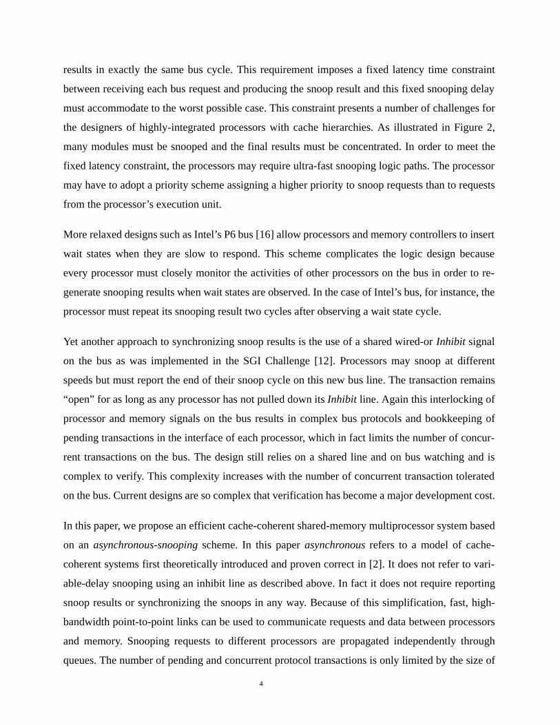
memory bandwidth whenever a processor replies. As shown in Figure 5, when the processors
probe their local caches on snoop requests, the memory controller normally starts a “speculative”
access in parallel in order to reduce latency in case no processor owns the requested block. This
memory access is termed “speculative” because it proceeds without knowing whether the data
copy from memory will be used. With a proper design, “speculative” memory accesses may be
dequeued from the memory queues when one of the processors asserts the Dirty line on the bus. It
is, however, important to note that in many cases the memory access may still be unavoidable:
Since the “speculative” access may start as early as the address is known, the snoop result may
arrive too late to cancel the access. As a result, the speculative access may still have to complete,
11
but the memory does not return the copy.
Figure 5 Speculative Memory Access by the Memory Controller in Snooping Protocols.
Another problem is that the valid bit must at times be updated, which requires another DRAM
access in some cases.
A radical solution to these problems would be to store the valid bits in a separate, fast SRAM chip,
which is accessed in parallel with the memory. However our results show that, for our bench-
marks, bus-based snooping protocols are not really able to save much memory bandwidth by can-
celling DRAM block accesses.
The idea of a valid bit associated with each memory block is not new. In the Synapse protocol
[11], when the cache with a modified line does not respond fast enough to a miss, the valid bit
inhibits the memory from responding. This idea was also adopted in [3] in the design of a snoop-
ing protocol for unidirectional slotted rings. In this design a snoop request propagates from node to
node and the memory state must be snooped together with the cache state because a snoop request
visits each node only once.
3 Advances in Serial-Links Technology
The performance of high-speed CMOS serial links is growing rapidly [10, 25]. These links are
suitable for point-to-point connection in impedance controlled environment. The reflection prob-
lems plaguing multi-drop bus are eliminated. Data rates up to 4Gbit/sec have been demonstrated
using conventional CMOS technology.
It is still premature to consider these technologies in massively parallel implementations because
of their power, area, latency, and error rate characteristics. However, with the advances in CMOS
P0 puts request and address on the control bus
P1 latches in the request A
Pn latches in the request
local cache lookup
if the Dirty signal is asserted, thefetched memory block is droppedspeculative memory accessMemory controller
A
A
A
local cache lookup
Clock
latches in the request

12
technology and circuit implementation, it is conceivable that differential 4Gbit/sec links will
become available in the near future. The chip area needed by each link is basically the I/O pad area
and power consumption is sufficiently low that hundreds of these links could be implemented on a
single chip. The latency could be as small as 2-3 cycles plus time of flight.
The following performance evaluations of the proposed asynchronous cache system have been
carried out assuming links with bandwidths of 1 and 2 Gbit/sec.
4 Methodology for Performance Evaluation
The primary goal of this study is to provide some quantitative comparison of the proposed asyn-
chronous protocol design with typical bus-based designs. We use cycle-accurate, trace-driven sim-
ulation models for both the asynchronous design and traditional bus-based SMPs. Both models are
described below in some details.
4.1 Workloads
In this study, we use an Oracle, TPC-C trace which was collected on a 4-way HP server by a tool
based on object-code-translation technology [1]. The tool instruments the code to dump memory
traces. In this configuration, the TPC-C traces are composed of trace files for 22 processes. These
processes are partitioned and scheduled on the four processors in a dedicated manner. The traces
contains user-space accesses only. We also use three benchmarks from the SPLASH2 suite [24].
Table 1 lists the footprints and number of instruction fetches, loads and stores in each benchmark.
4.2 Simulation Model
4.2.1 The Asynchronous Cache Model
The asynchronous caching model is shown in Figure 3. We simulate a 4-way SMP node. Every
Table 1 Characterization of Workloads.
BenchmarksCode Space Footprint Data-set Size
Num. of Instructions Num. of Loads Num. of Stores
TPCC 2MB 15MB 200,000,000 47,278,610 26,462,984
FFT 4KB 3MB 36,709,821 4,964,999 2,868,340
RADIX 4KB 8MB 101,397,013 41,039,729 9,544,862
OCEAN 45KB 15MB 292,565,301 77,345,166 18,326,143

13
processor has a 128KB, level-1 write-through data cache, a 128KB, level-1 instruction cache and a
1MB level-2 write-back cache. All caches are 4-way set-associative and lockup-free.
The Processor Model
We approximate an processor core which enables out-of-order issuances and in-order completions
of memory accesses. It is an approximation because information of data dependency is not avail-
able in our traces. The traces contain all instructions. Instructions are inserted one by one in a 96-
entry buffer and are retired one by one. Loads and stores can retire at the head of the buffer if they
do not access a pending block in the second level caches. Instruction accesses are also simulated.
The histogram of the number of pending instructions, loads and stores misses at the time when a
new second-level cache miss is issued is displayed in Figure 6. In most cases there are no or few
pending misses. The figure shows that the average number of pending misses is quite reasonable
and that the absence of dependency information in the trace does not unduly stress the memory
system.
Figure 6 The Number of Pending Misses When Issuing a New Miss.
Furthermore, in the SPLASH2 benchmarks, most data elements are accessed by indexing into data
arrays within loops. For instance, one code line may read as:
dest[n+m]= x[i*k] +x[i*k+1]
where n, m, i, k are typically private variables of processes that control the loop. The computation

14
of the indices should not cause global coherence traffic and should hit in the cache. As a result, the
danger of issuing the loads to data array x much too early is limited. The only problem is the store
to the dest data array. In this case, our approximation tends to aggressively prefetch the destination
data block based on addresses. Nevertheless, we believe the number of pending accesses as shown
in Figure 6 is reasonable, in particular for future processors with deep speculative execution.
The Memory Subsystem
A cache miss injects a request into the processor’s outgoing request queue. The request packet is
128 bits long. The request packet is then muxed out through the parallel links (1gbps or 2gbps),
entering the request queue (ReqQ) of the memory controller. Subsequently, the request is routed to
the snoop queues of all processors as well as to the memory queue via an 128-bits wide internal
bus. Finally, data blocks are routed through a separate 256-bits wide internal data bus in the model.
Figure 7 Basic Timing for a Read Burst.
There are four memory banks. The memory devices are 100MHz SDRAMs2 with four internal
banks [20]. For these devices, a memory access starts with an ACTIVE command. A READ/
WRITE command is given after tRCD. For a READ, the first bit of data is available after a read
latency tCAS; for a write, the data is driven on the inputs at the same cycle where the WRITE
command is given. Figure 7 shows the basic timings.
It is important to note that a subsequent ACTIVE command to a different row in the same internal
2. The experiment can be extended to other types of DRAMs such as DDR-SDRAM and DRDRAM. We choose thesimple SDRAMs to study memory bandwidth issues. The simulated system supports a data bandwidth of 6.4GB/s. Itis a reasonable configuration for today’s design.
Active
Clock
Read
tRCD tCAS
tRRD
D0 D1 D2 D3
tRC
15
bank can only be issued after the previous active row is closed. Therefore, the minimum time
interval between successive accesses to the same internal bank is defined by tRC. On the other
hand, a subsequent ACTIVE command to another internal bank can be issued when the first bank
is being accessed. The minimum time interval between successive ACTIVE commands to differ-
ent banks is defined by tRRD. In our simulation, we model the DRAM modules accordingly.
However, we do not model an optimal memory controller design that may schedule accesses to
interleaved banks in order to maximize throughput.
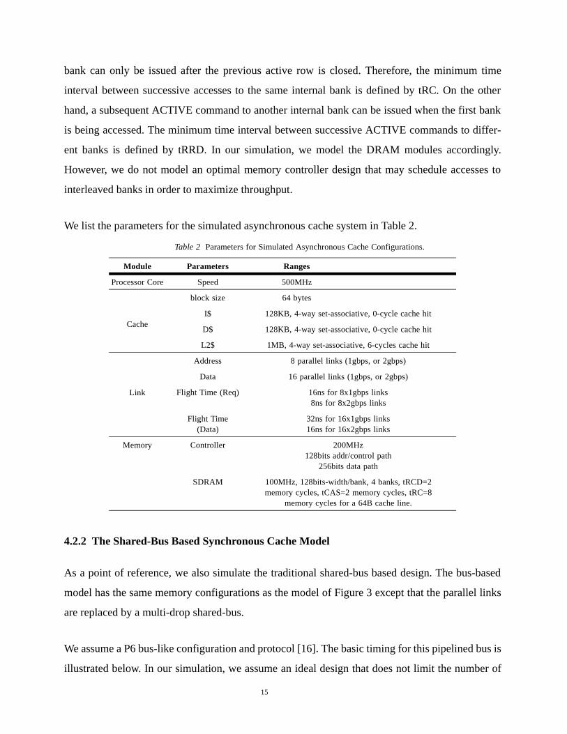
We list the parameters for the simulated asynchronous cache system in Table 2.
4.2.2 The Shared-Bus Based Synchronous Cache Model
As a point of reference, we also simulate the traditional shared-bus based design. The bus-based
model has the same memory configurations as the model of Figure 3 except that the parallel links
are replaced by a multi-drop shared-bus.
We assume a P6 bus-like configuration and protocol [16]. The basic timing for this pipelined bus is
illustrated below. In our simulation, we assume an ideal design that does not limit the number of
Table 2 Parameters for Simulated Asynchronous Cache Configurations.
Module Parameters Ranges
Processor Core Speed 500MHz
block size 64 bytes
CacheI$ 128KB, 4-way set-associative, 0-cycle cache hit
D$ 128KB, 4-way set-associative, 0-cycle cache hit
L2$ 1MB, 4-way set-associative, 6-cycles cache hit
Link
Address 8 parallel links (1gbps, or 2gbps)
Data 16 parallel links (1gbps, or 2gbps)
Flight Time (Req) 16ns for 8x1gbps links8ns for 8x2gbps links
Flight Time (Data)
32ns for 16x1gbps links16ns for 16x2gbps links
Memory Controller 200MHz128bits addr/control path
256bits data path
SDRAM 100MHz, 128bits-width/bank, 4 banks, tRCD=2 memory cycles, tCAS=2 memory cycles, tRC=8
memory cycles for a 64B cache line.

16
concurrent bus transactions.
Figure 8 Pipelined Bus Transactions.
In general, a transaction starts with an arbitration cycle, followed by two request cycles. The snoop
result is reported at the 4th cycle after the first request phase. Finally, the data phase starts at the
6th cycle after the first request cycle. As clearly shown in the timing diagram of Figure 8, the max-
imum request rate to the bus is one request every three bus cycles. Furthermore, the data phase
may incur a long queueing delay for data returns.
Table 3 summarizes the parameters for our simulations of bus-based systems.
5 Performance Evaluation Results
5.1 Cache Misses
Table 4 lists the percentages of types of L2 cache accesses. Since most instruction fetches and
Table 3 Parameters for Simulated Shared-Bus Configurations.
Module Parameters Ranges
Processor Core Speed 500MHz
block size 64 bytes
CacheI$ 128KB, 4-way set-associative, 0-cycle cache hit
D$ 128KB, 4-way set-associative, 0-cycle cache hit
L2$ 1MB, 4-way set-associative, 6-cycles cache hit
Busclock 100MHz
Data 64-bits data bus, 8 bus cycles for 64B cache line
Data (double-pumped) 64-bits data bus, 4 bus cycles for 64B cache line
Data(double-pumped) 128-bits data bus, 2 bus cycles for 64B cache line
Memory SDRAM 100MHz, 128bits-width/bank, 4 banks, tRCD=2 memory cycles, tCAS=2 memory cycles, tRC=8
memory cycles for a 64B cache line.
Arb Req Req Err Err SNP RSP D0 D1 D2 D3 D4 D5 D6 D7
Arb Req Req Err Err SNP RSP D0
Arb Req Req Err Err SNP RSP D0 D1 D2 D3 D4 D5 D6 D7
Arb Req Req Err Err SNP RSP D0
Arb Req Req Err Err SNP RSP D0

17
loads hit in the L1 caches, stores accesses count for most of L2 cache accesses. Given a 1MB L2
cache, the miss rates are reasonably small.
From Table 4, one can see that the stores to cache lines in the exclusive state represent a very small
percentage of all accesses to the second level cache. In [17], Keeton reported a similar result and
suggested that the E state is not very useful for OLTP applications. However, when we remove the
E state as we did in the proposed asynchronous design, the net result is that the number of L2
cache misses increases by about 18% for TPC-C and OCEAN, whereas it is negligible for the
other benchmarks. This comes from the fact that in our protocol we take a miss on every write to a
shared copy.
This drastic miss rate increase may have a profound impact on overall system performance, espe-
cially when the processor is clocked at very fast speeds and/or the hit rate of the cache system is
high. A system with the MSI protocol used in this paper must resolve cache misses quicker in
order to compensate for the higher number of cache misses. In a system with ILP processors, this
means that the memory system must support greater bandwidth such that contention for shared
resources such as the system bus is reduced.
5.2 Total Execution Time and Average Latency Per Cache Miss
Figure 9 shows the total execution times. All runs are normalized to the baseline shared-bus archi-
tecture with a simple 64-bits data bus that takes 8 cycles to transfer a 64B data block. The second
and the third columns show the results of shared-bus designs with data bus bandwidths two and
four times that of the baseline system. The fourth and the fifth columns correspond to the proposed
Table 4 Characterization of L2 Cache Accesses (MESI Protocol).
Applications Read Hits Read Miss Write Miss Write to Shared Write to Exclusive Write to Modified
TPC-C 6.82% 1.88% 0.50% 0.18% 0.44% 90.18%
FFT 1.2% 2.14% 1.15% 0.41% 0.12% 94.98%
RADIX 0.41% 3.67% 2.10% 0.06% 0.06% 93.70%
OCEAN 14.97% 4.25% 3.78% 0.26% 1.94% 74.80%
18
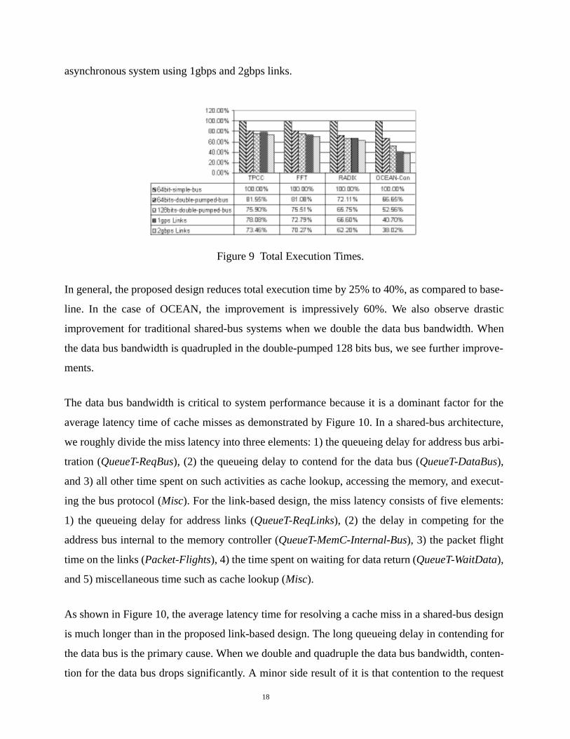
asynchronous system using 1gbps and 2gbps links.
Figure 9 Total Execution Times.
In general, the proposed design reduces total execution time by 25% to 40%, as compared to base-
line. In the case of OCEAN, the improvement is impressively 60%. We also observe drastic
improvement for traditional shared-bus systems when we double the data bus bandwidth. When
the data bus bandwidth is quadrupled in the double-pumped 128 bits bus, we see further improve-
ments.
The data bus bandwidth is critical to system performance because it is a dominant factor for the
average latency time of cache misses as demonstrated by Figure 10. In a shared-bus architecture,
we roughly divide the miss latency into three elements: 1) the queueing delay for address bus arbi-
tration (QueueT-ReqBus), (2) the queueing delay to contend for the data bus (QueueT-DataBus),
and 3) all other time spent on such activities as cache lookup, accessing the memory, and execut-
ing the bus protocol (Misc). For the link-based design, the miss latency consists of five elements:
1) the queueing delay for address links (QueueT-ReqLinks), (2) the delay in competing for the
address bus internal to the memory controller (QueueT-MemC-Internal-Bus), 3) the packet flight
time on the links (Packet-Flights), 4) the time spent on waiting for data return (QueueT-WaitData),
and 5) miscellaneous time such as cache lookup (Misc).
As shown in Figure 10, the average latency time for resolving a cache miss in a shared-bus design
is much longer than in the proposed link-based design. The long queueing delay in contending for
the data bus is the primary cause. When we double and quadruple the data bus bandwidth, conten-
tion for the data bus drops significantly. A minor side result of it is that contention to the request

19
bus may increase slightly. This is because the processors can resolve misses quicker and, conse-
quently, issue accesses quicker.
Figure 10 Average Latency for a Cache Miss.
When we quadruple the data bus bandwidth (double-pumped 128-bits wide bus), the average
latency time of a cache miss is about the same as for the asynchronous system based on 1 gbps
links. Recall that, as we have shown in section 5.1, the number of cache misses for the asynchro-
nous design using the MSI protocol is higher than for the baseline shared-bus system using the
MESI protocol. As a result, we have observed that the shared-bus design with a 128-bits wide dou-
ble-pumped data bus performs slightly better than the 1gbps link-based system for TPC-C and
RADIX as shown in Figure 9.
Figure 11 The Data Bus Occupancy.
For OCEAN, the data bus is simply overwhelmed due to higher cache miss rate and heavy write-
back traffics. Figure 11 shows random snapshots of data bus occupancy. It is clear that the data bus
traffic is constantly high for OCEAN. On the other hand, the proposed linked-based design can
TPC-C FFT RADIX OCEAN
OCEAN
RADIX
FFT
TPC-C
Time Window
20
accommodate this high traffic. Because every processor to memory data path supports 2GB/s
(4GB/s) of bandwidth with 16x1gbps (16x2gbps) links. The total aggregate bandwidth is 8GB/s
(16GB/s), which is much higher than the data bus bandwidth (3.2GB/s for a double-pumped 128-
bits bus).
Figure 10 also shows that the average miss latency in the link-based design is dominated by the
time waiting for data returned from the memory system. In our simulations, we consider a conser-
vative design in which the memory controller fetches the entire data block before it attempts to
stream the data down the links. Therefore, from the point in time when the memory bank control-
ler receives the request, it will take about 70ns to fetch a block, and an additional 30-to-40ns to
return the packet. We also observe that the contention delays for memory banks are around 14ns,
18ns, 6ns and 72ns for TPC-C, FFT, RADIX and OCEAN. It is very important to realize that the
proposed asynchronous design still has room for performance improvement. For instance, by add-
ing small on-chip caches by the side of memory bank controllers, the memory access time and
bank contention can be cut down significant if the hit rates are high.
5.3 Memory System Performance
In this section, we investigate issues related to the memory system performance. For shared-bus
based systems, an important criteria is how effective the snooping protocol is at reducing memory
bandwidth consumption. Recall that the memory controller usually starts a “speculative” access in
parallel with the processor cache lookup operation (Figure 5). Ideally, a speculative memory
access should be squashed before it is scheduled to access the memory data array. This means that
the snooping results should be delivered in time.
Table 5 shows the percentage of memory accesses that are cancelled in time and the percentage of
memory accesses that are useless in the bus-based snooping protocol. The second and the third
columns of Table 5 show percentages with respect to the numbers of loads and stores accessing
memory blocks cached in the modified state by other processors, whereas the fourth and fifth col-
umns show percentages with respect to all accesses. The reason to show both percentage numbers
is that, when a load or a store accesses a valid memory block, the memory access is needed. As a
result, we are more interested in the effectiveness of the snooping bus to prevent memory accesses
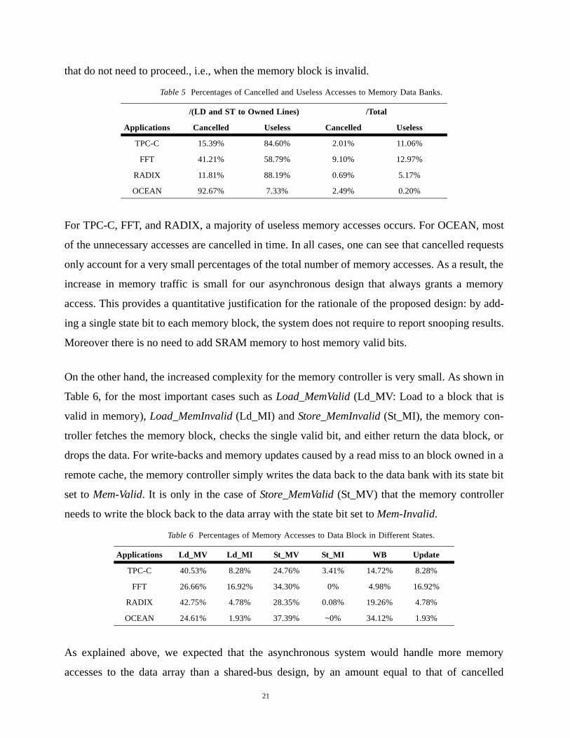
21
that do not need to proceed., i.e., when the memory block is invalid.
For TPC-C, FFT, and RADIX, a majority of useless memory accesses occurs. For OCEAN, most
of the unnecessary accesses are cancelled in time. In all cases, one can see that cancelled requests
only account for a very small percentages of the total number of memory accesses. As a result, the
increase in memory traffic is small for our asynchronous design that always grants a memory
access. This provides a quantitative justification for the rationale of the proposed design: by add-
ing a single state bit to each memory block, the system does not require to report snooping results.
Moreover there is no need to add SRAM memory to host memory valid bits.
On the other hand, the increased complexity for the memory controller is very small. As shown in
Table 6, for the most important cases such as Load_MemValid (Ld_MV: Load to a block that is
valid in memory), Load_MemInvalid (Ld_MI) and Store_MemInvalid (St_MI), the memory con-
troller fetches the memory block, checks the single valid bit, and either return the data block, or
drops the data. For write-backs and memory updates caused by a read miss to an block owned in a
remote cache, the memory controller simply writes the data back to the data bank with its state bit
set to Mem-Valid. It is only in the case of Store_MemValid (St_MV) that the memory controller
needs to write the block back to the data array with the state bit set to Mem-Invalid.
As explained above, we expected that the asynchronous system would handle more memory
accesses to the data array than a shared-bus design, by an amount equal to that of cancelled
Table 5 Percentages of Cancelled and Useless Accesses to Memory Data Banks.
/(LD and ST to Owned Lines) /Total
Applications Cancelled Useless Cancelled Useless
TPC-C 15.39% 84.60% 2.01% 11.06%
FFT 41.21% 58.79% 9.10% 12.97%
RADIX 11.81% 88.19% 0.69% 5.17%
OCEAN 92.67% 7.33% 2.49% 0.20%
Table 6 Percentages of Memory Accesses to Data Block in Different States.
Applications Ld_MV Ld_MI St_MV St_MI WB Update
TPC-C 40.53% 8.28% 24.76% 3.41% 14.72% 8.28%
FFT 26.66% 16.92% 34.30% 0% 4.98% 16.92%
RADIX 42.75% 4.78% 28.35% 0.08% 19.26% 4.78%
OCEAN 24.61% 1.93% 37.39% ~0% 34.12% 1.93%

22
requests in Table 5. However, in our simulations, we actually observed 15.56%, 30.45%, 19.95%,
and 38.44% increases for TPC-C, FFT-RADIX and OCEAN, respectively. This is due to our
choice of the MSI protocol in which processors always re-load the data block when a write hits a
cache line in the shared state. If one optimizes the cache protocol such that writes hitting shared
lines simply request an upgrade from memory, one may see some performance improvements.
6 Conclusion and Future Research
The SMP architecture model is a predominant design style for small scale systems. However, the
traditional shared-bus based design is quickly approaching its scalability limitations. In [8], it was
shown that small-scale SMPs are limited by the bandwidth of the data bus. For medium or large
systems, the system performance is limited by the snooping rate of the bus. On the other hand, the
memory system bandwidth is not a limiting factor. Based on technology trends, future processors
will support more parallelism by supporting deep speculation or multiple cores. As a result, a
future small-scale SMP may have an equivalent level of demand for both snoop and data band-
width as today’s medium systems. The mature shared-bus design is not a viable solution for the
future.
Generally speaking, the data bandwidth problem can be solved by using high-bandwidth data
switches. However, for small scale systems, a bus-like interconnect is still a better solution
because of the latency overhead involved in routing data through switches [8]. Observing the rapid
improvement of parallel-link technology, we have proposed and evaluated a specific implementa-
tion of SMPs with a deeply pipelined memory system designed with parallel-link interconnection
and queues, which is a better match for future ILP processors. The parallel-link topology is trans-
parent to software since the proposed architecture uses a bus-like broadcast protocol.
Our results are consistent with Keeton [17] in that writes to cache lines in the exclusive state are a
very small percentage of the total number of accesses. However, if we compare the frequency of
these events with respect to cache misses, they can be a significant portion. Thus, we observed that
the number of cache misses may increase significantly when the exclusive state is not supported.
Since the system performance is eventually determined by the processor idle time, it may become
more important than ever to reduce the number of cache misses when the speed gap between pro-
cessor and memory keeps increasing. It would be interesting to study how much performance

23
improvement can be further achieved in the proposed asynchronous system design by incorporat-
ing the exclusive state.
As expected, the memory bandwidth requirement of the proposed design is higher by about 20 to
30 percents over traditional bus-based designs. A large portion of the bandwidth increase is due to
the fact that we systematically and deliberately pursed design simplicity. Simplicity is becoming
more and more important because of the cost of verifying the behavior of current very complex
designs. Nevertheless, we do find this extra bandwidth demand does not cause much contention
problem at the memory banks.
Given high-bandwidth links, we found that the latency for accessing the memory banks is the pri-
mary component of the overall cache miss latency. This problem can be solved by caching mem-
ory blocks at the memory controller in a shared cache. It would be interesting to understand how
big a shared cache is needed next to each memory bank controller in order to absorb the extra traf-
fic.
Finally, we envision that a reasonably large-scale system can be implemented by using the pro-
posed design as a building block. There are many possibilities. For instance, one can imagine add-
ing another level of point-to-point interconnects to form a hierarchical bus-like topology.

24
Reference
[1] Abandah, G.A., Davidson, E.S., “Configuration Independent Analysis for Characterizing
Shared-Memory Applications”, Proc. of the 12th Int’l Parallel Processing Symposium, March
1998.
[2] Afek, Y., Brown, G. and Merritt, M., “Lazy Caching", ACM Transactions on Programming
Languages and Systems, vol. 15 , issue 1 (1993) , pp. 182-205.
[3] Barroso, L., and Dubois, M., “The Performance of Cache-Coherent Ring-based Multiproces-
sors,” Proc. of the 20th Annual International Symposium on Computer Architecture, pp. 268-
277, 1993.
[4] Bilir, E.E., Dickson, R.M. Hu, Y., Plakal, M., Sorin, D.J., Hill, M.D., and Wood, D.A., “Mul-
ticast Snooping: A New Coherence Method Using a Multicast Address Network”, Proc. of the
International Symposium on Computer Architecture, 1999.
[5] Borrill, P. L., “Why Open, and Why Buses”, Proc. of Open Bus System, pp. 25-31, 1991.
[6] Brown, G., "Asynchronous MultiCaches", Distributed Computing, vol. 4, pp. 31-36, 1990.
[7] Cox, A.L. and Fowler, R. J., “Adaptive Cache Coherency for Detecting Migratory Shared
Data”, Proc. of the 20th Annual International Symposium on Computer Architecture, pp. 98-
108, 1993.
[8] Charlesworth, A., “Starfire: Extending the SMP Envelope”, IEEE Micro, Jan./Feb. 1998, pp.
39-49.
[9] Culler, D.A. and Singh, J.P., “Parallel Computer Architecture: A Hardware/Software
Approach. Morgan-Kaufmann Publishers, San Francisco, California, 1999.
[10] Dally, W.J. and Poulton, J., "Transmitter equalization for 4Gb/s signalling", Proc. Hot Inter-
connects Symp., pp.29-39, Aug. 1996, pp.29-39.
[11] Frank, S. J., “Tightly Coupled Multiprocessor Systems Speed memory Access Times”, Elec-
tronics, 57, 1, pp. 164-169, 1984.
[12] Galles, M. and Williams, E., “Performance Optimizations, Implementation, and Verification
of the SGI Challenge Multiprocessor,” Proc. of the 27th Hawaii International Symposium on
System science. Vol 1: Architecture, January 1993.
[13] Hammond, L., Willey, M.m Olukotun, K., “Data Speculation Support for a Chip Multiproces-
sor”, Proc. the 8th ACM Conf. on Architectural Support for Programming Languages and
Operating Systems, October 1998.

25
[14] Hammond, L., Nayfeh, B., and Olukotun, K., “A Single Chip Multiprocessor”, IEEE Com-
puter Magazine, September 1997.
[15] Intel Corporation, “Profusion, An 8-Way Symmetric Multiprocessing Chipset”, July 1999.
[16] Intel Corporation, “Pentium Pro Family Developer’s Manual, Volume 1: Specifications”,
1996.
[17] Keeton, K., Patterson, D. A., He Y. Q., Raphael, R. C. and Baker W. E., "Performance Charac-
terization of a Quad Pentium Pro SMP Using OLTP Workloads," Proc. of the 25th Interna-
tional Symp. on Computer Architecture, June 1998.
[18] Keltcher, C., Kelly, J., Krishnsn, R., Peck, J., Polzin, S., Subramanian, S. and Weber, F.,
“AMD Athlon Northbridge with 4x AGP and Next Generation Memory Subsystem”, Hot
Chips 11, Aug. 1999.
[19] Landin, A., Hagersten, E. and Haridi, S., “Race-Free Interconnection Network and Multipro-
cessor Consistency”, Proc. of the Int’l Symp. on Computer Architecture, 1991.
[20] Micron Technology. Data Sheet, “64Meg:x4, x8, x16 SDRAM”, 1998.
[21] Stenstrom, P., Brorsson, M., Sandberg, L., “An Adaptive Cache Coherence Protocol Opti-
mized for Migratory Sharing”, Proc. of the 20th Annual International Symposium on Com-
puter Architecture, pp. 109-118, 1993.
[22] Sweazey, P. and Smith, A. J., “A Class of Compatible Cache Consistency Protocols and Their
Support by the IEEE Futurebus”, Proc. of the 13th International Symposium on Computer
Architecture, pp. 414–423, 1986.
[23] Tullsen, D. M., Eggers, S. J., and Levy, H., M., “Simultaneous Multithreading: Maximizing
On-Chip Parallelism”, Proc. of the 22rd Annual International Symposium on Computer Archi-
tecture, pp. 392-403, June 1995.
[24] Woo,S. C., Ohara, M., Torrie, E., Singh, J. P. and Gupta, A., “The SPLASH-2 Programs:
Characterization and Methodological Considerations”, Proc. of the 22nd Int’l Symp. on Com-
puter Architecture, pages 24-36, June 1995.
[25] Yang, C.K., Farjad-Rad, R. and Horowitz, M., "A 0.5 um CMOS 4Gbps transceiver with data
recovery using over sampling", IEEE J. Solid-State Circuits, vol. 33, pp. 713-722, May 1998.


![Performance Counters and State Sharing Annotations: a ...tau/lecture/...Such secondary caches are common on modem SMPs: E-cache of Sun Enterprise servers (up to 4Mb) [30], B-cache](https://static.fdocuments.net/doc/165x107/60aaf69a2d9dbd468a4eb672/performance-counters-and-state-sharing-annotations-a-taulecture-such-secondary.jpg)