Design and implementation of interleaved boost converter ... · 3-phase interleaved boost converter...
7
Design and implementation of interleaved boost converter for fuel cell systems R. Seyezhai*, B.L. Mathur Department of EEE, SSN College of Engineering, Chennai, India article info Article history: Received 23 August 2011 Received in revised form 15 September 2011 Accepted 16 September 2011 Available online 22 October 2011 Keywords: Fuel cell Directly coupled IBC SiC Switching losses abstract Fuel cell is one of the promising renewable and sustainable power sources because of its high power density and very low emission. It can be utilized as a clean power source for various applications such as portable electronic appliances, transportation and residential building. In order to design a highly efficient fuel cell power system, a suitable DCeDC converter is required. Among the various topologies of DCeDC converters, interleaved boost converter (IBC) has been proposed as a suitable interface for fuel cells to convert low voltage high current input into a high voltage low current output. The advantages of interleaved boost converter compared to the classical boost converter are low input current ripple, high efficiency, faster transient response, reduced electromagnetic emission and improved reliability. In the proposed interleaved converter, the front end inductors are magnetically coupled to improve the electrical performance and reduce the weight and size. This paper focuses on a three-phase directly coupled IBC using CoolMOS transistor and Silicon carbide (SiC) diode instead of the classical two-phase reported in the literature based on the tradeoff between the ripple content, cost and complexity. Mathematical analysis of overall current ripple, design equations and switching loss studies for IBC have been presented. Simulation of IBC interfaced with fuel cells have been performed using MATLAB/SIMULINK. Hardware prototypes have been built to validate the results. Copyright ª 2011, Hydrogen Energy Publications, LLC. Published by Elsevier Ltd. All rights reserved. 1. Introduction Fuel cells have gained attention in recent years as an attrac- tive technology for growing energy request and cleaner envi- ronment [1,2]. Among several types of fuel cells, Proton Exchange Membrane Fuel Cell (PEMFC) is chosen for this work because of its features like low operating temperature, fast start-up, low sensitivity to orientation, long cell and stack life and low corrosion [3]. Fuel cells operate at low DC voltages (typically 600 mV per cell) and therefore a number of cells are connected in series. As a long string of cells is difficult to operate, DCeDC boost converter is generally used to further boost the voltage to the required level. Various topologies such as boost, buck and series resonant full-bridge and push-pull converters have been proposed in the literature [4,5]. But these topologies add objectionable ripples in the current flowing out of the fuel cell. To minimize the ripples, an IBC has been proposed as an interface for fuel cells as it reduces the source current ripple. In addition, interleaving provides high power capability, modularity and improved reliability [6]. A three-phase directly coupled IBC using CoolMOS switches has been proposed in this paper compared to the conventional 2-phase IBC. The application of coupled inductor in IBC where a core is shared by multiple converters results in reduced parts count, volume and weight, improved input and inductor current ripple characteristics. * Corresponding author. Fax: þ91 44 27474844/45/46x230. E-mail addresses: [email protected] (R. Seyezhai), [email protected] (B.L. Mathur). Available online at www.sciencedirect.com journal homepage: www.elsevier.com/locate/he international journal of hydrogen energy 37 (2012) 3897 e3903 0360-3199/$ e see front matter Copyright ª 2011, Hydrogen Energy Publications, LLC. Published by Elsevier Ltd. All rights reserved. doi:10.1016/j.ijhydene.2011.09.082
Transcript of Design and implementation of interleaved boost converter ... · 3-phase interleaved boost converter...
ww.sciencedirect.com
i n t e r n a t i o n a l j o u r n a l o f h y d r o g e n en e r g y 3 7 ( 2 0 1 2 ) 3 8 9 7e3 9 0 3
Available online at w
journal homepage: www.elsevier .com/locate/he
Design and implementation of interleaved boost converterfor fuel cell systems
R. Seyezhai*, B.L. Mathur
Department of EEE, SSN College of Engineering, Chennai, India
a r t i c l e i n f o
Article history:
Received 23 August 2011
Received in revised form
15 September 2011
Accepted 16 September 2011
Available online 22 October 2011
Keywords:
Fuel cell
Directly coupled IBC
SiC
Switching losses
* Corresponding author. Fax: þ91 44 2747484E-mail addresses: [email protected] (
0360-3199/$ e see front matter Copyright ªdoi:10.1016/j.ijhydene.2011.09.082
a b s t r a c t
Fuel cell is one of the promising renewable and sustainable power sources because of its
high power density and very low emission. It can be utilized as a clean power source for
various applications such as portable electronic appliances, transportation and residential
building. In order to design a highly efficient fuel cell power system, a suitable DCeDC
converter is required. Among the various topologies of DCeDC converters, interleaved
boost converter (IBC) has been proposed as a suitable interface for fuel cells to convert low
voltage high current input into a high voltage low current output. The advantages of
interleaved boost converter compared to the classical boost converter are low input current
ripple, high efficiency, faster transient response, reduced electromagnetic emission and
improved reliability. In the proposed interleaved converter, the front end inductors are
magnetically coupled to improve the electrical performance and reduce the weight and
size. This paper focuses on a three-phase directly coupled IBC using CoolMOS transistor
and Silicon carbide (SiC) diode instead of the classical two-phase reported in the literature
based on the tradeoff between the ripple content, cost and complexity. Mathematical
analysis of overall current ripple, design equations and switching loss studies for IBC have
been presented. Simulation of IBC interfaced with fuel cells have been performed using
MATLAB/SIMULINK. Hardware prototypes have been built to validate the results.
Copyright ª 2011, Hydrogen Energy Publications, LLC. Published by Elsevier Ltd. All rights
reserved.
1. Introduction as boost, buck and series resonant full-bridge and push-pull
Fuel cells have gained attention in recent years as an attrac-
tive technology for growing energy request and cleaner envi-
ronment [1,2]. Among several types of fuel cells, Proton
Exchange Membrane Fuel Cell (PEMFC) is chosen for this work
because of its features like low operating temperature, fast
start-up, low sensitivity to orientation, long cell and stack life
and low corrosion [3]. Fuel cells operate at low DC voltages
(typically 600 mV per cell) and therefore a number of cells are
connected in series. As a long string of cells is difficult to
operate, DCeDC boost converter is generally used to further
boost the voltage to the required level. Various topologies such
4/45/46x230.R. Seyezhai), blmathur@s2011, Hydrogen Energy P
converters have been proposed in the literature [4,5]. But
these topologies add objectionable ripples in the current
flowing out of the fuel cell. Tominimize the ripples, an IBC has
been proposed as an interface for fuel cells as it reduces the
source current ripple. In addition, interleaving provides high
power capability, modularity and improved reliability [6].
A three-phase directly coupled IBC using CoolMOS switches
has been proposed in this paper compared to the conventional
2-phase IBC. The application of coupled inductor in IBC where
a core is shared by multiple converters results in reduced
parts count, volume and weight, improved input and inductor
current ripple characteristics.
sn.edu.in (B.L. Mathur).ublications, LLC. Published by Elsevier Ltd. All rights reserved.
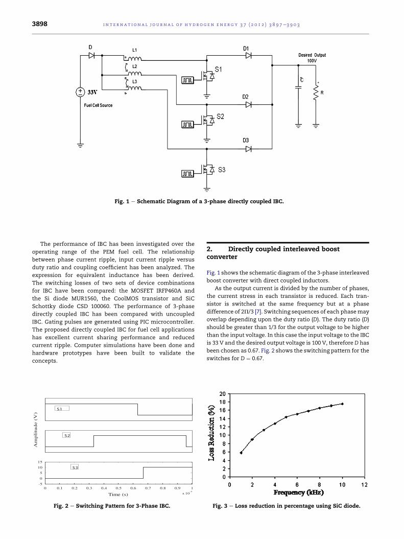
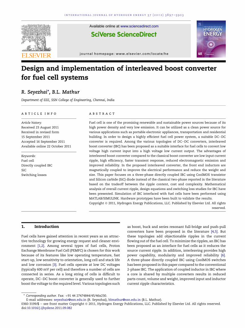
Fig. 1 e Schematic Diagram of a 3-phase directly coupled IBC.
i n t e rn a t i o n a l j o u r n a l o f h y d r o g e n en e r g y 3 7 ( 2 0 1 2 ) 3 8 9 7e3 9 0 33898
The performance of IBC has been investigated over the
operating range of the PEM fuel cell. The relationship
between phase current ripple, input current ripple versus
duty ratio and coupling coefficient has been analyzed. The
expression for equivalent inductance has been derived.
The switching losses of two sets of device combinations
for IBC have been compared: the MOSFET IRFP460A and
the Si diode MUR1560, the CoolMOS transistor and SiC
Schottky diode CSD 100060. The performance of 3-phase
directly coupled IBC has been compared with uncoupled
IBC. Gating pulses are generated using PIC microcontroller.
The proposed directly coupled IBC for fuel cell applications
has excellent current sharing performance and reduced
current ripple. Computer simulations have been done and
hardware prototypes have been built to validate the
concepts.
Fig. 2 e Switching Pattern for 3-Phase IBC.
2. Directly coupled interleaved boostconverter
Fig. 1 shows the schematic diagram of the 3-phase interleaved
boost converter with direct coupled inductors.
As the output current is divided by the number of phases,
the current stress in each transistor is reduced. Each tran-
sistor is switched at the same frequency but at a phase
difference of 2P/3 [7]. Switching sequences of each phasemay
overlap depending upon the duty ratio (D). The duty ratio (D)
should be greater than 1/3 for the output voltage to be higher
than the input voltage. In this case the input voltage to the IBC
is 33 V and the desired output voltage is 100 V, therefore D has
been chosen as 0.67. Fig. 2 shows the switching pattern for the
switches for D ¼ 0.67.
Fig. 3 e Loss reduction in percentage using SiC diode.
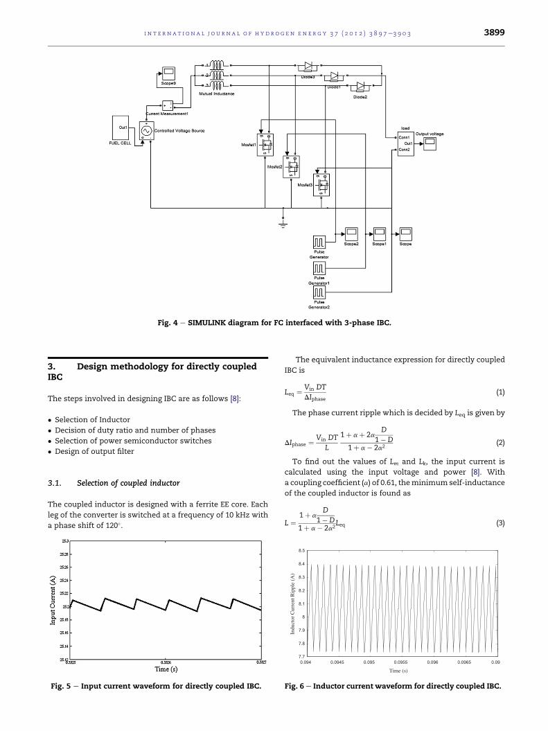
Fig. 4 e SIMULINK diagram for FC interfaced with 3-phase IBC.
i n t e r n a t i o n a l j o u r n a l o f h y d r o g e n en e r g y 3 7 ( 2 0 1 2 ) 3 8 9 7e3 9 0 3 3899
3. Design methodology for directly coupledIBC
The steps involved in designing IBC are as follows [8]:
� Selection of Inductor
� Decision of duty ratio and number of phases
� Selection of power semiconductor switches
� Design of output filter
3.1. Selection of coupled inductor
The coupled inductor is designed with a ferrite EE core. Each
leg of the converter is switched at a frequency of 10 kHz with
a phase shift of 120�.
Fig. 5 e Input current waveform for directly coupled IBC.
The equivalent inductance expression for directly coupled
IBC is
Leq ¼ Vin DTDIphase
(1)
The phase current ripple which is decided by Leq is given by
DIphase ¼ Vin DTL
1þ aþ 2aD
1� D1þ a� 2a2
(2)
To find out the values of Lm and Lk, the input current is
calculated using the input voltage and power [8]. With
a coupling coefficient (a) of 0.61, theminimumself-inductance
of the coupled inductor is found as
L ¼1þ a
D1� D
1þ a� 2a2Leq (3)
0.094 0.0945 0.095 0.0955 0.096 0.0965 0.097.7
7.8
7.9
8
8.1
8.2
8.3
8.4
8.5
Time (s)
Indu
ctor
Cur
rent
Rip
ple
(A)
Fig. 6 e Inductor current waveform for directly coupled IBC.
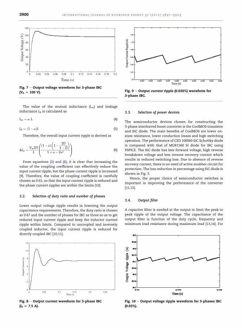
Fig. 9 e Output current ripple (0.026%) waveform for
3-phase IBC.
0 0.02 0.04 0.06 0.08 0.1 0.12 0.14 0.16 0.18 0.20
20
40
60
80
100
120
Time (s)
Out
put V
olta
ge (
V)
Fig. 7 e Output voltage waveform for 3-phase IBC
(V0 [ 100 V).
i n t e rn a t i o n a l j o u r n a l o f h y d r o g e n en e r g y 3 7 ( 2 0 1 2 ) 3 8 9 7e3 9 0 33900
The value of the mutual inductance (Lm) and leakage
inductance Lk is calculated as
Lm ¼ a$L (4)
Lk ¼ ð1� aÞL (5)
Therefore, the overall input current ripple is derived as
DIin ¼ VinDTL
0B@ð1� aÞ
�1� 2D
1� D
�
1þ a� 2a2
1CA (6)
From equations (2) and (6), it is clear that increasing the
value of the coupling coefficient can effectively reduce the
input current ripple, but the phase current ripple is increased
[9]. Therefore, the value of coupling coefficient is carefully
chosen as 0.61, so that the input current ripple is reduced and
the phase current ripples are within the limits [10].
3.2. Selection of duty ratio and number of phases
Lower output voltage ripple results in lowering the output
capacitance requirements. Therefore, the duty ratio is chosen
as 0.67 and the number of phases for IBC as three so as to get
reduced input current ripple and keep the inductor current
ripple within limits. Compared to uncoupled and inversely
coupled inductor, the input current ripple is reduced for
directly coupled IBC [10,11].
0 0.05 0.1 0.15 0.2 0.250
2
4
6
8
10
12
Time (s)
Out
put C
urre
nt (
A)
Fig. 8 e Output current waveform for 3-phase IBC
(I0 [ 7.5 A).
3.3. Selection of power devices
The semiconductor devices chosen for constructing the
3-phase interleaved boost converter is the CoolMOS transistor
and SiC diode. The main benefits of CoolMOS are lower on-
state resistance, lower conduction losses and high switching
operation. The performance of CSD 100060 SiC Schottky diode
is compared with that of MUR1560 Si diode for IBC using
PSPICE. The SiC diode has less forward voltage, high reverse
breakdown voltage and less reverse recovery current which
results in reduced switching loss. Due to absence of reverse
recovery current, there is no need of active snubber circuit for
protection. The loss reduction in percentage using SiC diode is
shown in Fig. 3.
Hence, the proper choice of semiconductor switches is
important in improving the performance of the converter
[11,12].
3.4. Output filter
A capacitor filter is needed at the output to limit the peak to
peak ripple of the output voltage. The capacitance of the
output filter is function of the duty cycle, frequency and
minimum load resistance during maximum load [13,14]. For
Fig. 10 e Output voltage ripple waveform for 3-phases IBC
(0.03%).
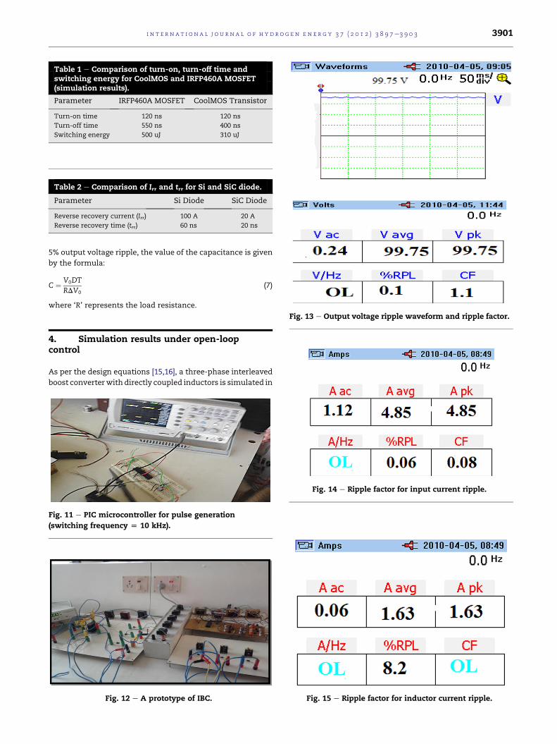
Table 1 e Comparison of turn-on, turn-off time andswitching energy for CoolMOS and IRFP460A MOSFET(simulation results).
Parameter IRFP460A MOSFET CoolMOS Transistor
Turn-on time 120 ns 120 ns
Turn-off time 550 ns 400 ns
Switching energy 500 uJ 310 uJ
Table 2 e Comparison of Irr and trr for Si and SiC diode.
Parameter Si Diode SiC Diode
Reverse recovery current (Irr) 100 A 20 A
Reverse recovery time (trr) 60 ns 20 ns
i n t e r n a t i o n a l j o u r n a l o f h y d r o g e n en e r g y 3 7 ( 2 0 1 2 ) 3 8 9 7e3 9 0 3 3901
5% output voltage ripple, the value of the capacitance is given
by the formula:
C ¼ V0DTRDV0
(7)
where ‘R’ represents the load resistance.
Fig. 13 e Output voltage ripple waveform and ripple factor.
4. Simulation results under open-loopcontrol
As per the design equations [15,16], a three-phase interleaved
boost converterwith directly coupled inductors is simulated in
Fig. 11 e PIC microcontroller for pulse generation
(switching frequency [ 10 kHz).
Fig. 12 e A prototype of IBC.
Fig. 14 e Ripple factor for input current ripple.
Fig. 15 e Ripple factor for inductor current ripple.
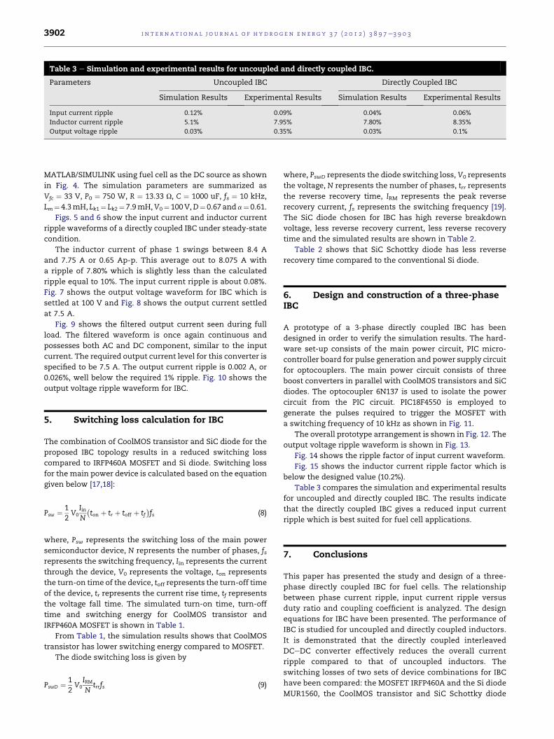
Table 3 e Simulation and experimental results for uncoupled and directly coupled IBC.
Parameters Uncoupled IBC Directly Coupled IBC
Simulation Results Experimental Results Simulation Results Experimental Results
Input current ripple 0.12% 0.09% 0.04% 0.06%
Inductor current ripple 5.1% 7.95% 7.80% 8.35%
Output voltage ripple 0.03% 0.35% 0.03% 0.1%
i n t e rn a t i o n a l j o u r n a l o f h y d r o g e n en e r g y 3 7 ( 2 0 1 2 ) 3 8 9 7e3 9 0 33902
MATLAB/SIMULINK using fuel cell as the DC source as shown
in Fig. 4. The simulation parameters are summarized as
Vfc ¼ 33 V, P0 ¼ 750 W, R ¼ 13.33 U, C ¼ 1000 uF, fs ¼ 10 kHz,
Lm¼ 4.3mH, Lk1¼ Lk2¼ 7.9mH,V0¼ 100V,D¼ 0.67 and a¼ 0.61.
Figs. 5 and 6 show the input current and inductor current
ripple waveforms of a directly coupled IBC under steady-state
condition.
The inductor current of phase 1 swings between 8.4 A
and 7.75 A or 0.65 Ap-p. This average out to 8.075 A with
a ripple of 7.80% which is slightly less than the calculated
ripple equal to 10%. The input current ripple is about 0.08%.
Fig. 7 shows the output voltage waveform for IBC which is
settled at 100 V and Fig. 8 shows the output current settled
at 7.5 A.
Fig. 9 shows the filtered output current seen during full
load. The filtered waveform is once again continuous and
possesses both AC and DC component, similar to the input
current. The required output current level for this converter is
specified to be 7.5 A. The output current ripple is 0.002 A, or
0.026%, well below the required 1% ripple. Fig. 10 shows the
output voltage ripple waveform for IBC.
5. Switching loss calculation for IBC
The combination of CoolMOS transistor and SiC diode for the
proposed IBC topology results in a reduced switching loss
compared to IRFP460A MOSFET and Si diode. Switching loss
for the main power device is calculated based on the equation
given below [17,18]:
Psw ¼ 12V0
IinN
�ton þ tr þ toff þ tf
�fs (8)
where, Psw represents the switching loss of the main power
semiconductor device, N represents the number of phases, fsrepresents the switching frequency, Iin represents the current
through the device, V0 represents the voltage, ton represents
the turn-on time of the device, toff represents the turn-off time
of the device, tr represents the current rise time, tf represents
the voltage fall time. The simulated turn-on time, turn-off
time and switching energy for CoolMOS transistor and
IRFP460A MOSFET is shown in Table 1.
From Table 1, the simulation results shows that CoolMOS
transistor has lower switching energy compared to MOSFET.
The diode switching loss is given by
PswD ¼ 12V0
IRMN
trrfs (9)
where, PswD represents the diode switching loss, V0 represents
the voltage, N represents the number of phases, trr represents
the reverse recovery time, IRM represents the peak reverse
recovery current, fs represents the switching frequency [19].
The SiC diode chosen for IBC has high reverse breakdown
voltage, less reverse recovery current, less reverse recovery
time and the simulated results are shown in Table 2.
Table 2 shows that SiC Schottky diode has less reverse
recovery time compared to the conventional Si diode.
6. Design and construction of a three-phaseIBC
A prototype of a 3-phase directly coupled IBC has been
designed in order to verify the simulation results. The hard-
ware set-up consists of the main power circuit, PIC micro-
controller board for pulse generation and power supply circuit
for optocouplers. The main power circuit consists of three
boost converters in parallel with CoolMOS transistors and SiC
diodes. The optocoupler 6N137 is used to isolate the power
circuit from the PIC circuit. PIC18F4550 is employed to
generate the pulses required to trigger the MOSFET with
a switching frequency of 10 kHz as shown in Fig. 11.
The overall prototype arrangement is shown in Fig. 12. The
output voltage ripple waveform is shown in Fig. 13.
Fig. 14 shows the ripple factor of input current waveform.
Fig. 15 shows the inductor current ripple factor which is
below the designed value (10.2%).
Table 3 compares the simulation and experimental results
for uncoupled and directly coupled IBC. The results indicate
that the directly coupled IBC gives a reduced input current
ripple which is best suited for fuel cell applications.
7. Conclusions
This paper has presented the study and design of a three-
phase directly coupled IBC for fuel cells. The relationship
between phase current ripple, input current ripple versus
duty ratio and coupling coefficient is analyzed. The design
equations for IBC have been presented. The performance of
IBC is studied for uncoupled and directly coupled inductors.
It is demonstrated that the directly coupled interleaved
DCeDC converter effectively reduces the overall current
ripple compared to that of uncoupled inductors. The
switching losses of two sets of device combinations for IBC
have been compared: the MOSFET IRFP460A and the Si diode
MUR1560, the CoolMOS transistor and SiC Schottky diode

i n t e r n a t i o n a l j o u r n a l o f h y d r o g e n en e r g y 3 7 ( 2 0 1 2 ) 3 8 9 7e3 9 0 3 3903
CSD 100060. The choice of SiC diode and CoolMOS transistor
for IBC has led to reduced switching losses. From these
results, directly coupled IBC with CoolMOS transistor and
SiC diode proves to be a suitable candidate for fuel cell
interface.
r e f e r e n c e s
[1] Jain IP. Hydrogen the fuel for 21st century. Int J HydrogenEnergy 1990;15(5):345e8.
[2] Winter CJ. Hydrogen energy-abundant, efficient, clean:a debate over the energy system of change. Int J HydrogenEnergy July 2009;34(14):S1e52.
[3] Peighambardoust SJ, Rowshanzamir S, Amjadi M. Reviewof the proton exchange membranes for fuel cellapplications. Int J Hydrogen Energy Sept.2010;35(17):9349e84.
[4] Kovacevic G, Tenconi A, Bojoi R. Advanced DC-DC converterfor power conditioning hydrogen fuel cell systems. Int JHydrogen Energy June 2008;33(12):3215e9.
[5] Choe GY, Kang HS, Lee BK, Lee WL. Design consideration ofinterleaved converters for fuel cell applications. IEEE ICEMS;2007:238e43. Seoul.
[6] Kosai H, McNeal S, Page A, Jordan B, Scofield J, Ray. B.Characterizing the effects of inductor coupling on theperformance of an interleaved boost converter. CARTS USA;2009:237e51.
[7] Shin HB, Park JG, Chung SK, Lee HW, Lipo TA. Generalizedsteady-state analysis of multiphase interleaved boostconverter with coupled inductors. IEE Electronics Power Appl2005;152(3):584e94.
[8] Lee P, Lee Y, Cheng DKW, Liu X. Steady-state analysis of aninterleaved boost converter with coupled inductors. IEEETrans Ind Electron 2000;47(4):787e95.
[9] Huber L, Irving BT, Jovanovic. MM. Closed-loop controlmethods for interleaved DCM/CCM boundary boost PFCconverters. IEEE APEC; 2009:991e7.
[10] Thounthong P, Sethakul P, Rael S, Davat B. Design andimplementation of 2-phase interleaved boost converter forfuel cell power source. IET ICPEMD; 2008:91e5.
[11] Xu H, Qiao E, Guo X, Wen X, Kong L. Analysis and design ofhigh power interleaved boost converters for fuel celldistributed generation system. IEEE PESC; 2005:140e5.
[12] Veerachary M, Senjyu T, Uezato K. Modeling and analysis ofinterleaved dual boost converter. IEEE ISIE June 2001;2:718e22. 2001.
[13] Veerachary M, Senjyu T, Uezato K. Small-signal analysis ofinterleaved dual boost converter. Int J Circuit TheoryApplications 2001;29(6):575e89.
[14] Wai RJ, Duan RY. High step-up converter with coupled-inductor. IEEE Trans Power Electronics 2005;20(5):1025e35.
[15] Dahono PA, Riyadi S, Mudawari A, Haroen. Y. Outputs rippleanalysis of multiphase DC-DC converter. IEEE ICPEDS; 1999:626e31.
[16] Miwa BA, Dtten DM, Schlecht. MF. High efficiency powerfactor correction using interleaving technique. IEEE APEC1999;1:557e68.
[17] Todorovic MH, Palma L, Enjeti PN. Design of a wide inputrange DC-DC converter with a robust power control schemesuitable for fuel cell power conversion. IEEE Trans IndElectron 2008;55(3):1247e55.
[18] Luo FL, Hong Ye, Rashid. M. Digital power electronics andapplications. Academic Press; 2009.
[19] Erickson RW, Maksimovic D. Fundamentals of powerelectronics. 2nd ed. Kluwer Academic Publishers; 2001.