
Design and Functionality of Capacitive Micromachined ...
19
Design and Functionality of Capacitive Micromachined Ultrasonic Transducers for Underwater Applications Mason Valdisera and William Leisner MEMS 1082 December 6 th , 2018
Transcript of Design and Functionality of Capacitive Micromachined ...

Design and Functionality of Capacitive
Micromachined Ultrasonic Transducers for
Underwater Applications
Mason Valdisera and William Leisner
MEMS 1082
December 6th, 2018

Abstract
The capacitive micromachined ultrasonic transducer (CMUT) can be used in
underwater applications, mainly imaging. The CMUT is an alternative technology to
piezoelectric transducers, offering advantages such as wider bandwidths, ease of
fabricating large arrays, and the potential for integration with electronic circuits. The
transducer works by emitting an ultrasonic wave to penetrate murky water: increasing
image visibility, clarity, and range. There are a wide array of applications for this device
such as underwater observation, differentiating objects, and recreational activities. The
CMUT uses a combination of silicon, silicon dioxide, electrodes, and a gap (either
vacuum or air) to create the capacitive circuit.
CMUTs have been used in the biomedical field before, but new technologies that
seal the chamber allow this device to now be used underwater. The report will highlight
the principles behind the CMUT in underwater applications and the different
components involved that allow it to function properly. Also, the various ways to
fabricate a CMUT including sacrificial layer deposition and the wafer bonding method
will be detailed. Within each design and method there are advantages and drawbacks
that will be considered and expanded upon.

Introduction
CMUTs are an emerging transducer, and have recently been adapted for
underwater use, allowing scientists to explore their possibilities in a new field of
application, underwater imaging. Currently, piezoelectric micromachined ultrasonic
transducers (PMUTs) are the dominant ultrasonic transducer technology used in
underwater imaging and other applications [1]. They are based on lead zirconate
titanate (PZT). However, PZT based acoustic transducers have several drawbacks
such as low operational efficiency, narrow operating bandwidths, and difficulty in
processing two-dimensional arrays [1]. On the other hand, CMUTs have several
advantages over PMUTs. They have better matching with the acoustic impedance of
air and other fluids without needing a surface matching layer. They also have a large
immersion bandwidth and high electromechanical coefficient, which means an improved
image quality. Further, CMUTs have high directivity, a wide operating temperature
range, compatibility with integrated circuits, and low-cost manufacturing possibilities [2].
However, for CMUTs to truly replace PMUTs, CMUT transducer arrays need
improved bandwidth, sensitivity, directivity, and output pressure. These are all linked to
improved image quality. Improved ultrasonic transducers have the potential to benefit
fields such as sonar and high resolution imaging, non-destructive testing, and high
frequency medical imaging [3].
This paper will go over the history of CMUTs since their inception, highlighting
the changes and improvements in their design and manufacture. Then it will detail the
theory of CMUTs, giving an in-depth explanation of how they work. Then manufacturing

will be revisited with a look at how specific manufacturing methods work. Next, a
detailed look at the applications of CMUTs will be discussed.
History
Ultrasonic devices have been used for underwater imaging since the end of
World War I following the advent of the modern submarine. Ultrasonic devices have
also been used in medicine since the 1930s, most notably the use of ultrasound
imaging (sonography) to view a developing fetus was invented in the 1950s. Today,
ultrasonic devices continue to play a large role on submarines and surface craft sonar
systems.
The first capacitive ultrasonic transducer was developed in 1989 by Hohm and
Hess. In 1994, Haller and Khuri-Yakub developed the first CMUT using sacrificial layer
technology and with a sealed cavity, meaning it could be used for underwater
applications. In 2003, a wafer bonding technology to reduce process steps and improve
the quality of the product was developed. In 2006, Chang et al. developed a polymer
based CMUT using a sacrificial layer technique and fabricated on a polymer substrate,
allowing the CMUT to be flexible. CMUTs on very thin silicon also have bending
characteristics. In 2008, flexible CMUT arrays were fabricated by etching trenches into
a silicon wafer and filling them with polydimethylsiloxane (PDMS). Also in 2008, a
lamination technique was used to minimize residual stress to fabricate bonding
structures at low temperatures and pressures. In 2012, PDMS and bonding technology
were used to create a stretchable CMUT. In 2017, a low temperature roll-lamination
technique and silver nanowire electrodes were used to produce a transparent and
flexible CMUT [4].

Theory
A CMUT is a capacitor cell that consists of a thin moveable plate suspended over
a vacuum gap. A metal coating on the thin plate or the thin plate itself acts as the top
electrode for the capacitor. An underlying conductive substrate acts as the bottom
electrode. By applying a DC voltage, the two electrodes are attracted to one another,
but they are restricted by a restoring force caused by the stiffness of the plate. If AC
voltage is used to drive the capacitor it generates ultrasound. If the capacitor is
subjected to an ultrasonic pressure, a current is induced due to the capacitive change of
the device.
The goal of an electrostatic transducer is to operate at a high electrical field. The
ability of the CMUT to produce this high electrical field (> 108 V/cm) makes it a
competitive device compared to other electrostatic transducers. By operating with a
high electrical field, the device must be handled with extreme care in order to maintain
its accuracy and function. The frequency of the CMUT is determined mainly by the size,
shape, and material properties of the thin plate. Often times an array of thin plates with
different shapes and sizes are put in parallel to allow the device to operate at various
frequencies.
The transducer can be covered with a thin layer of elastic polymer to provide
electrical insulation for the device. The CMUT has a very large bandwidth which gives it
a distinct advantage over piezoelectric devices which have smaller bandwidths. The
broad bandwidth is due to the fact that the mechanical impedance of the plate is
significantly lower than the loading impedance. The lower cutoff frequency is
determined by the spring constant of the device. As the spring constant increases, the
bandwidth of the CMUT decreases. Selecting the correct rod, with a specific spring
constant, that will support the device, but also maintain the broad bandwidth must be
analyzed when constructing the CMUT. The higher cutoff frequency is determined by
the mass loading of the immersion medium [5].
When used in underwater imaging, CMUTs are paired, with one group
transmitting and the other group receiving. A transducer operating in transmitting mode
requires a high cavity height to obtain high output pressure, while a transducer working
in receiving mode requires only a low cavity height to attain high sensitivity [1]. When
the size of the top electrode is 40% to 50% of the size of the membrane, the transducer
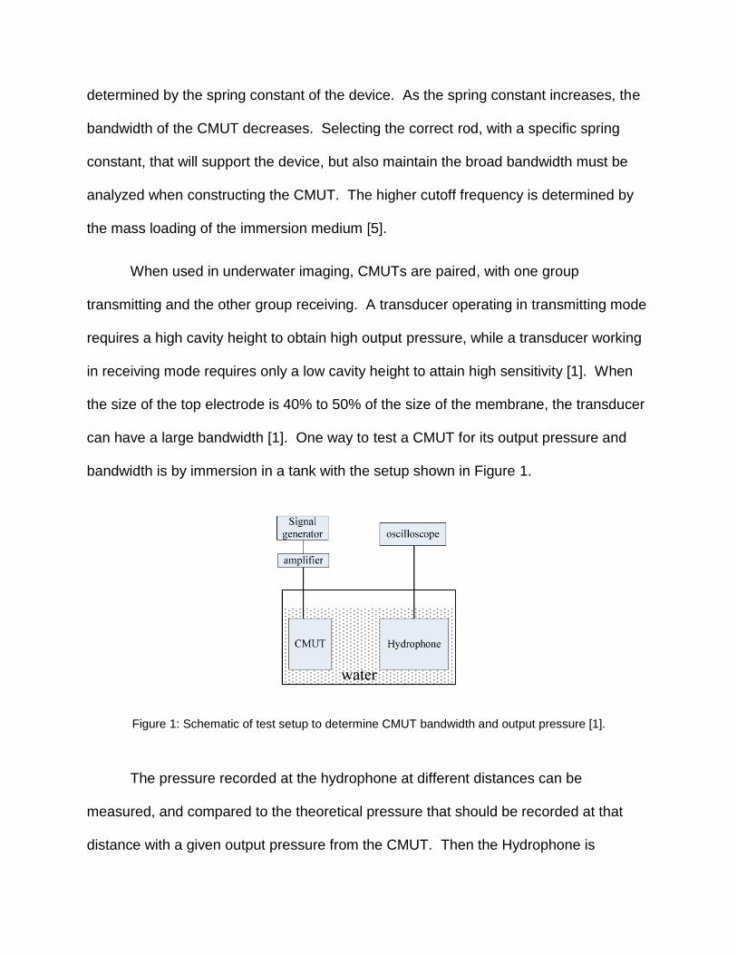
can have a large bandwidth [1]. One way to test a CMUT for its output pressure and
bandwidth is by immersion in a tank with the setup shown in Figure 1.
Figure 1: Schematic of test setup to determine CMUT bandwidth and output pressure [1].
The pressure recorded at the hydrophone at different distances can be
measured, and compared to the theoretical pressure that should be recorded at that
distance with a given output pressure from the CMUT. Then the Hydrophone is

replaced by another CMUT, and the distance can be measured by taking the time it
takes for the receiver CMUT to pick up the transmitted signal sent by the transmitting
CMUT. This time can be multiplied by the speed of sound in the water, giving the
distance.
Figure 2: Transmission and Reception of CMUT [6]
The major difference between the CMUT that transmits and the CMUT that
receives is that the receiver is a sensor and the transmitter is an actuator. In the
receiver, the ultrasonic wave causes the beam to vibrate which induces a capacitance
change. The beam vibration causes the capacitance change because the gap between
the two plates fluctuate as the beam vibrates. Equation 1 shows the relationship
between the capacitance, C, and the gap thickness, t.
𝐶 =𝜖𝐴
𝑡 (1)
The beam vibration causes t to change which would then change the
capacitance value. The change in capacitance is then used to create a change in
voltage across the device. Equation 2 shows the relationship between voltage and
capacitance.

𝑄 = 𝐶𝑉 (2)
The charge remains constant across the capacitor, so changing the capacitance
changes the voltage. In the transmitter, the voltage is not used as an output, rather the
driving input signal. The AC voltage applied to the beam causes the capacitance to
change using equation 2. With a change in capacitance, using equation 1, the gap
thickness must change. The constantly changing gap thickness causes the beam to
vibrate. If the input voltage is at a high enough frequency, the beam will vibrate at a
frequency high enough to induce an ultrasonic wave.
When the transmitter emits an ultrasonic wave, if the wave comes in contact with
an object it will bounce back toward the CMUT. The bounced back wave will then be in
contact with the receiver. The time from when the transmitter emits the ultrasonic wave
to when the voltage across the receiver changes is recorded to calculate the distance
away that an object is.
For a CMUT transducer used in underwater imaging, important parameters to
determine are the axial (∆x) and lateral (∆y) resolutions. These are the minimum
distances that can be distinguished between two echo sources. The ∆x and ∆y
resolutions are determined using Equations 3 and 4 respectively. For Equation 3, n is
the number of scanning lines, λ is the wavelength and nλ is the pulse width. For
Equation 4, D is the aperture size of the probe and S is the distance between the focus
and the CMUT [1].
𝛥𝑥 =
𝑛𝜆
2
(3)

𝛥𝑦 =
1.22𝜆
𝐷 𝑆
(4)
Increasing the operating frequency (reducing wavelength) and reducing scanning lines
decreases (improves) the axial resolution. At a specific focus, increasing aperture size
and reducing wavelength improve the lateral resolution.
Manufacturing
The first CMUTs were fabricated using conventional machining tools. A rough
metal surface was the back plate of the capacitor and the top electrode consisted of a
metallized Mylar membrane [7]. Micromachining replaced conventional machining to
create cavities in silicon, but metallized dielectric films were still used as the membrane
material, preventing vacuum sealing. In 1994, the first fully micromachined CMUT was
created using the sacrificial release method.
Sacrificial release methods vary, but all follow essentially the same principles.
Sacrificial release is a type of surface micromachining. In surface micromachining,
microstructures are built via deposition and etching of structural layers over a substrate,
or the base material of the structure, which is usually made of silicon. In the fabrication
process, sacrificial layers (typically oxides) are layers that are applied to allow the
deposition of structural layers (typically poly-silicon), but are then removed to leave
behind just the structural material, creating desired cavities and voids. Surface
micromaching is illustrated in Figure 3.

Figure 3: Illustration of surface micromachining [8].
This is not the same as bulk micromachining, where a substrate is selectively
etched either chemically or physically to create miniaturized mechanical components.
There are low and high temperature sacrificial release methods, with lower
temperatures allowing the CMUT to be manufactured on the same silicon wafer as other
electronics, allowing for integration with electronics. For the process to be done on
electronic bearing wafers, the highest temperature at any point in the process cannot
exceed 400°C [7]. A high temperature process developed at Stanford University is an
example of a popular sacrificial release method.
The process begins with a silicon wafer that has been doped so as to be highly
conductive on its surface. This forms the back electrode of the CMUT. Next, the wafer
is then deposited with an etch-stop layer of silicon nitride (Si3N4) at 785°C with low
pressure chemical vapor deposition (LPCVD). Then the sacrificial-layer depositioning
and patterning is done in two steps so that the channels used by potassium hydroxide
(KOH) to remove the sacrificial layer are thinner than the cavity thickness. First, a layer
of LPCVD poly-silicon is deposited and photolithography is used to define regions of
reduced channel height. Then a dry etch removes all of the poly-silicon in the defined
regions, stopping at the Si3N4 layer. Next, another layer of poly-silicon is deposited.
The thickness of this layer determines the thickness of the etch channels while the

thickness of both layers combined determines the initial cavity height. These
depositions are often done at lower temperatures because this allows for better
thickness control [7]. Then, another photolithography and dry etch are done to define
the cavity and membrane shape. The membrane shape is a hexagon or circle because
it is easy to model. It is important to note that the shape and size of the membrane are
important design parameters that determine the frequency response of the CMUT
element [7]. Next, a critical membrane layer is deposited. It is an etch-stop layer of
Si3N4 that is deposited by LPCVD at 785°C, similar to the first one deposited on the
wafer. After this, another lithography and dry etch step creates small holes in the etch-
stop layer. These holes are located over the etch channels, and are to allow the KOH
to pass bellow the critical membrane to etch out the cavity beneath. Then the wafer is
immersed in KOH for anywhere from a few hours to a few days depending on the
temperature, which drives the poly-silicon etch rate of KOH.
Once the etching is complete, the holes are sealed by a layer of Si3N4 in another
step of LPCVD. Not only does this seal the holes, but since the process occurs at
extremely low pressures, the cavities are considered to be vacuum sealed [7]. This is
the essential step in creating a CMUT that can be used in immersion applications since
the sealed cavity will maintain its vacuum, not filling with whatever fluid the CMUT is
immersed in. The rest of the process creates electrical connections from the bond pads
to the top and bottom electrodes. First, a lithography and etch step creates connections
to the ground plane through the Si3N4 layers. Then aluminum is sputtered over the
wafer and patterned using lithography and a wet etch. The final step is an optional
annealing step that improves the ohmic contact to ground of the CMUT but also
introduces high levels of stress to the component. This step is done or left out
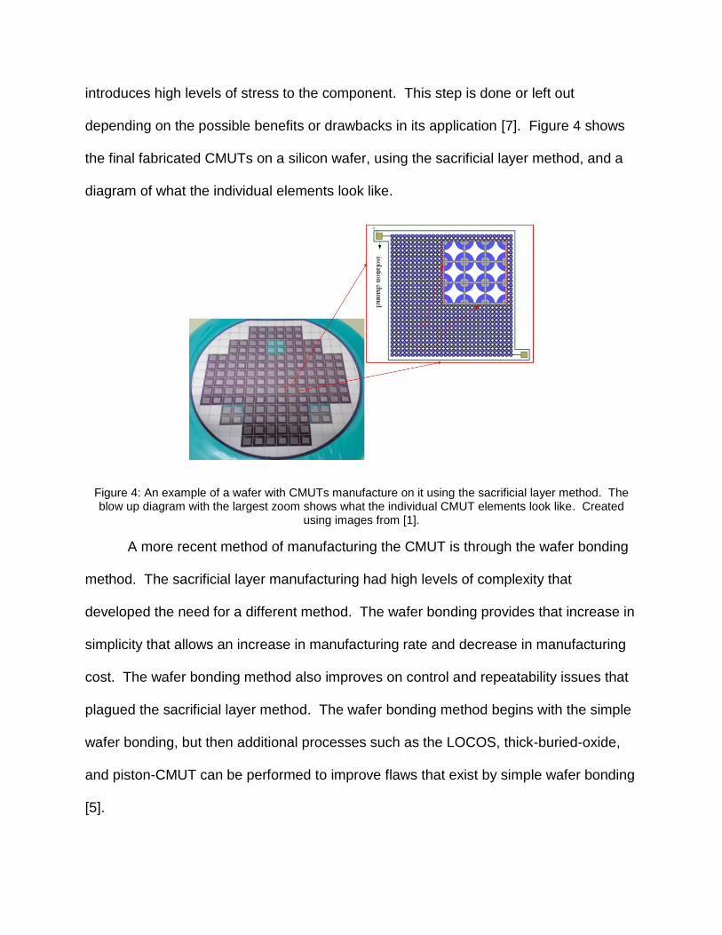
depending on the possible benefits or drawbacks in its application [7]. Figure 4 shows
the final fabricated CMUTs on a silicon wafer, using the sacrificial layer method, and a
diagram of what the individual elements look like.
Figure 4: An example of a wafer with CMUTs manufacture on it using the sacrificial layer method. The blow up diagram with the largest zoom shows what the individual CMUT elements look like. Created
using images from [1].
A more recent method of manufacturing the CMUT is through the wafer bonding
method. The sacrificial layer manufacturing had high levels of complexity that
developed the need for a different method. The wafer bonding provides that increase in
simplicity that allows an increase in manufacturing rate and decrease in manufacturing
cost. The wafer bonding method also improves on control and repeatability issues that
plagued the sacrificial layer method. The wafer bonding method begins with the simple
wafer bonding, but then additional processes such as the LOCOS, thick-buried-oxide,
and piston-CMUT can be performed to improve flaws that exist by simple wafer bonding
[5].

The simple wafer bonding method begins with two wafers, a high quality silicon
wafer and a silicon-on-insulator wafer. The cavity is created on the high quality silicon
wafer by etching thermal oxide down onto the substrate. The insulation layer is grown
by inducing a second thermal oxidation [5]. The two silicon wafers are then placed
together in vacuum. The wafers are subjected to high temperatures (around 1000°C) to
form strong covalent bonds. The handle and the etched thermal oxide layer are
removed from the silicon-on-insulator wafer leaving a thin, single layer silicon crystal
suspended over the cavity. The electrical connections between the substrates are
created through opening in the oxide layer. Deep trenches are etched into the silicon
wafer to define silicon pillars that serve to establish interconnection between different
elements within the CMUT. Because the suspended layer is a single crystal, the
thickness, uniformity, and mechanical properties of the plate are well controlled. Also,
the gap height of the CMUT is well controlled [5]. These provide distinct advantages
over the sacrificial layer technique. There are also drawbacks to this method. The
minimum gap height remains limited by the thickness of the initial oxide layer. The
interconnection struggle is vulnerable to shorts that can occur when the device
becomes contaminated. The contamination can occur when handling the device,
storing the device, or packaging the device [5].
The LOCOS process includes an extended insulation layer in the post area to
address the low breakdown voltage issue associated with the simple wafer bonding
method. The extended layer is formed through local oxidation of silicon (LOCOS). This
process maintains the precise gap control from the simple wafer bonding [5].

The thick-buried-oxide process seeks to further reduce the dielectric breakdown
by isolating the bottom electrode to the region where the electric field needs to be high.
This removes a high electric field in unnecessary areas. This method works by applying
a thick buried oxide layer on the silicon-on-insulator wafer. The arrangement allows for
each cell to have its own connection with the electrode [5].
The final improvements can be made to the CMUT by improving the structure of
the device. One such improvement involves forming the central mass by etching the
device layer of an SOI layer or by plating metal on top of the plate structure [5]. The
added mass shows improved performance and a wider bandwidth. Another
improvement involves adding long, narrow posts to provide the spring constant for the
device. Both additions cause a more flexible design space and separate the mass and
spring components [5].
Figure 5: Diagrams of all the Manufacturing Techniques. (a) Sacrificial Layer Method, (b) Simple Wafer Bonding, (c) LOCOS Process, (d) Thick-Buried-Oxide Process, (e) Adding Mass to Plate, (f) Lengthening
and Narrowing of the Posts.
In 2017, Pang et al. developed a transparent, flexible CMUT using a roll-
lamination technique [4]. In roll-lamination, there are two important steps. The first, is

to prepare vibrating membranes on a PET release layer. The second step is to
laminate these membranes onto a sidewall. The temperatures and pressures are
careful controlled to ensure that the vibrating membrane bonds to the sidewall. The
vibrating membrane is the CMUT and the sidewall provides structural support. Silver
nanowires were used as the electrodes since they are transparent to the human eye.
The completed transparent, flexible CMUT is shown in Figure 6.
Figure 6: A transparent, flexible CMUT fabricated using a roll-lamination method [4].
Applications
The CMUT covers a wide range of applications, and improved designs have
created new possibilities in the applications that it serves. Many applications include
imaging, as the CMUT is able to resolve clear images in small or low-visibility locations.
The CMUT was initially designed for air coupled applications. However, it began to shift
towards medical and underwater applications.
The CMUT device works well for the medical industry because it is able to take
images of moving internal structures. The CMUT equipment is cost-effective and
portable, which makes the device even more appealing to the medical industry. For
these reasons, CMUT imaging is used in cardiac structures, the vascular system, the

fetus and uterus, abdominal organs such as the liver, the kidneys and gall bladder, and
the eye [5].
In 1994, Khuri-Yakub led his team to create the first CMUT with a sealed cavity
[1]. The CMUT will scan across a specified distance underwater and any objects that
are within this range will be displayed. The imaging device utilizes the two CMUT
devices, one transmitter and one receiver, as stated in the theory section [1]. The two
transducers move laterally to scan a certain range of distances. Figure 7 shows the
result of using a CMUT underwater to detect a target object. From the image, the target
is clearly displayed by the white markings. The axial and lateral distance plots give the
spatial location of the target relative to the CMUT. Although the edges of the image
remain blurred, the CMUT undoubtedly identifies the target while submerged in water
[1]. When the water is too murky for regular cameras and imaging to work, the CMUT
can provide this plot to accurately display what objects are nearby and where they are
located. The distances measured compared to the CMUT when tested showed roughly
1 cm in error [1].
Figure 7: Plot showing detection and position of object underwater [1].

There are broad uses for underwater imaging including the commercial,
scientific, and military industries [3]. The commercial industry would use the imaging to
identify where fish or any other catch are located. The CMUT imaging will improve the
efficiency of fishing, especially in areas with murky water. The scientific application of
the CMUT imaging includes studying underwater habitats and ship wreck locations.
Coral reef destruction has been a topic of concern, and with the CMUT imaging, the
size and status of a coral reef can be monitored. Additionally, the CMUT can be used to
study a shipwreck. Often the locations of sunken ships are dark, with extremely low
visibility. Using the CMUT imaging, the location of wrecked ships can be found [3].
Finding the ships allows for them to be studied and explain why the ship was wrecked.
The other application of the CMUT imaging would be for military purposes [3]. The
imaging can be used to detect enemy submarines. Knowing the location of an enemy
vessel gives the CMUT user a tactical advantage.
Figure 8: Different applications of underwater imaging [3].

Conclusion
In conclusion, the CMUT utilizes a capacitor cell with a thin movable plate to emit
ultrasonic waves for various imaging applications. The CMUT has distinct advantages
over piezoelectric counterparts such as cost, manufacturability, and range of
applications. The CMUT has become increasingly popular in underwater imaging with
the breakthrough of sealing the chamber of the capacitive device. Objects that lie in
murky water can be clearly identified using the CMUT. There are various reasons to
need the clear underwater imaging such as studying marine biology, naval use, and
even for recreational activity. With continual developments in manufacturing, the CMUT
has increased its broad frequency bandwidth, sensitivity, and flexibility. While the
CMUT succeeds in identifying underwater objects, it must continue to undergo testing
and analysis to further improve the clarity of the images themselves. This can be done
my modifying the 2-D arrays in the CMUT. Already a leader in underwater applications,
further improvements will make the CMUT the best option for underwater imaging.
References
[1] Song, Jinlong et al. “Capacitive Micromachined Ultrasonic Transducers (CMUTs) for
Underwater Imaging Applications.” www.mdpi.com/journal/sensors.
[2] Zhang, Rui et al. “Design and performance analysis of capacitive micromachined
ultrasonic transducer (CMUT) array for underwater imaging.” Microsyst Technol, 16
November, 2015.
[3] Oralkan, Ömer et al. “Underwater Acoustic Imaging using Capacitive Micromachined
Ultrasonic Transducer Arrays.” https://web.stanford.edu/group/khuri-
yakub/publications/02_Oralkan_02.pdf
[4] Pang, Da-Chen. Chang, Cheng-Min. “Development of a Novel Transparent Flexible
Capacitive Micromachined Ultrasonic Transducer.” Department of Mechanical
Engineering, National Kaohsiung University of Applied Sciences, 20 June, 2017.
[5] Khuri-Yakub, Butrus and Oralkan, Ömer. “Capacitive Micromachined Ultrasonic
Transducers for Medical Imaging and Therapy.” https://www.ncbi.nlm.nih.gov/pmc/articles/PMC3158704/
[6] Bekkers, Paul. “CMUT Ultrasound Breakthrough Technology.”
https://www.innovationservices.philips.com/looking-expertise/mems-micro-
devices/mems-applications/capacitive-micromachined-ultrasonic-transducers-cmut/
[7] Ergun et al. “Capacitive Micromachined Ultrasoni Transducers: Fabrication Technology.
[8] “Fabricating MEME and Nanotechnology.” MEMS & Nanotechnology Exchange,
Accessed 3 December, 2018. Available: https://www.mems-
exchange.org/MEMS/fabrication.html


![[105]-Design and Performance Analysis of Capacitive Micromachined Ultrasonic Transducer Linear Array](https://static.fdocuments.net/doc/165x107/56d6bddc1a28ab30168f9c62/105-design-and-performance-analysis-of-capacitive-micromachined-ultrasonic.jpg)


