Design and Fabrication of a Strain-Powered ... and Fabrication of a Strain-Powered...
34
Design and Fabrication of a Strain-Powered Microelectromechanical System (MEMS) Switch by Cory R Knick and Christopher J Morris ARL-TR-7095 September 2014 Approved for public release; distribution unlimited.
Transcript of Design and Fabrication of a Strain-Powered ... and Fabrication of a Strain-Powered...

Design and Fabrication of a Strain-Powered
Microelectromechanical System (MEMS) Switch
by Cory R Knick and Christopher J Morris
ARL-TR-7095 September 2014 Approved for public release; distribution unlimited.

NOTICES
Disclaimers The findings in this report are not to be construed as an official Department of the Army position unless so designated by other authorized documents. Citation of manufacturer’s or trade names does not constitute an official endorsement or approval of the use thereof. Destroy this report when it is no longer needed. Do not return it to the originator.
Army Research Laboratory Adelphi, MD 20783-1138
ARL-TR-7095 September 2014
Design and Fabrication of a Strain-Powered Microelectromechanical System (MEMS) Switch
Cory R Knick and Christopher J Morris
Sensors and Electron Devices Directorate, ARL Approved for public release; distribution unlimited.

ii
REPORT DOCUMENTATION PAGE Form Approved OMB No. 0704-0188
Public reporting burden for this collection of information is estimated to average 1 hour per response, including the time for reviewing instructions, searching existing data sources, gathering and maintaining the data needed, and completing and reviewing the collection information. Send comments regarding this burden estimate or any other aspect of this collection of information, including suggestions for reducing the burden, to Department of Defense, Washington Headquarters Services, Directorate for Information Operations and Reports (0704-0188), 1215 Jefferson Davis Highway, Suite 1204, Arlington, VA 22202-4302. Respondents should be aware that notwithstanding any other provision of law, no person shall be subject to any penalty for failing to comply with a collection of information if it does not display a currently valid OMB control number. PLEASE DO NOT RETURN YOUR FORM TO THE ABOVE ADDRESS.
1. REPORT DATE (DD-MM-YYYY)
September 2014 2. REPORT TYPE
Final 3. DATES COVERED (From - To)
11/2013 to 08/2014 4. TITLE AND SUBTITLE
Design and Fabrication of a Strain-Powered Microelectromechanical System (MEMS) Switch
5a. CONTRACT NUMBER
5b. GRANT NUMBER
5c. PROGRAM ELEMENT NUMBER
6. AUTHOR(S)
Cory R Knick and Christopher J Morris 5d. PROJECT NUMBER
5e. TASK NUMBER
5f. WORK UNIT NUMBER
7. PERFORMING ORGANIZATION NAME(S) AND ADDRESS(ES)
U.S. Army Research Laboratory ATTN: RDRL-SES-L 2800 Powder Mill Road Adelphi, MD 20783-1138
8. PERFORMING ORGANIZATION REPORT NUMBER ARL-TR-7095
9. SPONSORING/MONITORING AGENCY NAME(S) AND ADDRESS(ES)
10. SPONSOR/MONITOR'S ACRONYM(S)
11. SPONSOR/MONITOR'S REPORT NUMBER(S)
12. DISTRIBUTION/AVAILABILITY STATEMENT
Approved for public release; distribution unlimited. 13. SUPPLEMENTARY NOTES
14. ABSTRACT
Microelectromechanical systems (MEMS) switches, while having the potential to function under ultra low power constraints, still require onboard power sources. Strain-powered actuators can be triggered with off-board power sources such as laser irradiation. In this report, we discuss the design and fabrication of a microswitch that could eventually be optically triggered to fold using the heat generated from a laser. These switches were fabricated on a silicon wafer using standard microfabrication techniques. We discuss in detail switch design and fabrication process as well as the evolution of design changes implemented to overcome process and design issues. We have taken an initially rather complex, process-intensive design and reduced it to a process requiring only lift-off for patterning. We show that an actuated switch would have a resistance of 40 ohms with 10 mA applied across the contacts. 15. SUBJECT TERMS
MEMS, optical actuation, microelectromechanical system, micro-switch, microfabrication
16. SECURITY CLASSIFICATION OF: 17. LIMITATION
OF ABSTRACT
UU
18. NUMBER OF
PAGES
34
19a. NAME OF RESPONSIBLE PERSON
Cory R Knick a. REPORT
Unclassified b. ABSTRACT
Unclassified c. THIS PAGE
Unclassified 19b. TELEPHONE NUMBER (Include area code)
301-394-1147 Standard Form 298 (Rev. 8/98) Prescribed by ANSI Std. Z39.18

iii
Contents
List of Figures iv
1. Introduction 1
1.1 Design ..............................................................................................................................1
1.2 Fabrication .......................................................................................................................2
1.3 Electrical Characterization Methods ...............................................................................4
2. Results and Discussion 4
2.1 Electrical Characterization ..............................................................................................4
2.2 Fabrication Challenges ....................................................................................................6
3. Conclusions 13
4. References 14
Appendix A. Process Sheet for Lift-Off Only Process (Wafers # 25, 26) 17
Appendix B. Process Sheet for Ion Mill and Electroplating Process 21
List of Symbols, Abbreviations, and Acronyms 24
Distribution List 25

iv
List of Figures
Fig. 1 Calculated fold angles for a fold-up stack of 10/120/50/10 nm Cr/Au/Cr/Au (blue) and a fold-down stack of 10/120 nm Cr/Au (red). This stack is advantageous for at least two considerations; 1) a common base layer of Cr/Au is shared among fold-up and fold-down hinges and 2) significant folding is predicted for relatively short hinges (i.e., 45° at 25 µm). .......................................................................................................................................2
Fig. 2 Process flow for MEMS switch version 1 with electroplated Au frames; a) lift-off contacts, b) lift-off sacrificial Si, c) blanket evaporate Cr/Au fold-down layer, d) lift-off Cr/Au fold-up layer, e) electroplate Au frames, f) wet etch or ion mill, g) develop 1827 resist hinge, and h) XeF2 dry etch Si to release the switch ........................................................3
Fig. 3 Process flow for MEMS switch version 2 without electroplated Au frames; a) lift-off contacts, b) lift-off sacrificial Si, c) lift-off Cr/Au fold-down layer, d) lift-off Cr fold-up layer, e) develop resist, and f) dry etch release ..........................................................................3
Fig. 4 Switch resistance vs. number of cycles of the XeF2 etch from devices corresponding to a fabrication run carried out using the ion mill patterning steps and electroplating ..............5
Fig. 5 SEM of a dry etched switch device corresponding to resistance measurements presented in Fig. 4. .....................................................................................................................6
Fig. 6 Switch after Cr/Au wet-etch process step. Wet etching undercut the switch features, removing significant amounts of the thin films required to actuate the switch. Wet etching also showed poor selectivity, resulting in etching of the Au electrical contacts that were lifted off in the previous step. ....................................................................................................7
Fig. 7 SEM images of a wet-etched device after XeF2 dry etch, (left) Au frame is attacked from wet etch at sidewalls and the Au contact is mostly etched away; (right) side view, unclear whether Si is completely undercut from the dry etch ...................................................7
Fig. 8 SEM of switch patterned by ion milling, showing cleaner sidewalls and a well-defined switch geometry. Au contact lines are still intact, further demonstrating that ion milling is superior to wet etching. Right: switch folding after dry etch release. .......................8
Fig. 9 Array of test cantilevers on Au contacts after dry etch release showing uniform folding upwards; the top edge appears to be anchored to the substrate, which necessitated a mask rewrite after reducing dimensions of the second PVD step ...........................................8
Fig. 10 Problems encountered during the lift-off process run; underdeveloped resist causing the switch to be anchored (left), thin-film shearing at the contact edge (right), and thin-film edge anchoring (right). Geometry design changes were made to correct for these issues in subsequent process runs. .............................................................................................9
Fig. 11 SEM array of dry etch released cantilevers and test structures minus the Au contact line showing that hinges do not shear without the Au contact underneath. a) 60-µm released cantilevers of 10/120/50/10 nm Cr/Au/Cr/Au, b) 40-µm released cantilevers with 0.25-µm electroplated Au, c) and d) dry etch released test switches without a contact line underneath. ...............................................................................................................................10

v
Fig. 12 Switch after dry etching for 60 cycles. The thin film has sheared at the Au contact edge. Future process runs include a combination of thinner contacts, and a thicker sacrificial Si layer to reduce the abrupt step height at the contact edge to combat this issue..........................................................................................................................................10
Fig. 13 Switch patterned using only lift-off after dry etch release ..............................................11
Fig. 14 SEM of released Cr/Au/Cr/Au cantilevers from the lift-off only fabrication run. Cantilever lengths of a) 10 µm, b) 30 µm, and c) 60 µm. ......................................................12
Fig. 15 SEM of fully released switches from the lift-off only process, demonstrating fold-up and fold-down joints ................................................................................................................13

vi
INTENTIONALLY LEFT BLANK.
1
1. Introduction
Actuation in microscale devices has been demonstrated in our group and by collaborators using heat and chemical stimuli.1–3 Optical actuation, unlike electrical,4,5 pneumatic,6,7 or fluidic actuation8, circumvents the requirements for wires, pneumatic lines, or various complex tethers, and does not require bulky onboard power systems.
Current optical actuation methods9–17 suffer from one or more of the following limitations: requiring high irradiance intensity (>1 W/cm2), long actuation times (>10’s to 100’s of seconds), or bulk materials not easily amenable to lithographic patterning or other standard microfabrication techniques. Optical actuation based on residually stressed thin-film metal actuators like those reported here can overcome the above limitations, making this a practical and relevant actuation mechanism. Previous work18 has demonstrated optical actuation with 532-nm laser irradiance as low as 0.6 W/cm2. The microswitch device discussed in this report is currently single use, but shape memory alloys like those based on titanium nickel (TiNi)19,20 or other materials could allow for the design of reversible or multi-use actuators.
The following sections describe the design and fabrication of our strain-powered microelectromechanical system (MEMS) switch. Section 1.1 covers the switch design and functionality, and introduces a stress model used to design the residually stressed thin-film hinges. Section 1.2 details the fabrication process and Section 1.3 covers the electrical characterization methods used to probe the devices. Section 2.1 describes the results obtained for device electrical characterization. Section 2.2 details the fabrication challenges encountered and the design and process changes that resulted. We draw conclusions in Section 3 and include two process sheets to describe our two main fabrication approaches in the Appendices.
1.1 Design
The switch devices were designed in AutoCAD with variations in hinge length and width. Each switch contained three hinges based on thermally evaporated, residually stressed films. Two hinges were designed to fold up—at a “hip” joint and an “ankle” joint—while a center hinge was designed to fold down at a “knee” joint and make electrical contact with an electrical line. The folding up of the “ankle” was designed to insure good contact over the entire area of the switch “foot.” The switches were fabricated on a silicon (Si) wafer using microfabrication techniques. A final polymer layer was designed to prevent the switch from triggering until activated by an optical source. As covered in past reports,21,22 a laser could heat the polymer to a critical temperature of 60 °C, soften the polymer layer, and in this design allow the pre-stressed layer to electrically connect two electrical traces and close the circuit. The “hip” joint was not covered with the polymer trigger layer, so that the switch would release upward after a Si dry etch with

2
xenon difluoride (XeF2). This release step allowed a physical clearance between the switch and electrode line, which could be maintained until activated.
In order to determine suitable switch dimensions, thin-film thicknesses, and deposition sequence, we used a previous multilayer beam bending model23,24 to predict fold angles given a choice of practical switch dimensions and layer thicknesses. Figure 1 shows the calculated fold angles for the “fold-up” stack of 10/120/50/10 nm chromium (Cr)/gold (Au)/Cr/Au (blue); and “fold-down” stack of 10/120 nm Cr/Au (red). This stack is advantageous for at least two considerations: 1) a common base layer of Cr/Au is shared among the fold-up and fold-down hinges; and 2) sufficient folding is predicted for relatively short hinges (e.g., 45° at a 25-µm hinge length). The Au layer was used in initial process runs involving an electroplating process step in which a conductive Au base layer was required. Process runs using only lift-off and no Au plating did not require this Au layer. Figure 1 shows a predicted fold angle between 20° and 50° for hinges ranging between 10 and 40 µm in length. Three design knobs used for obtaining desired folding are thus film thickness, deposition sequence, and hinge length.
Fig. 1 Calculated fold angles for a fold-up stack of 10/120/50/10 nm Cr/Au/Cr/Au (blue) and a fold-down stack of 10/120 nm Cr/Au (red). This stack is advantageous for at least two considerations; 1) a common base layer of Cr/Au is shared among fold-up and fold-down hinges and 2) significant folding is predicted for relatively short hinges (i.e., 45° at 25 µm).
1.2 Fabrication
We fabricated devices over 10 process iterations resulting in 26 wafers in total, characterized by two general fabrication approaches. In the first fabrication approach, depicted in Fig. 2, due to the use of multiple evaporation layers and the use of Au plating to define rigid segments between each hinge section, we used ion milling to pattern many of the features. The second approach, shown in Fig. 3, simplified the fabrication process by removing the Au plating steps, and

3
replacing the ion mill steps with acetone-based lift-off. We were able to perform lift-off since an Au base layer was no longer required for the Au electroplate step.
Fig. 2 Process flow for MEMS switch version 1 with electroplated Au frames; a) lift-off
contacts, b) lift-off sacrificial Si, c) blanket evaporate Cr/Au fold-down layer, d) lift-off Cr/Au fold-up layer, e) electroplate Au frames, f) wet etch or ion mill, g) develop 1827 resist hinge, and h) XeF2 dry etch Si to release the switch
Fig. 3 Process flow for MEMS switch version 2
without electroplated Au frames; a) lift-off contacts, b) lift-off sacrificial Si, c) lift-off Cr/Au fold-down layer, d) lift-off Cr fold-up layer, e) develop resist, and f) dry etch release

4
In Fig. 2a, we deposited 100–200 nm Au contacts using the Evatec evaporator and patterned the Au contacts through lift-off. In Fig. 2b, we deposited 200–400 nm of sacrificial Si using the Evatec evaporator and patterned the sacrificial layer with lift-off. In Fig. 2c, we used the physical vapor deposition (PVD) evaporator to blanket deposit 70 nm of Cr and 150 nm of Au nominally as the fold-down layer. In Fig. 2d, we evaporated 200 nm of Cr and 50 nm of Au nominally as the fold-up layer and patterned through wet etching or ion milling. In Fig. 2e, we electroplated Au rigid sections or frames ranging in thickness from 0.25–4 µm through patterned photoresist. In Fig. 2f, we used wet etching or ion milling to pattern the switch. In Fig. 2g, we spin coated and developed 1827 photoresist over the hinges. In Fig. 2h, we performed XeF2 dry etch of the sacrificial Si to release the switch at the hip joint.
The MEMS switch shown in Fig. 3 was fabricated using fewer steps. In Fig. 3a, we deposited 100–200 nm Au contacts using the Evatec evaporator and patterned the Au contacts through lift-off method. In Fig. 3b, we deposited 200–400 nm of sacrificial Si using the Evatec evaporator and patterned the sacrificial layer with lift-off. In Fig. 3c, we evaporated 200 nm of Cr and 50 nm of Au nominally and patterned it through lift-off as the fold-down layer. In Fig. 3d, we evaporated 200 nm of Cr and 50 nm of Au nominally as the fold-up layer and patterned it through lift-off. In Fig. 3e, we spin coated and developed 1827 photoresist over the hinges. In Fig. 3f, we performed XeF2 dry etch of the sacrificial Si to release the switch.
1.3 Electrical Characterization Methods
Device characterization was performed with a 4-point probe station, using a Keithly power supply in 4-sense configuration mode. A current was supplied across the microswitch and voltage was probed, which allowed the Keithly unit to simultaneously record a reading for resistance. Probing was performed at 10–100 mA DC, with voltage threshold set to 2 V max. In characterizing the switches, an infinite resistance indicated an open circuit, which was the case for released devices.
2. Results and Discussion
2.1 Electrical Characterization
As shown in Fig. 4, the resistance of as-fabricated devices ranged from 100–170 ohms and between 20–60 ohms after 30, 60, and 90 cycles of dry etch. Switch resistance dropped to approximately 40 ohms after 30 cycles of XeF2 etching and remained unchanged after 60 and 90 cycles. This measurement, in conjunction with visual observation that the test cantilevers released, confirmed that the sacrificial Si was etched away after 30–60 cycles. In each process run, we used a 10-nm Ti adhesion layer prior to evaporating the 400-nm sacrificial Si layer. After dry etching, the 10-nm Ti adhesion layer remained over the Au contact, which likely contributed

5
to the higher resistances measured for these devices. In future processes, we could most likely reduce this adhesion layer thickness to achieve smaller resistances for switched devices.
Fig. 4 Switch resistance vs. number of cycles of the XeF2 etch from devices corresponding to a fabrication run carried out using the ion mill patterning steps and electroplating
Switch resistance never indicated an open circuit in these tests, because, as suggested by Fig. 5, fully open switches were prevented by an edge anchoring problem due to insufficient tolerance between designed layer features. Figure 5 shows a scanning electron microscopy (SEM) image of a switch after dry etching for 60 cycles corresponding to the measurements reported in Fig. 4 and a fabrication run carried out using the ion mill patterning steps and electroplating. This SEM shows that although the switches being probed appeared to be released in the region between the electrical contacts, as indicating by slight bending in the upward and downward directions in the hinge regions designed to bend in those directions, the rightmost contacts were anchored throughout the electrical measurements. This problem and its remedy are discussed in the next section. Still, we used these results as a quantitative method to verify that the sacrificial Si layer was removed and the switches were released, despite the fact that they were partially anchored in the wrong place.

6
Fig. 5 SEM of a dry etched switch device corresponding to resistance measurements presented in Fig. 4.
2.2 Fabrication Challenges
Each fabrication run revealed problems that ultimately required both major and minor design changes for subsequent process runs. Sacrificial Si adhesion issues early on allowed us to determine that a 10-nm Ti adhesion layer was necessary prior to Si evaporation in the Evatec evaporator. Hinge anchoring after dry etching required an extension of the sacrificial Si layer through AutoCAD redesign and mask rewrites. Both of these are examples of minor process changes that we initiated throughout the switch development. More significant process changes implemented were described previously in Figs. 2 and 3, and included complete removal of some process steps such as ion milling and wet etching and replacing them with lift-off patterning. In the paragraphs that follow, we detail the process evolution that ensued from the discovery of design or fabrication challenges from each fabrication run.
Our initial process iterations involved a blanket metal evaporation of residually stressed Cr/Au films, followed by photoresist patterning and wet etching using dilute 4:1 deionized (DI) water:CR-9 for Cr, and dilute 4:1 DI water:GE-8148 with KI surfactant for Au. Wet etching undercut the switch features, removing significant amounts of the thin films required to actuate the switches. Multi-step wet etching also showed poor selectivity, resulting in non-selective etching of the Au electrical contacts that were lifted off in the previous step. Figures 6 and 7 show optical microscope and SEM images of a switch after wet-etching, where wet etch undercutting and non-selective etching is apparent. The SEM image makes it very apparent that in the worst case, Au contacts can be etched away almost completely. The electroplated Au frames were also attacked at the edges from the wet etching.

7
Fig. 6 Switch after Cr/Au wet-etch process step. Wet etching undercut the switch features, removing significant amounts of the thin films required to actuate the switch. Wet etching also showed poor selectivity, resulting in etching of the Au electrical contacts that were lifted off in the previous step.
Fig. 7 SEM images of a wet-etched device after XeF2 dry etch, (left) Au frame is attacked from wet etch at sidewalls and the Au contact is mostly etched away; (right) side view, unclear whether Si is completely undercut from the dry etch
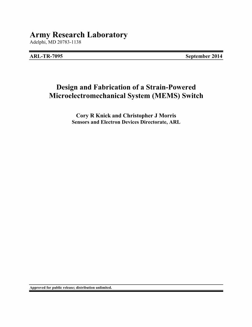
After demonstrating that wet etching was not a suitable process step, we investigated ion milling as an alternative for patterning the switch features. Therefore, in successive process iterations, we patterned the Cr and Au films through ion milling using the 4-wave 4W-PSIBE Ion Beam Etch System. Figure 8 shows an SEM of a switch patterned by ion milling. The ion milling step was superior to wet etching in several ways: 1) switch feature undercutting was not observed, 2) the Au contacts were left intact, and 3) a precise switch geometry remained after the milling. After we were able to achieve successful patterning of the switch features through ion milling, the next process step was patterning and electroplating Au frames. For this, we included an electroplate step in which a rigid Au frame between 0.25 and 4 µm thick was patterned between the hinges.
Ti Au
8
Fig. 8 SEM of switch patterned by ion milling, showing cleaner sidewalls and a well-defined switch geometry. Au contact lines are still intact, further demonstrating that ion milling is superior to wet etching. Right: switch folding after dry etch release.
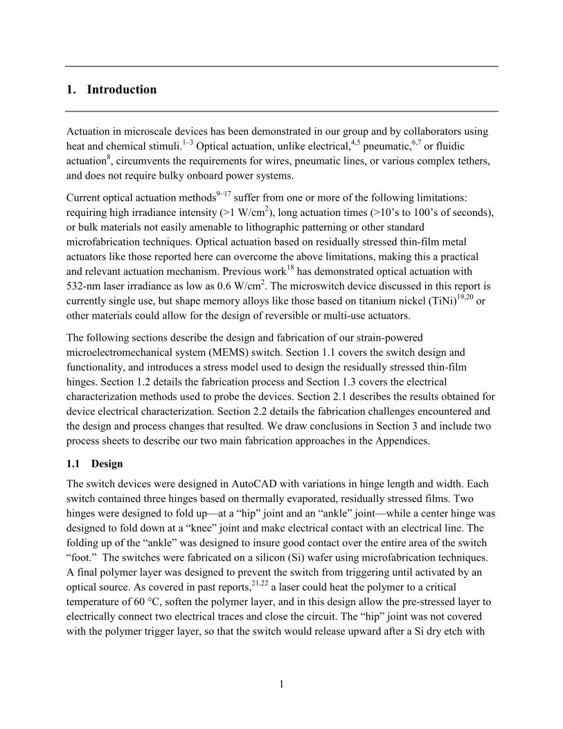
Figure 9 shows another processing challenge that we encountered. Here, test cantilevers designed to release upward after a dry etch were only partially released along the topmost edge. We determined that the second PVD evaporated layer overshot the first due to registration error, causing the cantilever to be partially anchored along this top edge. This required us to make an AutoCAD and mask design revision reducing the dimension of the second PVD step so that it did not overlap the underlying structure even with some level of error in registration between layers.
Fig. 9 Array of test cantilevers on Au contacts after dry etch release showing uniform folding upwards; the top edge appears to be anchored to the substrate, which necessitated a mask rewrite after reducing dimensions of the second PVD step

9
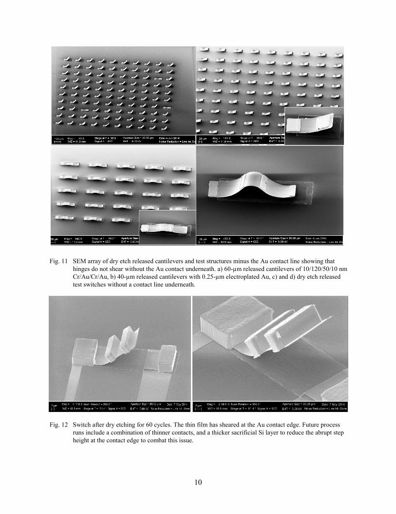
Another fabrication challenge was thin-film hinge shearing at the contact edge due to an abrupt sacrificial Si layer edge. Figure 10 shows an example of a test switch that was sheared upon dry etch release. Figure 11 shows that this shearing is not observed when Au contacts are not patterned directly beneath the switch for an array of test structures without such Au contacts since there is no longer an abrupt step height in this case. Figure 11a shows an SEM array of 60-µm cantilevers with uniform release corresponding to a metal stack of 10/120/50/10 nm Cr/Au/Cr/Au. Figure 11b shows uniform dry etch release of 40-µm cantilevers with Au electroplated on the end. The inset shows a magnified view representing the array of released switches without Au contact underneath. Figure 11c shows released SEM array of test devices without the Au contact underneath. The inset shows a higher magnification view representative of the test structure array. Figure 11d shows a single dry etch released test device exhibiting the desired folding for our residually stressed switch from the ion milling and electroplating process. Figure 12 shows a full switch that sheared upon dry etch release from the electroplating and ion milling process. To attempt to overcome this shearing issue, we reduced the Au contact thickness from 200 to 100 nm, and increased the sacrificial layer thickness to 400 nm in order to smooth out the step height profile. We also introduced quality checks to ensure that resist is developed in these regions.
Fig. 10 Problems encountered during the lift-off process run; underdeveloped resist causing the switch to be anchored (left), thin-film shearing at the contact edge (right), and thin-film edge anchoring (right). Geometry design changes were made to correct for these issues in subsequent process runs.
10
Fig. 11 SEM array of dry etch released cantilevers and test structures minus the Au contact line showing that hinges do not shear without the Au contact underneath. a) 60-µm released cantilevers of 10/120/50/10 nm Cr/Au/Cr/Au, b) 40-µm released cantilevers with 0.25-µm electroplated Au, c) and d) dry etch released test switches without a contact line underneath.
Fig. 12 Switch after dry etching for 60 cycles. The thin film has sheared at the Au contact edge. Future process runs include a combination of thinner contacts, and a thicker sacrificial Si layer to reduce the abrupt step height at the contact edge to combat this issue.
11
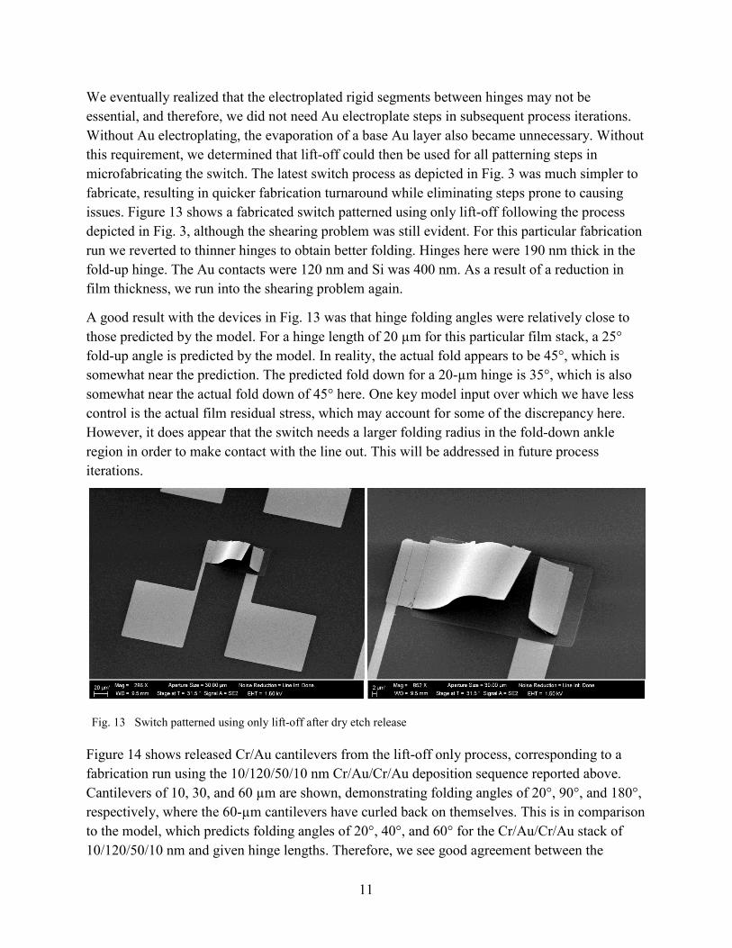
We eventually realized that the electroplated rigid segments between hinges may not be essential, and therefore, we did not need Au electroplate steps in subsequent process iterations. Without Au electroplating, the evaporation of a base Au layer also became unnecessary. Without this requirement, we determined that lift-off could then be used for all patterning steps in microfabricating the switch. The latest switch process as depicted in Fig. 3 was much simpler to fabricate, resulting in quicker fabrication turnaround while eliminating steps prone to causing issues. Figure 13 shows a fabricated switch patterned using only lift-off following the process depicted in Fig. 3, although the shearing problem was still evident. For this particular fabrication run we reverted to thinner hinges to obtain better folding. Hinges here were 190 nm thick in the fold-up hinge. The Au contacts were 120 nm and Si was 400 nm. As a result of a reduction in film thickness, we run into the shearing problem again.
A good result with the devices in Fig. 13 was that hinge folding angles were relatively close to those predicted by the model. For a hinge length of 20 µm for this particular film stack, a 25° fold-up angle is predicted by the model. In reality, the actual fold appears to be 45°, which is somewhat near the prediction. The predicted fold down for a 20-µm hinge is 35°, which is also somewhat near the actual fold down of 45° here. One key model input over which we have less control is the actual film residual stress, which may account for some of the discrepancy here. However, it does appear that the switch needs a larger folding radius in the fold-down ankle region in order to make contact with the line out. This will be addressed in future process iterations.
Fig. 13 Switch patterned using only lift-off after dry etch release
Figure 14 shows released Cr/Au cantilevers from the lift-off only process, corresponding to a fabrication run using the 10/120/50/10 nm Cr/Au/Cr/Au deposition sequence reported above. Cantilevers of 10, 30, and 60 µm are shown, demonstrating folding angles of 20°, 90°, and 180°, respectively, where the 60-µm cantilevers have curled back on themselves. This is in comparison to the model, which predicts folding angles of 20°, 40°, and 60° for the Cr/Au/Cr/Au stack of 10/120/50/10 nm and given hinge lengths. Therefore, we see good agreement between the

12
predicted fold and actual fold for this particular stack for hinges that are 20 µm or less. The agreement becomes considerably worse for hinges longer than 20 µm, with actual cantilevers folding more than predicted by the model. However, since we obtain practical folding angles with just 10–20 µm hinge lengths, there is no requirement for hinges longer than this; especially since these longer hinges have been shown to curl back onto themselves.
Fig. 14 SEM of released Cr/Au/Cr/Au cantilevers from the lift-off only fabrication run. Cantilever lengths of a) 10 µm, b) 30 µm, and c) 60 µm.
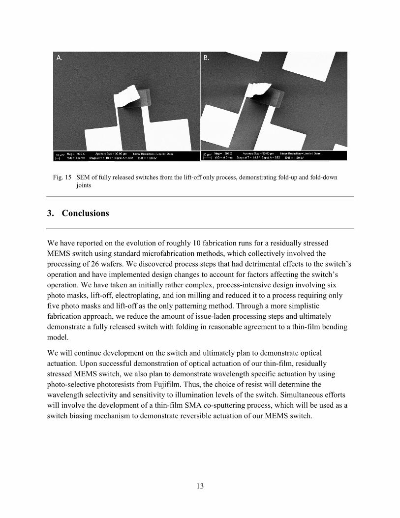
Figure 15 shows SEM images for fully released switches from the lift-off only process. Here, we were able to demonstrate both fold-up and fold-down joints, as well as a full switch with complete release. The fold-up stack for these devices is 10/120/50/10 nm Cr/Au/Cr/Au corresponding to a thin-film thickness of about 200 nm. For this process run, Au contacts were reduced from 200 nm to 100 nm and the sacrificial Si layer was 400 nm from the previous runs. This adjustment appears to have smoothed out the contact edge enough to allow for complete release of the switch. However, the fully released switch does not make contact with the line out. This switch’s 15-µm fold-up hinge creates more than enough clearance, but the 15-µm fold-down hinge does not provide enough folding to contact the line out. A longer fold-down joint or a shorter fold-up joint is likely necessary in order to close the switch. Future process runs will include fold-down hinges longer than 15 µm to obtain a larger folding radius or shorter fold-up hinges.
We also observe that when folded, switches from the lift-off only process exhibit some degree of twisting. Twisted switches were not observed for the electroplated switches, since the rigid frame only allowed the hinges to bend in one direction. In order to address the switch twisting in future process runs, we will evaporate thicker rigid Au frames in place of the electroplating step and pattern them with lift-off. We will also investigate different switch widths to help ensure that the boundary condition along the fixed edge constrains bending in one direction, rather than allowing bending in multiple directions as shown. These improvements should result in switches that fold more characteristically like those in Fig. 12, as desired.
13
Fig. 15 SEM of fully released switches from the lift-off only process, demonstrating fold-up and fold-down joints
3. Conclusions
We have reported on the evolution of roughly 10 fabrication runs for a residually stressed MEMS switch using standard microfabrication methods, which collectively involved the processing of 26 wafers. We discovered process steps that had detrimental effects to the switch’s operation and have implemented design changes to account for factors affecting the switch’s operation. We have taken an initially rather complex, process-intensive design involving six photo masks, lift-off, electroplating, and ion milling and reduced it to a process requiring only five photo masks and lift-off as the only patterning method. Through a more simplistic fabrication approach, we reduce the amount of issue-laden processing steps and ultimately demonstrate a fully released switch with folding in reasonable agreement to a thin-film bending model.
We will continue development on the switch and ultimately plan to demonstrate optical actuation. Upon successful demonstration of optical actuation of our thin-film, residually stressed MEMS switch, we also plan to demonstrate wavelength specific actuation by using photo-selective photoresists from Fujifilm. Thus, the choice of resist will determine the wavelength selectivity and sensitivity to illumination levels of the switch. Simultaneous efforts will involve the development of a thin-film SMA co-sputtering process, which will be used as a switch biasing mechanism to demonstrate reversible actuation of our MEMS switch.

14
4. References
1. Randhawa JS, Leong TG, Bassik N, Benson BR, Jochmans M. Pick-and-place using chemically actuated microgrippers. J. Am. Chem. Soc. 2008;130(51):17238–17239.
2. Morris CJ, Laflin KE, Churaman WA, Becker CR, Currano LJ, Gracias DH. Initiation of nanoporous energetic silicon by optically-triggered, residual stress powered microactuators. in Proc. 25th IEEE International Conference on MEMS, Paris, France, 2012.
3. Laflin K, Morris CJ, Bassik N, Jamal M, Gracias DH. Tetherless microgrippers with transponder tags. J. Microelectromechanical Sys. 2011;20(2):505–511.
4. Bell DJ, Lu TJ, Fleck NA, Spearing SM. MEMS actuators and sensors: observations on their performance and selection for purpose. J. MicroMech. Microeng. 2005;7(15):S153.
5. Hawkes E, An B, Benbernou NM, Tanaka H, Kim S, Demaine ED, Rus D. Programmable matter by folding. 2010;107(28):12441–12445.
6. Butefisch S, Seidemann V, Buttgenbach S. Novel micro-pneumatic Actuator for MEMS. Sens. Actuators A. 2002;97-98:638-645.
7. Hubschman J, Bourges JL, Choi W, Mozayan A, Tsirbas A, Kim CJ, Schwartz SD. A new concept of micro-forcepts for ocular robotic surgery. 2009;24:364.
8. Ninomiya T, Okayama Y, Matsumoto Y, Arouette X, Osawa K, Miki N. MEMS-based hydraulic displacement amplification mechanism with completely encapsulated liquid. 2011;166(2):277–282.
9. Ahir SV, Squires AM, Tajbakhsh AR, Terentjev EM. Infrared actuation in aligned polymer-nanotube composites. 2006;73:085420.
10. Yang L, Setyawati K, Li A, Gong S, Chen J. Reversible infrared actuation of carbon nanotube-liquid crystalline elastomer nanocomposites. Adv. Mater. 2008;20(12):2271–2275.
11. Lu S, Panchapakesan B. Nanotube micro-optomechanical actuators. Appl. Phys. Lett. 2006;88(25):253107.
12. Ikeda T, Nakano M, Yu Y, Tsutsumi O, Kanazawa A. Anisotropic bending and unbending behavior of azobenzene liquid-crystalline gels by light exposure. Avd. Mater. 2003;15(3):201–205.
13. Yu Y, Nakano M, Ikeda T. Directed bending of a polymer film by light. Nature. 2003;425:145.

15
14. Ikeda T, Mimiya J, Yu Y. Photomechanics of liquid-crystalline elastomers and other polymers. Ang. Chem. Int. Ed. 2007;46(4):506–528.
15. Liu Y, Boyles J, Genzer J, Dickey MD. Self-folding of polymer sheets using local light absorption. Soft Matter. 2012;8:1764–1769.
16. Birnbaum AJ, Pique A. Laser Induced extraplanar propulsion for three-dimensional microfabrication. Appl. Phys. Lett. 2011;98(13):134101.
17. Pique A, Mathews S, Birnbaum A, Charipar N. Microfabricating 3D structures by laser origami. SPIE Newsroom, Nov 2011.
18. Laflin K, Morris CJ, Muqeem T, Gracias DH. Laser triggered sequential folding of microstructures. Appl. Phys. Lett. 2012;101:131901.
19. Fu Y, Du H, Huang W, Zhang S, Hu M. TiNi-based thin films in MEMS applications: a review. Sens. Actuators A. 2004;112(2–3):395.
20. Gill J, Ho K, Carman G. Three-dimensional thin-film shape memory alloy microactuator with two-way effect. J. Microelectromech. Sys. 2002;11:68–77.
21. Laflin KE, Morris CJ, Muqeem T, Gracias DH. Laser triggered sequential folding of microstructures. Appl. Phys. Lett. 2012;101(131901):4.
22. Morris CJ. Modeling optical absorption for heat-induced actuation of single-use microgrippers. Adelphi (MD): US Army Research Laboratory (US); July 2012. Report No.: ARL-TR-6063.
23. Leong TG, Randall CL, Benson BR, Bassik NG, Stern M, Gracias DH. Proc. Natl. Acad. Sci. USA. 2009;106:703.
24. Nikishkov CP. J. Appl. Phys. 2003;94:5333.

16
INTENTIONALLY LEFT BLANK.

17
Appendix A. Process Sheet for Lift-Off Only Process (Wafers # 25, 26)

18
Passivate Backside 1. Acquire SSP wafers 2. VLR, PM2_ARL_SiN_ 1000A_Silane (806s) or 790 Frontside Passivation Layer 3. Deposit 200 nm SiO2 (note tool, process details) Make sure top side (without nitride) is facing up from this point forward Contacts 4. Photo 1 “Au contact v11”
a. EVG 5214 2 µm recipe (Rev) b. MA-6 Hard Contact, 20 µm gap, align to wafer _______ s exposure c. Post-Exposure Bake d. Flood expose _____ s e. Develop _______ min:s f. Rinse
Make sure thin contact lines are fully developed out at this point (left contact on each device) 5. Metroline O2 descum 2 min 6. Evatec/CHA (circle tool used)
a. Ti, 200 Å ______Å/s b. Au 1000 Å ______Å/s
7. Lift off a. acetone with light sonication b. Rinse with methanol/water
Sacrificial Si 8. Photo 2 “Sac Si v11_rev1”
a. EVG 5214 2 µm recipe (Rev) b. MA-6 Hard Contact, 20 µm gap, align to “3” _______ s exposure c. Post-Exposure Bake d. Flood expose _____ s e. Develop _______ min:s f. Rinse g. Metroline O2 descum 2 min 8. Evatec Evaporator a. 100 Å Ti b. 4000 Å Si @ 2 Å/s
(Collin Becker’s recipe should be on there) 9. Lift off
a. acetone with light sonication b. Rinse with methanol/water
Evaporate stress layers 10. Photo “Mill v11”
a. EVG 5214 2 µm recipe (Rev) b. MA-6 Hard Contact, 20 µm gap, align to “6” _______ s exposure

19
c. Post-Exposure Bake d. Flood expose _____ s e. Develop _______ min:s f. Rinse
11. Metroline O2 Descum 2-3 min 12. PVD evaporator (fold-down layer)
a. Cr, 100 Å @ 2 Å/s, 30% PWR b. Au, 1200 Å @ 4 Å/s c. Pump to at least 5e-6 Torr, and evaporate Au from source #4.
13. Lift-off a. Acetone + light sonication b. Methanol/water rinse
14. Photo 3 ”Fold Up v11” a. EVG 5214 2 um recipe b. MA-hard contact, 20 µm gap, align to “4” c. ____s expose d. Develop_____s e. Rinse f. Metroline O2 descum 2 min
15. PVD evaporator (fold-up layer) a. 500 Å Cr @ 2 Å/s, 30% PWR b. 100 Å Au @ 4 Å/s
16. Lift-off a. Acetone + light sonication b. Methanol/water rinse
Release 17. Mount wafer fragment on dicing tape to protect backside 18. Anatec asher CF4 etch to remove native silicon oxide (~15 s?) 19. XeF2, Process – STD_2t_20t_20s, 20+ cycles. Need to undercut ~20 µm 20. SEM inspection

20
INTENTIONALLY LEFT BLANK.

21
Appendix B. Process Sheet for Ion Mill and Electroplating Process

22
Passivate Backside 1. Acquire SSP wafers 2. VLR, PM2_ARL_SiN_ 1000 A _Silane (806s) or 790 Frontside Passivation Layer 3. Deposit 200 nm SiO2 (note tool, process details) Make sure top side (without nitride) is facing up from this point forward Contacts 4. Photo 1 “Au contact v11”
a. EVG 5214 2 µm recipe (Rev) b. MA-6 Hard Contact, 20 µm gap, align to wafer _______ s exposure c. Post-Exposure Bake d. Flood expose _____ s e. Develop _______ min:s f. Rinse
Make sure thin contact lines are fully developed out at this point (left contact on each device) 5. Metroline O2 descum 2 min 6. Evatec/CHA (circle tool used)
a. Ti, 200 Å ______Å/s b. Au 1000 Å ______ Å/s
7. Lift off a. acetone with light sonication b. Rinse with methanol/water
Sacrificial Si 8. Photo 2 “Sac Si v11_rev1”
a. EVG 5214 2 µm recipe (Rev) b. MA-6 Hard Contact, 20 µm gap, align to “3” _______ s exposure c. Post-Exposure Bake d. Flood expose _____ s e. Develop _______ min:s f. Rinse g. Metroline O2 descum 2 min
9. Evatec Evaporator a. 100 Å Ti b. 4000 Å Si @ 2 Å/s
10. Lift off a. acetone with light sonication b. Rinse with methanol/water
Evaporate stress layers 11. Photo “Mill v11”
a. EVG 5214 2 µm recipe (Rev) b. MA-6 Hard Contact, 20 µm gap, align to “6” _______ s exposure c. Post-Exposure Bake d. Flood expose _____ s

23
e. Develop _______ min:s f. Rinse
12. Metroline O2 Descum 2-3 min 13. PVD evaporator (fold-down layer)
a. Cr, 100 Å @ 2 Å/s, 30% PWR b. Au, 1200 Å @ 4 Å/s c. Pump to at least 5e-6 Torr, and evaporate Au from source #4.
14. Lift-off a. Acetone + light sonication b. Methanol/water rinse
15. Photo 3 ”Fold Up v11” a. EVG 5214 2 µm recipe b. MA-hard contact, 20um gap, align to “4” c. ____s expose d. Develop_____sec e. Rinse f. Metroline O2 descum 2 min
16. PVD evaporator (fold-up layer) a. 500 Å Cr @ 2 Å/s, 30% PWR b. 100 Å Au @ 4 Å/s
17. Lift-off a. Acetone + light sonication b. Methanol/water rinse
Release 18. Mount wafer fragment on dicing tape to protect backside 19. Anatec asher CF4 etch to remove native silicon oxide (~15 s?) 20. XeF2, Process – STD_2t_20t_20s, 20+ cycles. Need to undercut ~20 um 21. SEM inspection

24
List of Symbols, Abbreviations, and Acronyms
Au gold
Cr chromium
DI deionized
MEMS microelectromechanical system
PVD physical vapor deposition
SEM scanning electron microscopy
Si silicon
TiNi titanium nickel
XeF2 xenon difluoride

25
1 DEFENSE TECHNICAL (PDF) INFORMATION CTR DTIC OCA 2 DIRECTOR (PDF) US ARMY RESEARCH LAB RDRL CIO LL IMAL HRA 1 GOVT PRNTG OFC (PDF) A MALHOTRA 2 DIRECTOR (PDF) US ARMY RESEARCH LAB RDRL SES L CORY R KNICK CHRISTOPHER J MORRIS

26
INTENTIONALLY LEFT BLANK.