
Design a Bandpass Filter for GSM 900 - DiVA portal655239/FULLTEXT01.pdf · Bo Liu Design a Bandpass...
43
FACULTY OF ENGINEERING AND SUSTAINABLE DEVELOPMENT . Design a Bandpass Filter for GSM 900 Half Wavelength Open Circuit Stubs Filter Design Bo Liu Feb. 2013 Thesis Paper in Electronics and Telecomunications Examiner: Prof. Jose Chilo
Transcript of Design a Bandpass Filter for GSM 900 - DiVA portal655239/FULLTEXT01.pdf · Bo Liu Design a Bandpass...

FACULTY OF ENGINEERING AND SUSTAINABLE DEVELOPMENT .
Design a Bandpass Filter for GSM 900
Half Wavelength Open Circuit Stubs Filter Design
Bo Liu
Feb. 2013
Thesis Paper in Electronics and Telecomunications
Examiner: Prof. Jose Chilo

Bo Liu Design a Bandpass Filter for GSM 900
i
Abstract
Microstrip is a technology to manufacture filters, antennas, couplers and other electronics
elements used in communication systems. This technology plays an important role in radio
system and microwave applications. For the low cost, small size and easy design and
implementation, microstrip is widely used in elements of RF communication system,
especially for the case of filter. Filter is usually used together with high power amplifier in
order to guarantee the performance of the RF communication system. However, it is difficult
to find a suitable filter for special radio system. Since such filters are always capable of
handling high power with compacted harmonic suppression. The difficulties become even
more when constraint on phase linearity is put on the filter.
In this thesis work, we have designed, simulated and manufactured a high power, low return
loss, microstrip bandpass filter. The frequency range of the filter is 900- 1000MHz. We use
200W RMS power and 800W peak power with 0.1dB ripple in passband to process on the
filter. Moreover the suppression of 2nd
and 3rd
harmonics is at least 20dB.
We investigated on two kinds of methods to design the filter: (1) parallel coupling filter, (2)
filters with half-wavelength open-circuited stubs. The reason why we chose these two kinds
of methods is because their planar structure, easy design and implementation in the laboratory.
Simulations are processed on Advanced Design System (ADS). Simulation results show that
filters with half-wavelength open-circuited stubs has almost the same performance compared
with parallel coupling filter. And parallel coupling filter has better performance at the 2nd
and
3rd
harmonics. However the power handling capability of the filter with half-wavelength
open-circuited stubs is much higher. Thus the filter with half-wavelength open-circuited stubs
was chosen to manufacture.
Simulations are based on the substrate duroid RT6035HTC for the high thermal conductivity,
low loss tangent and thermally stable low profile. The calculations of the average power
handling capability (APHC) and peak power handling capability (PPHC) are also shown
before manufacturing in order to theoretically verify the feasibility of design at such high
power.

Bo Liu Design a Bandpass Filter for GSM 900
ii
For the filter with half-wavelength open-circuited stubs, reductions of the 2nd
and 3rd
harmonics are achieved by replacing the quarter-wavelength connecting lines to equivalent T-
shaped transmission line. Besides, optimization of the dimensions is also processed on ADS.

Bo Liu Design a Bandpass Filter for GSM 900
iii
CONTENTS
Abstract .................................................................................................................................................... i
CONTENTS ........................................................................................................................................... iii
LIST OF FIGURE ................................................................................................................................... v
LIST OF TABLE .................................................................................................................................... v
1 INTRODUCTION ........................................................................................................................... 1
1.1 Topic Introduction ..................................................................................... 错误!未定义书签。
1.2 Goal .......................................................................................................................................... 1
1.3 Method ..................................................................................................................................... 2
1.4 Outline ...................................................................................................................................... 2
2 THEORY ......................................................................................................................................... 3
2.1 Theory of Microstrip Transmission Line ................................................................................. 3
2.1.1 Microstrip Transmission Line .......................................................................................... 3
2.1.2 Microstrip Open End ........................................................................................................ 6
2.2 Theories of microstrip Filters ................................................................................................... 7
2.2.1 Transfer Functions ............................................................................................................ 7
2.2.2 The Poles and Zeros on the Complex Plane ..................................................................... 8
2.2.3 Chebyshev Response ........................................................................................................ 8
2.2.4 Chebyshev Lowpass Prototype Filters and Elements ..................................................... 10
2.3 Half wavelength open-circuit stubs bandpass filters .............................................................. 12
2.4 Equivalent T-shaped Transmission Line ................................................................................ 14
2.5 Average Power Handling Capability (APHC) ....................................................................... 15
3 PROCESS AND RESULTS .......................................................................................................... 18
3.1 Implementation Setup ............................................................................................................ 18
3.2 Choose Substrate .................................................................................................................... 19
3.3 Filter Design ........................................................................................................................... 20
3.4 Simulation .............................................................................................................................. 22

Bo Liu Design a Bandpass Filter for GSM 900
iv
3.5 Comparison and Analysis ...................................................................................................... 23
3.6 Suppression of 2nd
, 3rd
Harmonic and Results ........................................................................ 23
3.7 Manufacture and Results ........................................................................................................ 26
3.7.1 Calculation of Power Handling Capability of the Design .............................................. 26
3.7.2 Manufacture .................................................................................................................... 27
3.7.3 Measurement Results and Analysis ................................................... 错误!未定义书签。
3.8 Discussion .............................................................................................................................. 29
4 CONCLUSION ............................................................................................................................. 31
REFERENCES ...................................................................................................................................... 32
APPENDIX - MATLAB SCRIPT OF THE DESIGN EQUATION .................................................... 34

Bo Liu Design a Bandpass Filter for GSM 900
v
LIST OF FIGURE
Figure 1: Physical structure of microstrip transmission line
Figure 2: Electric and magnetic field lines of microstrip transmission line
Figure 3: Approximated geometry of the microstrip line
Figure 4: Compensation for the microstrip open end
Figure 5: Chebyshev lowpass response
Figure 6: Pole distribution of Chebyshev response
Figure 7: Two type of lowpass prototype filter
Figure 8: Transmission line bandpass filter with quarter-wavelength short-circuited stubs.
Figure 9: Transmission line bandpass filter with half-wavelength open-circuited stubs.
Figure 10: Series connecting line (left) and equivalent T-shaped transmission line (right).
Figure 11: Cross-section of microstrip line in multilayer laminate
Figure 12: Flow chart of the design process
Figure 13: Frequency response (a) and phase response in passband (b)
Figure 14: Layout of the filter design
Figure 15: Frequency response (a) and phase response (b) after processing harmonics suppression
Figure 16: Designed filter with connectors
Figure 17: Frequency response (a) and phase response (b) of the filter
Figure 18: Comparison for final results and theoretical results

Bo Liu Design a Bandpass Filter for GSM 900
vi
LIST OF TABLE
Table 1: Specification of the bandpass filter
Table 2: Datasheet for RO4003 and RT6035 HTC
Table 3: Element values of 5th order Chebyshev lowpass prototype with 0.1ripples
Table 4: Design parameters of the filter
Table 5: Dimensions of the equivalent T-Shaped transmission lines
Table 6: Dimensions for the microstrip lines of the filter
Table 7: Calculation results of APHC of the filter

Bo Liu Design a Bandpass Filter for GSM 900
1
1 INTRODUCTION
1.1 Backgrounds
In RF communication systems, amplifier is one of the most important elements. High quality
amplifier is the security of the communication system performance. And a bandpass filter is
an important component, usually used together with power amplifier at the transmitter or
receiver in radio system. It is the element used to verify the performance of amplifiers.
Bandpass filters are passive components which are able to select signals in a specific
bandwidth and reject signals in another frequency range. When filtering the signal from the
amplifier, it’s very important to keep the accuracy of the signal, otherwise the signal will be
distorted. However it is not an easy work to find a suitable filter for special amplifier. The
difficulties become even more when constraint high power handling capability, harmonic
suppression and the phase linearity on the filter. [1]
Normally, the structures of high power filter are fulfilled as cavity and High Temperature
Superconductor (HTS) microstrip. However, cavity filter is too larger in size and the material
of HTS microstrip is too expensive. As alternative, microstrip filter based on printed circuit
board (PCB) offers the advantages easy and cheap in mass production. But it has the
disadvantages of higher insertion losses and wider transition region.
1.2 Goal
The goal of this thesis to design and construct a high power bandpass filter for GSM900 based
on PCB microstrip technology which is supported by University of Gavle. The filter should
be linearly worked on the frequency range of 900MHz to 1000MHz with the RMS power of
200W and peak power of 800W. The insertion loss of the filter is less than 1dB with the
ripple of 0.1dB and return loss in passband is better than 20dB. And the suppression of 2nd
and 3rd
harmonics should be at least 20dB.

Bo Liu Design a Bandpass Filter for GSM 900
2
1.3 Method
In realization of such a bandpass filter, the main questions we faced are the very low insertion
loss in passband with extreme high operation power, the suppression of the 2nd
and 3rd
harmonics, and the linearity of the phase response.
In order to fulfill these requirements there are several strategies taken in realization of the
filter, such as, the choice of microstrip filter technology based on PCB is preferred in respect
to the advantages easy and cheap in mass production, select Rogers RT6035HTC PCB
laminate to manufacture the filter for its low loss tangent and high temperature tolerance and
stability of ceramics substrate [2], and the use of equivalent T-shaped connecting lines on
account of the frequency response at the harmonics and the fundamental frequency [1] [3],
Etc.
In this thesis, each of us will investigate and simulate one type of microstrip filter on ADS (or
HFSS) separately, choose one of them by comparing the performances and the characteristics,
then fabricate it in the laboratory of University of Gavle. After that we will process the
performance measurement to verify if the design is survive or not.
1.4 Outline
These outlines briefly describe the main part of this thesis:
Theory: the basic knowledge for microstrip line, microstrip filter will be demonstrated.
Overview the method of design half wavelength open-circuit stubs filter and coupled line
filter.
Implementation and analysis: simulate the filters by using ADS software and manufacture
the filter and measure it.
Conclusion: thesis conclusion
Bo Liu Design a Bandpass Filter for GSM 900
3
2 THEORY
In this section, we will discuss the characteristic of the microstrip line and analysis how to
design a microstrip, describe the theory of microstrip filter, discuss the type of filter used in
the designing part, for this part half wavelength open-circuit stubs bandpass filters are
introduced. Then we describe the method used to overcome the 2nd
and 3rd
harmonics, and a
mathematical method to approximately calculate the average power handling capability of the
microstrip line.
2.1 Theory of Microstrip Transmission Line
Microstrip transmission line is one of the most commonly used transmission lines in Radio
frequency applications [1].The planar configuration of it can be achieved by several ways,
such as with the photolithography process or thin-film and thick film technology. It can be
exploited for designing both passive and active microwave circuits, like filter, coupler, or
power divider.
2.1.1 Microstrip Transmission Line
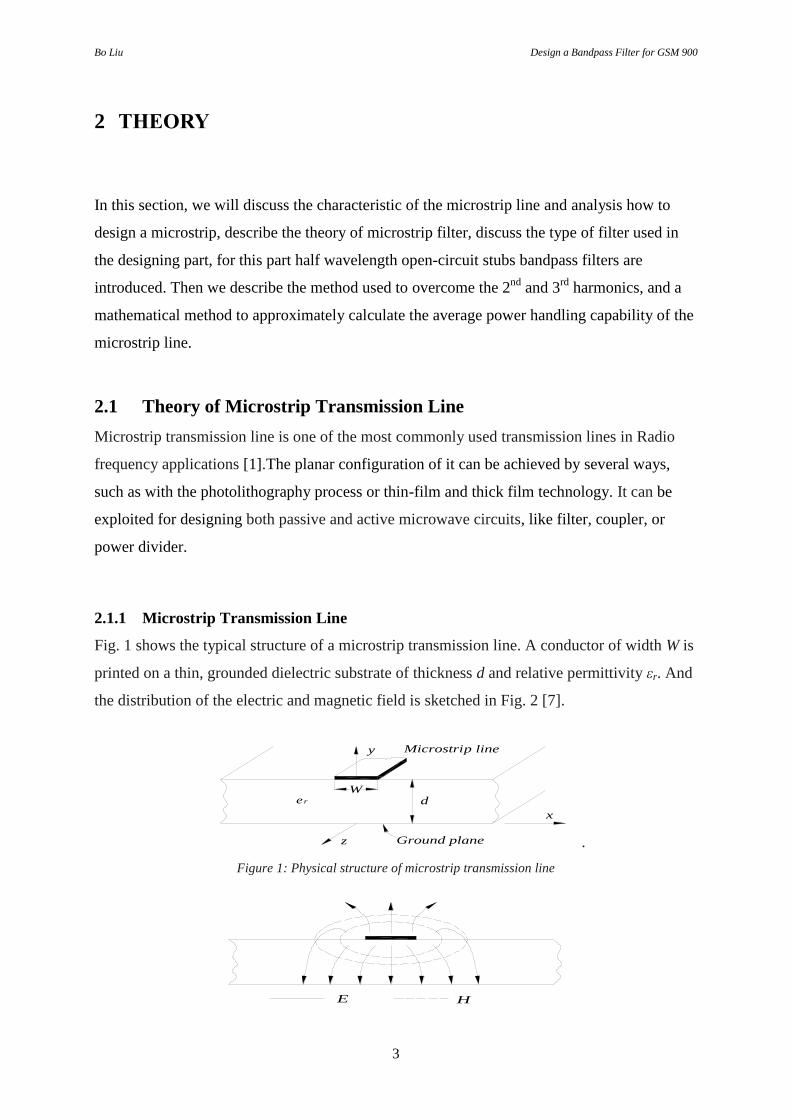
Fig. 1 shows the typical structure of a microstrip transmission line. A conductor of width W is
printed on a thin, grounded dielectric substrate of thickness d and relative permittivity εr. And
the distribution of the electric and magnetic field is sketched in Fig. 2 [7].
We r d
z
x
y
Ground plane
Microstrip line
.
Figure 1: Physical structure of microstrip transmission line
E H

Bo Liu Design a Bandpass Filter for GSM 900
4
Figure 2: Electric and magnetic field lines of microstrip transmission line
When the grounded dielectric substrate has dielectric constant of 1(εr = 1), the strip conduct
and the ground plane are embedded in a homogeneous medium (air). This simple case
constitute a TEM transmission line with phase velocity vp equal to c (speed of the light in free
space) and propagation constant β = k0. [8]
If the dielectric constant of the substrate would not equal to 1(εr ≠ 1), the behavior of the
microstrip line is much more complicate. Most of its field lines are existing in the dielectric
region between the strip conductor and the ground plane and some fraction in the air region
above the substrate. [9] Therefore the field of microstrip line is not a pure TEM wave.
Because the phase velocity of TEM fields in the dielectric region would be √ , while the
phase velocity of TEM fields in the air region would be c. So it would be impossible to
achieve a phase-matching condition at the dielectric–air interface. [10]
In actuality, the exact fields of a microstrip line constitute a hybrid TM-TE wave and require
more advanced techniques to analysis. In most practical applications, the dielectric substrate
is very thin ( ), and the fields are so called quasi-TEM. i.e., the fields are essentially the
same as those of the static (DC) case. [11] Then the phase velocity and propagation constant
can be obtained from quasi-static solutions
√ (1)
√ (2)
where εe is the effective dielectric constant of the microstrip line. The effective dielectric
constant satisfies the relation 1 < εe < εr. And the effective dielectric constant is also depends
on the substrate dielectric constant, the substrate thickness, the conductor width, and the
cutoff frequency.
The effective dielectric constant of a microstrip line is given approximately by [9]
√ ⁄ (3)
W is the width of the microstrip line, d is the thickness of the substrate, is the dielectric
constant of the substrate. The effective dielectric constant can be interpreted as the dielectric

Bo Liu Design a Bandpass Filter for GSM 900
5
constant of a homogeneous medium that equivalently replaces the air and dielectric regions of
the microstrip line, as shown in Fig. 3.
We r d
Ground plane
Microstrip lineee
d
Microstrip line
Figure 3: Approximated geometry of the microstrip line
Given the dimensions of the microstrip line, the characteristic impedance can be calculated as
{
√
⁄
√ ⁄ ⁄ ⁄
(4)
For a given characteristic impedance Z0 and dielectric constant εr , the W/d ratio can be found
as
{
⁄
[
{
}] ⁄
(5)
where
√
√
Considering a microstrip line as a quasi-TEM line, we can determine the attenuation due to
dielectric loss as [10]
⁄ (6)
which means the fields around the microstrip line are partly in air (lossless) and partly in the
dielectric (lossy).
The attenuation due to conductor loss is given approximately by [11]

Bo Liu Design a Bandpass Filter for GSM 900
6
⁄ (7)
where √ ⁄ is the surface resistivity of the conductor. For most microstrip
substrates, conductor loss is more significant than dielectric loss. However, exceptions may
occur with some semiconductor substrates.
The results of effective dielectric constant, characteristic impedance, and attenuation of
microstrip line are curve-fit approximations to rigorous quasi-static solutions [12].
2.1.2 Microstrip Open End
Due to the fringing field effect, the fields slightly extend further rather than abruptly stop at
the open end of the microstrip line [12]. This phenomenal can be modeled with an equivalent
length of transmission line shown in Fig. 4. And a closed-form expression for calculating the
equivalent length is given by [13]
T T
l
Figure 4: Compensation for the microstrip open end
(8)
where
⁄
⁄
(9)
⁄
(10)
⁄ ⁄
(11)
⁄ (12)

Bo Liu Design a Bandpass Filter for GSM 900
7
⁄ (13)
2.2 Theories of microstrip Filters
Microstrip filters are the one of most widely used filters in RF communication system. It has
the advantages of easy and cheap in mass production. But it also has the disadvantages of
higher insertion losses and wider transition region.
2.2.1 Transfer Functions
The transfer function of a filter is a mathematical expression of the transmission (S21) of the
two-port network. And the transfer function depicts the response characteristics of the filter
response [12]. Normally, the transfer function is defined as the amplitude-squared of the
transmission, which is
| |
(14)
where is a ripple constant, is a characteristic function, and is a frequency variable
in radian frequency. For a lowpass prototype filter that has a cutoff frequency at for
.
For linear, time-invariant networks, the transfer function may be defined as a rational function,
that is
(15)
where N(p) and D(p) are polynomials in a complex frequency variable p = σ+ jΩ. In many
cases, the rational transfer function can be constructed from the amplitude squared transfer
function [1–2].
For a given amplitude-squared transfer function, the insertion loss of the filter can be
computed by
| | (16)

Bo Liu Design a Bandpass Filter for GSM 900
8
Since | | | |
for a lossless, passive two-port network, the return loss of the filter
can be found by using
| | (17)
If a rational transfer function is available, the phase response of the filter can be found as
(18)
Then the group delay response of this network can be calculated by
(19)
where is in radians and Ω is in radians per second [12].
2.2.2 The Poles and Zeros on the Complex Plane
For a rational transfer function, the complex plane is at which the function is defined, and it
also called the (σ, Ω) plane or p-plane. The horizontal axis is called the real or σ-axis, and the
vertical axis is called the imaginary or jΩ-axis.
The zeros of the function are the values of p at which the function becomes zero, and the
poles are the values of p at which the function becomes infinite. Therefore, the zeros of S21(p)
are the roots of the numerator N(p) and the poles of S21(p) are the roots of denominator D(p).
The poles of a rational transfer function will be the natural frequencies of the filter. For the
stability of the filter, these natural frequencies must lie in the left half of the complex plane, or
on the jΩ-axis. Otherwise, oscillations would be of exponentially increasing in magnitude
with respect to time, which is impossible in a passive network. Hence, D(p) is a Hurwitz
polynomial [3]; i.e., its roots are in the left half-plane, or on the jΩ-axis, whereas the roots of
N(p) may occur anywhere on the entire complex plane. The roots of N(p) are called finite-
frequency transmission zeros of the filter [12].
2.2.3 Chebyshev Response
Fig. 7 shows a Chebyshev response, which has equal-ripple in passband and maximally flat in
stopband. The amplitude-squared transfer function of Chebyshev response is

Bo Liu Design a Bandpass Filter for GSM 900
9
| |
(20)
where ε is the ripple constant and it is related to passband ripple LAr in dB by
√ (21)
Tn(Ω) is a Chebyshev function given by
{ | |
| | (22)
Ω
LA(d
B)
Ωc
LAr
Figure 5: Chebyshev lowpass response
The general formula of the rational transfer function for the Chebyshev filter is
∏ ⁄ ⁄
∏
(23)
where
The pole locations for the Chebyshev response lie on an ellipse in the left half-plane. The

Bo Liu Design a Bandpass Filter for GSM 900
10
j(1+ η^2)^(0.5)
-j(1+η^2)^(0.5)
n = 5
σ-η
j Ω
Figure 6: Pole distribution of Chebyshev response
major axis of the ellipse is on the jΩ-axis with size of √ ; the minor axis is on the -
axis of size . Fig. 8 shows a pole distribution of Chebyshev response for n = 5 [12].
2.2.4 Chebyshev Lowpass Prototype Filters and Elements
A Chebyshev lowpass prototype filter is defined as the Chebyshev lowpass filter whose
element values are normalized to make the source resistance or conductance equal to one,
denoted by g0 = 1, and the cutoff angular frequency to be unity, denoted by Ωc =1(rad/s). Fig.
9 demonstrates two possible forms of an n-pole lowpass prototype for realizing a Chebyshev
filter response. Either form may be used because both are dual from each other and give the
same response. n is the number of reactive elements. [11]
g0 g1
g2
g3
gn
gn+1 gnor
n even n odd
gn+1
g0 gn
gn
or
n even n odd
g2
g1 g3
gn+1 gn+1
Figure 7: Two type of lowpass prototype filter

Bo Liu Design a Bandpass Filter for GSM 900
11
This type of lowpass filter can serve as a prototype for designing many practical filters with
frequency and element transformations.
For Chebyshev lowpass prototype filters with a passband ripple LAr dB and the cutoff
frequency Ωc = 1, the element values for the two-port networks may be given by
(24)
(25)
(26)
{
(
)
(27)
where
[ (
)]
For a given passband ripple LAr dB and the minimum stopband attenuation LAs dB at Ω = Ωs,
the degree of a Chebyshev lowpass prototype may be found as
√
(28)
Sometimes, the minimum return loss LR or the maximum voltage standing wave ratio VSWR
in the passband is specified instead of the passband ripple LAr. If the return loss is defined and
the minimum passband return loss is LR dB (LR < 0), the corresponding passband ripple is
calculated as [11]
(29)
Since the VSWR is defined as
| |
| | (30)

Bo Liu Design a Bandpass Filter for GSM 900
12
When the VSWR is specified, the passband ripple LAr is given by
[ (
)
] (31)
2.3 Half wavelength open-circuit stubs bandpass filters
Fig. 8 shows a so called stub bandpass filter that is comprised of quarter-wavelength shunt
short-circuit stub with quarter-wavelength connecting lines. The characteristic admittances of
shunt stubs and the connecting lines determine the characteristic of the stub bandpass filter.
For an n degree filter, the design equations are given by [14]
ln
short-citcuit stub
ln-1,n
Y 1,2 Y n-1,nY 0 Y 0
Y 1 Y 2 Y nY n-1
l1,2
l1
Figure 8: Transmission line bandpass filter with quarter-wavelength short-circuited stubs.
(
) (32)
√ ; (33)
√
(34)
√
(35)
√ (36)
√
(37)
(
) (
) (38)
Bo Liu Design a Bandpass Filter for GSM 900
13
(
) (
) (39)
(
) (40)
(
) (41)
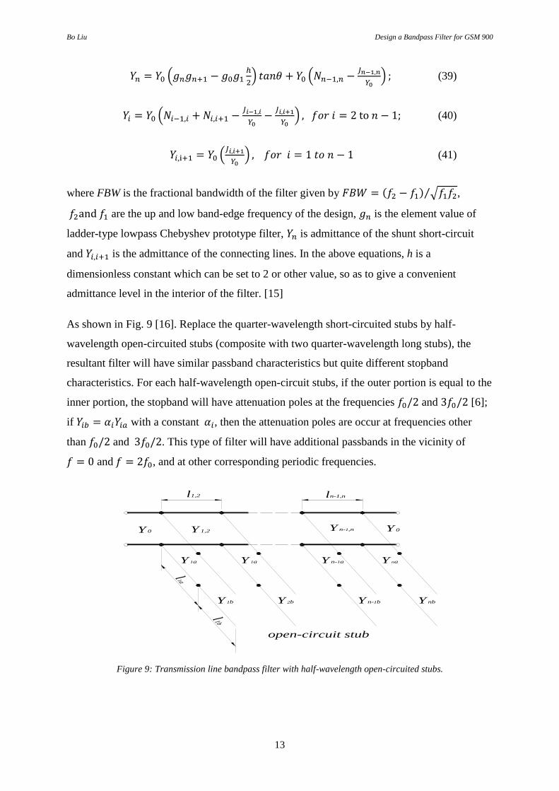
where FBW is the fractional bandwidth of the filter given by √ ⁄ ,
are the up and low band-edge frequency of the design, is the element value of
ladder-type lowpass Chebyshev prototype filter, is admittance of the shunt short-circuit
and is the admittance of the connecting lines. In the above equations, h is a
dimensionless constant which can be set to 2 or other value, so as to give a convenient
admittance level in the interior of the filter. [15]
As shown in Fig. 9 [16]. Replace the quarter-wavelength short-circuited stubs by half-
wavelength open-circuited stubs (composite with two quarter-wavelength long stubs), the
resultant filter will have similar passband characteristics but quite different stopband
characteristics. For each half-wavelength open-circuit stubs, if the outer portion is equal to the
inner portion, the stopband will have attenuation poles at the frequencies and [6];
if with a constant , then the attenuation poles are occur at frequencies other
than and . This type of filter will have additional passbands in the vicinity of
and , and at other corresponding periodic frequencies.
l1a
l1b
open-circuit stub
l1,2 ln-1,n
Y 0 Y 1,2 Y n-1,n Y 0
Y 1a Y 1a Y n-1a Y na
Y 1b Y 2b Y n-1b Y nb
Figure 9: Transmission line bandpass filter with half-wavelength open-circuited stubs.

Bo Liu Design a Bandpass Filter for GSM 900
14
The design of this type of filter can use the modification of the design equations of quarter-
wavelength short-circuit stubs filter described before. Firstly, give a filter in the form in Fig.
10 with the desired characteristics. Then replace the quarter-wavelength short-circuit stub by a
shunt half-wavelength, open-circuited stub which have an inner quarter-wavelength portion
with a characteristic admittance
(42)
and outer portion with a characteristic admittance
(43)
where is given by
(
) (44)
where is a frequency at which the shunt open-circuited stub presents a short circuit to the
main transmission line and causes a transmission zero or attenuation pole [9].
2.4 Equivalent T-shaped Transmission Line
By replacing the series quarter-wavelength connecting lines of the filters with the equivalent
T-shaped lines, it could have compact half-wavelength open-stub bandpass filters with
harmonics suppression [6]. The T-shaped transmission line works like a bandstop filter at the
harmonics by choosing different electric length and impedance of T-shaped branches. The
electric length and the impedance of the three branches are derived from analyzing the ABCD
matrix of the transmission lines. Fig. 10 shows a typical quarter-wavelength connecting line
with the equivalent T-shaped connecting line.[15]
Z1 θ1
Z2 θ2 Z2 θ2
Z3
θ3
Figure 10: Series connecting line (left) and equivalent T-shaped transmission line (right).
The ABCD matrix of the original quarter-wavelength connecting line is given by [15]

Bo Liu Design a Bandpass Filter for GSM 900
15
[
] (45)
The equivalent T-shaped connecting line is combined with two equivalent series-stubs and a
shunt-stub as shown in Fig. 10. And the ABCD matrix of is given by
(46)
where
[
] [
] (47)
Since the T-shaped line is used to replace the series quarter-wavelength connecting line, is
assigned to 90°.When the T-shaped line is designed to suppress the nth
order harmonic, is
assigned to be at . Because at the nth
order harmonic the electrical length of the shunt
stub would be 90°, thus the T-shaped line shows a transmission zero at the nth
harmonic. The
shunt stub works like a BSF to suppress the harmonics. should be greater than 0° and less
than 45°. When is tend to 45°, the impedance looking into the shunt stub goes to infinity.
Thus the shunt stub acts as an open circuit and could be neglected. And the T-shaped line
becomes the original connecting transmission line.
Equating (46) (47) yields [16]
(48)
and
(49)
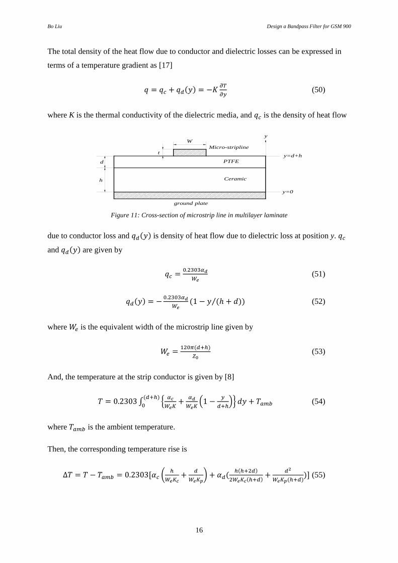
2.5 Average Power Handling Capability (APHC)
The APHC of a multilayer microstrip is determined by the temperature rise of the strip
conductor and the supporting dielectric layers and the substrate. In other words, it is related to
the loss tangent and thermal conductivity of the substrate. A cross-section of the RT6035 PCB
laminate is shown in Fig. 14.
Bo Liu Design a Bandpass Filter for GSM 900
16
The total density of the heat flow due to conductor and dielectric losses can be expressed in
terms of a temperature gradient as [17]
(50)
where K is the thermal conductivity of the dielectric media, and is the density of heat flow
ground plate
Ceramic
PTFE
Micro-striplinet
d
h
W
y=0
y
y=d+h
Figure 11: Cross-section of microstrip line in multilayer laminate
due to conductor loss and is density of heat flow due to dielectric loss at position y.
and are given by
(51)
⁄ (52)
where is the equivalent width of the microstrip line given by
(53)
And, the temperature at the strip conductor is given by [8]
∫ {
(
)}
(54)
where is the ambient temperature.
Then, the corresponding temperature rise is
(
)
(55)

Bo Liu Design a Bandpass Filter for GSM 900
17
where and are the thermal conductivities of the ceramic substrate and PTFE layer,
respectively.
Thus the power handling capability of the microstrip line is
(56)
where Tmax is the maximum temperature that the microstrip line can stand.

Bo Liu Design a Bandpass Filter for GSM 900
18
3 PROCESS AND RESULTS
In this section, the filter design process will be presented. In order to achieve a better
performance of the filter, each of us will investigate and design a different type of microstrip
filter in the beginning, and we choose one to bring about the fabrication. Then process the
measurement of the filter. After that we will discuss the differences between the actual result
and the simulated result.
3.1 Implementation Setup
The filter design is begins with choosing a suitable substrate. Since the operation power of the
required filter is extremely high, a good substrate with low loss and endurance of high
temperature is the guarantee of the design. Then each of us will design and simulate one type
of microstrip filter: half-wavelength open-circuited stubs filter and parallel-coupled line filter.
The main reasons why we choose this two type of microstrip filters are their linear response in
passband, planar structure, and easy and cheap in fabrication. And the simulation is done on
ADS. Here in this paper only the design of half-wavelength open-circuited stubs filter is
presented, and my partner Che Liu will present the process of designing parallel-coupled line
filter. By comparing the simulation results of the two filters, we will choose a more suitable
one to bring about manufacture. In order to fulfill the requirement on harmonics, optimization
on the transmission line and a method called equivalent T-shaped transmission line are used
to combat the 2nd
and 3rd
harmonics before the filter goes to manufacture. Then process the
measurement of the filter to verify if the performance agree with the theoretical results and
simulation or not. The process is briefly shown in the Fig.12.

Bo Liu Design a Bandpass Filter for GSM 900
19
Figure 12: Flow chart of the design process
3.2 Choose Substrate
The filter design should be follow the specification which is shown in Table 1:
Table 1: Specification of the bandpass filter
Power 200W RMS and 800W Peak Power
Insertion loss Less than 1dB
Return loss in passband Better than 20dB
Phase Linear
Ripples in passband 0.1dB
Passband 900MHz to 1000MHz
Suppression of 2nd and 3rd harmonics At least 20dB

Bo Liu Design a Bandpass Filter for GSM 900
20
As mentioned in the Table 1, the power levels of the filer are RMS of 200W and peak power
of 800W. Thus the design will require substrate with low loss tangent. Because loss tangent is
the main factor of influence the power handling capability for PCB [17]. Besides 1 dB
insertion loss of 200 W corresponds to 41 W, it means there has 41W power dissipated in the
filter. Thus we need the substrate with high thermal conductivity, and the design width of the
conductors cannot be too narrow or they will melt.
In short, substrates with low loss tangent and large thermal conductivity will suitable for the
design. By comparing the data sheets of PCB laminates provided by Rogers Corp., two type
of PCB laminate, RO4003 and RT6035 HTC, are to be considered, because the material of
their substrate are ceramic. Ceramic substrate makes these two kinds of PCB laminate more
temperature tolerable and more stable at high temperature. And the main parameters of the
two type of laminate are list in Table 2.
Table 2: Datasheet for RO4003 and RT6035 HTC
parameters RO4003 RT6035 HTC
loss tangent 0.0027 0.0013
thermal conductivity 0.64 1.44
Dielectric constant 3.55 3.6
Thermal coefficient of εr. 40 -66
Permittivity 10 10
Thickness 1.524 mm 1.524 mm
Coefficient of thermal expansion 46 (z direction) 39 (z direction)
Comparing the data given in Table 2, the two type of PCB laminate have almost the same
parameters. But the RT6035 HTC has lower loss tangent, coefficient of thermal expansion
and higher thermal conductivity. This makes it more safety for this case. Thus we choose
RT6035 HTC to fulfill the design process.
3.3 Filter Design
In this part, only the method of half-wavelength open-circuited stubs filter will be present. My
partner Che Liu will present the method of parallel-coupled line filter.
According to the theory of Chebyshev lowpass prototype filter mentioned before, for 20 dB
return loss with 0.1 dB ripples in passband, the 4th
order filter is appropriate for the design

Bo Liu Design a Bandpass Filter for GSM 900
21
requirement [17]. But here we would like to choose the 5th
order for the symmetry structure
and higher power handling capability. Table. 3 illustrate the element values which are
obtained by applying the Eq. (24) to (27).
Table 3: Element values of 5th
order Chebyshev lowpass prototype with 0.1ripples
g0 g1 g2 g3 g4 g5 g6
1 1.1468 1.3712 1.975 1.3712 1.1468 1
The bandpass filter is designed to operate from the frequency range of 900 MHz to 1000 MHz,
which corresponds to have a fractional bandwidth FBW = 0.105. And the impedance of the
terminal line is chosen to be 50 ohm, which gives Y0 = 1/50 mhos. Applying the microstrip
design equations described in theory part, the widths and guided quarter-wavelengths
associated with the characteristic admittances can be calculated. And the results are
summarized in Table. 4. Here in this design,
(
) and
which leads to (
) in Eq. (44).
By considering the fringe effect, compensation for the open end of the open-circuited stubs
must be taken into account. Using the design equation described in equation 8 to 13, the
dimensions of the equivalent line length of microstrip open end are calculated. The results are
list in Table 5.
Thus the total lengths of the open-circuited stubs are computed according to the following
equation:
(57)
where li are the lengths of the open-circuited stubs.
Table 4: Design parameters of the filter
i
1
2

Bo Liu Design a Bandpass Filter for GSM 900
22
3
4
5
- - -
Table 5: Design parameters of the filter by considering the compensation of fringe effect
Stubs
81.3 0.6548 2.5957 0.5626
40.8163 3.0243 2.8833 0.8082
40.9836 3.0061 2.8819 0.8063
40.8163 3.0243 2.8833 0.8082
81.3 0.6548 2.5957 0.5626
3.4 Simulation
The simulation work of the design is achieved on ADS. Using the design parameters given in
Table 4 and 5 associated with equation .., the schematic diagram is built on ADS. Fig. 13(a)
plots the filter frequency response obtained by EM simulations. Generally after optimization,
the insertion loss, bandwidth and passband ripples are agreement with the design requirement.
But the passband slightly larger than the theoretical value and the return loss is higher than the
expect value. It also can be seen that, the filter has a 2nd
and 3rd
passband around and
which should be defeated in the following procedure. The phase response of the filter is
almost linear in the passband which is shown in Fig. 13(b).

Bo Liu Design a Bandpass Filter for GSM 900
23
(a)
(b)
Figure 13: Frequency response (a) and phase response in passband (b)
3.5 Comparison and Analysis
Compare with the parallel-coupled line filter, demonstrated by my partner Che Liu, it seems
that the performance of the parallel-coupled line filter got better results. The suppression on
the 2nd and 3rd harmonics is more than 20dB for coupling filter. However, the thesis work is
not only to design a bandpass filter. The task is to find the structure can handle high power.
Analysis the coupling filter, each parallel line should handle more than 200W, which will be
the adventure for the filter design. Even filter with half wavelength open circuit stubs didn’t
get the better performance than coupling filter. It only needs to handle 200W RMS power and
800W peak power for the whole series line. Thus, we decided to use the half-wavelength
open-circuited stubs filter fulfill fabrication in the laboratory.
3.6 Suppression of 2nd
, 3rd
Harmonic and Results
Since the method of half-wavelength open-circuited stubs filter is chosen to be fabricated, the
2nd
and 3rd
harmonics must be suppressed. According to the theory described in last section,

Bo Liu Design a Bandpass Filter for GSM 900
24
the quarter-wavelength connecting lines between the open-circuited stubs are replaced by
equivalent T-shaped transmission lines. The equivalent T-shaped transmission line works as a
bandstop filter for the harmonics with transmission zero for the fundamental frequency. Thus
after process the equivalent T-shaped connecting lines, the electric length of the filter will not
change. And the frequency response of the filter will not change. For different series quarter-
wavelength connecting lines different calculations should be done to reach the requirements.
For which are chosen to do the 2nd
harmonic suppression, Eq. (48) is used. Since they
are symmetric in structure, only one line should be calculated. Here , is
equal to be 30°, thus and .
For which are chosen to do the 3rd
harmonic suppression, Eq. (49) is used. Here
, , then and .
Using the design equation described in theory part associated with the above results, the
dimensions of the equivalent T-Shaped transmission lines are summarized in Table 5.
Table 5: Dimensions of the equivalent T-Shaped transmission lines
parameters
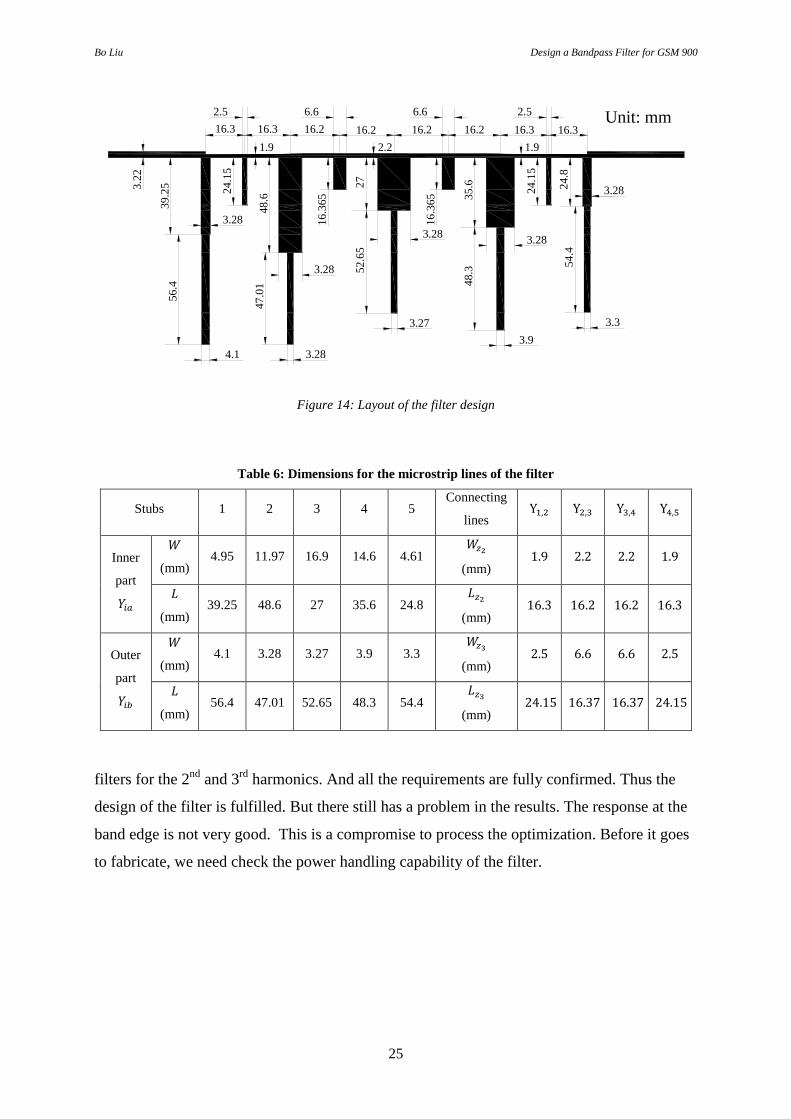
Apply the dimensions of equivalent T-shaped transmission line given above in the ADS and
process optimization, the performance of the filter after harmonic suppression is got. After
optimization, the layout of the design is shown in Fig. 14. And the dimensions of the each
microstrip line are list in Table. 5.
Fig. 15 shows the simulation results of the filter obtained by EM simulation after processing
the harmonics suppression and optimization. Obviously, the 2nd
and 3rd
harmonics are
suppressed, which means that the equivalent T-shaped connecting lines work as bandstop
Bo Liu Design a Bandpass Filter for GSM 900
25
39
.25
56
.4
4.1 3.28
3.27
3.9
3.3
47
.01
48
.6
24
.15
16
.36
5
27
35
.64
8.3
24
.85
4.4
52
.65
16
.36
5
24
.15
3.28
3.28
3.283.28
3.28
16.3 16.3 16.2 16.2 16.2 16.2 16.3 16.33
.22
2.5 6.6 6.6 2.5 Unit: mm
1.9 2.2 1.9
Figure 14: Layout of the filter design
Table 6: Dimensions for the microstrip lines of the filter
Stubs 1 2 3 4 5 Connecting
lines
Inner
part
(mm) 4.95 11.97 16.9 14.6 4.61
(mm)
(mm) 39.25 48.6 27 35.6 24.8
(mm)
Outer
part
(mm) 4.1 3.28 3.27 3.9 3.3
(mm)
(mm) 56.4 47.01 52.65 48.3 54.4
(mm)
filters for the 2nd
and 3rd
harmonics. And all the requirements are fully confirmed. Thus the
design of the filter is fulfilled. But there still has a problem in the results. The response at the
band edge is not very good. This is a compromise to process the optimization. Before it goes
to fabricate, we need check the power handling capability of the filter.

Bo Liu Design a Bandpass Filter for GSM 900
26
(a)
(b)
Figure 15: Frequency response (a) and phase response (b) after processing harmonics suppression
3.7 Manufacture and Results
Since the operation powers of this bandpass filter are 200 W RMS and 800 W peak power, we
need check the power handling capability of the filter before it goes to fabricate. If the design
can survive under such high power, we will bring about the design into fabrication. Protomat
E33 is used to engrave the figure of the filter on a Rogers RT6035HTC PCB laminate. Finally,
measurement on VNA and discussion based on the comparison with the simulation results
will be present.
3.7.1 Calculation of Power Handling Capability of the Design
According to the theory described in Pozars Microwave Engineering, the current will never
go through the shunt open-circuited stubs since the impedance of these microstrip lines are
close to infinite [8]. Thus the power handling capability of the half-wavelength open-circuited
stubs filter is determined by the series connecting lines. Typically in this design, calculations
of the APHC only focus on the series connecting transmission lines of the equivalent T-
shaped structure. Using the method described in theory part associated with the data of the

Bo Liu Design a Bandpass Filter for GSM 900
27
PCB laminate, we can compute the theoretical value of how much power the design can
handle.
The RT6035 PCB laminate is a kind of multilayer laminate. The structure of it is briefly
shown in Fig. 14. For the calculation of APHC of the multilayer laminate, we need to know
the thickness of the PTFE layer d and the ceramic layer h. But there have no data of them
from Rogers Corp. therefore, for the convenient of the calculation, we assume the thickness
of PTFE supporting dielectric layers is equal to zero, that is d+h equal to h, since the
thickness of the PTFE layer is negligible compared to the height of ceramic layer. Applying
the Eq. (50) to (56) described in theory part associated with the dimensions of the equivalent
T-shaped transmission line and the datasheet of the RT6035 PCB laminate list in Table. 2, the
maximum range for power handling of the design can be calculated. The computed results are
summarized in Table. 7.
Table 7: Calculation results of APHC of the filter
Series connecting lines
Impedance 66.87 62 62 66.87
0.9566 1.0904 1.0904 0.9566
2.6532 2.6752 2.6752 2.6532
Equivalent width of the strip (mm) 0.0086 0.0093 0.0093 0.0086
0.0873 0.0942 0.0942 0.0873
0.1835 0.1835 0.1835 0.1835
Power handling (W) 989.7 1190.4 1190.4 989.7
It’s clearly to find out from Table. 7, the APHC for each series connecting lines is larger than
the required peak power. Thus this design can operate properly under such high power. In
other words, the requirement on power handling capability of the design is fulfilled.
3.7.2 Manufacture and Measurement Results
The designed filter will be fabricated on a RT6035 PCB laminate with the dimensions of 228
×150 mm by using LPKF Protomat E33. The size of layout with feeding lines of the design
is 130×122 mm. Applying the ADS layout with feeding lines of the design in the control
program of LPKF Protomat E33, the figure of the filter is milled out shown in Fig. 16. Instead

Bo Liu Design a Bandpass Filter for GSM 900
28
of polishing all copper surfaces, we just engrave the curve of the filter out and set a interval
with distance of 0.2 mm to separate filter from the ground plate. The interval will isolate the
microstrip transmission lines and the surface conductor.
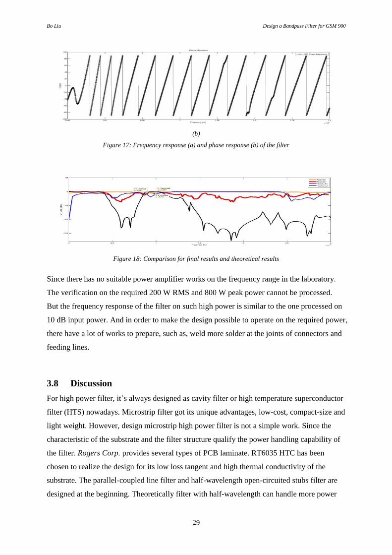
Fig.17 shows the frequency and phase response of the filter after processing basic
measurement on VNA with input power of 10 dB. Obviously, the phase information in the
passband of the filter is linear. This is necessary since the filter with linear phase has constant
group delay and transmit signal without distortion. But it can also see that the frequency
response of the filter is not satisfied with the theoretical results. There has an additional
passband in the vicinity of . Although S21 (around -1.3dBm) and S11 (around -15dBm)
are close to the requirement in the fundamental passband, there has a spike appear at 800
MHz. The suppression of harmonics is realized, but it also needs to improve. At the 2nd
harmonic, the frequency response is achieved the requirement. However, at the 3rd
harmonic,
S21 (around -10dBm) is also too large. And comparison of the measurement and simulation
results is shown in Fig.18.
Figure 16: Designed filter with connectors
(a)
Bo Liu Design a Bandpass Filter for GSM 900
29
(b)
Figure 17: Frequency response (a) and phase response (b) of the filter
Figure 18: Comparison for final results and theoretical results
Since there has no suitable power amplifier works on the frequency range in the laboratory.
The verification on the required 200 W RMS and 800 W peak power cannot be processed.
But the frequency response of the filter on such high power is similar to the one processed on
10 dB input power. And in order to make the design possible to operate on the required power,
there have a lot of works to prepare, such as, weld more solder at the joints of connectors and
feeding lines.
3.8 Discussion
For high power filter, it’s always designed as cavity filter or high temperature superconductor
filter (HTS) nowadays. Microstrip filter got its unique advantages, low-cost, compact-size and
light weight. However, design microstrip high power filter is not a simple work. Since the
characteristic of the substrate and the filter structure qualify the power handling capability of
the filter. Rogers Corp. provides several types of PCB laminate. RT6035 HTC has been
chosen to realize the design for its low loss tangent and high thermal conductivity of the
substrate. The parallel-coupled line filter and half-wavelength open-circuited stubs filter are
designed at the beginning. Theoretically filter with half-wavelength can handle more power

Bo Liu Design a Bandpass Filter for GSM 900
30
than parallel-coupled line filter. In order to simplify the calculation and structure, 5th
order
half-wavelength open-circuited stubs filter has been chosen for the symmetry of the structure.
The 2nd
and 3rd
harmonics of the structure have been suppressed by using equivalent T-shaped
transmission line method. And this type of filter have additional passbands in the vicinity of
and , and at other corresponding periodic frequencies.
Measurements of the filter (Fig. 18) show some differences between the simulation results
(Fig.13a). There is a spike appearing in the left of the passband and the suppression of the 3rd
harmonic is inappropriate. There are some reasons leading to the phenomenal. When simulate
microstrip line on ADS, the result is not really accurate for very wide stubs. For this design,
the width of the microstrip line varies from 1.9mm to 16.9mm, which may impact the
performance of the filter. The effect of step-in-width is also need to be considered since we
choose different admittance in the inner and outer part of open-circuited stubs when design
the filter. Besides, due to the restriction of conditions, we do not polish all the ground copper
when using LPKT Protomat E33. This may not provide enough isolation between the
transmission lines and the ground plate. Thus there will have coupling between them.
The calculation results show that the filter can easily handle the average 200W. However the
measurement on such power cannot be processed since there is no suitable power amplifier in
the laboratory.

Bo Liu Design a Bandpass Filter for GSM 900
31
4 CONCLUSION
In this thesis work, the method to implement the high power bandpass filter has been
presented. The filter which is working on the average power of 200W compacted with 2nd
and
3rd
harmonic suppression has been demonstrated on the substrate of RT6035HTC. The design
is fulfilled by using half-wavelength open-circuit stubs compacted with equivalent T-shaped
connecting lines. The structure of the stubs filter provides enough power handling capability
of the filter. Besides, the equivalent T-shaped connecting transmission line act as bandstop
filters for the harmonics without changing the response of the fundamental frequency. Thus
the purpose of the design is fulfilled. The concept of compact structure is validated though
simulation and implementation. Measurement results of the fabricated filter shows that the
filter works properly under such high power, the 2nd
and 3rd
harmonic are also satisfy the
requirement.

Bo Liu Design a Bandpass Filter for GSM 900
32
REFERENCES
[1] J. S Hong and M. J. Lancaster, Microstrip Filters for RF/Microwave Applications. New
York: Wiley, pp. 153–158, Jul. 2001.
[2] I. J. Bahl and K. C. Gupta, “Avarage power-handling capability of microstrip lines,”
IEE Proc.—H., Microwave, Optics, Acoustics, vol. 3, pp. 1–4, Jan. 1979.
[3] Y. G. Choi, and B. K. Kim, “Design of a 5.8 GHz Broadband BPFs with Second
Harmonics Suppression Using Open-Stubs,” APMC Proc., 2007, pp. 2281-2284.
[4] I. J. Bahl and D. K. Trivedi publish their paper "A Designer's Guide to Microstrip
Line," Microwaves, pp. 174, May 1977.
[5] I. J. Bahl, Lumped Elements for RF and Microwave Circuits. Norwood, MA: Artech, pp.
447-452, Apr. 2003.
[6] R. J. Cameron, C. M.Kudsia, and R. R. Mansour, Microwave Filters for Communication
Systems-Fundamentals, Design, and Applications. New York: Wiley, Jul. 2007.
[7] J. S Hong and M. J. Lancaster, Microstrip Filters for RF/Microwave Applications. New
York: Wiley, pp. 89-91, Jul. 2001.
[8] D. M. Pozar, Microwave Engineering, 4th Ed. New York: Wiley, pp.256-258, Mar.
2011.
[9] J. S Hong and M. J. Lancaster, Microstrip Filters for RF/Microwave Applications. New
York: Wiley, pp. 89-91, Jul. 2001.
[10] E. J. Denlinger, “Losses of microstrip lines,” IEEE Trans., MTT-28, pp. 513–522, Jun.
1980.
[11] R. A. Pucel, D. J. Masse, and C. P. Hartwig, “Losses in microstrip,” IEEE Trans., MTT-
16, June 1968, 342–350. Correction in IEEE Trans., MTT-16, p. 1064, Dec. 1968.
[12] J. R. Lee, J. H. Cho, and S. W. Yun, "New compact bandpass filter using microstrip X/4
resonators with open stub inverter," IEEE Microwave Guided-wave Lett., vol. 10, no.12,
pp. 526-527, Dec. 2002.
[13] I. J. Bahl, ‘‘Average Power Handling Capability of Multilayer Microstrip Lines,’’ Int. J.
RF and Microwave Computer-Aided Engineering, Vol. 11, pp. 385–395, Nov. 2001.
[14] M. Kirschning, R. H. Jansen, and N. H. L. Koster, “Accurate model for open end effect
of microstrip lines,” Electronics Letters, 17, pp. 123–125, Feb. 1981.
[15] A. Machec, C. Quendo, E. Rius, C. Person, and J. F. Favenec, "Synthesis of dual
behavior resonator (DBR) filters with integrated low pass structures for spurious
Bo Liu Design a Bandpass Filter for GSM 900
33
responses suppression," IEEE Microwave Wireless Components Lett., vol. 16, no. 1, pp.
1531-1309, Jan. 2006.
[16] I. J. Bahl, Lumped Elements for RF and Microwave Circuits. Norwood, MA: Artech, pp.
444-446, Apr. 2003.
[17] W. H. Tu and K. Chang, “Compact second harmonic-suppressed bandstop and bandpass
filters using open stubs,” IEEE Trans. Microw. Theory Tech., vol. 54, no. 6, pp. 2497–
2502, Jun. 2006.

Bo Liu Design a Bandpass Filter for GSM 900
34
APPENDIX - MATLAB SCRIPT OF THE DESIGN EQUATION
% for 5th order %
g0=1;
g1=1.1468;
g2=1.3712;
g3=1.975;
g4=1.3712;
g5=1.1468;
g6=1;
% filter design %
O=0.47375*pi;
h=2
A1=(h*g1/g2)^(0.5);
A2=(h*g1)/((g2*g3)^(0.5));
A3=((h*g1*g5)/(g0*g3))^(0.5);
h*g1*tan(O)/2
N1=(A1^2+(h*g1*tan(O)/2)^2)^(0.5);
N2=(A2^2+(h*g1*tan(O)/2)^2)^(0.5);
N3=(A3^2+(h*g1*tan(O)/2)^2)^(0.5);
S=tan(O);
Y0=1/50;
Y1=g0*Y0*(1-h/2)*g1*tan(O)+Y0*(N1-A1);
Y2=Y0*(N1+N2-A1-A2);
Y3=Y0*(N2+N3-A2-A3);
Y4=Y0*((g4*g5-g0*g1*h/2)*tan(O)+(N3-A3));
f0=0.9487;
a1=1;
Y1a=Y1*(a1*((tan(O))^2)-1)/((a1+1)*((tan(O))^2));
a2=1;
Y2a=Y2*(a2*((tan(O))^2)-1)/((a2+1)*((tan(O))^2));
a3=1;
Y3a=Y3*(a3*((tan(O))^2)-1)/((a3+1)*((tan(O))^2));
a4=1;
Y4a=Y4*(a4*((tan(O))^2)-1)/((a4+1)*((tan(O))^2));
Y1b=a1*Y1a;
Y2b=a2*Y2a;
Y3b=a3*Y3a;
Y4b=a4*Y4a;

Bo Liu Design a Bandpass Filter for GSM 900
35
Y12=Y0*(A1);
Y23=Y0*(A2);
% Calculate the Ere %
W=0.385;
h=0.635;
Er=10.2;
f=10;
if W/h<=1
Ere=(Er+1)/2+((Er-1)/2)*((1+12*h/W)^(-0.5)+0.04*(1-W/h));
Zc=120*pi*log(8*h/W+0.25*W/h)/(2*pi*((Er)^(0.5)));
else
Ere=(Er+1)/2+((Er-1)/2)*((1+12*h/W)^(-0.5));
Zc=120*pi*((W/h+1.393+0.677*log(W/h+1.444))^-1)/((Er)^(0.5));
end
Wavel=300/(f*((Er)^(0.5)));
Z0=51.86;
b=377*pi/2/Z0/(3.6^0.5);
Wd=2/pi*(b-1-log(2*b-1)+1.3/3.6*(log(b-1)+0.39-0.61/3.6));
dW=1/Wd;
Er=2.3+1.3/((1+12*dW)^0.5)
Z0=50.948;
b=377*pi/2/Z0/(3.6^0.5);
Wd=2/pi*(b-1-log(2*b-1)+1.3/3.6*(log(b-1)+0.39-0.61/3.6));
dW=1/Wd;
Er=2.3+1.3/((1+12*dW)^0.5)
Z0=52.846;
b=377*pi/2/Z0/(3.6^0.5);
Wd=2/pi*(b-1-log(2*b-1)+1.3/3.6*(log(b-1)+0.39-0.61/3.6));
dW=1/Wd;
Er=2.3+1.3/((1+12*dW)^0.5)
% Compensation for the Microstrip Open End %
Ere=2.8819;
Wd=3.0061;
d=1.4471;
E1=0.434907*(Ere^0.81+0.26*(Wd^0.8544)+0.236)/(Ere^0.81-
0.189*(Wd^0.8544)+0.87);
E2=1+(Wd^0.371)/(2.35*3.6+1);
E3=1+(0.5274*atan(0.084*(Wd^(1.9413/E2))))/(Ere^0.9236);
E4=1+0.037*atan(0.067*(Wd^1.456))*(6-5*exp(0.036*(1-3.6)));
Bo Liu Design a Bandpass Filter for GSM 900
36
E5=1-0.218*exp(-7.5*Wd);
l=E1*E3*E5/E4*d
% Average Power Handling Capacitance calculation %
cond=5.813*10^7;
u0=4*pi*10^(-7);
W=0.0019;
Er=3.6;
Ere=2.6532;
Losst=0.0013;
Kg=30;
f0=0.948*10^9;
h=0.001524;
Z0=62;
wavel=3*10^8/(f0*(3.6)^0.5)
We=120*pi*(0.001524)/Z0;
ac=8.686*((f0/(2*pi)*u0/(2*cond))^(0.5))/(Z0*W);
ad=8.686*pi*(Ere-1)/(Er-1)*Er/Ere*Losst/wavel;
APHC=(150-23)/(0.2303*(ac*(h/(We*Kg))+ad*(h/(2*We*Kg))));