Description Quick Setup Guide - Intersil · ISL85415DEMO1Z Wide VIN 500mA Synchronous Buck...
12
USER’S MANUAL AN1860 Rev 2.00 May 16, 2014 ISL85415DEMO1Z Wide VIN 500mA Synchronous Buck Regulator AN1860 Rev 2.00 Page 1 of 12 May 16, 2014 Description The ISL85415DEMO1Z kit is intended for use for point-of-load applications sourcing from 3V to 36V. The kit is used to demonstrate the performance of the ISL85415 Wide V IN Low Quiescent Current High Efficiency Sync Buck Regulator with 500mA output current. The ISL85415 is offered in a 4mmx3mm 12 Ld DFN package with 1mm maximum height. The converter occupies 1.516 cm 2 area. Key Features • Wide input voltage range 3V to 36V • Synchronous operation for high efficiency • No compensation required • Integrated high-side and low-side NMOS devices • Selectable PFM or forced PWM mode at light loads • Internal fixed (500kHz) or adjustable switching frequency 300kHz to 2MHz • Continuous output current up to 500mA • Internal or external soft-start • Minimal external components required • Power-good and enable functions available Recommended Equipment The following materials are recommended to perform testing: • 0V to 50V power supply with at least 2A source current capability • Electronic Loads capable of sinking current up to 1.5A • Digital multimeters (DMMs) • 100MHz quad-trace oscilloscope • Signal generator Quick Setup Guide 1. Ensure that the circuit is correctly connected to the supply and loads prior to applying any power. 2. Connect the bias supply to VIN, the plus terminal to VIN (P4) and the negative return to GND (P5). 3. Turn on the power supply. 4. Verify the output voltage is 3.3V for V OUT. Evaluating the Other Output Voltage The ISL85415DEMO1Z kit output is preset to 3.3V; however, output voltages can be adjusted from 0.6V to 15V. The output voltage programming resistor, R 2 , will depend on the desired output voltage of the regulator and the value of the feedback resistor R 1 , as shown in Equation 1 . If the output voltage desired is 0.6V, then R 1 is shorted. Please note that if V OUT is less than 1.8V, the switching frequency and compensation must be changed for 300kHz operation due to minimum on-time limitation. Please refer to datasheet ISL85415 for further information. Table 1 on page 2 shows the component selection that should be used for the respective V OUTs . R 2 R 1 0.6 V OUT 0.6 – --------------------------- = (EQ. 1) FIGURE 1. FRONT OF EVALUATION BOARD ISL85415DEMO1Z FIGURE 2. BACK OF EVALUATION BOARD ISL85415DEMO1Z
Transcript of Description Quick Setup Guide - Intersil · ISL85415DEMO1Z Wide VIN 500mA Synchronous Buck...

USER’S MANUAL
AN1860Rev 2.00
May 16, 2014
ISL85415DEMO1ZWide VIN 500mA Synchronous Buck Regulator
DescriptionThe ISL85415DEMO1Z kit is intended for use for point-of-load applications sourcing from 3V to 36V. The kit is used to demonstrate the performance of the ISL85415 Wide VIN Low Quiescent Current High Efficiency Sync Buck Regulator with 500mA output current.
The ISL85415 is offered in a 4mmx3mm 12 Ld DFN package with 1mm maximum height. The converter occupies 1.516 cm2 area.
Key Features• Wide input voltage range 3V to 36V
• Synchronous operation for high efficiency
• No compensation required
• Integrated high-side and low-side NMOS devices
• Selectable PFM or forced PWM mode at light loads
• Internal fixed (500kHz) or adjustable switching frequency 300kHz to 2MHz
• Continuous output current up to 500mA
• Internal or external soft-start
• Minimal external components required
• Power-good and enable functions available
Recommended EquipmentThe following materials are recommended to perform testing:
• 0V to 50V power supply with at least 2A source current capability
• Electronic Loads capable of sinking current up to 1.5A
• Digital multimeters (DMMs)
• 100MHz quad-trace oscilloscope
• Signal generator
Quick Setup Guide 1. Ensure that the circuit is correctly connected to the supply
and loads prior to applying any power.
2. Connect the bias supply to VIN, the plus terminal to VIN (P4) and the negative return to GND (P5).
3. Turn on the power supply.
4. Verify the output voltage is 3.3V for VOUT.
Evaluating the Other Output VoltageThe ISL85415DEMO1Z kit output is preset to 3.3V; however, output voltages can be adjusted from 0.6V to 15V. The output voltage programming resistor, R2, will depend on the desired output voltage of the regulator and the value of the feedback resistor R1, as shown in Equation 1.
If the output voltage desired is 0.6V, then R1 is shorted. Please note that if VOUT is less than 1.8V, the switching frequency and compensation must be changed for 300kHz operation due to minimum on-time limitation. Please refer to datasheet ISL85415 for further information.
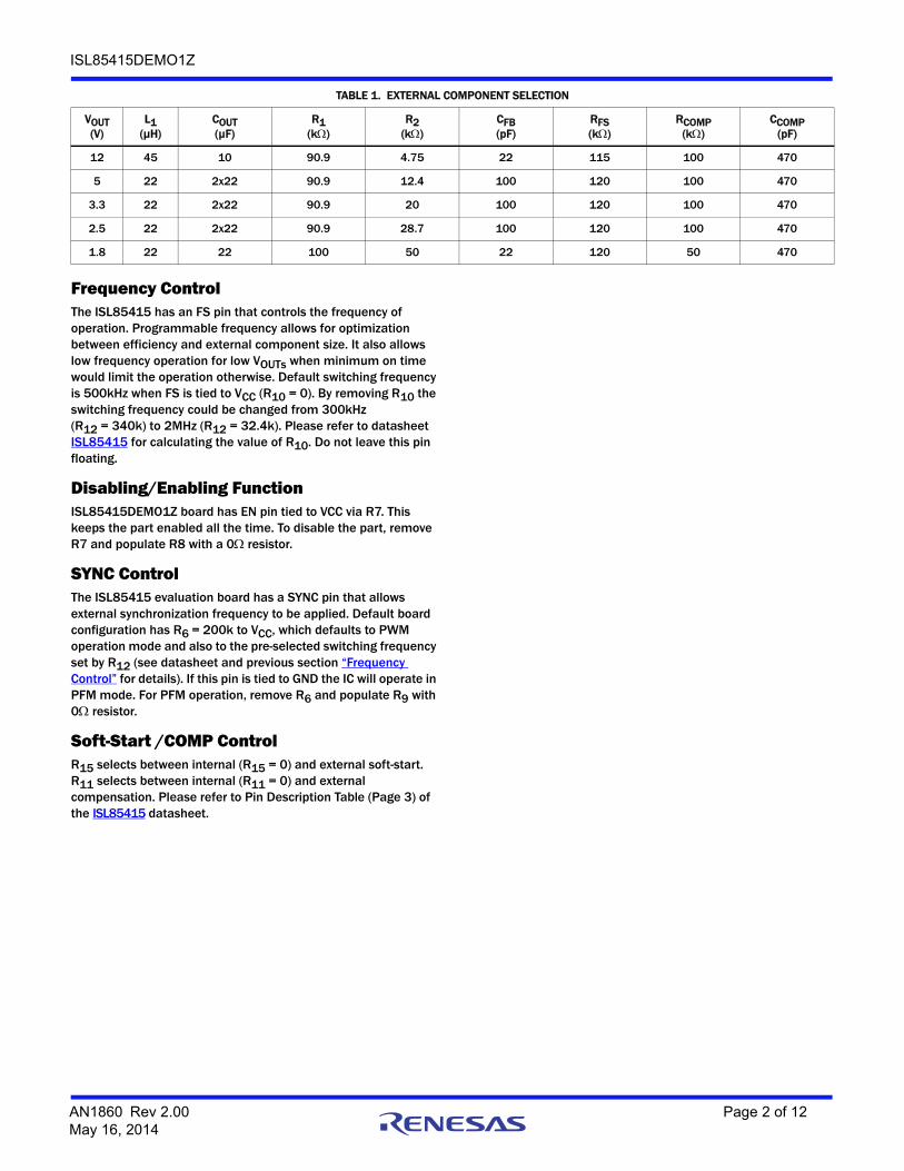
Table 1 on page 2 shows the component selection that should be used for the respective VOUTs.
R2 R10.6
VOUT 0.6–--------------------------- = (EQ. 1)
FIGURE 1. FRONT OF EVALUATION BOARD ISL85415DEMO1Z FIGURE 2. BACK OF EVALUATION BOARD ISL85415DEMO1Z
AN1860 Rev 2.00 Page 1 of 12May 16, 2014
ISL85415DEMO1Z
Frequency ControlThe ISL85415 has an FS pin that controls the frequency of operation. Programmable frequency allows for optimization between efficiency and external component size. It also allows low frequency operation for low VOUTs when minimum on time would limit the operation otherwise. Default switching frequency is 500kHz when FS is tied to VCC (R10 = 0). By removing R10 the switching frequency could be changed from 300kHz (R12 = 340k) to 2MHz (R12 = 32.4k). Please refer to datasheet ISL85415 for calculating the value of R10. Do not leave this pin floating.
Disabling/Enabling FunctionISL85415DEMO1Z board has EN pin tied to VCC via R7. This keeps the part enabled all the time. To disable the part, remove R7 and populate R8 with a 0 resistor.
SYNC ControlThe ISL85415 evaluation board has a SYNC pin that allows external synchronization frequency to be applied. Default board configuration has R6 = 200k to VCC, which defaults to PWM operation mode and also to the pre-selected switching frequency set by R12 (see datasheet and previous section “Frequency Control” for details). If this pin is tied to GND the IC will operate in PFM mode. For PFM operation, remove R6 and populate R9 with 0 resistor.
Soft-Start /COMP ControlR15 selects between internal (R15 = 0) and external soft-start. R11 selects between internal (R11 = 0) and external compensation. Please refer to Pin Description Table (Page 3) of the ISL85415 datasheet.
TABLE 1. EXTERNAL COMPONENT SELECTION
VOUT(V)
L1(µH)
COUT(µF)
R1(k)
R2(k)
CFB(pF)
RFS(k)
RCOMP(k)
CCOMP(pF)
12 45 10 90.9 4.75 22 115 100 470
5 22 2x22 90.9 12.4 100 120 100 470
3.3 22 2x22 90.9 20 100 120 100 470
2.5 22 2x22 90.9 28.7 100 120 100 470
1.8 22 22 100 50 22 120 50 470
AN1860 Rev 2.00 Page 2 of 12May 16, 2014
ISL85415DEMO1Z
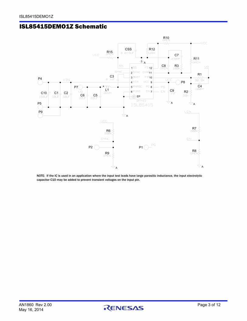
ISL85415DEMO1Z Schematic
PHASE
PGND
0.1UFVIN
BOOT
SYNC
SS
PG
FS
COMP
VCC
FB
EN
ISL85415
VCC
150UF 10UF
ENPG
VCC
1UF
22UF
VO
100K
120K
VIN
DFN1210UF
OPEN
22UF
200K
SYNC
PG
OPEN
VIN
VCC
22UH
EN
200K
100PF
OPEN470PF
0.033UFVCC
20K
90.9K
VO
OPEN
OPEN
SS
OPEN
SYNC
?
A
8
12
11
10
9
7
5
1
2
6
4
3
EP
A
A
A
A
A
C10
C3
P9
CSS R12
C9C6
P7
R3
P8
C1C5
C8
P1R8
R7
P5
P2
R6
L1C4
R1P4
R2
R11C7
R10
C2
R9
R15
NOTE: If the IC is used in an application where the input test leads have large parasitic inductance, the input electrolytic capacitor C10 may be added to prevent transient voltages on the input pin.
AN1860 Rev 2.00 Page 3 of 12May 16, 2014
ISL85415DEMO1Z
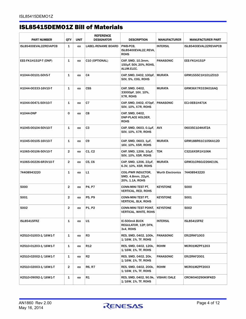
ISL85415DEMO1Z Bill of Materials
PART NUMBER QTY UNITREFERENCE DESIGNATOR DESCRIPTION MANUFACTURER MANUFACTURER PART
ISL85400EVAL2ZREVAPCB 1 ea LABEL-RENAME BOARD PWB-PCB, ISL85400EVAL2Z, REVA, ROHS
INTERSIL ISL85400EVAL2ZREVAPCB
EEE-FK1H151P-T (DNP) 1 ea C10 (OPTIONAL) CAP, SMD, 10.3mm, 150µF, 50V, 20%, ROHS, ALUM.ELEC.
PANASONIC EEE-FK1H151P
H1044-00101-50V5-T 1 ea C4 CAP, SMD, 0402, 100pF, 50V, 5%, C0G, ROHS
MURATA GRM1555C1H101JZ01D
H1044-00333-16V10-T 1 ea CSS CAP, SMD, 0402, 33000pF, 16V, 10%, X7R, ROHS
MURATA GRM36X7R333K016AQ
H1044-00471-50V10-T 1 ea C7 CAP, SMD, 0402, 470pF, 50V, 10%, X7R, ROHS
PANASONIC ECJ-0EB1H471K
H1044-DNP 0 ea C8 CAP, SMD, 0402, DNP-PLACE HOLDER, ROHS
H1045-00104-50V10-T 1 ea C3 CAP, SMD, 0603, 0.1µF, 50V, 10%, X7R, ROHS
AVX 06035C104KAT2A
H1045-00105-16V10-T 1 ea C9 CAP, SMD, 0603, 1µF, 16V, 10%, X5R, ROHS
MURATA GRM188R61C105KA12D
H1065-00106-50V10-T 2 ea C1, C2 CAP, SMD, 1206, 10µF, 50V, 10%, X5R, ROHS
TDK C3216X5R1H106K
H1065-00226-6R3V10-T 2 ea C5, C6 CAP, SMD, 1206, 22µF, 6.3V, 10%, X5R, ROHS
MURATA GRM31CR60J226KE19L
74408943220 1 ea L1 COIL-PWR INDUCTOR, SMD, 4.8mm, 22µH, 20%, 1.1A, ROHS
Wurth Electronics 74408943220
5000 2 ea P4, P7 CONN-MINI TEST PT, VERTICAL, RED, ROHS
KEYSTONE 5000
5001 2 ea P5, P9 CONN-MINI TEST PT, VERTICAL, BLK, ROHS
KEYSTONE 5001
5002 2 ea P1, P2 CONN-MINI TEST POINT, VERTICAL, WHITE, ROHS
KEYSTONE 5002
ISL85415FRZ 1 ea U1 IC-500mA BUCK REGULATOR, 12P, DFN, 3x4, ROHS
INTERSIL ISL85415FRZ
H2510-01003-1/16W1-T 1 ea R3 RES, SMD, 0402, 100k, 1/16W, 1%, TF, ROHS
PANASONIC ERJ2RKF1003
H2510-01203-1/16W1-T 1 ea R12 RES, SMD, 0402, 120k, 1/16W, 1%, TF, ROHS
ROHM MCR01MZPF1203
H2510-02002-1/16W1-T 1 ea R2 RES, SMD, 0402, 20k, 1/16W, 1%, TF, ROHS
PANASONIC ERJ2RKF2001
H2510-02003-1/16W1-T 2 ea R6, R7 RES, SMD, 0402, 200k, 1/16W, 1%, TF, ROHS
ROHM MCR01MZPF2003
H2510-09092-1/16W1-T 1 ea R1 RES, SMD, 0402, 90.9k, 1/16W, 1%, TF, ROHS
VISHAY/DALE CRCW040290K9FKED
AN1860 Rev 2.00 Page 4 of 12May 16, 2014

ISL85415DEMO1Z
H2510-DNP 0 ea R8-R11, R15 RES, SMD, 0402, DNP, DNP, DNP, TF, ROHS
2X3-STATIC-BAG 1 ea PLACE ASSY IN BAG BAG, STATIC, 2x3, ZIP LOC
TBD S-6509
LABEL-DATE CODE 1 ea AFFIX TO BACK OF PCB LABEL-DATE CODE_BOM REV#_SERIAL# LABEL ON ZIL & QUEL
INTERSIL LABEL-DATE CODE
LABEL-RENAME BOARD 1 ea RENAME TOP PCB TO: ISL85415DEMO1Z
LABEL, TO RENAME BOARD
INTERSIL LABEL-RENAME BOARD
ISL85415DEMO1Z Bill of Materials (Continued)
PART NUMBER QTY UNITREFERENCE DESIGNATOR DESCRIPTION MANUFACTURER MANUFACTURER PART
ISL85415DEMO1Z Board Layout
FIGURE 3. SILK SCREEN TOP
AN1860 Rev 2.00 Page 5 of 12May 16, 2014

ISL85415DEMO1Z
FIGURE 4. SILKSCREEN BOTTOM
ISL85415DEMO1Z Board Layout (Continued)
Efficiency Curves FSW = 800kHz, TA = +25°C
FIGURE 5. EFFICIENCY vs LOAD, PFM, VOUT = 5V FIGURE 6. EFFICIENCY vs LOAD, PWM, VOUT = 5V
50
55
60
65
70
75
80
85
90
95
100
0 0.05 0.10 0.15 0.20 0.25 0.30 0.35 0.40 0.45 0.50
VVVVV
OUTPUT LOAD (A)
EF
FIC
IEN
CY
(%
)
VIN = 15V
VIN = 24V VIN = 33V
VIN = 12V VIN = 6V
50
55
60
65
70
75
80
85
90
95
100
0 0.05 0.10 0.15 0.20 0.25 0.30 0.35 0.40 0.45 0.50
OUTPUT LOAD (A)
EF
FIC
IEN
CY
(%
)
VIN = 6V
VIN = 15V
VIN = 24V
VIN = 33V
VIN = 12V
AN1860 Rev 2.00 Page 6 of 12May 16, 2014

ISL85415DEMO1Z
FIGURE 7. EFFICIENCY vs LOAD, PFM, VOUT = 3.3V FIGURE 8. EFFICIENCY vs LOAD, PWM, VOUT = 3.3V
FIGURE 9. EFFICIENCY vs LOAD, PFM, VOUT = 1.8V FIGURE 10. EFFICIENCY vs LOAD, PWM, VOUT = 1.8V
FIGURE 11. VOUT REGULATION vs LOAD, PWM, VOUT = 5V FIGURE 12. VOUT REGULATION vs LOAD, PFM, VOUT = 5V
Efficiency Curves FSW = 800kHz, TA = +25°C (Continued)
50
55
60
65
70
75
80
85
90
95
100
0 0.05 0.10 0.15 0.20 0.25 0.30 0.35 0.40 0.45 0.50
OUTPUT LOAD (A)
EF
FIC
IEN
CY
(%
)
VIN = 5V VIN = 15V
VIN = 24V VIN = 33V
VIN = 12V
50
55
60
65
70
75
80
85
90
95
100
0 0.05 0.10 0.15 0.20 0.25 0.30 0.35 0.40 0.45 0.50
OUTPUT LOAD (A)
EF
FIC
IEN
CY
(%
)
VIN = 5V VIN = 15V
VIN = 24V VIN = 33V
VIN = 12V
50
55
60
65
70
75
80
85
90
95
100
0 0.05 0.10 0.15 0.20 0.25 0.30 0.35 0.40 0.45 0.50
OUTPUT LOAD (A)
EF
FIC
IEN
CY
(%
)
VIN = 5V VIN = 15V
VIN = 24V VIN = 33V
VIN = 12V
50
55
60
65
70
75
80
85
90
95
100
0 0.05 0.10 0.15 0.20 0.25 0.30 0.35 0.40 0.45 0.50
OUTPUT LOAD (A)
EF
FIC
IEN
CY
(%
)VIN = 5V VIN = 15V
VIN = 24V VIN = 33V
VIN = 12V
5.004
5.006
5.008
5.010
5.012
5.014
5.016
5.018
0 0.05 0.10 0.15 0.20 0.25 0.30 0.35 0.40 0.45 0.50
OUTPUT LOAD (A)
OU
TP
UT
VO
LT
AG
E (
V)
VIN = 6V
VIN = 15V
VIN = 24V
VIN = 33V
VIN = 12V
4.975
4.980
4.985
4.990
4.995
5.000
5.005
5.010
5.015
5.020
0 0.05 0.10 0.15 0.20 0.25 0.30 0.35 0.40 0.45 0.50
VIN = 6V
VIN = 15V
VIN = 24V
VIN = 33V
VIN = 12V
OUTPUT LOAD (A)
OU
TP
UT
VO
LT
AG
E (
V)
AN1860 Rev 2.00 Page 7 of 12May 16, 2014
ISL85415DEMO1Z
FIGURE 13. VOUT REGULATION vs LOAD, PWM, VOUT = 3.3V FIGURE 14. VOUT REGULATION vs LOAD, PFM, VOUT = 3.3V
FIGURE 15. VOUT REGULATION vs LOAD, PWM, VOUT = 1.8V FIGURE 16. VOUT REGULATION vs LOAD, PFM, VOUT = 1.8V
Efficiency Curves FSW = 800kHz, TA = +25°C (Continued)
3.322
3.324
3.326
3.328
3.330
3.332
3.334
3.336
0 0.05 0.10 0.15 0.20 0.25 0.30 0.35 0.40 0.45 0.50
OUTPUT LOAD (A)
OU
TP
UT
VO
LT
AG
E (
V)
VIN = 5V
VIN = 15V
VIN = 24V
VIN = 33V
VIN = 12V
3.310
3.315
3.320
3.325
3.330
3.335
3.340
3.345
0 0.05 0.10 0.15 0.20 0.25 0.30 0.35 0.40 0.45 0.50
OUTPUT LOAD (A)
OU
TP
UT
VO
LT
AG
E (
V)
VIN = 5V VIN = 12V
VIN = 15V VIN = 24V
VIN = 33V
1.769
1.770
1.771
1.772
1.773
1.774
1.775
1.776
1.777
0 0.05 0.10 0.15 0.20 0.25 0.30 0.35 0.40 0.45 0.50
OUTPUT LOAD (A)
OU
TP
UT
VO
LT
AG
E (
V)
VIN = 5V
VIN = 15V
VIN = 24V VIN = 33V
VIN = 12V
1.755
1.760
1.765
1.770
1.775
1.780
1.785
0 0.05 0.10 0.15 0.20 0.25 0.30 0.35 0.40 0.45 0.50
OUTPUT LOAD (A)
OU
TP
UT
VO
LT
AG
E (
V) VIN = 15V
VIN = 24V VIN = 33V
VIN = 12V
VIN = 5V
Typical Performance Curves VIN = 24V, VOUT = 3.3V, FSW = 800kHz, TA = +25°C.
FIGURE 17. START-UP AT NO LOAD, PFM FIGURE 18. START-UP AT 500mA, PWM
LX 20V/DIV
VOUT 2V/DIV
EN 20V/DIV
PG 2V/DIV
5ms/DIV
LX 20V/DIV
VOUT 2V/DIV
IL 500mA/DIV
PG 2V/DIV
5ms/DIV
AN1860 Rev 2.00 Page 8 of 12May 16, 2014
ISL85415DEMO1Z
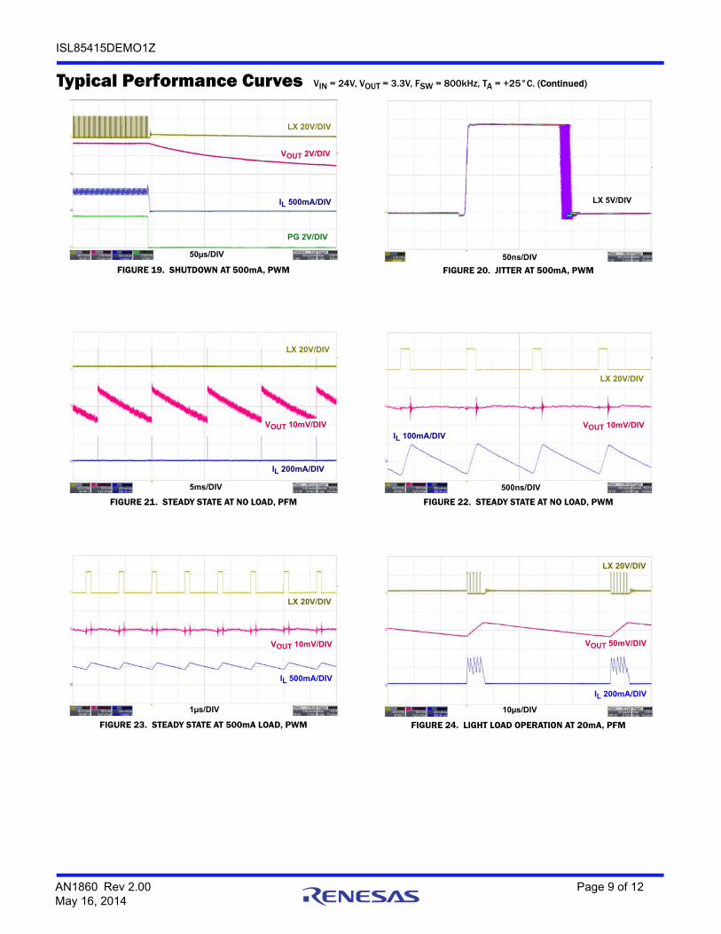
FIGURE 19. SHUTDOWN AT 500mA, PWM FIGURE 20. JITTER AT 500mA, PWM
FIGURE 21. STEADY STATE AT NO LOAD, PFM FIGURE 22. STEADY STATE AT NO LOAD, PWM
FIGURE 23. STEADY STATE AT 500mA LOAD, PWM FIGURE 24. LIGHT LOAD OPERATION AT 20mA, PFM
Typical Performance Curves VIN = 24V, VOUT = 3.3V, FSW = 800kHz, TA = +25°C. (Continued)
LX 20V/DIV
VOUT 2V/DIV
IL 500mA/DIV
PG 2V/DIV
50µs/DIV
LX 5V/DIV
50ns/DIV
LX 20V/DIV
VOUT 10mV/DIV
IL 200mA/DIV
5ms/DIV
LX 20V/DIV
VOUT 10mV/DIVIL 100mA/DIV
500ns/DIV
LX 20V/DIV
VOUT 10mV/DIV
IL 500mA/DIV
1µs/DIV 10µs/DIV
LX 20V/DIV
VOUT 50mV/DIV
IL 200mA/DIV
AN1860 Rev 2.00 Page 9 of 12May 16, 2014

ISL85415DEMO1Z
FIGURE 25. LOAD TRANSIENT, PFM FIGURE 26. LOAD TRANSIENT, PWM
FIGURE 27. PFM TO PWM TRANSITION FIGURE 28. OVERCURRENT PROTECTION, PWM
FIGURE 29. OVERCURRENT PROTECTION HICCUP, PWM FIGURE 30. SYNC AT 500mA LOAD, PWM
Typical Performance Curves VIN = 24V, VOUT = 3.3V, FSW = 800kHz, TA = +25°C. (Continued)
VOUT 100mV/DIV
IL 500mA/DIV
200µs/DIV
VOUT 50mV/DIV
IL 500mA/DIV
200µs/DIV
LX 20V/DIV
VOUT 2V/DIV
IL 1A/DIV
2µs/DIV
LX 20V/DIV
VOUT 2V/DIV
IL 500mA/DIV
PG 2V/DIV
20µs/DIV
50ms/DIV
LX 20V/DIV
VOUT 2V/DIV
IL 1A/DIV
PG 2V/DIV
LX 20V/DIV
SYNC 2V/DIV
200ns/DIV
AN1860 Rev 2.00 Page 10 of 12May 16, 2014

ISL85415DEMO1Z
FIGURE 31. NEGATIVE CURRENT LIMIT, PWM FIGURE 32. NEGATIVE CURRENT LIMIT RECOVERY, PWM
FIGURE 33. OVER-TEMPERATURE PROTECTION, PWM
Typical Performance Curves VIN = 24V, VOUT = 3.3V, FSW = 800kHz, TA = +25°C. (Continued)
LX 20V/DIV
VOUT 5V/DIV
IL 0.5A/DIV
PG 2V/DIV
10µs/DIV
LX 20V/DIV
VOUT 5V/DIV
PG 2V/DIV
200µs/DIV
IL 0.5A/DIV
VOUT 2V/DIV
PG 2V/DIV
500µs/DIV
AN1860 Rev 2.00 Page 11 of 12May 16, 2014

http://www.renesas.comRefer to "http://www.renesas.com/" for the latest and detailed information.
Renesas Electronics America Inc.1001 Murphy Ranch Road, Milpitas, CA 95035, U.S.A.Tel: +1-408-432-8888, Fax: +1-408-434-5351Renesas Electronics Canada Limited9251 Yonge Street, Suite 8309 Richmond Hill, Ontario Canada L4C 9T3Tel: +1-905-237-2004Renesas Electronics Europe LimitedDukes Meadow, Millboard Road, Bourne End, Buckinghamshire, SL8 5FH, U.KTel: +44-1628-651-700, Fax: +44-1628-651-804Renesas Electronics Europe GmbHArcadiastrasse 10, 40472 Düsseldorf, Germany Tel: +49-211-6503-0, Fax: +49-211-6503-1327Renesas Electronics (China) Co., Ltd.Room 1709 Quantum Plaza, No.27 ZhichunLu, Haidian District, Beijing, 100191 P. R. ChinaTel: +86-10-8235-1155, Fax: +86-10-8235-7679Renesas Electronics (Shanghai) Co., Ltd.Unit 301, Tower A, Central Towers, 555 Langao Road, Putuo District, Shanghai, 200333 P. R. China Tel: +86-21-2226-0888, Fax: +86-21-2226-0999Renesas Electronics Hong Kong LimitedUnit 1601-1611, 16/F., Tower 2, Grand Century Place, 193 Prince Edward Road West, Mongkok, Kowloon, Hong KongTel: +852-2265-6688, Fax: +852 2886-9022Renesas Electronics Taiwan Co., Ltd.13F, No. 363, Fu Shing North Road, Taipei 10543, TaiwanTel: +886-2-8175-9600, Fax: +886 2-8175-9670Renesas Electronics Singapore Pte. Ltd.80 Bendemeer Road, Unit #06-02 Hyflux Innovation Centre, Singapore 339949Tel: +65-6213-0200, Fax: +65-6213-0300Renesas Electronics Malaysia Sdn.Bhd.Unit 1207, Block B, Menara Amcorp, Amcorp Trade Centre, No. 18, Jln Persiaran Barat, 46050 Petaling Jaya, Selangor Darul Ehsan, MalaysiaTel: +60-3-7955-9390, Fax: +60-3-7955-9510Renesas Electronics India Pvt. Ltd.No.777C, 100 Feet Road, HAL 2nd Stage, Indiranagar, Bangalore 560 038, IndiaTel: +91-80-67208700, Fax: +91-80-67208777Renesas Electronics Korea Co., Ltd.17F, KAMCO Yangjae Tower, 262, Gangnam-daero, Gangnam-gu, Seoul, 06265 KoreaTel: +82-2-558-3737, Fax: +82-2-558-5338
SALES OFFICES
© 2018 Renesas Electronics Corporation. All rights reserved.Colophon 7.0
(Rev.4.0-1 November 2017)
Notice
1. Descriptions of circuits, software and other related information in this document are provided only to illustrate the operation of semiconductor products and application examples. You are fully responsible for
the incorporation or any other use of the circuits, software, and information in the design of your product or system. Renesas Electronics disclaims any and all liability for any losses and damages incurred by
you or third parties arising from the use of these circuits, software, or information.
2. Renesas Electronics hereby expressly disclaims any warranties against and liability for infringement or any other claims involving patents, copyrights, or other intellectual property rights of third parties, by or
arising from the use of Renesas Electronics products or technical information described in this document, including but not limited to, the product data, drawings, charts, programs, algorithms, and application
examples.
3. No license, express, implied or otherwise, is granted hereby under any patents, copyrights or other intellectual property rights of Renesas Electronics or others.
4. You shall not alter, modify, copy, or reverse engineer any Renesas Electronics product, whether in whole or in part. Renesas Electronics disclaims any and all liability for any losses or damages incurred by
you or third parties arising from such alteration, modification, copying or reverse engineering.
5. Renesas Electronics products are classified according to the following two quality grades: “Standard” and “High Quality”. The intended applications for each Renesas Electronics product depends on the
product’s quality grade, as indicated below.
"Standard": Computers; office equipment; communications equipment; test and measurement equipment; audio and visual equipment; home electronic appliances; machine tools; personal electronic
equipment; industrial robots; etc.
"High Quality": Transportation equipment (automobiles, trains, ships, etc.); traffic control (traffic lights); large-scale communication equipment; key financial terminal systems; safety control equipment; etc.
Unless expressly designated as a high reliability product or a product for harsh environments in a Renesas Electronics data sheet or other Renesas Electronics document, Renesas Electronics products are
not intended or authorized for use in products or systems that may pose a direct threat to human life or bodily injury (artificial life support devices or systems; surgical implantations; etc.), or may cause
serious property damage (space system; undersea repeaters; nuclear power control systems; aircraft control systems; key plant systems; military equipment; etc.). Renesas Electronics disclaims any and all
liability for any damages or losses incurred by you or any third parties arising from the use of any Renesas Electronics product that is inconsistent with any Renesas Electronics data sheet, user’s manual or
other Renesas Electronics document.
6. When using Renesas Electronics products, refer to the latest product information (data sheets, user’s manuals, application notes, “General Notes for Handling and Using Semiconductor Devices” in the
reliability handbook, etc.), and ensure that usage conditions are within the ranges specified by Renesas Electronics with respect to maximum ratings, operating power supply voltage range, heat dissipation
characteristics, installation, etc. Renesas Electronics disclaims any and all liability for any malfunctions, failure or accident arising out of the use of Renesas Electronics products outside of such specified
ranges.
7. Although Renesas Electronics endeavors to improve the quality and reliability of Renesas Electronics products, semiconductor products have specific characteristics, such as the occurrence of failure at a
certain rate and malfunctions under certain use conditions. Unless designated as a high reliability product or a product for harsh environments in a Renesas Electronics data sheet or other Renesas
Electronics document, Renesas Electronics products are not subject to radiation resistance design. You are responsible for implementing safety measures to guard against the possibility of bodily injury, injury
or damage caused by fire, and/or danger to the public in the event of a failure or malfunction of Renesas Electronics products, such as safety design for hardware and software, including but not limited to
redundancy, fire control and malfunction prevention, appropriate treatment for aging degradation or any other appropriate measures. Because the evaluation of microcomputer software alone is very difficult
and impractical, you are responsible for evaluating the safety of the final products or systems manufactured by you.
8. Please contact a Renesas Electronics sales office for details as to environmental matters such as the environmental compatibility of each Renesas Electronics product. You are responsible for carefully and
sufficiently investigating applicable laws and regulations that regulate the inclusion or use of controlled substances, including without limitation, the EU RoHS Directive, and using Renesas Electronics
products in compliance with all these applicable laws and regulations. Renesas Electronics disclaims any and all liability for damages or losses occurring as a result of your noncompliance with applicable
laws and regulations.
9. Renesas Electronics products and technologies shall not be used for or incorporated into any products or systems whose manufacture, use, or sale is prohibited under any applicable domestic or foreign laws
or regulations. You shall comply with any applicable export control laws and regulations promulgated and administered by the governments of any countries asserting jurisdiction over the parties or
transactions.
10. It is the responsibility of the buyer or distributor of Renesas Electronics products, or any other party who distributes, disposes of, or otherwise sells or transfers the product to a third party, to notify such third
party in advance of the contents and conditions set forth in this document.
11. This document shall not be reprinted, reproduced or duplicated in any form, in whole or in part, without prior written consent of Renesas Electronics.
12. Please contact a Renesas Electronics sales office if you have any questions regarding the information contained in this document or Renesas Electronics products.
(Note 1) “Renesas Electronics” as used in this document means Renesas Electronics Corporation and also includes its directly or indirectly controlled subsidiaries.
(Note 2) “Renesas Electronics product(s)” means any product developed or manufactured by or for Renesas Electronics.