Description Key Features - Intersil · ISL6726EVAL1Z Current Mode Active Clamp Forward with SR for...
19
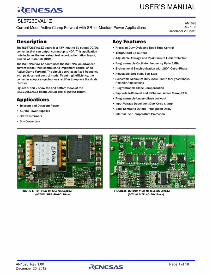
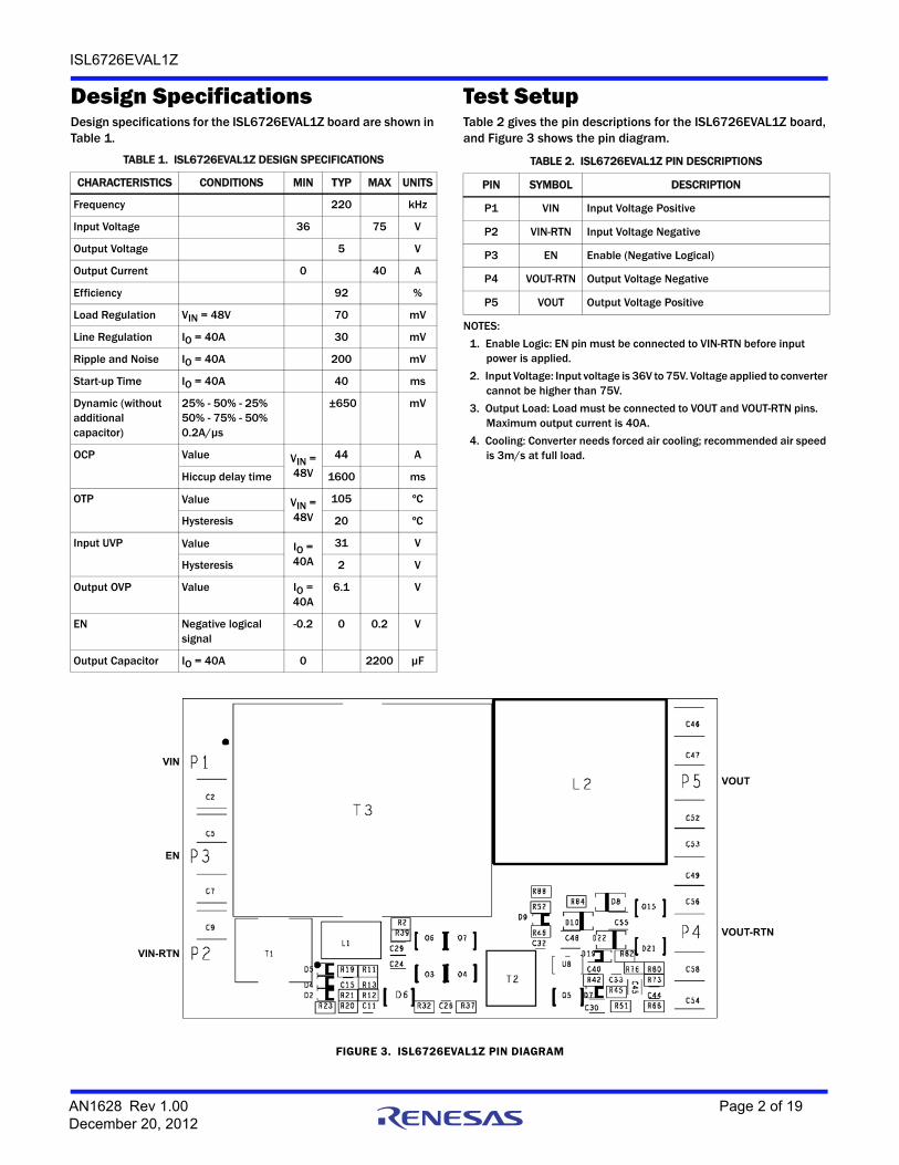
USER’S MANUAL AN1628 Rev 1.00 December 20, 2012 ISL6726EVAL1Z Current Mode Active Clamp Forward with SR for Medium Power Applications AN1628 Rev 1.00 Page 1 of 19 December 20, 2012 Description The ISL6726EVAL1Z board is a 48V input to 5V output DC/DC converter that can output current up to 40A. This application note includes the test setup, test report, schematics, layout, and bill of materials (BOM). The ISL6726EVAL1Z board uses the ISL6726, an advanced current mode PWM controller, to implement control of an Active Clamp Forward. The circuit operates at fixed frequency with peak current control mode. To get high efficiency, the converter adopts a synchronous rectifier to replace the diode rectifier. Figures 1 and 2 show top and bottom views of the ISL6726EVAL1Z board. Actual size is 40x60x16mm. Applications • Telecom and Datacom Power • AC/DC Power Supplies • DC Transformers • Bus Converters Key Features • Precision Duty Cycle and Dead-Time Control • 180μA Start-up Current • Adjustable Average and Peak Current Limit Protection • Programmable Oscillator Frequency Up to 1MHz • Bi-directional Synchronization with 180° Out-of-Phase • Adjustable Soft-Start, Soft-Stop • Selectable Minimum Duty Cycle Clamp for Synchronous Rectifier Applications • Programmable Slope Compensation • Supports N-Channel and P-Channel Active Clamp FETs • Programmable Undervoltage Lock-out • Input Voltage Dependent Duty Cycle Clamp • 35ns Control to Output Propagation Delay • Internal Over-Temperature Protection FIGURE 1. TOP VIEW OF ISL6726EVAL1Z (ACTUAL SIZE: 40x60x16mm) FIGURE 2. BOTTOM VIEW OF ISL6726EVAL1Z (ACTUAL SIZE: 40x60x16mm)
Transcript of Description Key Features - Intersil · ISL6726EVAL1Z Current Mode Active Clamp Forward with SR for...
USER’S MANUAL
AN1628Rev 1.00
December 20, 2012
ISL6726EVAL1ZCurrent Mode Active Clamp Forward with SR for Medium Power Applications
DescriptionThe ISL6726EVAL1Z board is a 48V input to 5V output DC/DC converter that can output current up to 40A. This application note includes the test setup, test report, schematics, layout, and bill of materials (BOM).
The ISL6726EVAL1Z board uses the ISL6726, an advanced current mode PWM controller, to implement control of an Active Clamp Forward. The circuit operates at fixed frequency with peak current control mode. To get high efficiency, the converter adopts a synchronous rectifier to replace the diode rectifier.
Figures 1 and 2 show top and bottom views of the ISL6726EVAL1Z board. Actual size is 40x60x16mm.
Applications• Telecom and Datacom Power
• AC/DC Power Supplies
• DC Transformers
• Bus Converters
Key Features• Precision Duty Cycle and Dead-Time Control
• 180µA Start-up Current
• Adjustable Average and Peak Current Limit Protection
• Programmable Oscillator Frequency Up to 1MHz
• Bi-directional Synchronization with 180° Out-of-Phase
• Adjustable Soft-Start, Soft-Stop
• Selectable Minimum Duty Cycle Clamp for Synchronous Rectifier Applications
• Programmable Slope Compensation
• Supports N-Channel and P-Channel Active Clamp FETs
• Programmable Undervoltage Lock-out
• Input Voltage Dependent Duty Cycle Clamp
• 35ns Control to Output Propagation Delay
• Internal Over-Temperature Protection
FIGURE 1. TOP VIEW OF ISL6726EVAL1Z(ACTUAL SIZE: 40x60x16mm)
FIGURE 2. BOTTOM VIEW OF ISL6726EVAL1Z(ACTUAL SIZE: 40x60x16mm)
AN1628 Rev 1.00 Page 1 of 19December 20, 2012
ISL6726EVAL1Z
Design SpecificationsDesign specifications for the ISL6726EVAL1Z board are shown in Table 1.
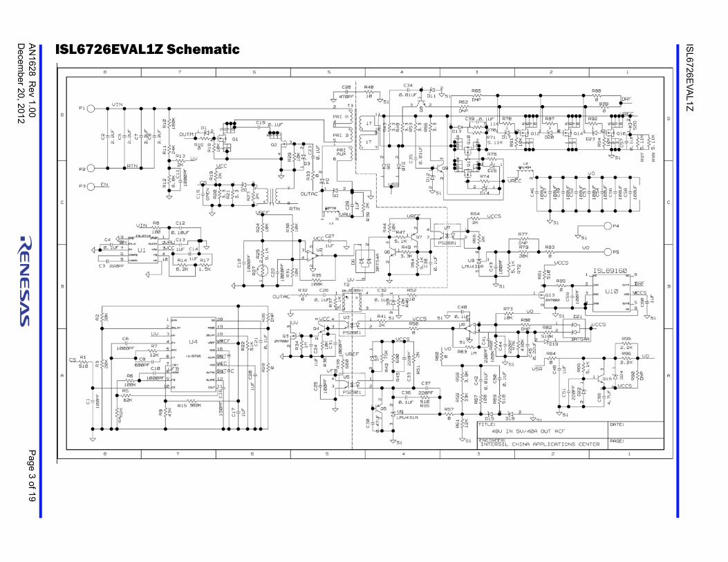
Test SetupTable 2 gives the pin descriptions for the ISL6726EVAL1Z board, and Figure 3 shows the pin diagram.
TABLE 1. ISL6726EVAL1Z DESIGN SPECIFICATIONS
CHARACTERISTICS CONDITIONS MIN TYP MAX UNITS
Frequency 220 kHz
Input Voltage 36 75 V
Output Voltage 5 V
Output Current 0 40 A
Efficiency 92 %
Load Regulation VIN = 48V 70 mV
Line Regulation IO = 40A 30 mV
Ripple and Noise IO = 40A 200 mV
Start-up Time IO = 40A 40 ms
Dynamic (without additional capacitor)
25% - 50% - 25%50% - 75% - 50%0.2A/µs
±650 mV
OCP Value VIN = 48V
44 A
Hiccup delay time 1600 ms
OTP Value VIN = 48V
105 ºC
Hysteresis 20 ºC
Input UVP Value IO = 40A
31 V
Hysteresis 2 V
Output OVP Value IO = 40A
6.1 V
EN Negative logical signal
-0.2 0 0.2 V
Output Capacitor IO = 40A 0 2200 µF
TABLE 2. ISL6726EVAL1Z PIN DESCRIPTIONS
PIN SYMBOL DESCRIPTION
P1 VIN Input Voltage Positive
P2 VIN-RTN Input Voltage Negative
P3 EN Enable (Negative Logical)
P4 VOUT-RTN Output Voltage Negative
P5 VOUT Output Voltage Positive
NOTES:
1. Enable Logic: EN pin must be connected to VIN-RTN before input power is applied.
2. Input Voltage: Input voltage is 36V to 75V. Voltage applied to converter cannot be higher than 75V.
3. Output Load: Load must be connected to VOUT and VOUT-RTN pins. Maximum output current is 40A.
4. Cooling: Converter needs forced air cooling; recommended air speed is 3m/s at full load.
FIGURE 3. ISL6726EVAL1Z PIN DIAGRAM
VIN
EN
VIN-RTN
VOUT-RTN
VOUT
AN1628 Rev 1.00 Page 2 of 19December 20, 2012
AN
16
28R
ev 1.0
0P
age 3 of 1
9D
ece
mb
er 2
0, 2
012
ISL6
726
EV
AL1
Z
ISL6726EVAL1Z Schematic
ISL6726EVAL1Z
SilkscreensFigures 4 and 5 show silkscreen images of the ISL6726EVAL1Z board top and bottom views.
FIGURE 4. ISL6726EVAL1Z TOP VIEW
FIGURE 5. ISL6726EVAL1Z BOTTOM VIEW
AN1628 Rev 1.00 Page 4 of 19December 20, 2012

ISL6726EVAL1Z
Bill of MaterialsPART NUMBER REF DES QTY VALUE MANUFACTURER
LMV431 U6, U9 2 NATIONAL SEMI
2N7002 Q3, Q13 2 ZETEX
BAT54A D6, D21 2 ZETEX
BC857 Q7, Q5 2 PNP Philips
BC847 Q4, Q6, Q8, Q9, Q15 5 NPN Philips
P0770.224NL L1 1 220µH PULSE
PA1294.910NL L2 1 0.91µH PULSE
ISL6719 U1 1 INTERSIL
ISL6726 U4 1 INTERSIL
12103C225KAT2A C2, C5, C7, C9 4 2.2µF/100V AVX
1808N471K202N C28 1 470pF/2kV NOVACAP
1N4148W-V D8, D10, D13, D25 4 VISHAY
76C100P P1-P5 5 GENERIC
BZT52C7V5 D22 1 DIODES
BZT52C18 D11,D12, 2 DIODES
C1005C0G1H221J C3, C37, C41, C44, C51 6 220pF TDK
C1608X7R1C105K C13, C14, C27, C29, C60, C17, C20, C24 8 1µF TDK
C1608X7R1C474K C30 1 0.47µF TDK
C3216X7R2E104K C19 1 0.1µF TDK
BAS516 D1-D5, D7, D9, D14-D20, D23, D24 16 DIODES
EL5111 U2, U8 2 INTERSIL
ERTJ1VR682J R27 1 6.8k PANASONIC
GRM31CR72A104KW03L C12 1 0.10UF MuRata
H1044-00101-50V5 C1, C25, C43, C59 4 100pF GENERIC
H1044-00102-50V10 C6, C10, C11, C18, C22, C31 6 1000pF GENERIC
H1044-00103-16V10 C42 1 0.01µF GENERIC
H1044-00104-16V10 C4, C21, C26, C32, C36, C38, C40, C50, C23 9 0.1µF GENERIC
H1044-00151-50V5 C16 1 150pF GENERIC
H1044-00681-50V10 C8 1 680pF GENERIC
H1044-OPEN C15, C33 2 OPEN GENERIC
H1045-00103-50V10 C34, C35 2 0.01µF GENERIC
H1045-00224-16V10 C45 1 0.22µF GENERIC
H1046-00104-100V10 C39, C57 2 0.1µF GENERIC
H1046-00105-50V8020 C48 1 1µF GENERIC
H1046-00475-10V20 C55 1 4.7µF GENERIC
H1082-00107-6R3V20 C46, C47, C49, C52-C54, C56, C58 8 100µF GENERIC
H2510-003R3-1/16W5 R20, R21, R52 2 3.3 GENERIC
H2510-00R00-1/16W R28, R32, R50, R57, R60, R83-R85, R88, R89 10 0 GENERIC
H2510-01000-1/16W1 R67 1 100 GENERIC
AN1628 Rev 1.00 Page 5 of 19December 20, 2012

ISL6726EVAL1Z
H2510-01002-1/16W5 R18, R24, R29-R31, R36, R44, R46, R73, R91, R94 11 10k GENERIC
H2510-01003-1/16W1 R6, R35, R68 3 100k GENERIC
H2510-01004-1/16W1 R34, R63 2 1M GENERIC
H2510-01202-1/16W1 R7, R61 2 12k GENERIC
H2510-01501-1/16W1 R17 1 1.5k GENERIC
H2510-01803-1/16W5 R10 1 180k GENERIC
H2510-02001-1/16W5 R13, R19, R23, R39, R41, R51, R64, R66 8 2k GENERIC
H2510-02002-1/16W5 R3, R79 2 20k GENERIC
H2510-02402-1/16W5 R11 1 24k GENERIC
H2510-03002-1/16W1 R2 1 30k GENERIC
H2510-03003-1/16W5 R15 1 300k GENERIC
H2510-03301-1/16W5 R49 1 3.3k GENERIC
H2510-03302-1/16W1 R59 1 33k GENERIC
H2510-03901-1/16W5 R58 1 3.9k GENERIC
H2510-04302-1/16W1 R9 1 43k GENERIC
H2510-04303-1/16W1 R76 1 430k GENERIC
H2510-05100-1/16W1 R1, R55, R69, R81 4 510 GENERIC
H2510-05101-1/16W1 R37, R47, R54, R72, R86 5 5.1k GENERIC
H2510-05102-1/16W5 R22 1 51k GENERIC
H2510-05103-1/16W1 R82 1 510k GENERIC
H2510-06202-1/16W1 R4, R5 2 62k GENERIC
H2510-06800-1/16W5 R38, R45 2 680 GENERIC
H2510-06801-1/16W5 R12 1 6.8k GENERIC
H2510-07502-1/16W5 R42 1 75k GENERIC
H2510-08201-1/16W1 R14 1 8.2k GENERIC
H2510-09101-1/16W1 R25 1 9.1k GENERIC
H2510-DNP-DNP-1 R26, R62, R65, R77, R80, R90 6 DNP GENERIC
H2511-00010-1/10W1 R74, R75, R78, R87, R92 5 1 GENERIC
H2511-00100-1/16W1 R40 1 10 GENERIC
H2511-00R00-1/16W1 R16, R33 2 1 GENERIC
H2512-003R3-1/10W1 R43, R48, R53, R56 4 3.6 GENERIC
H2513-01000-1/8W1 R8 1 100 GENERIC
H2513-02201-1/8W1 R95, R96 2 2.2k GENERIC
H2513-05111-1/8W1 R70, R71, R97, R99 4 5.1k GENERIC
PA2001NL T2 1 PULSE
PG1019NL T3 1 PULSE
PA1005.050 T1 1 PULSE
PS2801-1-A U3, U5, U7 3 NEC
SI7738 Q1 1 VISHAY
Bill of Materials (Continued)
PART NUMBER REF DES QTY VALUE MANUFACTURER
AN1628 Rev 1.00 Page 6 of 19December 20, 2012
ISL6726EVAL1Z
SIR438DP Q10, Q11 2 VISHAY
NTMFS4852N Q12, Q14, Q16 3 ONSEMI
Si3437DV Q2 1 VISHAY
ISL89160 U10 1 INTERSIL
TOTAL 218
Bill of Materials (Continued)
PART NUMBER REF DES QTY VALUE MANUFACTURER
AN1628 Rev 1.00 Page 7 of 19December 20, 2012

ISL6726EVAL1Z
Test ResultsProvided here are reports for the following tests of the ISL6726EVAL1Z board: efficiency, load regulation, start-up and shut-down, capacitive load start-up and shut-down (with 2200µF extra capacitor), protection function, ripple and noise, and dynamic response.
Efficiency Test
.
TABLE 3. EFFICIENCY AT VIN = 36V
VIN (V) IIN (A) PIN (W) VO (V) IO (A) PO (W)
36.070 0.505 18.2154 5.0243 3.006 15.1066 0.82993
36.054 0.941 33.9268 5.0235 6.036 30.3218 0.89374
36.038 1.374 49.5162 5.0270 9.029 45.3888 0.91664
36.025 1.806 65.0612 5.0243 12.000 60.2916 0.92669
36.012 2.234 80.4508 5.0140 14.952 74.9693 0.93187
35.998 2.681 96.5106 5.0110 17.990 90.1479 0.93407
35.984 3.312 112.702 5.007 21.025 105.272 0.93408
35.970 3.587 129.024 5.006 24.051 120.399 0.93315
35.955 4.046 145.474 5.005 27.039 135.330 0.93027
35.940 4.510 162.089 5.0013 30.048 150.279 0.92714
35.925 4.979 178.871 4.998 33.045 165.159 0.92334
35.909 5.455 195.884 4.996 36.036 180.036 0.91910
35.888 6.106 219.132 4.990 40.000 199.600 0.91087
94
76
79
73
85
88
82
91
97
3 3630 391812 2460 33272115970
PE
RC
EN
T (
%)
FIGURE 6. MAXIMUM EFFICIENCY ~93.4% @ 48V/21A,OR 36V/20A
VIN = 36V
VIN = 48V
VIN = 60VVIN = 75V
IOUT (A)
TABLE 4. EFFICIENCY AT VIN = 48V
VIN (V) IIN (A) PIN (W) VO (V) IO (A) PO (W)
48.070 0.392 18.8434 5.0362 3.0057 15.1373 0.80332
48.060 0.714 34.3148 5.0395 6.0210 30.3428 0.88425
48.048 1.039 49.9219 5.0320 9.0150 45.3635 0.90869
48.039 1.359 65.2850 5.0260 11.975 60.1864 0.92190
48.029 1.690 81.1690 5.0240 15.018 75.4504 0.92955
48.020 2.022 97.0964 5.0230 18.020 90.5145 0.93221
48.010 2.355 113.064 5.0190 21.041 105.605 0.93403
48.001 2.690 129.120 5.0134 24.046 120.552 0.93364
47.990 3.028 145.314 5.0083 27.054 135.495 0.93243
47.980 3.369 161.645 5.0036 30.058 150.398 0.93043
47.970 3.715 178.209 4.9985 33.060 165.250 0.92729
47.959 4.064 194.905 4.9930 36.067 180.083 0.92395
47.945 4.538 217.574 4.9850 40.065 199.724 0.91796
TABLE 5. EFFICIENCY AT VIN = 60V
VIN (V) IIN (A) PIN (W) VO (V) IO (A) PO (W)
60.069 0.326 19.5825 5.0410 3.001 15.1321 0.77273
60.061 0.583 35.0156 5.0470 6.007 30.3199 0.86590
60.051 0.845 50.7431 5.0400 9.015 45.4356 0.89540
60.043 1.106 66.4076 5.0360 12.020 60.5327 0.91153
60.036 1.370 82.2493 5.0385 15.024 75.6984 0.92035
60.028 1.635 98.1458 5.0365 18.031 90.8131 0.92529
60.021 1.901 114.100 5.0336 21.037 105.892 0.92806
60.013 2.169 130.168 5.0291 24.046 120.930 0.92903
60.006 2.438 146.295 5.0238 27.054 135.914 0.92904
59.997 2.709 162.532 5.0178 30.058 150.825 0.92797
59.989 2.983 178.947 5.0100 33.060 165.631 0.92558
59.981 3.259 195.478 5.0040 36.065 180.469 0.92322
59.970 3.635 217.991 4.9970 40.065 200.205 0.91841
AN1628 Rev 1.00 Page 8 of 19December 20, 2012
ISL6726EVAL1Z
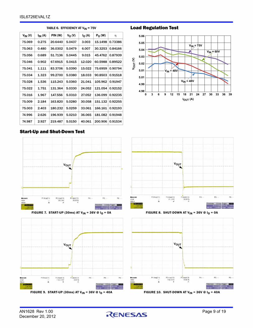
Load Regulation TestTABLE 6. EFFICIENCY AT VIN = 75V
VIN (V) IIN (A) PIN (W) VO (V) IO (A) PO (W)
75.069 0.275 20.6440 5.0437 3.003 15.1498 0.73386
75.063 0.480 36.0302 5.0479 6.007 30.3253 0.84166
75.056 0.689 51.7136 5.0445 9.015 45.4762 0.87939
75.046 0.902 67.6915 5.0415 12.020 60.5988 0.89522
75.041 1.111 83.3706 5.0390 15.022 75.6959 0.90794
75.034 1.323 99.2700 5.0380 18.033 90.8503 0.91518
75.028 1.536 115.243 5.0360 21.041 105.962 0.91947
75.022 1.751 131.364 5.0330 24.052 121.054 0.92152
75.016 1.967 147.556 5.0310 27.052 136.099 0.92235
75.009 2.184 163.820 5.0280 30.058 151.132 0.92255
75.003 2.403 180.232 5.0259 33.061 166.161 0.92193
74.996 2.626 196.939 5.0210 36.065 181.082 0.91948
74.987 2.927 219.487 5.0150 40.061 200.906 0.91534
5.05
4.99
5.01
4.98
5.02
5.03
5.01
5.04
5.06
3 3630 391812 2460 332721159
VIN = 48V
VIN = 75V
VIN = 60V
VIN = 48V
IOUT (A)
VO
UT (
V)
Start-Up and Shut-Down Test
FIGURE 7. START-UP (30ms) AT VIN = 36V @ IO = 0A FIGURE 8. SHUT-DOWN AT VIN = 36V @ IO = 0A
FIGURE 9. START-UP (30ms) AT VIN = 36V @ IO = 40A FIGURE 10. SHUT-DOWN AT VIN = 36V @ IO = 40A
VOUTVOUT
VOUTVOUT
AN1628 Rev 1.00 Page 9 of 19December 20, 2012
ISL6726EVAL1Z
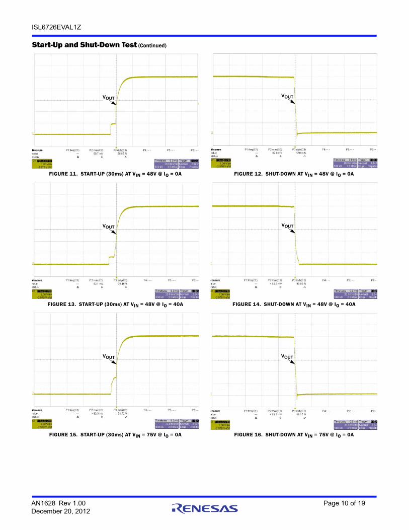
FIGURE 11. START-UP (30ms) AT VIN = 48V @ IO = 0A FIGURE 12. SHUT-DOWN AT VIN = 48V @ IO = 0A
FIGURE 13. START-UP (30ms) AT VIN = 48V @ IO = 40A FIGURE 14. SHUT-DOWN AT VIN = 48V @ IO = 40A
FIGURE 15. START-UP (30ms) AT VIN = 75V @ IO = 0A FIGURE 16. SHUT-DOWN AT VIN = 75V @ IO = 0A
Start-Up and Shut-Down Test (Continued)
VOUTVOUT
VOUT VOUT
VOUT VOUT
AN1628 Rev 1.00 Page 10 of 19December 20, 2012
ISL6726EVAL1Z
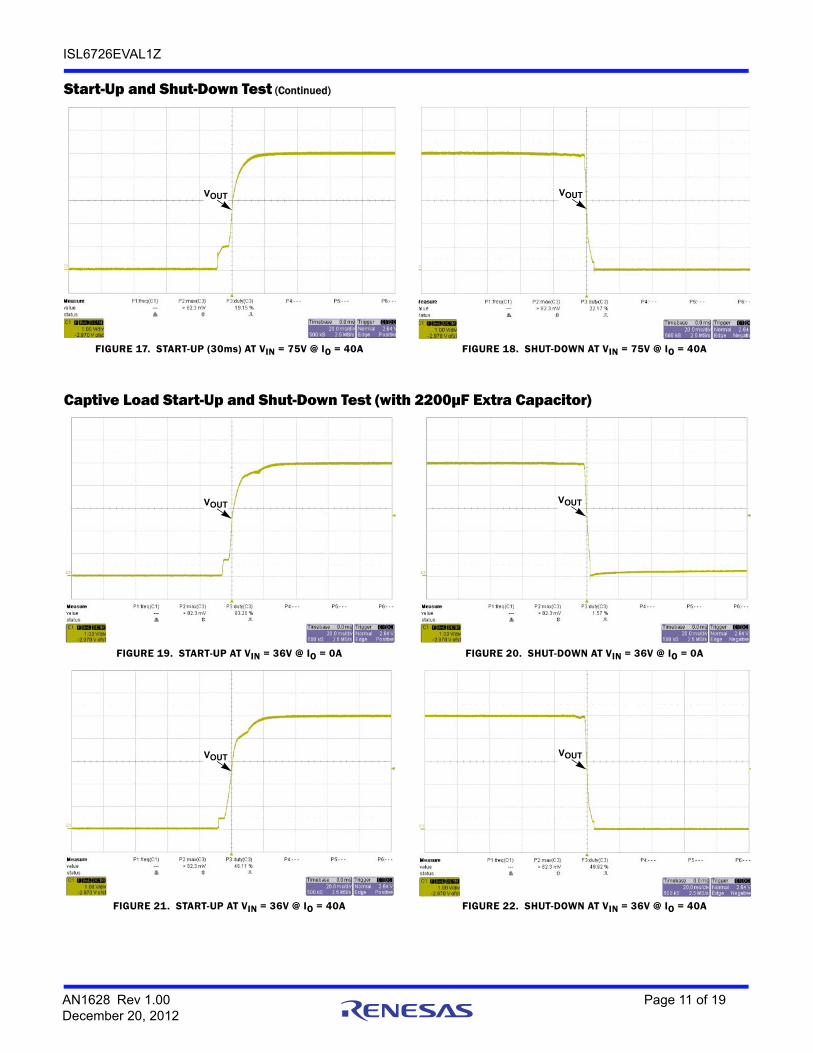
FIGURE 17. START-UP (30ms) AT VIN = 75V @ IO = 40A FIGURE 18. SHUT-DOWN AT VIN = 75V @ IO = 40A
Start-Up and Shut-Down Test (Continued)
VOUT VOUT
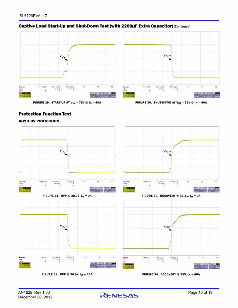
Captive Load Start-Up and Shut-Down Test (with 2200µF Extra Capacitor)
FIGURE 19. START-UP AT VIN = 36V @ IO = 0A FIGURE 20. SHUT-DOWN AT VIN = 36V @ IO = 0A
FIGURE 21. START-UP AT VIN = 36V @ IO = 40A FIGURE 22. SHUT-DOWN AT VIN = 36V @ IO = 40A
VOUT VOUT
VOUT VOUT
AN1628 Rev 1.00 Page 11 of 19December 20, 2012
ISL6726EVAL1Z
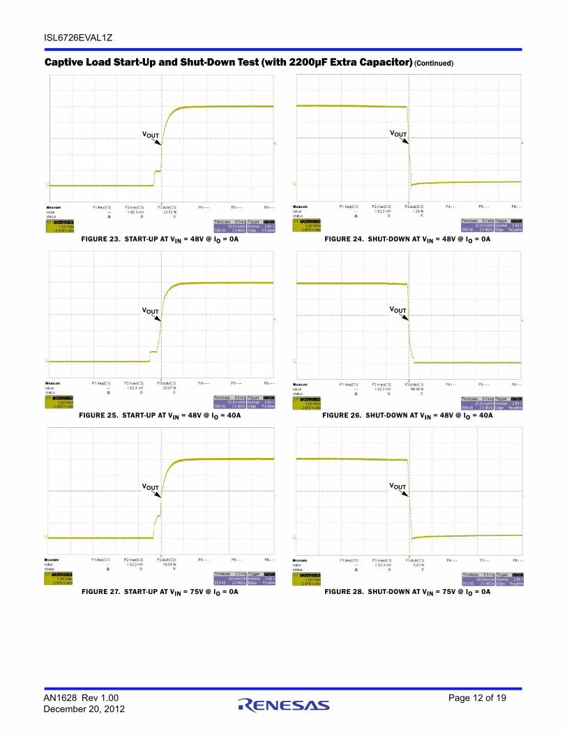
FIGURE 23. START-UP AT VIN = 48V @ IO = 0A FIGURE 24. SHUT-DOWN AT VIN = 48V @ IO = 0A
FIGURE 25. START-UP AT VIN = 48V @ IO = 40A FIGURE 26. SHUT-DOWN AT VIN = 48V @ IO = 40A
FIGURE 27. START-UP AT VIN = 75V @ IO = 0A FIGURE 28. SHUT-DOWN AT VIN = 75V @ IO = 0A
Captive Load Start-Up and Shut-Down Test (with 2200µF Extra Capacitor) (Continued)
VOUT VOUT
VOUT VOUT
VOUT VOUT
AN1628 Rev 1.00 Page 12 of 19December 20, 2012
ISL6726EVAL1Z
FIGURE 29. START-UP AT VIN = 75V @ IO = 40A FIGURE 30. SHUT-DOWN AT VIN = 75V @ IO = 40A
Captive Load Start-Up and Shut-Down Test (with 2200µF Extra Capacitor) (Continued)
VOUT VOUT
Protection Function TestINPUT UV PROTECTION
FIGURE 31. UVP @ 30.7V, IO = 0A FIGURE 32. RECOVERY @ 33.1V, IO = 0A
FIGURE 33. UVP @ 30.9V, IO = 40A FIGURE 34. RECOVERY @ 33V, IO = 40A
VOUT VOUT
VOUT VOUT
AN1628 Rev 1.00 Page 13 of 19December 20, 2012
ISL6726EVAL1Z
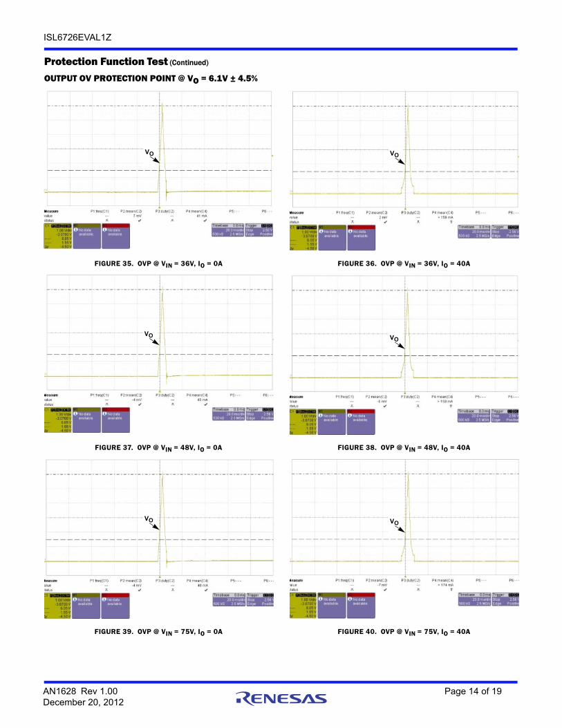
OUTPUT OV PROTECTION POINT @ VO = 6.1V ± 4.5%
FIGURE 35. OVP @ VIN = 36V, IO = 0A FIGURE 36. OVP @ VIN = 36V, IO = 40A
FIGURE 37. OVP @ VIN = 48V, IO = 0A FIGURE 38. OVP @ VIN = 48V, IO = 40A
FIGURE 39. OVP @ VIN = 75V, IO = 0A FIGURE 40. OVP @ VIN = 75V, IO = 40A
Protection Function Test (Continued)
VO VO
VO VO
VO VO
AN1628 Rev 1.00 Page 14 of 19December 20, 2012
ISL6726EVAL1Z
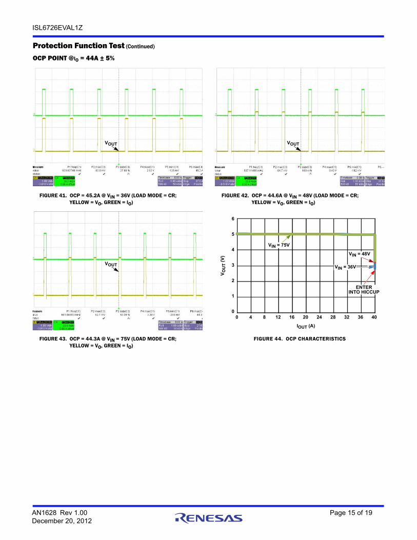
OCP POINT @IO = 44A ± 5%
FIGURE 41. OCP = 45.2A @ VIN = 36V (LOAD MODE = CR;YELLOW = VO, GREEN = IO)
FIGURE 42. OCP = 44.6A @ VIN = 48V (LOAD MODE = CR;YELLOW = VO, GREEN = IO)
FIGURE 43. OCP = 44.3A @ VIN = 75V (LOAD MODE = CR;YELLOW = VO, GREEN = IO)
FIGURE 44. OCP CHARACTERISTICS
Protection Function Test (Continued)
VOUT VOUT
VOUT
0
1
2
3
4
5
6
0 4 8 12 16 20 24 28 32 36 40
VIN = 36V
VIN = 48V
VIN = 75V
ENTERINTO HICCUP
IOUT (A)
VO
UT (
V)
AN1628 Rev 1.00 Page 15 of 19December 20, 2012

ISL6726EVAL1Z
SHORT TEST
FIGURE 45. IO OVERSHOOT, SHORT @ VIN = 36V, IO = 40A FIGURE 46. IO OVERSHOOT, SHORT @ VIN = 48V, IO = 40A
FIGURE 47. IO OVERSHOOT, SHORT @ VIN = 75V, IO = 40A
FIGURE 48. START-UP @ OUTPUT TERMINAL SHORT, VIN = 48V FIGURE 49. START-UP @ OUTPUT TERMINAL SHORT, VIN = 75V
Protection Function Test (Continued)
VOUT VOUT
VOUT
VOUT
VOUT
AN1628 Rev 1.00 Page 16 of 19December 20, 2012
ISL6726EVAL1Z
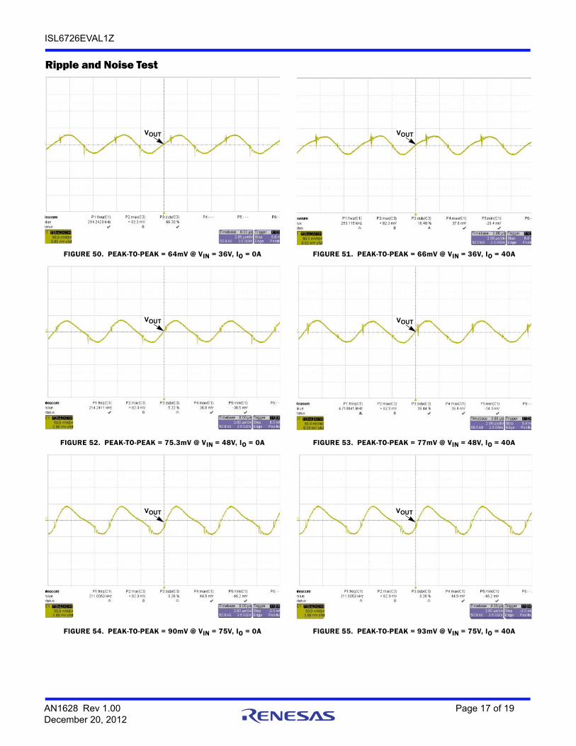
Ripple and Noise Test
FIGURE 50. PEAK-TO-PEAK = 64mV @ VIN = 36V, IO = 0A FIGURE 51. PEAK-TO-PEAK = 66mV @ VIN = 36V, IO = 40A
FIGURE 52. PEAK-TO-PEAK = 75.3mV @ VIN = 48V, IO = 0A FIGURE 53. PEAK-TO-PEAK = 77mV @ VIN = 48V, IO = 40A
FIGURE 54. PEAK-TO-PEAK = 90mV @ VIN = 75V, IO = 0A FIGURE 55. PEAK-TO-PEAK = 93mV @ VIN = 75V, IO = 40A
VOUT VOUT
VOUT VOUT
VOUT VOUT
AN1628 Rev 1.00 Page 17 of 19December 20, 2012
ISL6726EVAL1Z
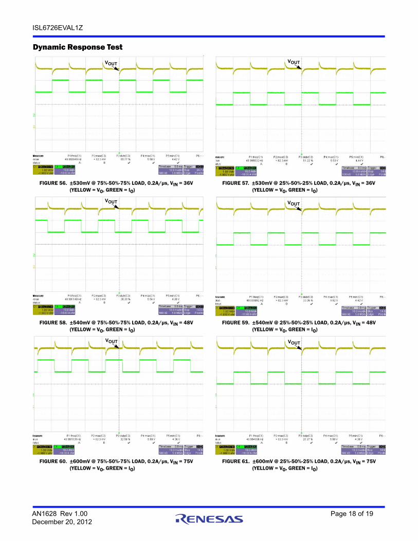
Dynamic Response Test
FIGURE 56. ±530mV @ 75%-50%-75% LOAD, 0.2A/µs, VIN = 36V(YELLOW = VO, GREEN = IO)
FIGURE 57. ±530mV @ 25%-50%-25% LOAD, 0.2A/µs, VIN = 36V(YELLOW = VO, GREEN = IO)
FIGURE 58. ±540mV @ 75%-50%-75% LOAD, 0.2A/µs, VIN = 48V(YELLOW = VO, GREEN = IO)
FIGURE 59. ±540mV @ 25%-50%-25% LOAD, 0.2A/µs, VIN = 48V(YELLOW = VO, GREEN = IO)
FIGURE 60. ±600mV @ 75%-50%-75% LOAD, 0.2A/µs, VIN = 75V(YELLOW = VO, GREEN = IO)
FIGURE 61. ±600mV @ 25%-50%-25% LOAD, 0.2A/µs, VIN = 75V(YELLOW = VO, GREEN = IO)
VOUTVOUT
VOUT VOUT
VOUT VOUT
AN1628 Rev 1.00 Page 18 of 19December 20, 2012

http://www.renesas.comRefer to "http://www.renesas.com/" for the latest and detailed information.
Renesas Electronics America Inc.1001 Murphy Ranch Road, Milpitas, CA 95035, U.S.A.Tel: +1-408-432-8888, Fax: +1-408-434-5351Renesas Electronics Canada Limited9251 Yonge Street, Suite 8309 Richmond Hill, Ontario Canada L4C 9T3Tel: +1-905-237-2004Renesas Electronics Europe LimitedDukes Meadow, Millboard Road, Bourne End, Buckinghamshire, SL8 5FH, U.KTel: +44-1628-651-700, Fax: +44-1628-651-804Renesas Electronics Europe GmbHArcadiastrasse 10, 40472 Düsseldorf, Germany Tel: +49-211-6503-0, Fax: +49-211-6503-1327Renesas Electronics (China) Co., Ltd.Room 1709 Quantum Plaza, No.27 ZhichunLu, Haidian District, Beijing, 100191 P. R. ChinaTel: +86-10-8235-1155, Fax: +86-10-8235-7679Renesas Electronics (Shanghai) Co., Ltd.Unit 301, Tower A, Central Towers, 555 Langao Road, Putuo District, Shanghai, 200333 P. R. China Tel: +86-21-2226-0888, Fax: +86-21-2226-0999Renesas Electronics Hong Kong LimitedUnit 1601-1611, 16/F., Tower 2, Grand Century Place, 193 Prince Edward Road West, Mongkok, Kowloon, Hong KongTel: +852-2265-6688, Fax: +852 2886-9022Renesas Electronics Taiwan Co., Ltd.13F, No. 363, Fu Shing North Road, Taipei 10543, TaiwanTel: +886-2-8175-9600, Fax: +886 2-8175-9670Renesas Electronics Singapore Pte. Ltd.80 Bendemeer Road, Unit #06-02 Hyflux Innovation Centre, Singapore 339949Tel: +65-6213-0200, Fax: +65-6213-0300Renesas Electronics Malaysia Sdn.Bhd.Unit 1207, Block B, Menara Amcorp, Amcorp Trade Centre, No. 18, Jln Persiaran Barat, 46050 Petaling Jaya, Selangor Darul Ehsan, MalaysiaTel: +60-3-7955-9390, Fax: +60-3-7955-9510Renesas Electronics India Pvt. Ltd.No.777C, 100 Feet Road, HAL 2nd Stage, Indiranagar, Bangalore 560 038, IndiaTel: +91-80-67208700, Fax: +91-80-67208777Renesas Electronics Korea Co., Ltd.17F, KAMCO Yangjae Tower, 262, Gangnam-daero, Gangnam-gu, Seoul, 06265 KoreaTel: +82-2-558-3737, Fax: +82-2-558-5338
SALES OFFICES
© 2018 Renesas Electronics Corporation. All rights reserved.Colophon 7.0
(Rev.4.0-1 November 2017)
Notice
1. Descriptions of circuits, software and other related information in this document are provided only to illustrate the operation of semiconductor products and application examples. You are fully responsible for
the incorporation or any other use of the circuits, software, and information in the design of your product or system. Renesas Electronics disclaims any and all liability for any losses and damages incurred by
you or third parties arising from the use of these circuits, software, or information.
2. Renesas Electronics hereby expressly disclaims any warranties against and liability for infringement or any other claims involving patents, copyrights, or other intellectual property rights of third parties, by or
arising from the use of Renesas Electronics products or technical information described in this document, including but not limited to, the product data, drawings, charts, programs, algorithms, and application
examples.
3. No license, express, implied or otherwise, is granted hereby under any patents, copyrights or other intellectual property rights of Renesas Electronics or others.
4. You shall not alter, modify, copy, or reverse engineer any Renesas Electronics product, whether in whole or in part. Renesas Electronics disclaims any and all liability for any losses or damages incurred by
you or third parties arising from such alteration, modification, copying or reverse engineering.
5. Renesas Electronics products are classified according to the following two quality grades: “Standard” and “High Quality”. The intended applications for each Renesas Electronics product depends on the
product’s quality grade, as indicated below.
"Standard": Computers; office equipment; communications equipment; test and measurement equipment; audio and visual equipment; home electronic appliances; machine tools; personal electronic
equipment; industrial robots; etc.
"High Quality": Transportation equipment (automobiles, trains, ships, etc.); traffic control (traffic lights); large-scale communication equipment; key financial terminal systems; safety control equipment; etc.
Unless expressly designated as a high reliability product or a product for harsh environments in a Renesas Electronics data sheet or other Renesas Electronics document, Renesas Electronics products are
not intended or authorized for use in products or systems that may pose a direct threat to human life or bodily injury (artificial life support devices or systems; surgical implantations; etc.), or may cause
serious property damage (space system; undersea repeaters; nuclear power control systems; aircraft control systems; key plant systems; military equipment; etc.). Renesas Electronics disclaims any and all
liability for any damages or losses incurred by you or any third parties arising from the use of any Renesas Electronics product that is inconsistent with any Renesas Electronics data sheet, user’s manual or
other Renesas Electronics document.
6. When using Renesas Electronics products, refer to the latest product information (data sheets, user’s manuals, application notes, “General Notes for Handling and Using Semiconductor Devices” in the
reliability handbook, etc.), and ensure that usage conditions are within the ranges specified by Renesas Electronics with respect to maximum ratings, operating power supply voltage range, heat dissipation
characteristics, installation, etc. Renesas Electronics disclaims any and all liability for any malfunctions, failure or accident arising out of the use of Renesas Electronics products outside of such specified
ranges.
7. Although Renesas Electronics endeavors to improve the quality and reliability of Renesas Electronics products, semiconductor products have specific characteristics, such as the occurrence of failure at a
certain rate and malfunctions under certain use conditions. Unless designated as a high reliability product or a product for harsh environments in a Renesas Electronics data sheet or other Renesas
Electronics document, Renesas Electronics products are not subject to radiation resistance design. You are responsible for implementing safety measures to guard against the possibility of bodily injury, injury
or damage caused by fire, and/or danger to the public in the event of a failure or malfunction of Renesas Electronics products, such as safety design for hardware and software, including but not limited to
redundancy, fire control and malfunction prevention, appropriate treatment for aging degradation or any other appropriate measures. Because the evaluation of microcomputer software alone is very difficult
and impractical, you are responsible for evaluating the safety of the final products or systems manufactured by you.
8. Please contact a Renesas Electronics sales office for details as to environmental matters such as the environmental compatibility of each Renesas Electronics product. You are responsible for carefully and
sufficiently investigating applicable laws and regulations that regulate the inclusion or use of controlled substances, including without limitation, the EU RoHS Directive, and using Renesas Electronics
products in compliance with all these applicable laws and regulations. Renesas Electronics disclaims any and all liability for damages or losses occurring as a result of your noncompliance with applicable
laws and regulations.
9. Renesas Electronics products and technologies shall not be used for or incorporated into any products or systems whose manufacture, use, or sale is prohibited under any applicable domestic or foreign laws
or regulations. You shall comply with any applicable export control laws and regulations promulgated and administered by the governments of any countries asserting jurisdiction over the parties or
transactions.
10. It is the responsibility of the buyer or distributor of Renesas Electronics products, or any other party who distributes, disposes of, or otherwise sells or transfers the product to a third party, to notify such third
party in advance of the contents and conditions set forth in this document.
11. This document shall not be reprinted, reproduced or duplicated in any form, in whole or in part, without prior written consent of Renesas Electronics.
12. Please contact a Renesas Electronics sales office if you have any questions regarding the information contained in this document or Renesas Electronics products.
(Note 1) “Renesas Electronics” as used in this document means Renesas Electronics Corporation and also includes its directly or indirectly controlled subsidiaries.
(Note 2) “Renesas Electronics product(s)” means any product developed or manufactured by or for Renesas Electronics.