DESCRIPTION FEATURES - 普誠科技 - 車用與消費性IC ... · Electronic Volume Controller IC...
20
Tel: 886-2-66296288 Fax: 886-2-29174598 URL: http://www.princeton.com.tw PT2253A V2.8 - 1 - December, 2005 Electronic Volume Controller IC PT2253A DESCRIPTION PT2253A is an electronic volume controller IC utilizing CMOS Technology specially designed for use on audio equipments. It has two (2) built-in channels making it ideally suitable for mono and stereo sound applications. PT2253A provides a wide frequency response range and a very low harmonic distortion to mention a few; thereby guaranteeing a highly effective and reliable performance. FEATURES • CMOS technology • Low power consumption • Operating voltage range: Vcc=6 ~ 12V (Backup voltage is up to 4V) • 0dB to -68dB attenuation controlled by 2dB/step • 2 channels in each chip • Capable to control attenuation by a built-in oscillator and Up/Down pin • Single power supply or dual power supplies of (+) and (-) can be used • Wide frequency response range • Very low harmonic distortion • Available in 16 pin, DIP package APPLICATIONS • Audio Equipment Volume Control • Traditional VR Replacement
Transcript of DESCRIPTION FEATURES - 普誠科技 - 車用與消費性IC ... · Electronic Volume Controller IC...
Tel: 886-2-66296288 Fax: 886-2-29174598 URL: http://www.princeton.com.tw
PT2253A V2.8 - 1 - December, 2005
Electronic Volume Controller IC PT2253A
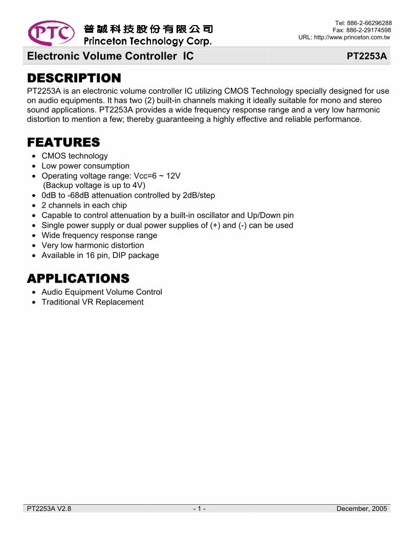
DESCRIPTION PT2253A is an electronic volume controller IC utilizing CMOS Technology specially designed for use on audio equipments. It has two (2) built-in channels making it ideally suitable for mono and stereo sound applications. PT2253A provides a wide frequency response range and a very low harmonic distortion to mention a few; thereby guaranteeing a highly effective and reliable performance.
FEATURES • CMOS technology • Low power consumption • Operating voltage range: Vcc=6 ~ 12V
(Backup voltage is up to 4V) • 0dB to -68dB attenuation controlled by 2dB/step • 2 channels in each chip • Capable to control attenuation by a built-in oscillator and Up/Down pin • Single power supply or dual power supplies of (+) and (-) can be used • Wide frequency response range • Very low harmonic distortion • Available in 16 pin, DIP package
APPLICATIONS • Audio Equipment Volume Control • Traditional VR Replacement
Tel: 886-2-66296288 Fax: 886-2-29174598 URL: http://www.princeton.com.tw
PT2253A V2.8 - 2 - December, 2005
Electronic Volume Controller IC PT2253A
BLOCK DIAGRAM
7 BITSBIDIRECTIONALSHIFT REGISTER
U/D
CK
U/D
CKINT
INT
5 BITSBIDIRECTIONALSHIFT REGISTER
AUTOINITIALIZE CIRCUIT
CONSTANT CURRENT CIRCUIT
U/D
Vcc Vss /INH
DCO
OSC OSC
CKCK
CKCK
7 B
ITS
LAT
CH
CIR
CU
IT
7 B
ITS
LAT
CH
CIR
CU
IT A-SWA-SW
A-SW
A-SW
A-SW
A-SW
A-SW
A-SW
A-SW
A-SW
A-SW
A-SW
A-SW
A-SW
A-SW
A-SW
A-SW
A-SW
A-SW
A-SW
A-SW
A-SW
A-SW
A-SW
A-SW
A-SW
R-OUT1
R-IN1
A-GND
6 B
ITS
LATC
H C
IRC
UIT
6 B
ITS
LATC
H C
IRC
UIT
CKCK
CKCK
R-IN2
R-OUT2
VccL-OUT1
L-IN1
A-GND
L-IN2
L-OUT2
Tel: 886-2-66296288 Fax: 886-2-29174598 URL: http://www.princeton.com.tw
PT2253A V2.8 - 3 - December, 2005
Electronic Volume Controller IC PT2253A
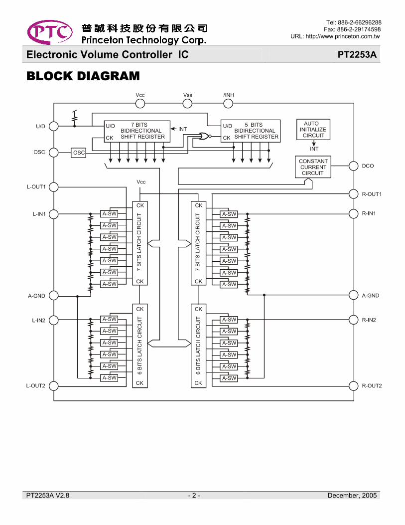
PIN CONFIGURATION
VssL-OUT1
L-IN1
Vcc
OSC
R-OUT1R-IN1
LOUT2 R-OUT2/INH
A-GND A-GND
U/D
L-IN2 R-IN2
1 162 153 144 13
8 97 106 115 12
PT2253A
DCO
PIN DESCRIPTION
Pin Name I/O Description Pin No.Vss Power Negative Power Supply 1
L-OUT1 O 10dB/Step Attenuator Output A signal applied to ‘IN’ is attenuated into 7 steps from 0dB to -60dB. 2
L-IN1 I 10dB/Step Attenuator Input 3 A-GND GND Analog Ground Pin 4 L-IN2 I 2dB/Step Attenuator Input 5
L-OUT2 O 2dB/Step Attenuator Output A signal applied to “IN” is attenuated into 5 steps from 0dB to -8dB. 6
/INH I Inhibit Terminal. At “L” level, all inputs and outputs are disabled. At “H” level, operation is normal.
7
DCO O DC Current Output Pin 8 OSC I/O RC Connecting Pin for the Oscillator 9 U/D I Attenuator Up/Down Control Pin 10
R-OUT2 O 2dB/Step Attenuator Output, same as L-OUT2. 11 R-IN2 I 2dB/Step Attenuator Input, same as L-IN2. 12
A-GND GND Analog Ground Pin 13 R-IN1 I 10dB/Step Attenuator Input, same as L-IN1. 14
R-OUT1 O 10dB/Step Attenuator Output, same as L-OUT1. 15 Vcc Power Positive Power Supply 16
Tel: 886-2-66296288 Fax: 886-2-29174598 URL: http://www.princeton.com.tw
PT2253A V2.8 - 4 - December, 2005
Electronic Volume Controller IC PT2253A
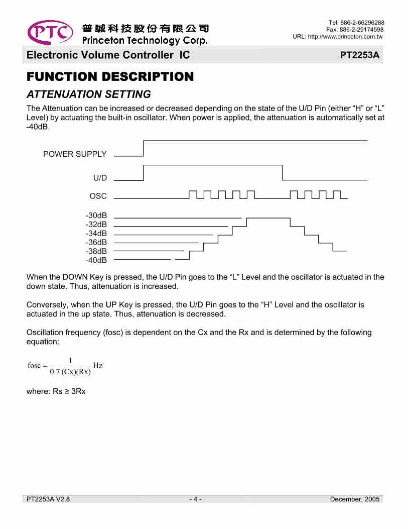
FUNCTION DESCRIPTION ATTENUATION SETTING The Attenuation can be increased or decreased depending on the state of the U/D Pin (either “H” or “L” Level) by actuating the built-in oscillator. When power is applied, the attenuation is automatically set at -40dB.
POWER SUPPLY
U/D
OSC
-30dB-32dB-34dB-36dB-38dB-40dB
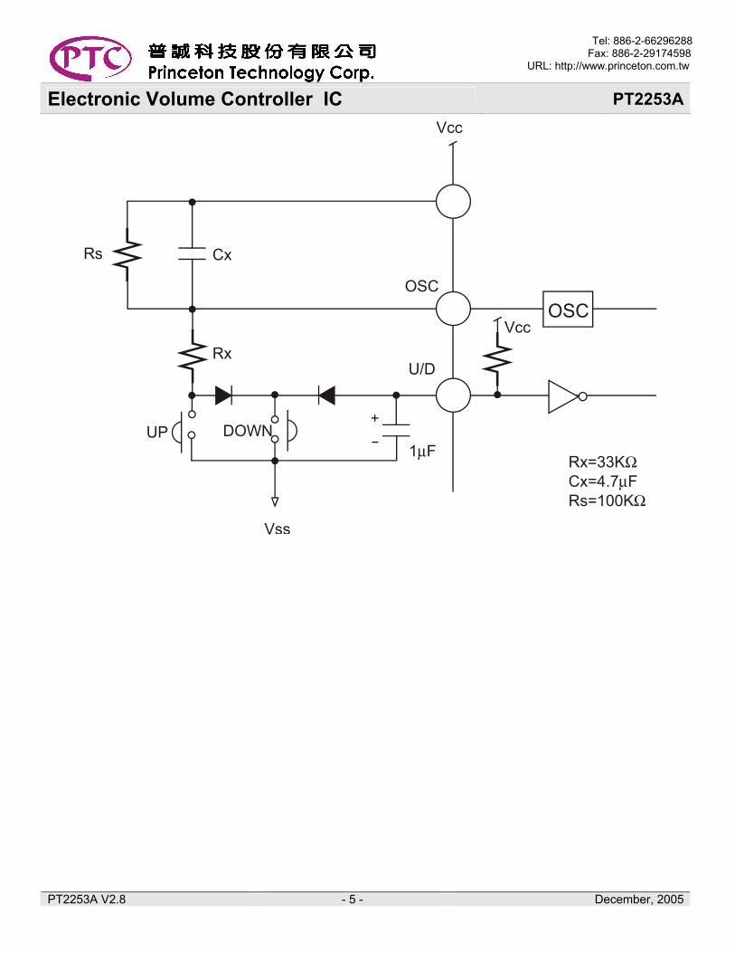
When the DOWN Key is pressed, the U/D Pin goes to the “L” Level and the oscillator is actuated in the down state. Thus, attenuation is increased. Conversely, when the UP Key is pressed, the U/D Pin goes to the “H” Level and the oscillator is actuated in the up state. Thus, attenuation is decreased. Oscillation frequency (fosc) is dependent on the Cx and the Rx and is determined by the following equation:
Hz (Cx)(Rx) 0.7
1fosc =
where: Rs ≥ 3Rx
Tel: 886-2-66296288 Fax: 886-2-29174598 URL: http://www.princeton.com.tw
PT2253A V2.8 - 5 - December, 2005
Electronic Volume Controller IC PT2253A
Rs Cx
Vcc
OSC
VccOSC
UP DOWN
Vss
1 FµRx=33KCx=4.7 FRs=100K
Ωµ
Ω
RxU/D
+
Tel: 886-2-66296288 Fax: 886-2-29174598 URL: http://www.princeton.com.tw
PT2253A V2.8 - 6 - December, 2005
Electronic Volume Controller IC PT2253A
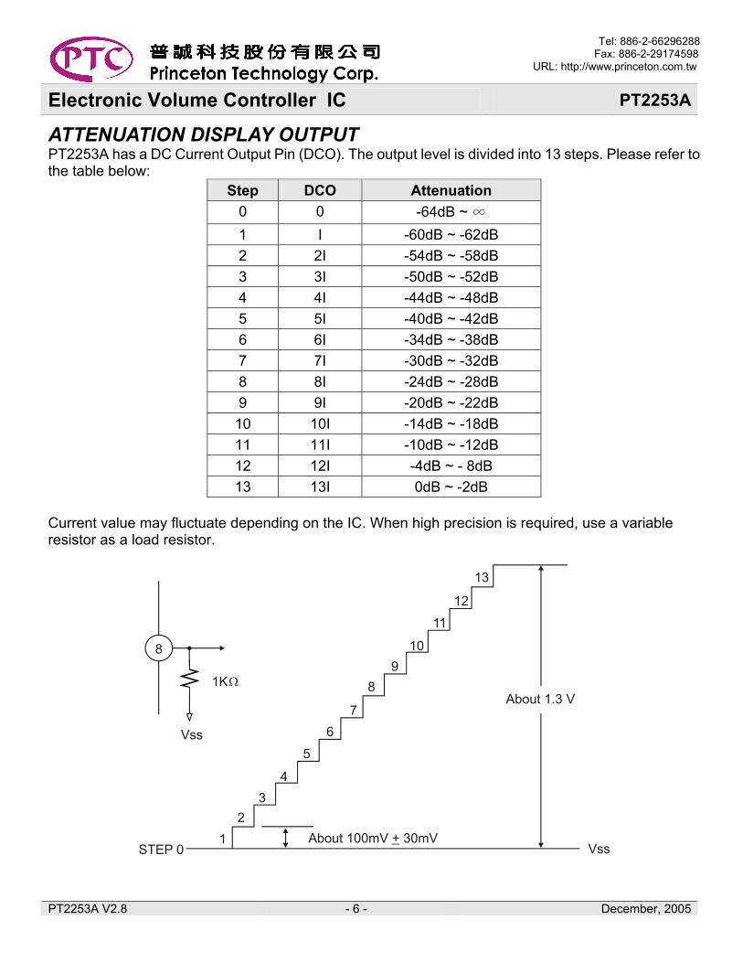
ATTENUATION DISPLAY OUTPUT PT2253A has a DC Current Output Pin (DCO). The output level is divided into 13 steps. Please refer to the table below:
Step DCO Attenuation 0 0 -64dB ~ ∞ 1 I -60dB ~ -62dB 2 2I -54dB ~ -58dB 3 3I -50dB ~ -52dB 4 4I -44dB ~ -48dB 5 5I -40dB ~ -42dB 6 6I -34dB ~ -38dB 7 7I -30dB ~ -32dB 8 8I -24dB ~ -28dB 9 9I -20dB ~ -22dB 10 10I -14dB ~ -18dB 11 11I -10dB ~ -12dB 12 12I -4dB ~ - 8dB 13 13I 0dB ~ -2dB
Current value may fluctuate depending on the IC. When high precision is required, use a variable resistor as a load resistor.
13
1211
109
8
76
5
43
2 1
STEP 0About 100mV 30mV+
About 1.3 V
8
1K
Vss
Vss
Tel: 886-2-66296288 Fax: 886-2-29174598 URL: http://www.princeton.com.tw
PT2253A V2.8 - 7 - December, 2005
Electronic Volume Controller IC PT2253A
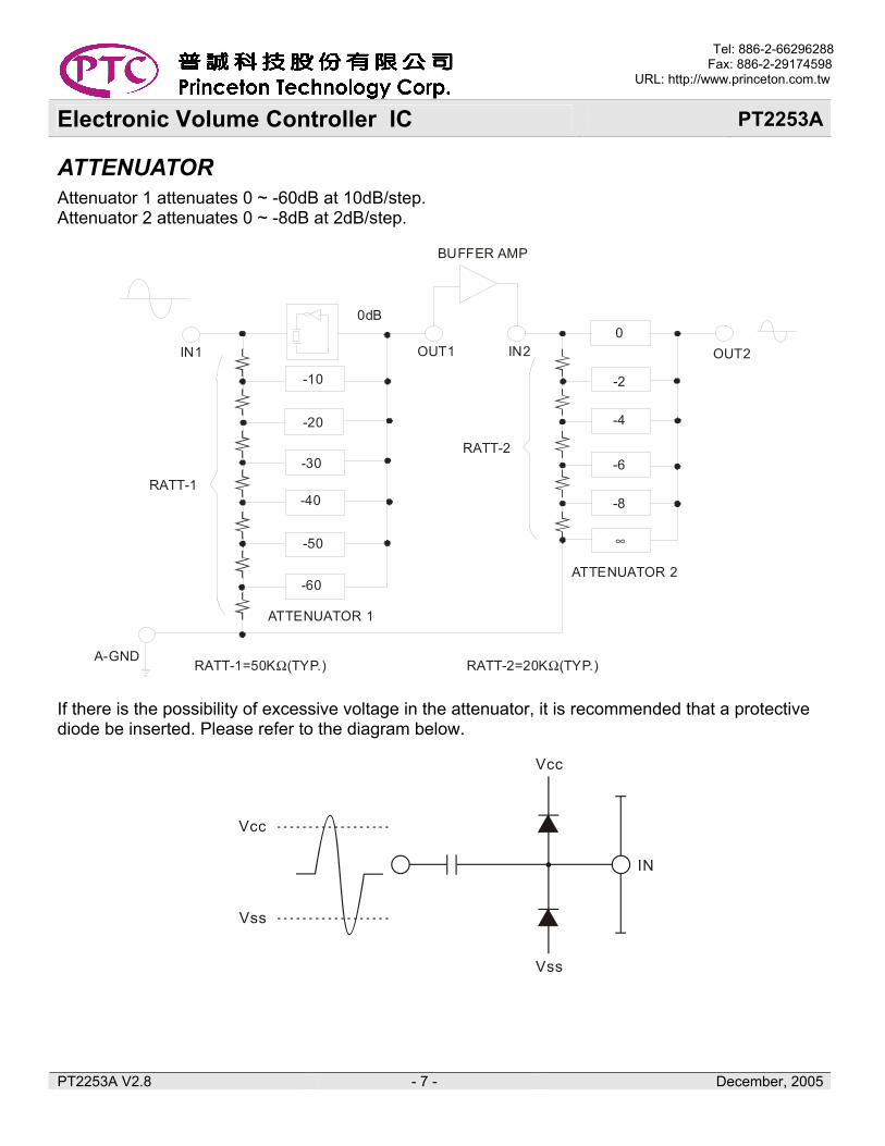
ATTENUATOR Attenuator 1 attenuates 0 ~ -60dB at 10dB/step. Attenuator 2 attenuates 0 ~ -8dB at 2dB/step.
-60
-50
-40
-30
-20
-10
ATTENUATOR 1
0dB
IN1 OUT1
RATT-1
IN2
BUFFER AMP
0
-2
-4
-6
-8
OUT2
ATTENUATOR 2
A-GNDRATT-1=50KΩ(TYP.) RATT-2=20K (TYP.)Ω
RATT-2
∞
If there is the possibility of excessive voltage in the attenuator, it is recommended that a protective diode be inserted. Please refer to the diagram below.
Vcc
Vss
IN
Vcc
Vss
Tel: 886-2-66296288 Fax: 886-2-29174598 URL: http://www.princeton.com.tw
PT2253A V2.8 - 8 - December, 2005
Electronic Volume Controller IC PT2253A
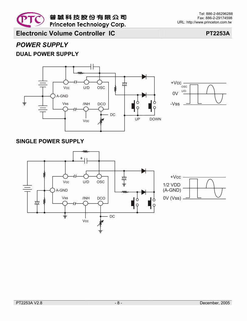
POWER SUPPLY DUAL POWER SUPPLY
A-GND
Vcc U/D OSC
DCO/INHVss
Vcc
DCUP DOWN
OSC+Vcc
0V
-Vss
U/D
SINGLE POWER SUPPLY
A-GND
Vcc U/D OSC
DCO/INHVss
VccDC
+Vcc
1/2 VDD(A-GND)
0V (Vss)
+
Tel: 886-2-66296288 Fax: 886-2-29174598 URL: http://www.princeton.com.tw
PT2253A V2.8 - 9 - December, 2005
Electronic Volume Controller IC PT2253A
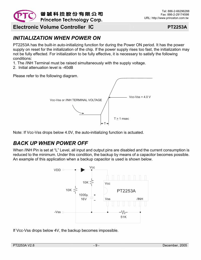
INITIALIZATION WHEN POWER ON PT2253A has the built-in auto-initializing function for during the Power ON period. It has the power supply on reset for the initialization of the chip. If the power supply rises too fast, the initialization may not be fully effected. For initialization to be fully effective, it is necessary to satisfy the following conditions: 1. The /INH Terminal must be raised simultaneously with the supply voltage. 2. Initial attenuation level is -40dB Please refer to the following diagram.
Vcc-Vss = 4.0 V
T 1 msec>T
Vcc-Vss or /INH TERMINAL VOLTAGE
Note: If Vcc-Vss drops below 4.0V, the auto-initializing function is actuated.
BACK UP WHEN POWER OFF When /INH Pin is set at “L” Level, all input and output pins are disabled and the current consumption is reduced to the minimum. Under this condition, the backup by means of a capacitor becomes possible. An example of this application when a backup capacitor is used is shown below.
PT2253A
VDDVcc
10K1000µ
16V
10K Vcc
Vss /INH
51K-Vss
+-
If Vcc-Vss drops below 4V, the backup becomes impossible.
Tel: 886-2-66296288 Fax: 886-2-29174598 URL: http://www.princeton.com.tw
PT2253A V2.8 - 10 - December, 2005
Electronic Volume Controller IC PT2253A
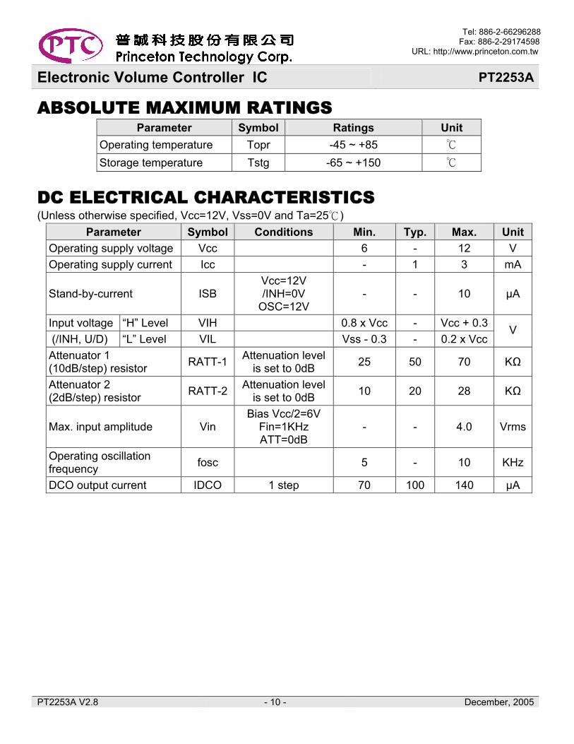
ABSOLUTE MAXIMUM RATINGS Parameter Symbol Ratings Unit
Operating temperature Topr -45 ~ +85 Storage temperature Tstg -65 ~ +150
DC ELECTRICAL CHARACTERISTICS (Unless otherwise specified, Vcc=12V, Vss=0V and Ta=25)
Parameter Symbol Conditions Min. Typ. Max. UnitOperating supply voltage Vcc 6 - 12 V Operating supply current Icc - 1 3 mA
Stand-by-current ISB Vcc=12V /INH=0V
OSC=12V - - 10 µA
Input voltage “H” Level VIH 0.8 x Vcc - Vcc + 0.3 (/INH, U/D) “L” Level VIL Vss - 0.3 - 0.2 x Vcc
V
Attenuator 1 (10dB/step) resistor RATT-1 Attenuation level
is set to 0dB 25 50 70 KΩ
Attenuator 2 (2dB/step) resistor RATT-2 Attenuation level
is set to 0dB 10 20 28 KΩ
Max. input amplitude Vin Bias Vcc/2=6V
Fin=1KHz ATT=0dB
- - 4.0 Vrms
Operating oscillation frequency fosc 5 - 10 KHz
DCO output current IDCO 1 step 70 100 140 µA
Tel: 886-2-66296288 Fax: 886-2-29174598 URL: http://www.princeton.com.tw
PT2253A V2.8 - 11 - December, 2005
Electronic Volume Controller IC PT2253A
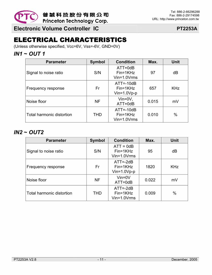
ELECTRICAL CHARACTERISTICS (Unless otherwise specified, Vcc=6V, Vss=-6V, GND=0V)
IN1 ~ OUT 1 Parameter Symbol Condition Max. Unit
Signal to noise ratio S/N ATT=0dB Fin=1KHz
Vin=1.0Vrms 97 dB
Frequency response Fr ATT=-10dB Fin=1KHz
Vin=1.0Vp-p 657 KHz
Noise floor NF Vin=0V, ATT=0dB 0.015 mV
Total harmonic distortion THD ATT=-10dB Fin=1KHz
Vin=1.0Vrms 0.010 %
IN2 ~ OUT2 Parameter Symbol Condition Max. Unit
Signal to noise ratio S/N ATT = 0dB Fin=1KHz
Vin=1.0Vrms 95 dB
Frequency response Fr ATT=-2dB Fin=1KHz
Vin=1.0Vp-p 1820 KHz
Noise floor NF Vin=0V ATT=0dB 0.022 mV
Total harmonic distortion THD ATT=-2dB Fin=1KHz
Vin=1.0Vrms 0.009 %
Tel: 886-2-66296288 Fax: 886-2-29174598 URL: http://www.princeton.com.tw
PT2253A V2.8 - 12 - December, 2005
Electronic Volume Controller IC PT2253A
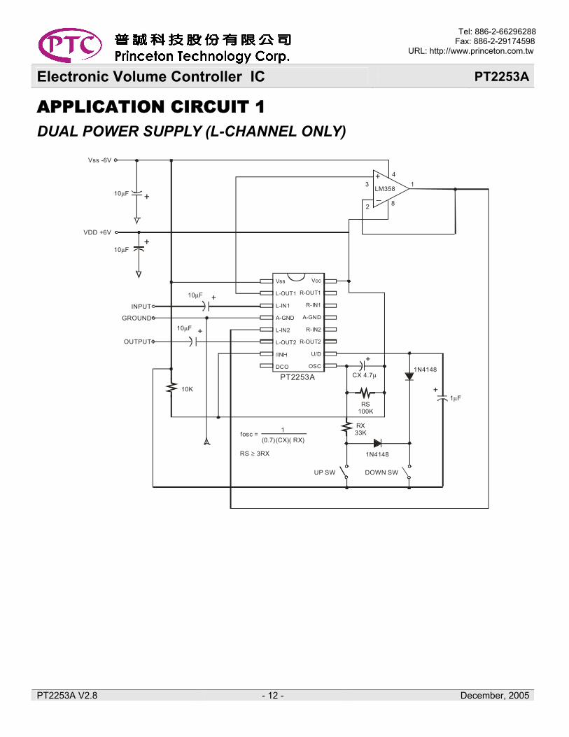
APPLICATION CIRCUIT 1 DUAL POWER SUPPLY (L-CHANNEL ONLY)
Vss
L-OUT1
L-IN1
A-GND
L-IN2
L-OUT2
/INH
DCO
Vcc
R-OUT1
R-IN1
A-GND
R-IN2
R-OUT2
U/D
OSC
PT2253A
10 Fµ +
10 Fµ +
+
CX 4.7µ
RS100K
RX33K
1N4148
+1 Fµ
1N4148
DOWN SWUP SW
INPUT
GROUND
OUTPUT
LM358
+
_10 Fµ
Vss -6V
10K
10 Fµ
VDD +6V
34
2 8
1
RS 3RX≥
+
+
fosc =1
(0.7) (CX)( RX)
Tel: 886-2-66296288 Fax: 886-2-29174598 URL: http://www.princeton.com.tw
PT2253A V2.8 - 13 - December, 2005
Electronic Volume Controller IC PT2253A
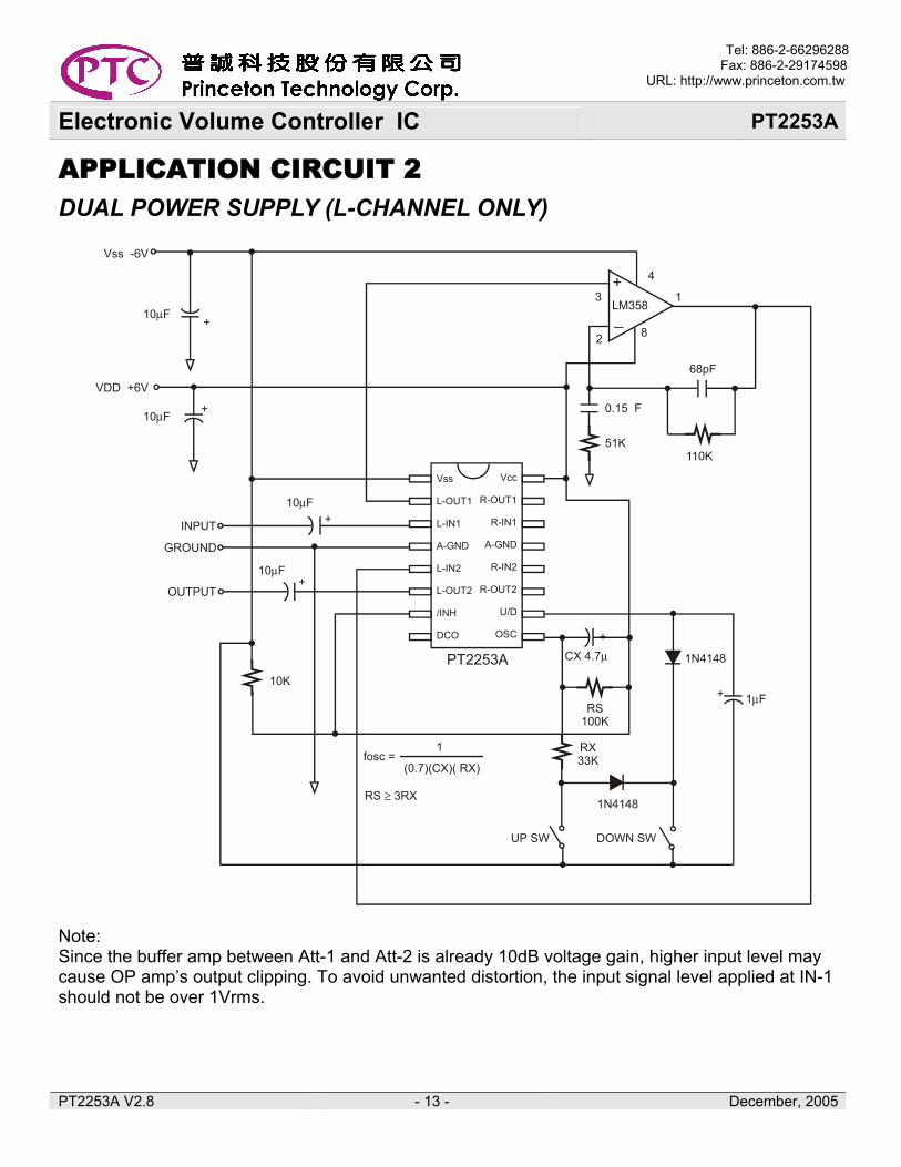
APPLICATION CIRCUIT 2 DUAL POWER SUPPLY (L-CHANNEL ONLY)
Vss
L-OUT1
L-IN1
A-GND
L-IN2
L-OUT2
/INH
DCO
Vcc
R-OUT1
R-IN1
A-GND
R-IN2
R-OUT2
U/D
OSC
PT2253A
10 Fµ
+
10 Fµ +
CX 4.7µ
RS100K
RX33K
1N4148
1 Fµ
1N4148
DOWN SWUP SW
INPUT
GROUND
OUTPUT
LM35810 Fµ
Vss -6V
10K
10 Fµ
VDD +6V
3
4
0.15 F
51K
68pF
110K
2 8
1
fosc =
+
+
RS 3RX≥
(0.7)(CX)( RX)
1
+
+
+
_
Note: Since the buffer amp between Att-1 and Att-2 is already 10dB voltage gain, higher input level may cause OP amp’s output clipping. To avoid unwanted distortion, the input signal level applied at IN-1 should not be over 1Vrms.
Tel: 886-2-66296288 Fax: 886-2-29174598 URL: http://www.princeton.com.tw
PT2253A V2.8 - 14 - December, 2005
Electronic Volume Controller IC PT2253A
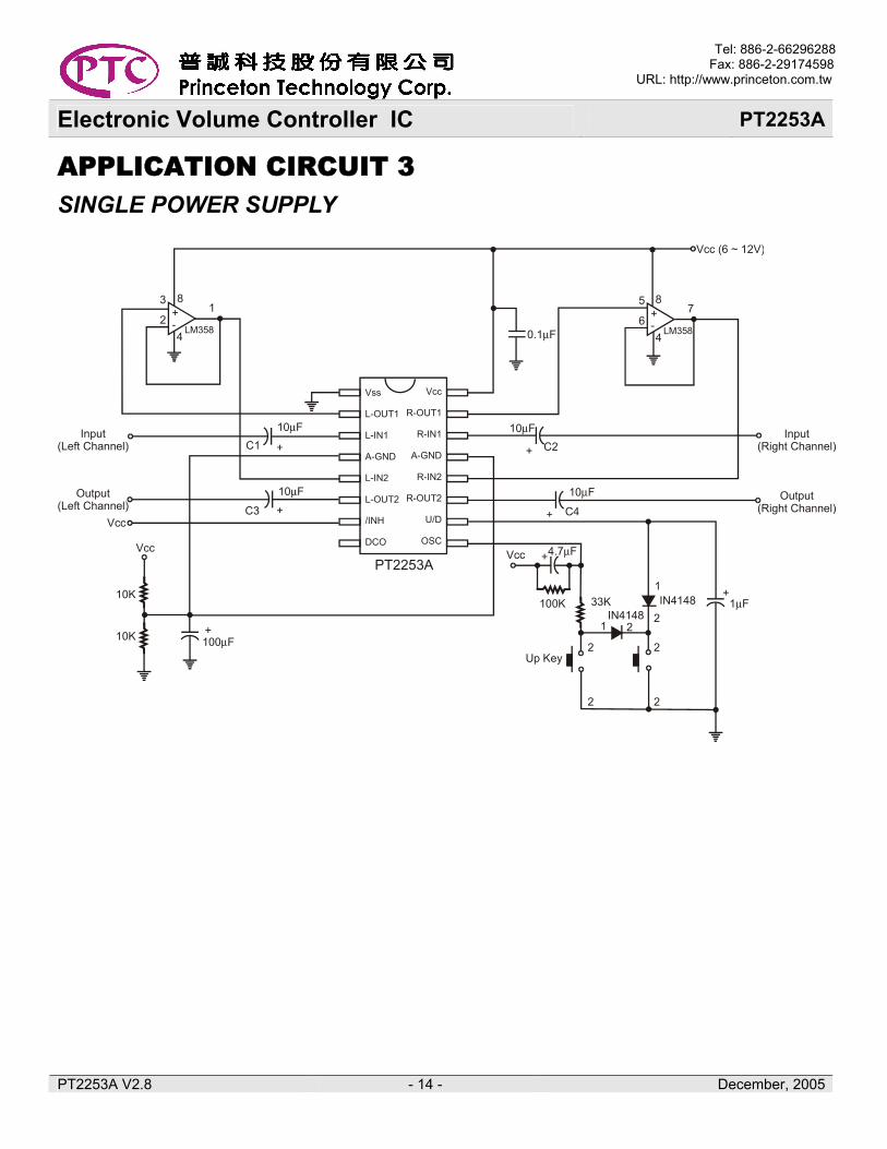
APPLICATION CIRCUIT 3 SINGLE POWER SUPPLY
10 Fµ 10 Fµ
10 Fµ 10 Fµ
+ +
+ +
Input (Left Channel) C1 C2
C3 C4Output
(Left Channel)Vcc
+100 Fµ
10K
10K
Vcc
Vcc (6 ~ 12V)
0.1 Fµ
Input(Right Channel)
Output(Right Channel)
1
2IN4148
IN414833K
22
22
1 2
1 Fµ+
Vcc +4.7 Fµ
100K
Up Key
- -+ +
4 42 6
3 51 7
LM358 LM358
8 8
Vss
L-OUT1
L-IN1
A-GND
L-IN2
L-OUT2
/INH
DCO
Vcc
R-OUT1
R-IN1
A-GND
R-IN2
R-OUT2
U/D
OSC
PT2253A
Tel: 886-2-66296288 Fax: 886-2-29174598 URL: http://www.princeton.com.tw
PT2253A V2.8 - 15 - December, 2005
Electronic Volume Controller IC PT2253A
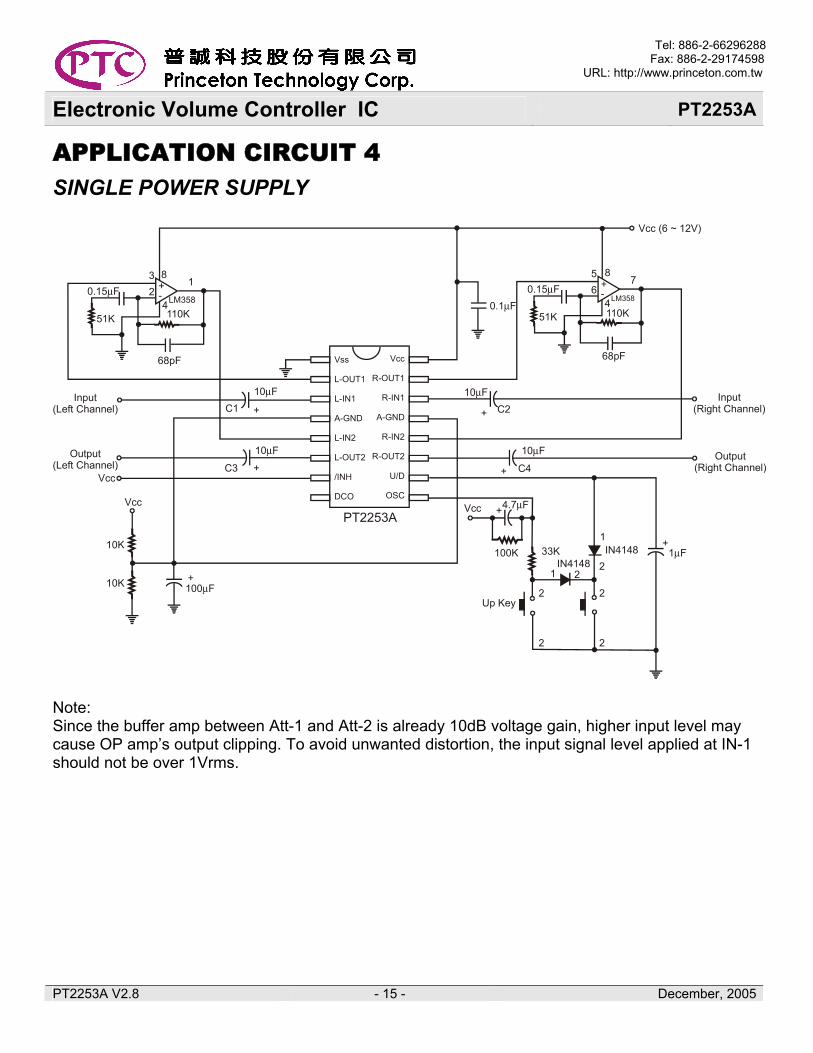
APPLICATION CIRCUIT 4 SINGLE POWER SUPPLY
-+
42 6
51 7
68pF
110KLM358
0.15 Fµ
51K
-+
4
3
68pF
110KLM358
0.15 Fµ
51K
8 8
10 Fµ 10 Fµ
10 Fµ 10 Fµ
+ +
+ +
Input (Left Channel) C1 C2
C3 C4Output
(Left Channel)Vcc
+100 Fµ
10K
10K
Vcc
Vcc (6 ~ 12V)
0.1 Fµ
Input(Right Channel)
Output(Right Channel)
1
2IN4148
IN414833K
22
22
1 2
1 Fµ+
Vcc +4.7 Fµ
100K
Up Key
Vss
L-OUT1
L-IN1
A-GND
L-IN2
L-OUT2
/INH
DCO
Vcc
R-OUT1
R-IN1
A-GND
R-IN2
R-OUT2
U/D
OSC
PT2253A
Note: Since the buffer amp between Att-1 and Att-2 is already 10dB voltage gain, higher input level may cause OP amp’s output clipping. To avoid unwanted distortion, the input signal level applied at IN-1 should not be over 1Vrms.
Tel: 886-2-66296288 Fax: 886-2-29174598 URL: http://www.princeton.com.tw
PT2253A V2.8 - 16 - December, 2005
Electronic Volume Controller IC PT2253A
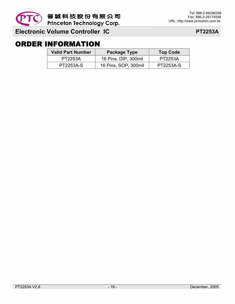
ORDER INFORMATION Valid Part Number Package Type Top Code
PT2253A 16 Pins, DIP, 300mil PT2253A PT2253A-S 16 Pins, SOP, 300mil PT2253A-S
Tel: 886-2-66296288 Fax: 886-2-29174598 URL: http://www.princeton.com.tw
PT2253A V2.8 - 17 - December, 2005
Electronic Volume Controller IC PT2253A
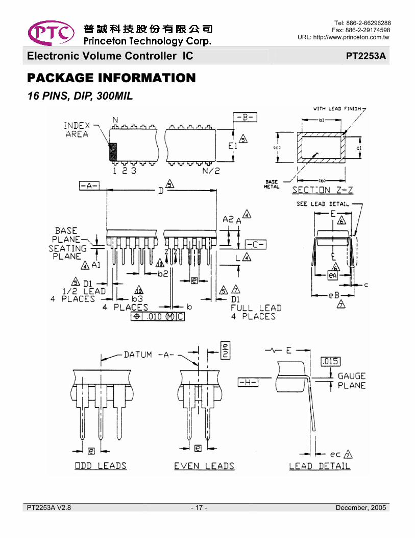
PACKAGE INFORMATION 16 PINS, DIP, 300MIL
Tel: 886-2-66296288 Fax: 886-2-29174598 URL: http://www.princeton.com.tw
PT2253A V2.8 - 18 - December, 2005
Electronic Volume Controller IC PT2253A
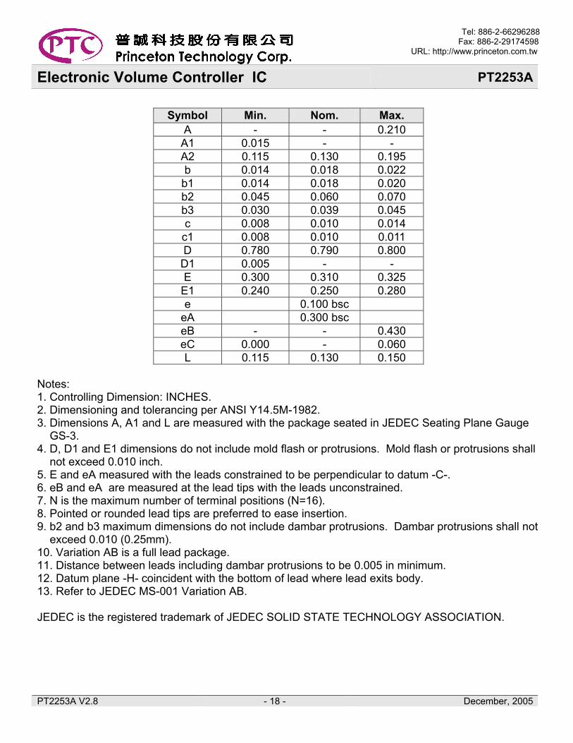
Symbol Min. Nom. Max.
A - - 0.210 A1 0.015 - - A2 0.115 0.130 0.195 b 0.014 0.018 0.022
b1 0.014 0.018 0.020 b2 0.045 0.060 0.070 b3 0.030 0.039 0.045 c 0.008 0.010 0.014 c1 0.008 0.010 0.011 D 0.780 0.790 0.800 D1 0.005 - - E 0.300 0.310 0.325
E1 0.240 0.250 0.280 e 0.100 bsc
eA 0.300 bsc eB - - 0.430 eC 0.000 - 0.060 L 0.115 0.130 0.150
Notes: 1. Controlling Dimension: INCHES. 2. Dimensioning and tolerancing per ANSI Y14.5M-1982. 3. Dimensions A, A1 and L are measured with the package seated in JEDEC Seating Plane Gauge GS-3. 4. D, D1 and E1 dimensions do not include mold flash or protrusions. Mold flash or protrusions shall not exceed 0.010 inch. 5. E and eA measured with the leads constrained to be perpendicular to datum -C-. 6. eB and eA are measured at the lead tips with the leads unconstrained. 7. N is the maximum number of terminal positions (N=16). 8. Pointed or rounded lead tips are preferred to ease insertion. 9. b2 and b3 maximum dimensions do not include dambar protrusions. Dambar protrusions shall not exceed 0.010 (0.25mm). 10. Variation AB is a full lead package. 11. Distance between leads including dambar protrusions to be 0.005 in minimum. 12. Datum plane -H- coincident with the bottom of lead where lead exits body. 13. Refer to JEDEC MS-001 Variation AB. JEDEC is the registered trademark of JEDEC SOLID STATE TECHNOLOGY ASSOCIATION.
Tel: 886-2-66296288 Fax: 886-2-29174598 URL: http://www.princeton.com.tw
PT2253A V2.8 - 19 - December, 2005
Electronic Volume Controller IC PT2253A
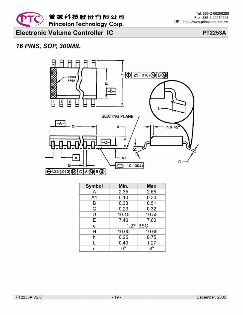
16 PINS, SOP, 300MIL
Symbol Min. Max A 2.35 2.65
A1 0.10 0.30 B 0.33 0.51 C 0.23 0.32 D 10.10 10.50 E 7.40 7.60 e 1.27 BSC H 10.00 10.65 h 0.25 0.75 L 0.40 1.27 α 0o 8o
Tel: 886-2-66296288 Fax: 886-2-29174598 URL: http://www.princeton.com.tw
PT2253A V2.8 - 20 - December, 2005
Electronic Volume Controller IC PT2253A
Notes: 1. Controlling Dimension: MILLIMETER 2. Dimensioning and tolerancing per ANSI Y14.5M-1982. 3. Dimension D does not include mold flash, protrusions or gate burrs. Mold flash, protrusions and gate burrs shall not exceed 0.15mm (0.006 in) per side. 4. Dimension E does not include interlead flash or protrusions. Interlead flash and protrusions shall not exceed 0.25 mm (0.010 in.) per side. 5. The chamfer on the body is optional. If it is not present, a visual index feature must be located within the crosshatched area. 6. L is the length of the terminal for soldering to a substrate. 7. N is the number of terminal positions (N=16). 8. The lead width B, as measured 0.36 mm (0.014in) or greater above the seating plane, shall not exceed a maximum value of 0.61mm (0.024in.) 9. Refer to JEDEC MS-013 Variation AA. JEDEC is the registered trademark of JEDEC SOLID STATE TECHNOLOGY ASSOCIATION.