Dependence on Feature Size - University of...
25
Dependence on Feature Size Gary Drake Argonne National Laboratory University of Chicago Workshop Apr. 29, 2011 The Factors That Limit Time Resolution in Photodetectors
Transcript of Dependence on Feature Size - University of...

Dependence on Feature Size
Gary DrakeArgonne National Laboratory
University of Chicago WorkshopApr. 29, 2011
The Factors That Limit Time Resolution in Photodetectors

Outline Basic Notation
Survey of Feature Sizes
How Feature Size Affects Speed – Scaling Laws
Consequences of Deep Submicron Technologies
Practical Considerations
Summary
2

Basic Notations & Principles in CMOS Design Geometry
W = Gate Width L = Gate Length tox = thickness of gate oxide W/L – defines transistor size Lmin = min. feature size
Semiconductor Construction N-type – mobile charge carriers
are electrons (negative charge) P-type – mobile charge carriers
are holes (positive charge) Doping – add impurities to pure silicon
to make material N-type or P-type ♦ Na – density of acceptor atoms - holes♦ Nd – density of donor atoms - electrons
NMOS or N-channel - electrons♦ Conductive channel is N-type
PMOS or P-channel - holes♦ Conductive channel is P-type
Source & Drain – doping implants into substrate to create n+ & p+ regions
Oxide Layer - Gate is isolated from substrate, which makes it high impedance, except for leakage
Operation Gate-Source voltage VGS creates
conduction channel under gate, allowing current to flow between drain & source
Minimum gate voltage to create channel called the Threshold Voltage VTH
P-
substratechannel
source
gate
drain
toxoxide W
L
Modified Graphic Courtesy of Kaushik Roy, Purdue
Construction of NMOS FET
3

Survey of Feature Sizesor
Size DOES Matter!
Big is Good!
Big is Good!
Big is Good!
Big is Good?Small is Good.
But not too small…
Big is Good?
4

Technologies - IBM & TSMC CMOS
0 100 200 300 400 500 600
Size (nm)
Survey of Feature SizesIBM & TSMC CMOS ProcessesOffered Through MOSIS Today
45 nm65 nm90 nm
0.130 m0.180 m
0.250 m
0.350 m
0.500 m
Trusted Vendor
OnlyAvailable Thru MOSIS Being Discontinued
32 nm28 nm
22 nm
TSMCOnly
Data from MOSIS
40 nm
5

The Basic Question:How to Achieve Faster (Higher BW) ASICS?
The Basic Answer: General trend:
The smaller the feature size, the faster the chip can operate. Why? A few high-level reasons:
♦ Smaller size = shorter distance that signals need to propagate♦ Smaller size = generally lower parasitic capacitance
(But watch out for larger capacitance/unit area…)♦ Smaller size use lower voltage rails reach logic levels faster
More technical answers later…
d1
d2
C1
C2
Shorter transmission distance Smaller capacitances Lower voltage rails6

IBM CMOS Process - Ring Oscillator Frequency (MHz) by Technology
0
100
200
300
400
500
600
700
800
Rin
g O
scill
ator
Fre
q (M
Hz)
The Basic Question:How to Achieve Faster (Higher BW) ASICS? (Cont.)
Measurements Tell the Tale: One measure of speed in CMOS: Ring Oscillator Frequency
♦ Basic test structure used by MOSIS to measure fabrication run acceptance♦ Generally configured as an odd number of inverters, minimum-sized devices
F0 = 1/(2N * Inverter_delay), N = # Inverters (MOSIS uses 31 stages.)
Data from MOSIS
Courtesy Wikipedia
Smaller Feature Size
22 n
m
28 n
m
32 n
m
45 n
m
65 n
m
65 n
m
90 n
m
90 n
m
0.13
0 m
0.13
0 m
0.18
0 m
0.18
0 m
0.18
0 m
0.25
0 m
0.35
0 m
0.50
0 m
0.18
0 m
(Line Not a Fit…)
7

How Feature Size Affects Speed Robert Dennard’s Scaling Law (1974)
If scale the physical parameters of an integrated circuit equally by factor K, then performance parameters scale as follows:
Slide Courtesy of Hiiroshi Iwai, Tokyo Institute of Technology
Table Courtesy of Mark Bohr, IBM
K1/KKKKKK2
1
8

How Feature Size Affects Speed (Cont.) Dennard’s Scaling Law & Moore’s Law
Gordon Moore’s Law: “The number of transistors that can placed inexpensively on an integrated circuit doubles approximately every two years.” Basis for Industry Roadmap (ITRS)
Dennard: If scale physical dimensions by K, then area of chip ~ K2
♦ For K ~0.7 ~ 1/SQRT(2), K2 ~ ½ X2 more transistors for a given die size Industry: Ratios between successive technology steps:
350/500 = 0.7; 250/350 = 0.71; 90/130 = 0.69; 65/90 = 0.722
Plots Courtesy of Mark Bohr, IBM
Inte
l Pro
cess
ors
Year YearMoore’s Law will come to an end in ~2014, when the feature size approaches a few atomic layers. 9

How Feature Size Affects Speed (Cont.) Examining Speed versus Technology
A technical answer from semiconductor physics (Courtesy of Willy Sansen):
Critical Parameters:• Mobility • Channel Length• Thresh. Voltage• VGS-VT
These are functions of the technology…
(fT = Freq. where current gain = 1)
10

How Feature Size Affects Speed (Cont.) Examining Speed versus Technology (Cont.)
Unity Gain Frequency:
Length L
Carrier Mobility
VT & (VGS – VT) ?♦ Want (VGS – VT) as large as possible♦ Want VT as small as possible
Critical Parameters:• Mobility • Channel Length• Thresh. Voltage• VGS-VT
ND 1/K Increases for K<1
Decreases as feature size decreases, L K scaling, for K < 1 Causes fT to increase as 1/K2 for K < 1
fT decreases for K<1, but slowly…
11

How Feature Size Affects Speed (Cont.) Examining Speed versus Technology (Cont.)
Generally, threshold voltage VTH
gets smaller with feature size♦ Partly a consequence of decreasing Vdd
♦ Partly a consequence of increasing COX (aF/m2 gate area)
But, are approaching a limit with submicron technologies… Why?
where Vfb is the flatband voltage, vT = kT/qCOX is the gate oxide capacitance/areaB is the zero bias mobilityVbs is the max. depletion layer widthNa is the acceptor doping density
IBM CMOS Process - N-Channel Minimum Threshold Voltage by Technology
0
0.1
0.2
0.3
0.4
0.5
0.6
0.7
Thre
shol
d Vo
ltage
(Vol
ts)
22 n
m
28 n
m
32 n
m
45 n
m
65 n
m
65 n
m
90 n
m
90 n
m
0.13
0 m
0.13
0 m
0.18
0 m
0.18
0 m
0.18
0 m
0.25
0 m
0.35
0 m
0.50
0 m
0.18
0 m
Data from MOSIS
(Line Not a Fit…)
12
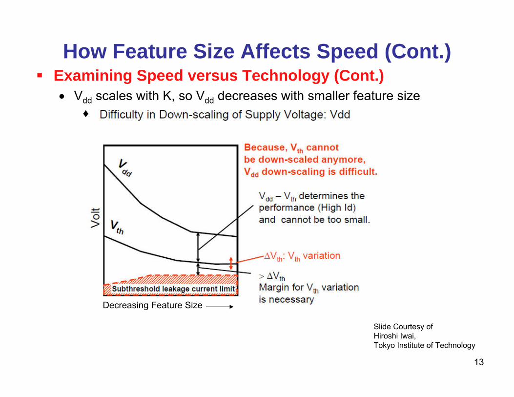
How Feature Size Affects Speed (Cont.)
Slide Courtesy ofHiroshi Iwai, Tokyo Institute of Technology
Examining Speed versus Technology (Cont.) Vdd scales with K, so Vdd decreases with smaller feature size
♦
Decreasing Feature Size
13

How Feature Size Affects Speed (Cont.) Examining Speed versus Technology (Cont.)
Bottom Line - Unity Gain Frequency of FETs:
Approaching a constant
Scales with K
Decreases as (K)0.7
So, fT 1/K (approximate) i.e., fT increases as feature size decreases
14

Consequences of Deep Submicron Technologies Scaling Laws worked well until ~ 100 nm and smaller
Performance generally well-predicted > 100 nm Below 100 nm, start to see second-order and higher-order
effects that affect performance♦ Especially for analog IC or mixed-signal ICs
Direct Performance Effects Increased leakage currents
♦ Increased power consumption Transistor size mismatch
Other Performance Factors Especially for Analog Reduced voltage rails Decreased signal-to-noise Decreased dynamic range Increased power density
Graphic Courtesy of Kaushik Roy, Purdue University
15

Consequences of Deep Submicron Technologies (Continued)
Leakage Currents Gate oxide tunneling leakage (IG)
♦ Thin gate oxides allow electron tunneling from gate to substrate
♦ Major source of leakage current in sub-micron CMOS
♦ The thinner the oxide, the worse the leakage current, i.e. the smaller the feature size, the worse the leakage current, since tox scales
Plot Courtesy of Kaushik Roy, Purdue University
IBM CMOS Process - Oxide Thickness by Technology
0
10
20
30
40
50
60
70
Oxi
de T
hick
ness
(Ang
stro
ms)
Data from MOSIS
Gate Oxide tox
Graphic Courtesy of Kaushik Roy, PurdueON & OFF States
22 n
m
28 n
m
32 n
m
45 n
m
65 n
m
65 n
m
90 n
m
90 n
m
0.13
0 m
0.13
0 m
0.18
0 m
0.18
0 m
0.18
0 m
0.25
0 m
0.35
0 m
0.50
0 m
0.18
0 m
Simulation
(Line Not a Fit…)
16

Consequences of Deep Submicron Technologies (Continued)
where Vth is the threshold voltage, vT = kT/qCOX is the gate oxide capacitanceOX is the zero bias mobilityWdm is the max. depletion layer width Graphics Courtesy of Kaushik Roy, Purdue University
Modified Graphic Courtesy of Kaushik Roy, Purdue
Leakage Currents (Cont.) Subthreshold leakage (ISUB)
♦ Drain-source current during weak inversion, VGS < VTH
♦ Dominated by diffusion current of minority carriers, rather than drift current that dominates in strong inversion
♦ Carriers move along surface♦ Very sensitive to process parameters,
device size, supply voltage, and temperature
VDS dominates at Drain-substratejunction
Minority carrier ConcentrationIn channel
Subthreshold LeakageLog(ID) vs. VGS
OFF State
Magnitude increases as feature size decreases
17

Consequences of Deep Submicron Technologies (Continued)
Graphics Courtesy of Kaushik Roy, Purdue University
Modified Graphic Courtesy of Kaushik Roy, Purdue
ON & OFF States
Leakage Currents (Cont.) PN Junction Reverse-Bias Leakage (IREV)
♦ 2 mechanisms– Minority-carrier drift/diffusion– Electron-hole generation
♦ Occurs when P & N junctions are heavily doped
– Doping (Na & Nd) increases as feature size decreases Leakage increases as feature size decreases
– Causes band-to-band tunneling (BTBT) due to electric field from the doping
18

Consequences of Deep Submicron Technologies (Continued)
Graphics Courtesy of Kaushik Roy, Purdue University
Modified Graphic Courtesy of Kaushik Roy, Purdue
OFF State
Leakage Currents (Cont.) Gate Induced Drain Leakage (IGIDL)
♦ Caused by narrowing of depletion region around drain when FET is off
– Due to electric field between gate and drain
♦ Get tunneling of minority carriers from drain to substrate
♦ Strong function of – Doping profile at drain edge– Oxide thickness– Vdd
Surface is accumulatedwith low negative gate bias
Surface is depletedwith high negative gate bias,allowing tunneling ofminority carriers into substrate 19

Consequences of Deep Submicron Technologies (Continued)
Matching Problems Generally, device matching becomes worse as feature size
decreases♦ Limitations of lithography & processing
Slope is gentle … Many designs may not be affected …
Plot Courtesy ofHiroshi Iwai, Tokyo Institute of TechnologyPlot Courtesy of
Willy Sansen
20

Other Consequences of Deep Submicron Technologies Reduced Headroom
Circuits with more than ~2-3 transistors between Vdd and Vss run out of head room due to reduced Vdd (scales with K…)
Reduced Signal-to-Noise Reduced voltage rails mean smaller signals Noise may not improve with smaller feature size
♦ Depends on design…
Reduced Dynamic Range Also a consequence of reduced voltage rails and higher noise…
Increased Power Density Consequence of leakage currents
For digital, these are mostly OK For analog, can be a problem…
21
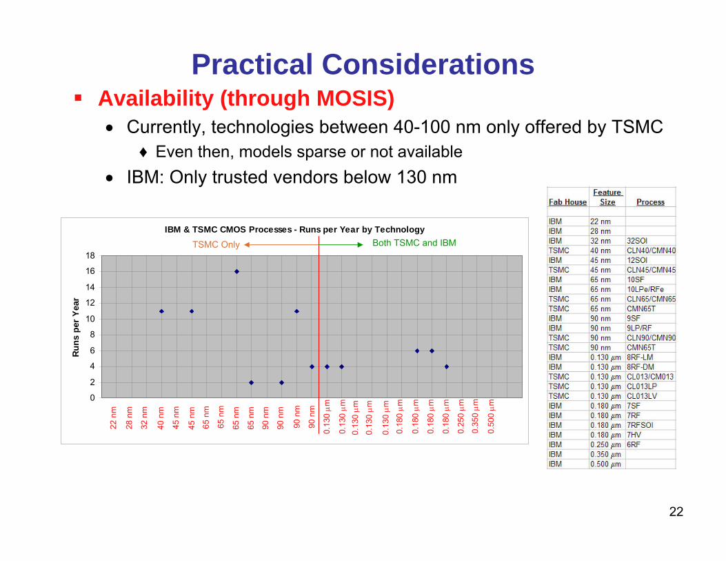
IBM & TSMC CMOS Processes - Runs per Year by Technology
0
2
4
6
8
10
12
14
16
18
Runs
per
Yea
rPractical Considerations
Availability (through MOSIS) Currently, technologies between 40-100 nm only offered by TSMC
♦ Even then, models sparse or not available IBM: Only trusted vendors below 130 nm
22 n
m
28 n
m
32 n
m
45 n
m
65 n
m
65 n
m
90 n
m
90 n
m
0.13
0 m
0.13
0 m
0.18
0 m
0.18
0 m
0.18
0 m
0.25
0 m
0.35
0 m
0.50
0 m
0.18
0 m
40 n
m
45 n
m
65 n
m
65 n
m
90 n
m
90 n
m
0.13
0 m
0.13
0 m
0.13
0 m
TSMC Only Both TSMC and IBM
22

Practical Considerations Cost
(Costs unknown for every technology at press time…) Generally, leading-edge technologies very expensive,
even through MOSIS
Models Models are poor – to – non-existent for leading-edge technologies Customer support is poor for leading-edge technologies MOSIS data not available for leading-edge technologies
General Difficulty Expect long learning curve with the more advanced technologies
23

Summary For high-speed and high-bandwidth,
generally want technologies with smaller feature size Smaller distances Smaller parasitic capacitances Smaller voltage swings Intrinsically faster devices (from scaling law principles)
Below ~ 100 nm, start to have higher-order problems Leakage currents of various kinds can affect designs
♦ Higher internal power♦ May significantly affect analog circuits, in particular sample & hold circuits
Matching of transistors is worse Signal headroom is reduced Dynamic range is reduced
Prospects for near future Scaling laws have worked beautifully for 40 years, but we’re reaching a hard limit Industry has kept pace, but will have difficulty below 10 nm Leading-edge technologies difficult to use right now, but this will improve Not clear if higher-order process problems can be solved for analog use… Perhaps clever circuit design can be employed, but this will take time…
130 nm technology is not a bad place to be right now for analog work…24

Bibliography
ROY, K., MUKHOPADHYAY, S., MAHMOODI-MEIMAND, S., “Leakage Current Mechanisms and LeakageReduction Techniques in Deep-Submicrometer CMOS Circuits,” PROCEEDINGS OF THE IEEE, VOL. 91, NO. 2, FEBRUARY 2003, pp. 305-327
Sansen., W., “Analog IC Design in Nanometer CMOS Technologies,” Presentation, New Delhi, Jan., 2009.
IEEE SSCS NEWSLETTER, Winter, 2007.
Iwai, H., “Technology Roadmap for 22nm CMOS and Beyond,” Presentation, IEDST 2009, Bombay, June 1, 2009.
25