DEPARTMENT OF ELECTRICAL ENGINEERING LABORATORY …mjcollege.ac.in/images/labmannuals/III EEE II SEM...
66
DEPARTMENT OF ELECTRICAL ENGINEERING LABORATORY MANUAL INTEGRATED CIRCUITS LAB (EE 383) For III/IV B.E I /II SEM EIE & EEE DEPARTMENT OF ELECTRICAL ENGINEERING MUFFAKHAM JAH COLLEGE OF ENGINEERING & TECHNOLOGY Banjara Hills Road No 3, Hyderabad 34 www.mjcollege.ac.in
Transcript of DEPARTMENT OF ELECTRICAL ENGINEERING LABORATORY …mjcollege.ac.in/images/labmannuals/III EEE II SEM...

DEPARTMENT OF ELECTRICAL ENGINEERING
LABORATORY MANUAL
INTEGRATED CIRCUITS LAB (EE 383)
For
III/IV B.E I /II SEM EIE & EEE
DEPARTMENT OF ELECTRICAL ENGINEERINGMUFFAKHAM JAH COLLEGE OF ENGINEERING & TECHNOLOGY
Banjara Hills Road No 3, Hyderabad 34www.mjcollege.ac.in
MUFFAKHAM JAH COLLEGE OF ENGINEERING & TECHNOLOGY
INTEGRATED CIRCUITS LAB
List Of Experiments Page no
1. Active Filters Using Op Amps 01
2. Astable Multivibrator Using 555 Timer IC 11
3. Multiplexer - Logic Realization Of Combinational Circuits 15
4. Triangular, Square & Sine wave generator 18
5. Adders & Subtractors realization of combinational Logic 24
6. Clippers & Clampers using Op amps 28
7. Design of Integrator & Differentiator Using OP Amp 34
8. Phase Locked Loop 41
9. Synchronous Counter 46
10. Asynchronous counter 50
11. D/A Converter 54
12. A/D Converter 57
13. Monostable Multivibrator Using IC 555 60

Experiment no:1
ACTIVE FILTERS
AIM: 1.To Design and study the active filters of low pass, high pass, band pass,band reject using op-amps.
2. Calculate the practical filter frequencies and plot the frequency response foreach Filter
EQUIPMENTS & COMPONENTS: 1.Active Filters kit2. 30MHz C.R.O.3. Multimeter4. Connecting patch chords.5. Signal generator
THEORY:
FILTER DESIGN OF FIRST ORDER LOW PASS FILTER:
Gain of the filter =Vin
VO
A = 1 +1R
R F(Pass band gain)
Higher cut – off frequency (fh) =RC21
1. Choose a value of high cut – off frequency fH.2. Select the C (which is provided on the trainer).3. Calculate the R value
R =CfH2
1Adjust the pot resistance equal to the R-value
FILTER DESIGN OF FIRST ORDER LOW PASS FILTER:
Gain of the filter =Vin
VO
Integrated Circuits Lab, MJCET EED
2
AF = 1 +1R
R F(Pass band gain)
Lower cut – off frequency (fL) =RC21
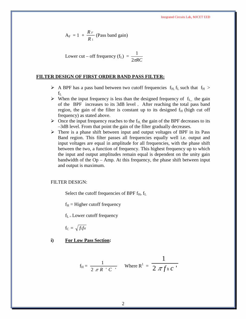
FILTER DESIGN OF FIRST ORDER BAND PASS FILTER:
A BPF has a pass band between two cutoff frequencies fH, fL such that fH >fL
When the input frequency is less than the designed frequency of fL,. the gainof the BPF increases to its 3dB level . After reaching the total pass bandregion, the gain of the filter is constant up to its designed fH (high cut offfrequency) as stated above.
Once the input frequency reaches to the fH, the gain of the BPF decreases to its–3dB level. From that point the gain of the filter gradually decreases.
There is a phase shift between input and output voltages of BPF in its PassBand region. This filter passes all frequencies equally well i.e. output andinput voltages are equal in amplitude for all frequencies, with the phase shiftbetween the two, a function of frequency. This highest frequency up to whichthe input and output amplitudes remain equal is dependent on the unity gainbandwidth of the Op – Amp. At this frequency, the phase shift between inputand output is maximum.
FILTER DESIGN:
Select the cutoff frequencies of BPF fH, fL
fH = Higher cutoff frequency
fL = Lower cutoff frequency
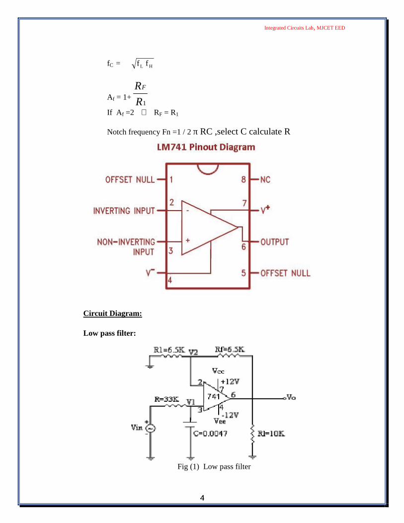
fC = HLff
i) For Low Pass Section:
fH =''2
1
CRWhere R1 = '2
1
cf h

Integrated Circuits Lab, MJCET EED
3
ii) For high pass section:
fL =RC21
Where R =Cf L2
1
If the band pass gain is 4 the gain of the high pass as well as low passsection could be set to 2 i.e. input and feedback resistors must be equal invalue. The magnitude of voltage gain is given by
i
O
V
V=
1/22H
2L ))(f/f(1))(f/f(1
)/(
++LFT ffA
Where AFT = Total Pass band gain
f = Signal input frequency (Hz)
fL = Low cutoff frequency
fH = High Cutoff frequency
fC = HLff
DESIGN OF FIRST ORDER BAND REJECT or NOTCH FILTER:
A BRF has a stop band between the cutoff frequency fH&fL such tha fH < fL.
When the input frequency is less than the designed frequency of fH ,the gain ofthe BRF is constant up to fH . In other words it allows the frequencies equallywell that is output and input voltages are equal in amplitude.
By increasing the input frequency after fH , the gain gradually decreases to itscenter frequency fC . After this increases to its 3db level. After reaching thetotal pass band region. The gain of the filter is again constant up to itsdesigned fH (High cutoff frequency) as stated above.
FILTER DESIGN:
Select the cut off frequency of BRF fH, fL
fH = Higher cutoff frequencyfL = Lower cutoff frequency
Integrated Circuits Lab, MJCET EED
4
fC = HL ff
Af = 1+1R
RF
If Af =2 ⇒ RF = R1
Notch frequency Fn =1 / 2 π RC ,select C calculate R
Circuit Diagram:
Low pass filter:
Fig (1) Low pass filter
Integrated Circuits Lab, MJCET EED
4
fC = HL ff
Af = 1+1R
RF
If Af =2 ⇒ RF = R1
Notch frequency Fn =1 / 2 π RC ,select C calculate R
Circuit Diagram:
Low pass filter:
Fig (1) Low pass filter
Integrated Circuits Lab, MJCET EED
4
fC = HL ff
Af = 1+1R
RF
If Af =2 ⇒ RF = R1
Notch frequency Fn =1 / 2 π RC ,select C calculate R
Circuit Diagram:
Low pass filter:
Fig (1) Low pass filter

Integrated Circuits Lab, MJCET EED
5
Lpf fh=10 kHz TO 11 kHz
Hpf fl=11 kHz
B.P.F B.W =1 kHz to 4 kHz(1 kHz to 1.75 kHz)
B.R.F fh=1.5 kHzC = 0.1 µf,R= 9.1 K ohms
Fig (2) Frequency response
PROCEDURE:
1. Connect the circuit as shown in figure1.using filter kit
2. Choose the R1 and Rf values depending on the pass band gain of the filter Af
Af=1+(Rf/R1) choose 6.5 K for high Rf and R1 then pass band gain=2
3. Choose a value for high cut off frequency f H
4. Calculate the R using R=1/2ΠfH C where C=0.0047µF.
5. Connect the function generator to the input of the filter of fixed amplitude.of 2V PP For different values of input signal frequency F. Note the correspondingoutput voltage.
6. Calculate pass band gain Af which is given by Af=Vo/Vin for differentfrequencies, note down in the tabular column, record and observe the gain ofthe filter
Integrated Circuits Lab, MJCET EED
6
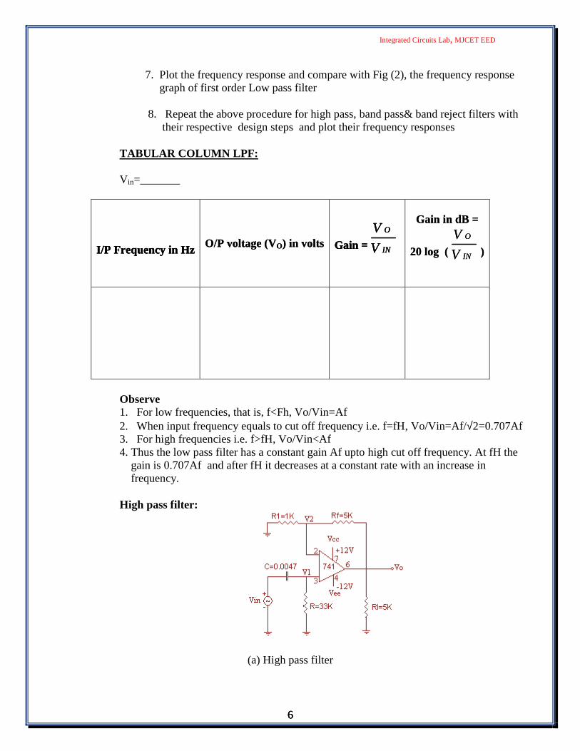
7. Plot the frequency response and compare with Fig (2), the frequency responsegraph of first order Low pass filter
8. Repeat the above procedure for high pass, band pass& band reject filters withtheir respective design steps and plot their frequency responses
TABULAR COLUMN LPF:
Vin=_______
I/P Frequency in Hz O/P voltage (VO) in volts Gain = IN
O
V
VGain in dB =
20 log ( IN
O
V
V)
Observe1. For low frequencies, that is, f<Fh, Vo/Vin=Af2. When input frequency equals to cut off frequency i.e. f=fH, Vo/Vin=Af/√2=0.707Af3. For high frequencies i.e. f>fH, Vo/Vin<Af4. Thus the low pass filter has a constant gain Af upto high cut off frequency. At fH the
gain is 0.707Af and after fH it decreases at a constant rate with an increase infrequency.
High pass filter:
(a) High pass filter
Integrated Circuits Lab, MJCET EED
6
7. Plot the frequency response and compare with Fig (2), the frequency responsegraph of first order Low pass filter
8. Repeat the above procedure for high pass, band pass& band reject filters withtheir respective design steps and plot their frequency responses
TABULAR COLUMN LPF:
Vin=_______
I/P Frequency in Hz O/P voltage (VO) in volts Gain = IN
O
V
VGain in dB =
20 log ( IN
O
V
V)
Observe1. For low frequencies, that is, f<Fh, Vo/Vin=Af2. When input frequency equals to cut off frequency i.e. f=fH, Vo/Vin=Af/√2=0.707Af3. For high frequencies i.e. f>fH, Vo/Vin<Af4. Thus the low pass filter has a constant gain Af upto high cut off frequency. At fH the
gain is 0.707Af and after fH it decreases at a constant rate with an increase infrequency.
High pass filter:
(a) High pass filter

Integrated Circuits Lab, MJCET EED
7
(b) Frequency response
TABULAR COLUMN HPF:
Vin=_______
I/P Frequency in Hz O/P voltage (VO) in volts Gain = IN
O
V
VGain in dB =
20 log ( IN
O
V
V)
Observe1. For low frequencies, that is, f<fL, Vo/Vin<Af2. When input frequency equals to cut off frequency i.e. f=fL
Vo/Vin=Af/√2=0.707Af3. For high frequencies i.e. f>fL, Vo/Vin=Af4. Thus the high pass filter has a constant gain Af from low cut off frequency to
Higher cut off frequencies. At fL the gain is 0.707Af below fL it decreases at aConstant rate with an decrease in frequency.
Integrated Circuits Lab, MJCET EED
8
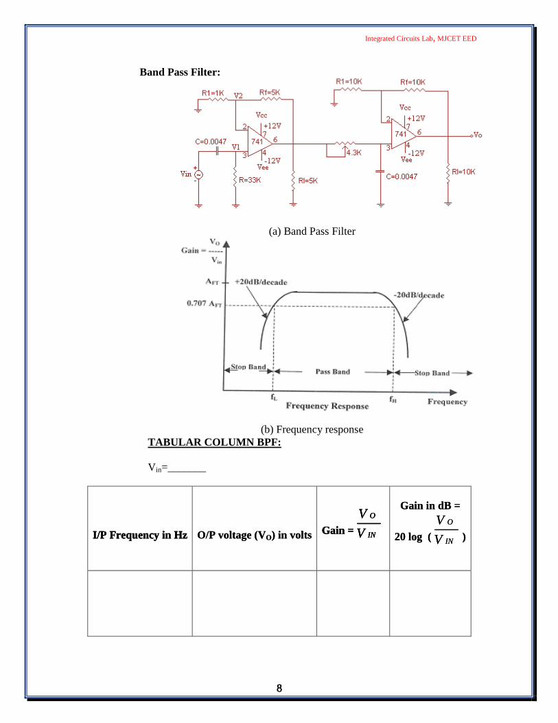
Band Pass Filter:
(a) Band Pass Filter
(b) Frequency responseTABULAR COLUMN BPF:
Vin=_______
I/P Frequency in Hz O/P voltage (VO) in volts Gain = IN
O
V
VGain in dB =
20 log ( IN
O
V
V)
Integrated Circuits Lab, MJCET EED
8
Band Pass Filter:
(a) Band Pass Filter
(b) Frequency responseTABULAR COLUMN BPF:
Vin=_______
I/P Frequency in Hz O/P voltage (VO) in volts Gain = IN
O
V
VGain in dB =
20 log ( IN
O
V
V)
Integrated Circuits Lab, MJCET EED
8
Band Pass Filter:
(a) Band Pass Filter
(b) Frequency responseTABULAR COLUMN BPF:
Vin=_______
I/P Frequency in Hz O/P voltage (VO) in volts Gain = IN
O
V
VGain in dB =
20 log ( IN
O
V
V)

Integrated Circuits Lab, MJCET EED
9
Observe1. For frequencies lower than fL and higher than fH ,Vo/Vin < Af2. When input frequency equals to cut off frequency i.e. f = fH = fL
Vo/Vin = Af/√2 = 0.707Af3.For frequencies ranging from fL to fH, Vo/Vin = Af
Band Reject Filter:
(a) Band Reject Filter
(b) Frequency response
fN=1/2πRCC=0.007µF,R=33K,R1=R2=33K ohmfN=4.8kHz

Integrated Circuits Lab, MJCET EED
10
TABULAR COLUMN BRF:
Vin=_______
I/P Frequency in Hz O/P voltage (VO) in volts Gain = IN
O
V
VGain in dB =
20 log ( IN
O
V
V)
Observe
1. For frequencies lower than fL and higher than fH ,Vo/Vin < Af2.When input frequency equals to cut off frequency i.e. f = fH = fL
Vo/Vin = Af/√2 = 0.707Af3. For frequencies ranging from fL to fH,Vo/Vin = Af
4.When input frequency equals to cut off frequency i.e. f = foVo/Vin<Af And frequencies other than fo, Vo/Vin = Af
DISCUSSION OF RESULT:
1. Students will observe the frequency responses of various filters and discuss the applicationsrelated and will be able to comment on filter specifications.2. Various regional bands of filters can be observed and selected for specific filters
PRELAB QUESTIONS:
1. What are the applications of filters?2. What is difference between Active and Passive filters?3. What are the advantages & disadvantages of Active filters?4. What happens to filter response as the order of filter increases?5. Where is all pass filter applicable?6. What is transition band of a filter?7. Define Q factor of a filter. how is it related to Corner frequency Fc?

Integrated Circuits Lab, MJCET EED
11
Experiment no:2
ASTABLE MULTIVIBRATOR
AIM: 1.To study and design IC 555 timer as an Astable multivibrator.2. Calculate the frequency of oscillations & time period of output Waveform.
EQUIPMENTS : 1.IC Trainer kit./ Bread Board2.20MHz C.R.O.3.Multimeter4.Connecting patch chords.5.variable R.P.S
COMPONENTS: 1. IC 555 Timer2. Resistors 10 K , 4.7K
3. Capacitors 0.1µF(104), 0.01µF(103)4. Single stand wires
INTRODUCTION:
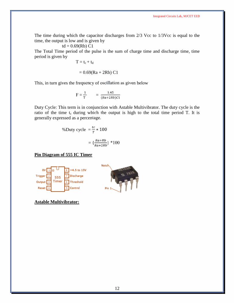
The 555 Timer is used in number of applications; it can be used as monostable,astable multivibrators, DC to DC converters, digital logic probes, analogy frequencyvoltage regulators and time delay circuits.The IC 555 timer is 8-pin IC and it can operate in free- running (Astable Multivibrator)mode or in one-shot (Monostable Multivibrator) mode. Pin configuration is as shown fig(1.). It can produce accurate and highly stable time delays or oscillations.
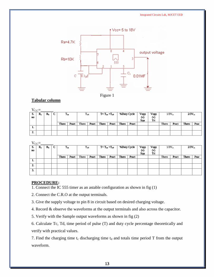
THEORY:
Astable Multivibrator often called a free-running Multivibrator. External Trigger input isnot required to operate the 555 as an Astable Configuration. However, the time duringwhich the output is either high or low is determined by two external components Resistor& Capacitor.Fig (1) shows the 555 as Astable Multivibrator. Initially, when the output is high,capacitor C starts charging towards Vcc through resistor Ra and Rb. As soon as voltageacross the capacitor equals to 2/3 Vcc, comparator-1 triggers the flip-flop, and the outputis low. Now capacitor discharges through Rb and transistor Q1. When the voltage acrosscapacitor c equals to 1/3Vcc, comparator-2’s output triggers the flip-flop, and the outputgoes high. Then the cycle repeats. The output voltage waveforms are as shown in fig (2).In this way capacitor periodically charges discharges between 2/3Vcc and 1/3Vccrespectively.The time during which the capacitor charges from 1/3Vcc to 2/3 Vcc is equal to the time,the output is high and is given by
tc = 0.69(Ra + Rb) C1
Integrated Circuits Lab, MJCET EED
12
The time during which the capacitor discharges from 2/3 Vcc to 1/3Vcc is equal to thetime, the output is low and is given by
td = 0.69(Rb) C1The Total Time period of the pulse is the sum of charge time and discharge time, timeperiod is given by
T = tc + td
= 0.69(Ra + 2Rb) C1
This, in turn gives the frequency of oscillation as given below
F = =.( )
Duty Cycle: This term is in conjunction with Astable Multivibrator. The duty cycle is theratio of the time tc during which the output is high to the total time period T. It isgenerally expressed as a percentage.
%Duty cycle = ∗ 100= *100
Pin Diagram of 555 IC Timer
Astable Multivibrator:
Integrated Circuits Lab, MJCET EED
13
Figure 1Tabular column
VCC=______S.no
Ra Rb C Ton Toff T= Ton +Toff %Duty Cycle Vopp(v)Squ
Vopp(v)Tri
1/3Vcc 2/3Vcc
Thero Pract Thero Pract Thero Pract Thero Pract Thero Pract Thero Prac1.
2.
VCC=______S.no
Ra Rb C Ton Toff T= Ton +Toff %Duty Cycle Vopp(v)Squ
Vopp(v)Tri
1/3Vcc 2/3Vcc
Thero Pract Thero Pract Thero Pract Thero Pract Thero Pract Thero Prac1.
2.
3.
PROCEDURE:1. Connect the IC 555 timer as an astable configuration as shown in fig (1)
2. Connect the C.R.O at the output terminals.
3. Give the supply voltage to pin 8 in circuit based on desired charging voltage.
4. Record & observe the waveforms at the output terminals and also across the capacitor.
5. Verify with the Sample output waveforms as shown in fig (2)
6. Calculate Tc, Td, time period of pulse (T) and duty cycle percentage theoretically and
verify with practical values.
7. Find the charging time tc discharging time td and totals time period T from the output
waveform.

Integrated Circuits Lab, MJCET EED
14
8.Verify these values with theoretical values and calculate the % of the duty cycle.
Where Tc = 0.69 (RB + RA)C, RA =R2 + R1
Td = 0.69 RBC
T = Tc + Td % of Duty Cycle = * 100
WAVEFORMS:
DISCUSSION OF RESULT:Students will be able to observe & discuss1. Astable multivibartor waveforms and discuss 555 timer IC specifications2. Change of duty cycle when capacitor C1 is changed3. Change of output amplitude when Vcc for 555 IC is changed
PRELAB QUESTIONS:
1. What are the important features of the IC555 Timer.2. Define Duty cycle.3. What are the modes of operation of Timer and state the difference between twooperating modes of the 555 Timer.4. Why do we connect pin 4 of IC 555 timer to supply5. What is the function of control input (pin5) of 555 timer?
Integrated Circuits Lab, MJCET EED
15
Experiment no:3
MULTIPLEXER-LOGIC REALIZATION & PARALLEL TOSERIAL CONVERSION
AIM: 1.To study and design 2:1 MUX using logic gate realization2. To design 8:1 MUX as parallel to serial conversion using 74151 IC.3. To implement a Boolean function using 8:1 MUX
EQUIPMENTS & COMPONENTS: 1. Digital IC Trainer kit2. Bread Board3. Multimeter4. Connecting patch chords.5. +5 V fixed power supply6. ICs 7408, 7432, 7404,741517. Single stand wires
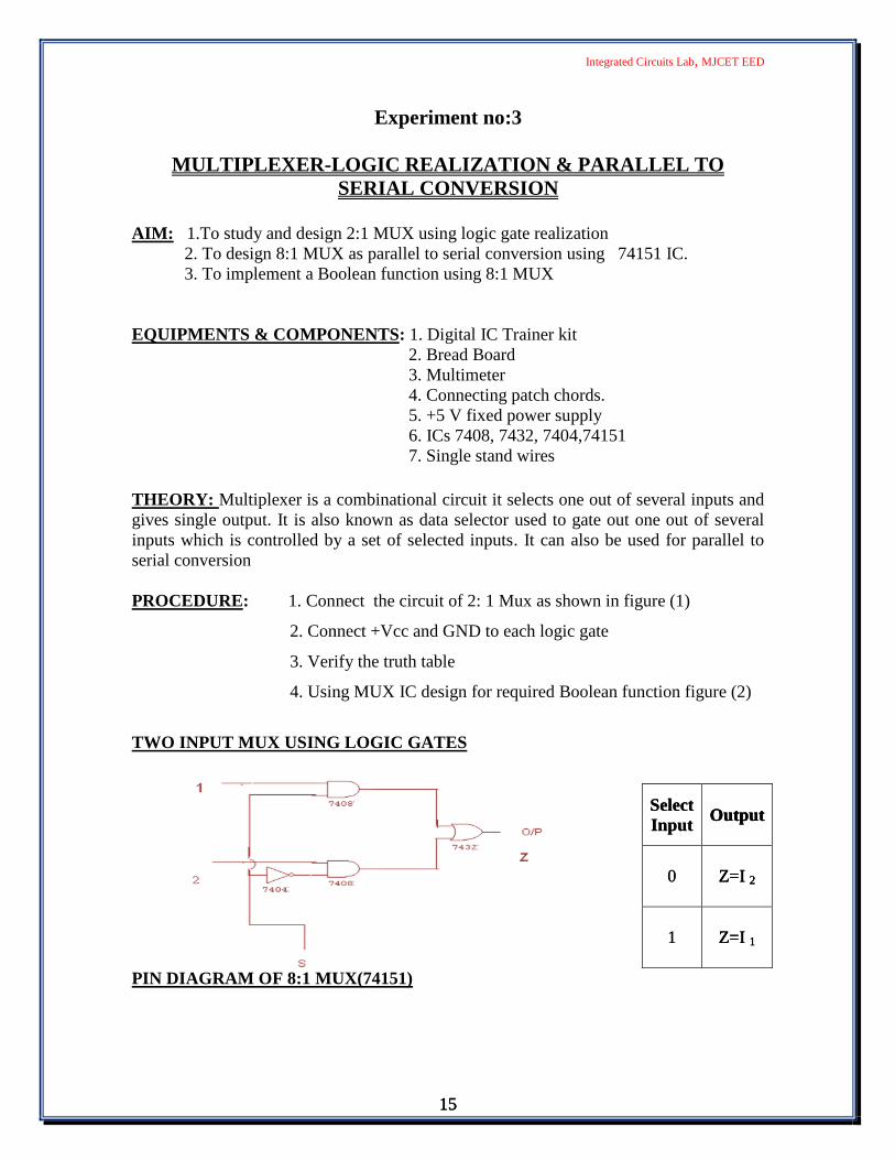
THEORY: Multiplexer is a combinational circuit it selects one out of several inputs andgives single output. It is also known as data selector used to gate out one out of severalinputs which is controlled by a set of selected inputs. It can also be used for parallel toserial conversion
PROCEDURE: 1. Connect the circuit of 2: 1 Mux as shown in figure (1)
2. Connect +Vcc and GND to each logic gate
3. Verify the truth table
4. Using MUX IC design for required Boolean function figure (2)
TWO INPUT MUX USING LOGIC GATES
PIN DIAGRAM OF 8:1 MUX(74151)
SelectInput Output
0 Z=I 2
1 Z=I 1
Integrated Circuits Lab, MJCET EED
15
Experiment no:3
MULTIPLEXER-LOGIC REALIZATION & PARALLEL TOSERIAL CONVERSION
AIM: 1.To study and design 2:1 MUX using logic gate realization2. To design 8:1 MUX as parallel to serial conversion using 74151 IC.3. To implement a Boolean function using 8:1 MUX
EQUIPMENTS & COMPONENTS: 1. Digital IC Trainer kit2. Bread Board3. Multimeter4. Connecting patch chords.5. +5 V fixed power supply6. ICs 7408, 7432, 7404,741517. Single stand wires
THEORY: Multiplexer is a combinational circuit it selects one out of several inputs andgives single output. It is also known as data selector used to gate out one out of severalinputs which is controlled by a set of selected inputs. It can also be used for parallel toserial conversion
PROCEDURE: 1. Connect the circuit of 2: 1 Mux as shown in figure (1)
2. Connect +Vcc and GND to each logic gate
3. Verify the truth table
4. Using MUX IC design for required Boolean function figure (2)
TWO INPUT MUX USING LOGIC GATES
PIN DIAGRAM OF 8:1 MUX(74151)
SelectInput Output
0 Z=I 2
1 Z=I 1
Integrated Circuits Lab, MJCET EED
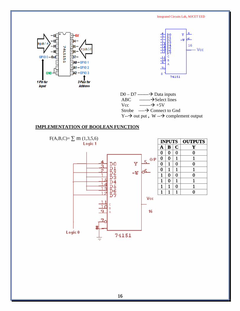
16
D0 – D7 ------- Data inputsABC -------Select linesVcc ------- +5VStrobe ---- Connect to GndY-- out put , W -- complement output
IMPLEMENTATION OF BOOLEAN FUNCTION
F(A,B,C)= ∑ m (1,3,5,6)INPUTS OUTPUTSA B C Y0 0 0 00 0 1 10 1 0 00 1 1 11 0 0 01 0 1 11 1 0 11 1 1 0
Integrated Circuits Lab, MJCET EED
16
D0 – D7 ------- Data inputsABC -------Select linesVcc ------- +5VStrobe ---- Connect to GndY-- out put , W -- complement output
IMPLEMENTATION OF BOOLEAN FUNCTION
F(A,B,C)= ∑ m (1,3,5,6)INPUTS OUTPUTSA B C Y0 0 0 00 0 1 10 1 0 00 1 1 11 0 0 01 0 1 11 1 0 11 1 1 0

Integrated Circuits Lab, MJCET EED
17
DISCUSSION OF RESULT:
Students will be able to observe
1. Implementation of a Boolean function using logic gates & Mux I.C
2. Change in the digital output for various select line changes.
PRELAB QUESTIONS:
1. State difference between Demux & Decoder
2. Applications of Mux & Demux
3. State difference between encoder & Mux

Integrated Circuits Lab, MJCET EED
18
Experiment no:4
TRIANGULAR, SQUARE & SINE WAVE GENERATOR
AIM: 1 To study the operation of triangular wave generator and Design for differentfrequencies2. Compare the theoretical and practical frequencies for different RC Combinations
EQUIPMENTS & COMPONENTS: 1. IC Trainer Kit / Bread board2. Multimeter3. C R O & probes.4. ± 15 V Power supply5. D.C.B6. IC 741(2 nos)7. Resistors 10 K (2 nos)8.50K Pot9.Capacitors 0.047µ F, 0.01µ F
10.Patch chords/connecting wires
THEORY: Figure 1 shows the triangle wave generator using op-amp. The generatorconsists of a comparator A 1 and an integrator A2. The comparator A 1 compares thevoltage at point P continuously with the inverting input that is at 0V. When the voltage atP goes slightly below or above 0V, the output of A 1 is at the negative or positivesaturation level, respectively. To illustrate the circuit's operation, let us set the output ofA 1 at positive saturation +V sat. This +V sat of A 1 and the other is the negative-goingramp of A2. When the negative-going ramp attains a certain value –V ramp, point P isslightly below 0V; hence the output of A 1 will switch from output of A2 will now stopgoing negatively and will begin to go positively. The output of A2 will continue toincrease until it reaches +V ramp. At this time the point P is slightly above 0V; therefore,the output of A 1 is switched back to the positive saturation level +V sat. The sequencethen repeats. The output waveform is as shown in figure 2
The frequencies of the square wave and the triangular wave are the same and is givenby fo = R3/(4R1C1R2) where fo = Output frequencyR1= 10K, R2= 10K
R3= 40K ( Pot variable)
C=0.047µF/ 0.01µ F/0.3 µ F/0.4 µ F
Triangular Vpp =2* * VSat VSat =14v or 15v
Square wave Vpp =2*VSat

Integrated Circuits Lab, MJCET EED
19
PROCEDURE:
1. Connect the circuit as shown in figure (1)
2. Adjust the pot for desired (40K) ,diodes are optional
3. Connect ± 15 V supply to both the 741 ICs
4. connect channel 1 of CRO at the output of A1 and channel 2 at output
of A2
5. Plot the wave forms noting the frequency and amplitude in tabular
column
Figure 1
Integrated Circuits Lab, MJCET EED
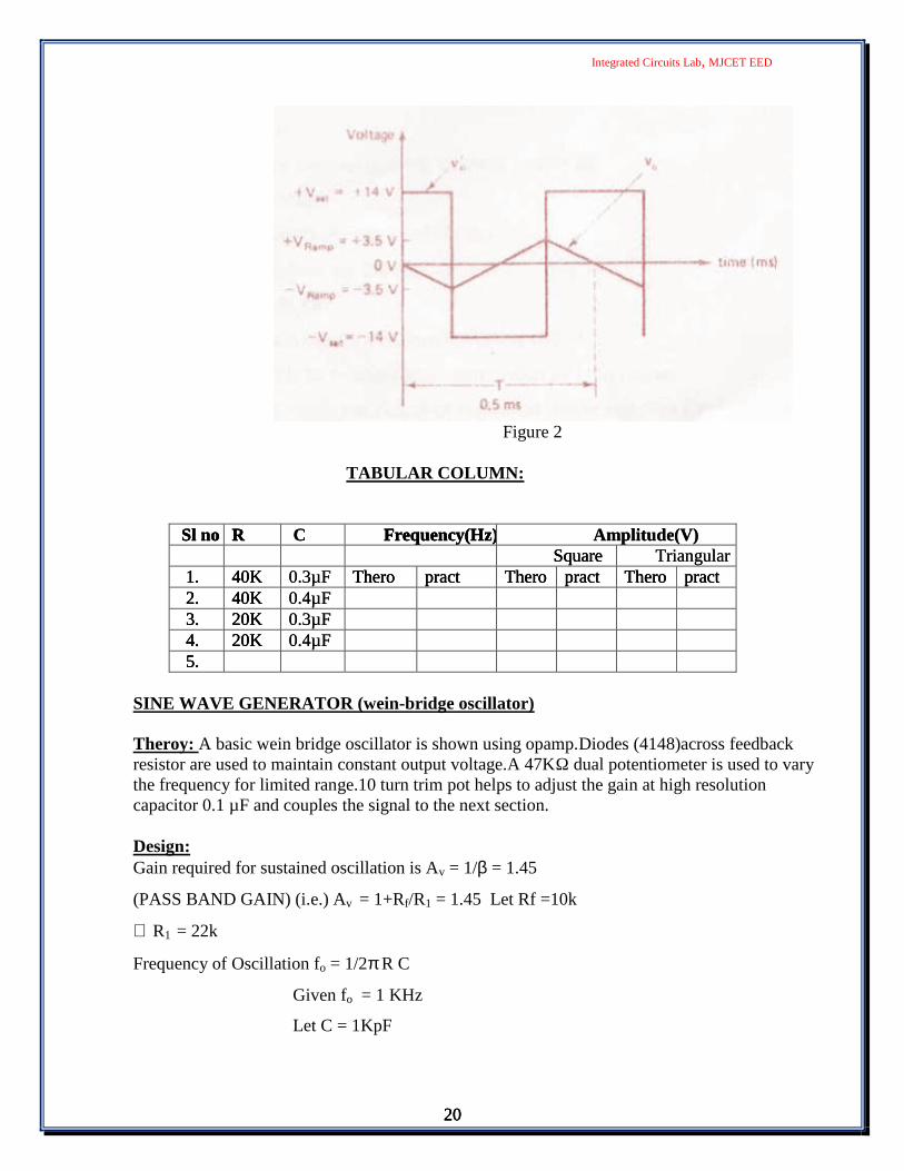
20
Figure 2
TABULAR COLUMN:
Sl no R C Frequency(Hz) Amplitude(V)Square Triangular
1. 40K 0.3µF Thero pract Thero pract Thero pract2. 40K 0.4µF3. 20K 0.3µF4. 20K 0.4µF5.
SINE WAVE GENERATOR (wein-bridge oscillator)
Theroy: A basic wein bridge oscillator is shown using opamp.Diodes (4148)across feedbackresistor are used to maintain constant output voltage.A 47KΩ dual potentiometer is used to varythe frequency for limited range.10 turn trim pot helps to adjust the gain at high resolutioncapacitor 0.1 µF and couples the signal to the next section.
Design:Gain required for sustained oscillation is Av = 1/β = 1.45
(PASS BAND GAIN) (i.e.) Av = 1+Rf/R1 = 1.45 Let Rf =10k
∴ R1 = 22k
Frequency of Oscillation fo = 1/2π R C
Given fo = 1 KHz
Let C = 1KpF
Integrated Circuits Lab, MJCET EED
21
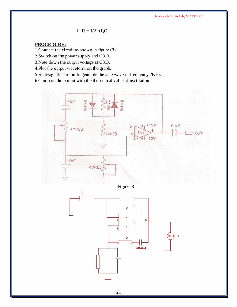
∴ R = 1/2 π foC
PROCEDURE:1.Connect the circuit as shown in figure (3)2.Switch on the power supply and CRO.3.Note down the output voltage at CRO.4.Plot the output waveform on the graph.5.Redesign the circuit to generate the sine wave of frequency 2KHz.6.Compare the output with the theoretical value of oscillation
Figure 3
Integrated Circuits Lab, MJCET EED
21
∴ R = 1/2 π foC
PROCEDURE:1.Connect the circuit as shown in figure (3)2.Switch on the power supply and CRO.3.Note down the output voltage at CRO.4.Plot the output waveform on the graph.5.Redesign the circuit to generate the sine wave of frequency 2KHz.6.Compare the output with the theoretical value of oscillation
Figure 3
Integrated Circuits Lab, MJCET EED
22
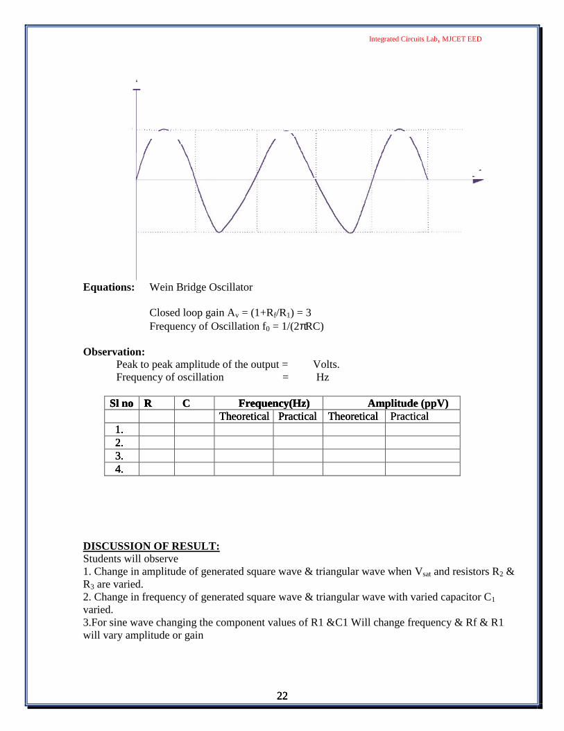
Equations: Wein Bridge Oscillator
Closed loop gain Av = (1+Rf/R1) = 3Frequency of Oscillation f0 = 1/(2πRC)
Observation:Peak to peak amplitude of the output = Volts.Frequency of oscillation = Hz
Sl no R C Frequency(Hz) Amplitude (ppV)Theoretical Practical Theoretical Practical
1.2.3.4.
DISCUSSION OF RESULT:Students will observe1. Change in amplitude of generated square wave & triangular wave when Vsat and resistors R2 &R3 are varied.2. Change in frequency of generated square wave & triangular wave with varied capacitor C1
varied.3.For sine wave changing the component values of R1 &C1 Will change frequency & Rf & R1will vary amplitude or gain
Integrated Circuits Lab, MJCET EED
22
Equations: Wein Bridge Oscillator
Closed loop gain Av = (1+Rf/R1) = 3Frequency of Oscillation f0 = 1/(2πRC)
Observation:Peak to peak amplitude of the output = Volts.Frequency of oscillation = Hz
Sl no R C Frequency(Hz) Amplitude (ppV)Theoretical Practical Theoretical Practical
1.2.3.4.
DISCUSSION OF RESULT:Students will observe1. Change in amplitude of generated square wave & triangular wave when Vsat and resistors R2 &R3 are varied.2. Change in frequency of generated square wave & triangular wave with varied capacitor C1
varied.3.For sine wave changing the component values of R1 &C1 Will change frequency & Rf & R1will vary amplitude or gain

Integrated Circuits Lab, MJCET EED
23
PRELAB QUESTIONS:
1. Do we require any input signal for a square wave generator give reason2. What is the combination of OP-AMP circuits used for generation of Triangular wavegenerator?3. What is the O/P of Integration if positive unit step signal is applied?4. Define Comparator circuit.5. What are the applications of Square & Triangular wave generator circuit?6. How can we increase the amplitude of the o/p square and triangular wave?7. State the two conditions for oscillations.8. Define an oscillator?9. What is the frequency range generated by Wien Bridge Oscillator?

Integrated Circuits Lab, MJCET EED
24
Experiment no:5
ADDERS & SUBTRACTORS-REALIZATION OFCOMBINATIONAL LOGIC
AIM: 1 To study and design Half &Full i) Adders ii) Subtractors Using combinationalLogic gates
EQUIPMENTS & COMPONENTS: 1.. IC Trainer Kit / Bread board2. Multimeter3. 5 V Power supply4. IC 7486(EX-OR), IC 7404 (NOT)5. IC 7408 (AND)6. IC 7432 (OR),8. Single stand wires
THEORY: Half adder is addition of two Boolean Inputs. Used to add two logical inputsA and B. getting the output in sum and carry. Then the Boolean equation for whichoutput ‘1’ is written in sum of product form. Which becomes easier to implement thecircuit. Similarly for a half subtractor we get two outputs difference & borrow Full adderor subtractor has three inputs A ,B,C and only two outputs as shown in below circuits
PROCEDURE: 1. Connect the circuit of half adder using digital trainer kit
2.Connect Vcc and GND for each IC used in circuit
3. Verify the truth table for sum and carry
4. Repeat same for full adder, half subtractor & full subtractor
PIN DIGARMS
NOT Gate NAND/AND/EX-OR Gate

HALF ADDER
Truth table of half adder:
Sum = S = A' B + A B 'Carry = C = A B
FULL ADDER
Truth table for Full adder:
INPUTS OUTPUTSA B SUM CARRY0 0 0 00 1 1 01 0 1 01 1 0 1
HALF ADDER
Truth table of half adder:
Sum = S = A' B + A B 'Carry = C = A B
FULL ADDER
Truth table for Full adder:
INPUTS OUTPUTSA B SUM CARRY0 0 0 00 1 1 01 0 1 01 1 0 1
HALF ADDER
Truth table of half adder:
Sum = S = A' B + A B 'Carry = C = A B
FULL ADDER
Truth table for Full adder:
INPUTS OUTPUTSA B SUM CARRY0 0 0 00 1 1 01 0 1 01 1 0 1
Integrated Circuits Lab, MJCET EED
26
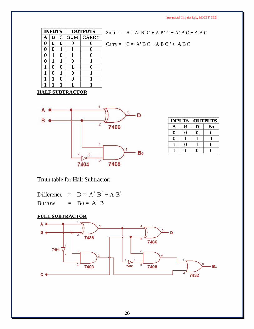
Sum = S = A' B' C + A B' C + A' B C + A B C
Carry = C = A' B C + A B C ' + A B C
HALF SUBTRACTOR
Truth table for Half Subtractor:
Difference = D = A' B' + A B'Borrow = Bo = A' B
FULL SUBTRACTOR
INPUTS OUTPUTSA B C SUM CARRY0 0 0 0 00 0 1 1 00 1 0 1 00 1 1 0 11 0 0 1 01 0 1 0 11 1 0 0 11 1 1 1 1
INPUTS OUTPUTSA B D Bo0 0 0 00 1 1 11 0 1 01 1 0 0
Integrated Circuits Lab, MJCET EED
26
Sum = S = A' B' C + A B' C + A' B C + A B C
Carry = C = A' B C + A B C ' + A B C
HALF SUBTRACTOR
Truth table for Half Subtractor:
Difference = D = A' B' + A B'Borrow = Bo = A' B
FULL SUBTRACTOR
INPUTS OUTPUTSA B C SUM CARRY0 0 0 0 00 0 1 1 00 1 0 1 00 1 1 0 11 0 0 1 01 0 1 0 11 1 0 0 11 1 1 1 1
INPUTS OUTPUTSA B D Bo0 0 0 00 1 1 11 0 1 01 1 0 0

Integrated Circuits Lab, MJCET EED
27
Truth table for Full Subtractor:
Difference = D = A' B' C + A B' C + A B' C ' + A B CBorrow = Bo = A' B' C + A B' C + A' B C + A B C
DISCUSSION OF RESULT: Students will observe implementation of
1. Half & full adders, subtractor using combinational logic gates.2. Half adders full adder Using universal gates
PRELAB QUESTIONS:1. How can we Implement sum of half adder using only one 7400 IC?2. How can we Implement a Not gate using only Nand gates?3. What are universal gates? why are they called so?
INPUTS OUTPUTS
A B C DIFFERENCE BORROW0 0 0 0 00 0 1 1 10 1 0 1 10 1 1 0 11 0 0 1 01 0 1 0 01 1 0 0 01 1 1 1 1
Integrated Circuits Lab, MJCET EED
28
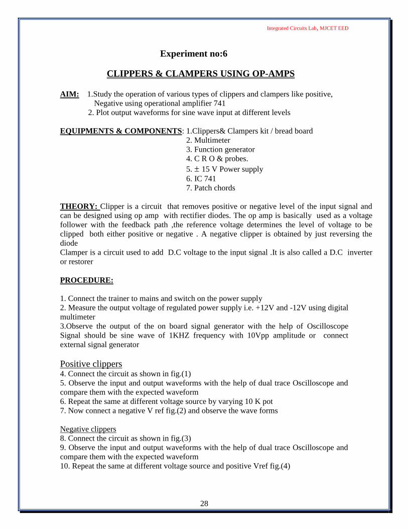
Experiment no:6
CLIPPERS & CLAMPERS USING OP-AMPS
AIM: 1.Study the operation of various types of clippers and clampers like positive,Negative using operational amplifier 741
2. Plot output waveforms for sine wave input at different levels
EQUIPMENTS & COMPONENTS: 1.Clippers& Clampers kit / bread board2. Multimeter3. Function generator4. C R O & probes.5. ± 15 V Power supply6. IC 7417. Patch chords
THEORY: Clipper is a circuit that removes positive or negative level of the input signal andcan be designed using op amp with rectifier diodes. The op amp is basically used as a voltagefollower with the feedback path ,the reference voltage determines the level of voltage to beclipped both either positive or negative . A negative clipper is obtained by just reversing thediodeClamper is a circuit used to add D.C voltage to the input signal .It is also called a D.C inverteror restorer
PROCEDURE:
1. Connect the trainer to mains and switch on the power supply2. Measure the output voltage of regulated power supply i.e. +12V and -12V using digitalmultimeter3.Observe the output of the on board signal generator with the help of OscilloscopeSignal should be sine wave of 1KHZ frequency with 10Vpp amplitude or connectexternal signal generator
Positive clippers4. Connect the circuit as shown in fig.(1)5. Observe the input and output waveforms with the help of dual trace Oscilloscope andcompare them with the expected waveform6. Repeat the same at different voltage source by varying 10 K pot7. Now connect a negative V ref fig.(2) and observe the wave forms
Negative clippers8. Connect the circuit as shown in fig.(3)9. Observe the input and output waveforms with the help of dual trace Oscilloscope andcompare them with the expected waveform10. Repeat the same at different voltage source and positive Vref fig.(4)

Integrated Circuits Lab, MJCET EED
29
Positive clampers11. Connect the circuit as shown in fig.(3)12. Observe the input and output waveforms with the help of dual trace Oscilloscope andcompare them with the expected waveform13. Repeat the same at different voltage source and changing the Vref
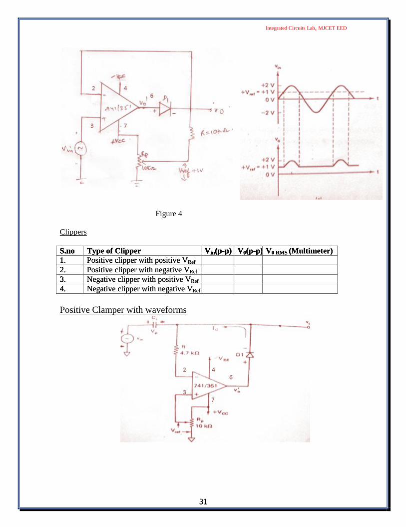
Positive clipper circuit with waveforms for positive V ref
Figure 1
Positive clipper circuit with waveforms for negative V ref
Integrated Circuits Lab, MJCET EED
29
Positive clampers11. Connect the circuit as shown in fig.(3)12. Observe the input and output waveforms with the help of dual trace Oscilloscope andcompare them with the expected waveform13. Repeat the same at different voltage source and changing the Vref
Positive clipper circuit with waveforms for positive V ref
Figure 1
Positive clipper circuit with waveforms for negative V ref

Integrated Circuits Lab, MJCET EED
30
Figure.2Negative Peak clipper with negative V ref wave forms
Figure 3
Negative Peak clipper with positive Reference
Integrated Circuits Lab, MJCET EED
30
Figure.2Negative Peak clipper with negative V ref wave forms
Figure 3
Negative Peak clipper with positive Reference
Integrated Circuits Lab, MJCET EED
30
Figure.2Negative Peak clipper with negative V ref wave forms
Figure 3
Negative Peak clipper with positive Reference
Integrated Circuits Lab, MJCET EED
31
Figure 4
Clippers
S.no Type of Clipper Vin(p-p) V0(p-p) V0 RMS (Multimeter)1. Positive clipper with positive VRef
2. Positive clipper with negative VRef
3. Negative clipper with positive VRef
4. Negative clipper with negative VRef
Positive Clamper with waveforms

Integrated Circuits Lab, MJCET EED
32
Figure 5
Negative Clampers with waveforms
S.no Type of Clamper Vin(p-p) V0(p-p) V0 RMS (Multimeter)1. Positive Clamper with positive VRef
2. Positive Clamper with negative VRef
3. Negative Clamper with positive VRef
4. Negative Clamper with negative VRef
Integrated Circuits Lab, MJCET EED
32
Figure 5
Negative Clampers with waveforms
S.no Type of Clamper Vin(p-p) V0(p-p) V0 RMS (Multimeter)1. Positive Clamper with positive VRef
2. Positive Clamper with negative VRef
3. Negative Clamper with positive VRef
4. Negative Clamper with negative VRef
Integrated Circuits Lab, MJCET EED
32
Figure 5
Negative Clampers with waveforms
S.no Type of Clamper Vin(p-p) V0(p-p) V0 RMS (Multimeter)1. Positive Clamper with positive VRef
2. Positive Clamper with negative VRef
3. Negative Clamper with positive VRef
4. Negative Clamper with negative VRef

Integrated Circuits Lab, MJCET EED
33
DISCUSSION ON RESULT: Students will observe that1. As the reference voltage through Pot changes the clipping & clamping limit of wave changes2. Polarity of diode position will decide positive or negative clipper & clamper3. Positive or negative Vref of clipper or clamper is decided by DC biasing voltage connected to
biasing pins of op amps
PRELAB QUESTIONS:1. Why clamper is called a DC restorer?2. What are the applications of clippers and clampers?3. What is the factor which determines clipping level in a clipper?

Integrated Circuits Lab, MJCET EED
34
Experiment no:7
DESIGN OF INTEGRATOR & DIFFERENTIATOR
AIM: 1. To design and demonstrate the operation of a practical Differentiator &Integrator using op-amp2. To plot differentiated and integrated outputs for different input waveforms
EQUIPMENTS & COMPONENTS:1. Digital IC Trainer kit / bread board2. Multimeter3. Function generator4. C R O & probes.5. ± 15 V Power supply6. IC 7417. Resistors 4.7K,10 K8. Capacitors 0.01µ F9. Single Stand Wires10. Decade Capacitance .Box11. Decade Resistance .Box
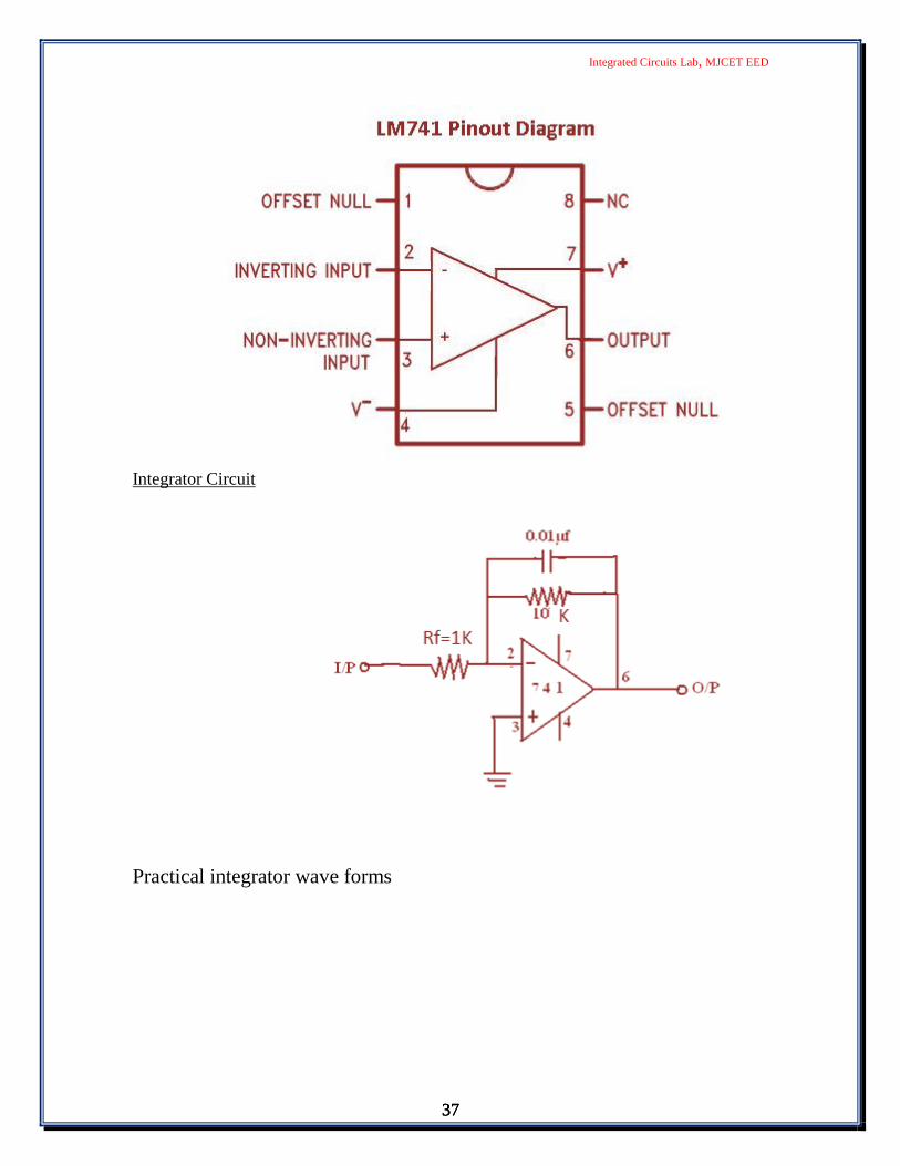
THEORY:Integrator: A circuit in which the output voltage is the integration of the input voltage is called anintegrator. In the practical integrator to reduce the error voltage at the output, a resistor RF isconnected across the feedback capacitor CF.
Thus, RF limits the low-frequency gain and hence minimizes thevariations in the output voltage.
Integrated Circuits Lab, MJCET EED
34
Experiment no:7
DESIGN OF INTEGRATOR & DIFFERENTIATOR
AIM: 1. To design and demonstrate the operation of a practical Differentiator &Integrator using op-amp2. To plot differentiated and integrated outputs for different input waveforms
EQUIPMENTS & COMPONENTS:1. Digital IC Trainer kit / bread board2. Multimeter3. Function generator4. C R O & probes.5. ± 15 V Power supply6. IC 7417. Resistors 4.7K,10 K8. Capacitors 0.01µ F9. Single Stand Wires10. Decade Capacitance .Box11. Decade Resistance .Box
THEORY:Integrator: A circuit in which the output voltage is the integration of the input voltage is called anintegrator. In the practical integrator to reduce the error voltage at the output, a resistor RF isconnected across the feedback capacitor CF.
Thus, RF limits the low-frequency gain and hence minimizes thevariations in the output voltage.

Integrated Circuits Lab, MJCET EED
35
Figure1 :Frequency response of integrator
The frequency response of the integrator is shown in the above fig. fb is the frequency atwhich the gain is 0 dB and is given by fb = 1/2πR1Cf.
In this fig. there is some relative operating frequency, and for frequencies from f to fa the gainRF/R1 is constant. However, after fa the gain decreases at a rate of 20 dB/decade. In other words,between fa and fb the circuit of fig. 2.1 acts as an integrator. The gain-limiting frequency fa isgiven by fa = 1/2π RfCf. Normally fa<fb. From the above equation, we can calculate Rf byassuming fa & Cf. This is very important frequency. It tells us where the useful integration rangestarts. If fin < fa - circuit acts like a simple inverting amplifier and no integration results, If fin = fa -integration takes place with only 50% accuracy results, If fin = 10fa - integration takes place with99% accuracy results. In the circuit diagram of Integrator, the values are calculated by assumingfa as 50 Hz. Hence the input frequency is to be taken as 500Hz to get 99% accuracy results.
Design Aspects for Integrator: Design for a practical circuit with D.C gain of 20 tointegrate a signal of maximum frequency 2KHz.
Steps For Design:
1.The D.C gain for the practical integrator is |A| dc =₁. Choose Rf=100KΩ R1=5 KΩ
(use R0=4.7KΩ)
2. Condition for Proper integrator I/P frequency f >10fa.fa → break frequency. f/fa= 10=> fa=200 Hz.
fa = 1/2 RfCf.Choose Cf=0.01µf. ∴Rf=79.5 KΩ. (use Rf=100KΩ)NOTE: For f < fa circuit behaves as an inverting amplifier & output
V0 = Rf/R1.Vin.
For f > fa circuit in an integrator & output Vo = 1/R1C₁∫ in dt.
Differentiator:As the name suggests, the circuit performs the mathematical operation of differentiation,i.e. the output voltage is the derivative of the input voltage.
Vo = - Rf C1
Both the stability and the high-frequency noise problems can be corrected by the additionof two components: R1 and Cf, as shown in the circuit diagram.This circuit is a practical differentiator. The input signal will be differentiated properly ifthe time period T of the input signal is larger than or equal to RfC1. That is, T>= RfC1

Integrated Circuits Lab, MJCET EED
36
Differentiator can be designed by Selecting fa equal to the highest frequency of the inputsignal to be differentiated. Then, assuming a value of C1<1 F, calculate the value of Rf .Calculate the values of R1and Cf so that R1C1=RfCf.
Design Aspects For Differentiator: Design for a practical differentiator circuit that willdifferentiate an Input signal with maximum frequency 2 KHz.
Steps For Design:1. Choose fa=fmax=2kHz.2. Choose C1=0.01µf. Now fa=1 2 f 1 Rf=1 2 f 1=7.9KΩ (use 10 KΩ).3. Now fb=2fa ( fa<f b) & R1C1=RfCf fb=1 2 f 1∴ R1=3.9KΩ (use 4.7KΩ)& R1C1=Rf
Cf=5 nf.
PROCEDURE:
1. Connect the integrator circuit as per design. Adjust the function generator to produce 2
volts P/P sine wave of 1 KHz.
2. Observe input & output simultaneously on the CRO. Measure & record the peak value
of Vo & the phase angle of Vo with repeat Vi.
3. Repeat step (2) while increasing the frequency of I/P signal. Find the maximum
frequency at which circuit performs integration. Compare with calculated value of fa.
4. Now set function generator to 2V P/P square wave of 1 KHz to get the O/P of a
triangle waveform. Plot the amplitude & frequency on a graph sheet
5. Similarly connect differentiator circuit verify that for inputs of sine wave and square
wave we get outputs of cosine wave & spike wave respectively
NOTE: The O/P amplitude of differentiator is directly proportional to the I/P frequency
Integrated Circuits Lab, MJCET EED
37
Integrator Circuit
Practical integrator wave forms
Integrated Circuits Lab, MJCET EED
37
Integrator Circuit
Practical integrator wave forms
Integrated Circuits Lab, MJCET EED
37
Integrator Circuit
Practical integrator wave forms
Integrated Circuits Lab, MJCET EED
38
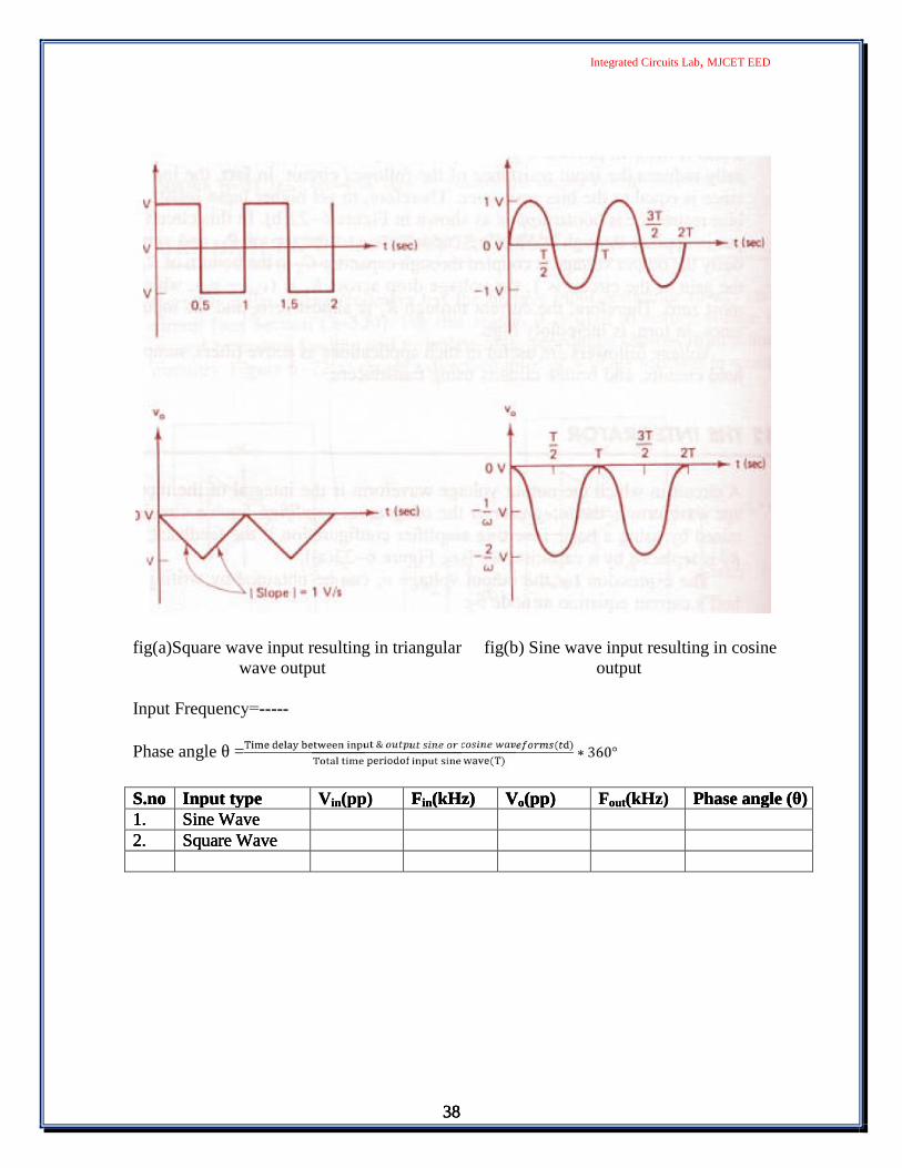
fig(a)Square wave input resulting in triangular fig(b) Sine wave input resulting in cosinewave output output
Input Frequency=-----
Phase angle θ = & ( )( ) ∗ 360°S.no Input type Vin(pp) Fin(kHz) Vo(pp) Fout(kHz) Phase angle (θ)1. Sine Wave2. Square Wave
Integrated Circuits Lab, MJCET EED
38
fig(a)Square wave input resulting in triangular fig(b) Sine wave input resulting in cosinewave output output
Input Frequency=-----
Phase angle θ = & ( )( ) ∗ 360°S.no Input type Vin(pp) Fin(kHz) Vo(pp) Fout(kHz) Phase angle (θ)1. Sine Wave2. Square Wave
Integrated Circuits Lab, MJCET EED
38
fig(a)Square wave input resulting in triangular fig(b) Sine wave input resulting in cosinewave output output
Input Frequency=-----
Phase angle θ = & ( )( ) ∗ 360°S.no Input type Vin(pp) Fin(kHz) Vo(pp) Fout(kHz) Phase angle (θ)1. Sine Wave2. Square Wave
Integrated Circuits Lab, MJCET EED
39
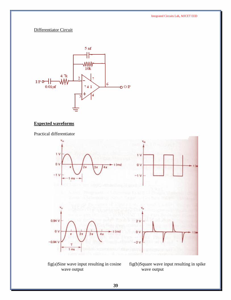
Differentiator Circuit
Expected waveforms
Practical differentiator
fig(a)Sine wave input resulting in cosine fig(b)Square wave input resulting in spikewave output wave output
Integrated Circuits Lab, MJCET EED
39
Differentiator Circuit
Expected waveforms
Practical differentiator
fig(a)Sine wave input resulting in cosine fig(b)Square wave input resulting in spikewave output wave output
Integrated Circuits Lab, MJCET EED
39
Differentiator Circuit
Expected waveforms
Practical differentiator
fig(a)Sine wave input resulting in cosine fig(b)Square wave input resulting in spikewave output wave output

Integrated Circuits Lab, MJCET EED
40
S.no Input type Vin(pp) Fin(kHz) Vo(pp) Fout(kHz) Phase angle (θ)1. Sine Wave2. Square Wave
DISCUSSION ON RESULT: Students will be able to observe1. Practical integrator response changes for maximum frequency design F max with respect to
Feedback resistor Rf2. Practical Differentiator response depends on resistor R1 & capacitor Cf.3. As input frequency is increased in integrator output voltage decreases and in differentiatoroutput voltage increases
PRELAB QUESTIONS:1. What are the Ideal characteristics of an op amp?2. Define slew rate and what happens if it is very less?3. What are the functions of pin 1 &5 in op amp IC 741?4. What are the different applications of integrator and differentiator?5. What are the advantages of practical integrator & differentiator compared with their idealcircuits?
Integrated Circuits Lab, MJCET EED
41
Experiment no:8
PHASE LOCKED LOOP
AIM: To design PLL Circuit for required Oscillating, Capture & lock Frequencies
EQUIPMENTS & COMPONENTS: 1. PLL Trainer board2. Dual trace oscilloscope3. Digital frequency counters4. Digital multimeter
THEORY: A PLL is basically a closed loop feedback system. The basic purpose of the PLL isto synchronize the frequency of the voltage controlled oscillator with that of the incoming signal,It goes through the following three stages
Free running: When the control voltage given as input to the VCO Is zero, then VCO is said tobe in free running mode
Capture: When the control voltage is applied as input to VCO, which forces the VCO to changeits output frequency to move towards the frequency of the incoming signal until the twofrequencies become equal is called capturing
Locked: when two frequencies (Input & Output) are equal ,then circuit is said to be locked .Thetotal time taken by PLL to establish lock is called as pull in time
Free Running Frequency, FO =.
, Ct = 0.01µF, Rt=6 KΩ
Capture Frequency, FC =
Locked Frequency, FL =± ,VCC =+ VCC –(- VCC)
Integrated Circuits Lab, MJCET EED
42
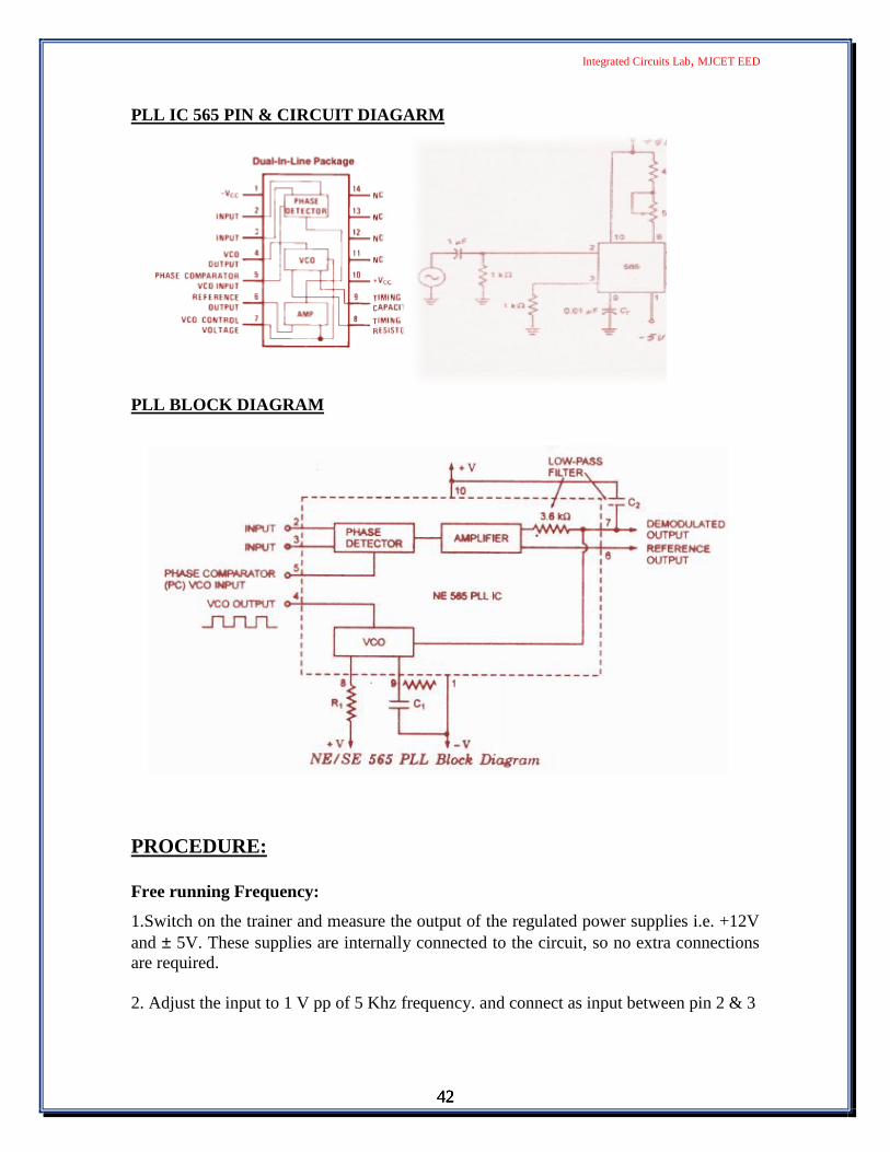
PLL IC 565 PIN & CIRCUIT DIAGARM
PLL BLOCK DIAGRAM
PROCEDURE:
Free running Frequency:
1.Switch on the trainer and measure the output of the regulated power supplies i.e. +12Vand ± 5V. These supplies are internally connected to the circuit, so no extra connectionsare required.
2. Adjust the input to 1 V pp of 5 Khz frequency. and connect as input between pin 2 & 3
Integrated Circuits Lab, MJCET EED
42
PLL IC 565 PIN & CIRCUIT DIAGARM
PLL BLOCK DIAGRAM
PROCEDURE:
Free running Frequency:
1.Switch on the trainer and measure the output of the regulated power supplies i.e. +12Vand ± 5V. These supplies are internally connected to the circuit, so no extra connectionsare required.
2. Adjust the input to 1 V pp of 5 Khz frequency. and connect as input between pin 2 & 3

Integrated Circuits Lab, MJCET EED
43
3.Calculate the free-running frequency range of the circuit for different values of timingresistor Rt (to measure the Rt—Switch off the trainer and measure the Rt value usingdigital multimeter between two given test points) and record the frequency values intable1
4. Connect 0.1µf capacitor (CC) to the circuit and open the loop by short between pin 4and pin5. Measure the minimum and maximum free-running frequencies obtainable at theoutput of the PLL (pin4) by varying the pot. Compare your results with your calculationsfrom step 3 (theoretical value). Simultaneously you can observe the output signal usingCRO.
Lock Range:
5. Calculate the lock range of the circuit for a 5 kHz free-running frequency and record intable 2.
6. Connect pin 4, 5 with the help of springs and adjust potentiometer to get a free-runningfrequency of 5 kHz. Connect square wave generator output to the input of the PLLcircuit. Provide a 5 kHz square signal of 1Vpp approximately (make this input frequencyas close to the VCO frequency as possible).
7. Connect the frequency counters or CRO both channels to the input and output of thePLL.
8. Observe input and output frequencies while slowly increasing the frequency of squarewave at the input. For some range output and input are equal this known as locking andPLL said to be lock with the input signal. Record the frequency at which the PLL breakslock (output frequency of the PLL will be around VCO frequency and in oscilloscope youwill see a jittery waveform when it breaks lock instead of clean square wave). Thisfrequency is called the upper end of lock range and records this as F2.
9.Beginning at 5khz slowly decrease the frequency of the input and determine thefrequency at which the PLL breaks lock on the low end and record it as F1.
10. Find lock range from F2-F1 and compare with the theoretical values from step5.
Note:-C2 (Filter capacitor) is used to eliminate possible oscillation in the VCO voltage
Capture range:
11.Calculate the capture range of the circuit for a 5 kHz free-running frequency (considerfilter capacitor Cc) is 0.1µf.
12.With the oscilloscope and counter still on pin4, slowly increase the input frequencyfrom minimum (say 1 kHz). Record frequency (as F3) at which the input and outputfrequencies of the PLL equal, this is known as lower end of the capture range.

Integrated Circuits Lab, MJCET EED
44
13.Now keep input frequency at maximum possible (say 10 kHz) and slowly reduce andrecord known as upper end of the capture range.
14.Find capture range from F4-F3 and compare it with the theoretical value (from step 10).
15.Repeat the step from 10 to 13 Cc value 0.2µf.
Table 1 Free-running Frequency (F o)
Ct =0.01µF
S.no Rt (Pot)value
Theoreticalfrequency(F0) KHz
Practicalfrequency(F0) KHz
1. 5KΩ2. 6KΩ
Table 2 for Lock range( F L)S.no Rt (Pot)
valueTheoretical
frequency(FL) KHzPractical
frequency(FL) KHzF1 F2 F1 F2
1. 5KΩ2. 6KΩ
Table 3 for Capture range (FC)
Filter Capacitor C f = 0.1µF
S.no Rt (Pot)Value
Theoreticalfrequency(FC) KHz
Practicalfrequency(FC) KHz
F3 F4 F3 F4
1. 5KΩ2. 6KΩ
SAMPLE CALCULATIONS:
i) Free-running Frequency FO =.
, for Ct = 0.01µF, Rt=5 KΩ

Integrated Circuits Lab, MJCET EED
45
= 6Khz
ii) Locked Frequency, ΔFL =± ,VCC =+ VCC –(- VCC )
= +5-(-5) =10v
=± × ×= ± 4.8 Khz
F1= FO +ΔFL F2= FO -ΔFL
=6+4.8 =6-4.8=10.8 kHz =1.2 kHz
iii) Capture Frequency, ΔFC = ±
where = 3.6 Ω, = 0.1µΔFC = ± 1.45Khz
Note : F L > F c
NATURE OF GRAPH:
DICUSSION ON RESULT: Students will be able to observe1.That oscillating frequency of PLL decides the capture & lock frequencies2.Response of filter is varied if capacitor Cf & Rf is changed
PRELAB QUESTIONS:
1.Define lock range ,capture range & free running frequency for PLL2.What are the applications of PLL?3.What is VCO what is its output ?4.What is the function of phase detector

Integrated Circuits Lab, MJCET EED
46
Experiment no:9
SYNCHRONOUS COUNTERS
AIM: 1. To design and study a synchronous counter using 7490 I.C2. Design a Mod 10 & Mod 6 counter
EQUIPMENTS & COMPONENTS: 1.Digital IC Trainer Kit2.Multimeter3.Connecting patch chords.4.+ 5V Power supply5. IC 74906.7408 AND Gate IC7.Single Stand Wires
THEORY:7490 consists of four flip-flops internally connected to provide a mod 2counter and a mod 8 counter can be used independently or in combination. Flip-flop Aoperates as a mod 2 counter where as the combination of flip-flop B, flip-flop C, Flip-flop D form a mod 8 counter.
There are two reset inputs R1 and R2 both of which are to be connected to logic 1for clearing all the flip-flops.The two set inputs S1 and S2 when connected to logic 1 areused for setting the counter to 1001.
PIN DIAGRAM 7490 :

Integrated Circuits Lab, MJCET EED
47
CIRCUIT DIAGRAM:
PROCEDURE:1. Connect the circuit of 7490 for BCD count as shown in the circuit.
2. Observe the full count of mod 10.
3. Using AND gate design a mod-6 and mod-5 counter.
4. Short Reset pin to the output of AND gate.
5. Verify corresponding MOD count
MOD – 10

Integrated Circuits Lab, MJCET EED
48
Design mod-6 B.C.D Counter using I.C 7490
State QD QC QB QA
0 0 0 0 01 0 0 0 12 0 0 1 03 0 0 1 14 0 1 0 05 0 1 0 16 60 0 0 0
Integrated Circuits Lab, MJCET EED
48
Design mod-6 B.C.D Counter using I.C 7490
State QD QC QB QA
0 0 0 0 01 0 0 0 12 0 0 1 03 0 0 1 14 0 1 0 05 0 1 0 16 60 0 0 0
Integrated Circuits Lab, MJCET EED
48
Design mod-6 B.C.D Counter using I.C 7490
State QD QC QB QA
0 0 0 0 01 0 0 0 12 0 0 1 03 0 0 1 14 0 1 0 05 0 1 0 16 60 0 0 0

Integrated Circuits Lab, MJCET EED
49
Design mod-7 B.C.D Counter using I.C 7490 Truth Table:MOD-7
DICUSSION ON RESULT: Students will observe
1. When AND gate is connected ,the count of synchronous counter resets2. Synchronous counter of any mod value can be implemented using reset pins connected
to respective output terminals
PRELAB QUESTIONS: 1.Define synchronous counter2. What is a ripple counter?3. Why do we use AND gate to reset?
State QD QC QB QA
0 0 0 0 01 0 0 0 12 0 0 1 03 0 0 1 14 0 1 0 05 0 1 0 16 60 1 1 07 0 0 0 0

Integrated Circuits Lab, MJCET EED
50
Experiment no:10
ASYNCHRONOUS COUNTERS
AIM: 1. To design and study a 4 bit Asynchronous counter using flip flop I.C2. Design Mod 12 asynchronous counter using 7473 flip-flops
EQUIPMENTS & COMPONENTS: 1. Digital IC Trainer kit2. Multimeter3. Connecting patch chords.4. + 5V Power supply5. IC 7473 (2 nos)6.7400 NAND Gate IC7. Single Stand Wires
THEORY: Give the maximum count the number of flip-flops required will be N=2 n
Here the output of previous flip flop acts as clock input to the next flip Flop. Thusincreasing the propagation time. Nand gate is used to reset count
Procedure:1.Connect all flip-flops as a ripple counter as shown in figure (1)
2.Find the binary number for last state is reset state.
3.Connect all the flip-flops outputs that are 1 at the last state as the inputs to the NAND
gates.
4. Connect the NAND gate output to the clear input of all flip-flops.
5. Switch Power ON and verify that it reads 0 to 15 [0000 to 1111] after 1111 it again
resets 0000.
6. Later for fig ( 2 ) connections it reads 0 to 11 [0000 to 1011] after 1011 it again resets
0000. Therefore cycle of 0000 to 1011 repeats.
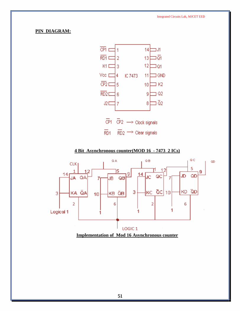
Integrated Circuits Lab, MJCET EED
51
PIN DIAGRAM:
4 Bit Asynchronous counter(MOD 16 - 7473 2 ICs)
Implementation of Mod 16 Asynchronous counter
Integrated Circuits Lab, MJCET EED
51
PIN DIAGRAM:
4 Bit Asynchronous counter(MOD 16 - 7473 2 ICs)
Implementation of Mod 16 Asynchronous counter
Integrated Circuits Lab, MJCET EED
51
PIN DIAGRAM:
4 Bit Asynchronous counter(MOD 16 - 7473 2 ICs)
Implementation of Mod 16 Asynchronous counter
Integrated Circuits Lab, MJCET EED
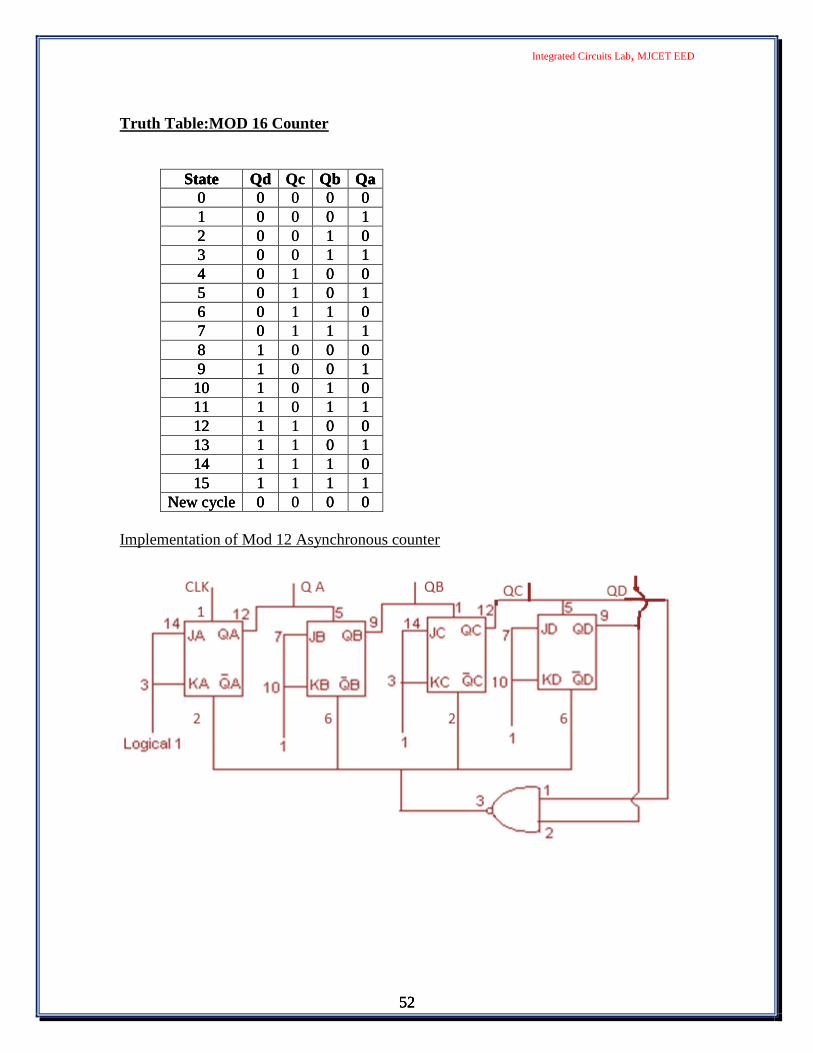
52
Truth Table:MOD 16 Counter
State Qd Qc Qb Qa0 0 0 0 01 0 0 0 12 0 0 1 03 0 0 1 14 0 1 0 05 0 1 0 16 0 1 1 07 0 1 1 18 1 0 0 09 1 0 0 1
10 1 0 1 011 1 0 1 112 1 1 0 013 1 1 0 114 1 1 1 015 1 1 1 1
New cycle 0 0 0 0
Implementation of Mod 12 Asynchronous counter
Integrated Circuits Lab, MJCET EED
52
Truth Table:MOD 16 Counter
State Qd Qc Qb Qa0 0 0 0 01 0 0 0 12 0 0 1 03 0 0 1 14 0 1 0 05 0 1 0 16 0 1 1 07 0 1 1 18 1 0 0 09 1 0 0 1
10 1 0 1 011 1 0 1 112 1 1 0 013 1 1 0 114 1 1 1 015 1 1 1 1
New cycle 0 0 0 0
Implementation of Mod 12 Asynchronous counter
Integrated Circuits Lab, MJCET EED
52
Truth Table:MOD 16 Counter
State Qd Qc Qb Qa0 0 0 0 01 0 0 0 12 0 0 1 03 0 0 1 14 0 1 0 05 0 1 0 16 0 1 1 07 0 1 1 18 1 0 0 09 1 0 0 1
10 1 0 1 011 1 0 1 112 1 1 0 013 1 1 0 114 1 1 1 015 1 1 1 1
New cycle 0 0 0 0
Implementation of Mod 12 Asynchronous counter

Integrated Circuits Lab, MJCET EED
53
Truth Table:MOD 12 Counter
State Qd Qc Qb Qa0 0 0 0 01 0 0 0 12 0 0 1 03 0 0 1 14 0 1 0 05 0 1 0 16 0 1 1 07 0 1 1 18 1 0 0 09 1 0 0 1
10 1 0 1 011 1 0 1 112 1 1 0 0
New cycle 0 0 0 0
DISCUSSION ON RESULT: Students will observe1. When NAND gate is connected the count of asynchronous counter resets2. Asynchronous counter of any mod value can be implemented using reset pins
connected to respective output terminals using flip flops
PRELAB QUESTIONS:1. What is a decade counter?2. Compare asynchronous and synchronous counters3. Define propagation delay.4. Mention Differences between a flip flop and latch

Integrated Circuits Lab, MJCET EED
54
Experiment no:11
D/A CONVERTER- R-2R LADDER
AIM: To study and obtain the practical analog output for a 4-bit R-2R ladder type DACusing op-amp.
EQUIPMENTS & COMPONENTS: 1. Op-amp IC 7412. Resistors 1KΩ,2KΩ3. Dual Power Supply ±15V4. Multimeter5. CRO6. Connecting wires
THEORY:-In R-2R ladder type D to A converter, only two values of resistors is used(i.e. R and 2R). The typical values of R are from 2.5KΩ to 10KΩ. In this output voltageis a weighted sum of digital inputs. Since the resistive ladder is a linear network, theprinciple of super position can be used to find the total analog output voltage for aparticular digital input by adding the output voltages caused by the individual digitalinputs.
Circuit Diagram:-

Integrated Circuits Lab, MJCET EED
55
PROCEDURE:
1. Switch on the D/A Trainer kit.2. Connect the four logical inputs provided on the kit to A, B, C, D terminals.3. Connect the ladder network output to the input of the summing amplifier.4. Connect the multimeter to the output of summing amplifier.5. Set the offset voltage to zero by using zero adjustment pot with zero input (betweenpin 2 and GND).6. By keeping input at logic 1 (LSB 0001) adjust the gain to some constant voltage. Forexample 0.25V or 0.5V.7. By varying the logical inputs observe the output increasing according to the input.8. Apply the clock to the input of decade counter and observe the output on CRO.
(Connect ABCD of R-2R ladder network to counter QA, QB, QC & QD)
9. Observe the Stair case waveform on CRO and calculate the resolution.10. Draw the graph between Analog equivalent of digital input Vs Analog output andobserve the linearity.
TABULAR COLUMN:
S.No Digital Input
D C B A
Analog Output(Theoritical)(in Volts)
Analogequivalent ofDigital input(in Volts) ‘∆’
Analog Output(in Volts)
‘E’
1 0 0 0 02 0 0 0 13 0 0 1 04 0 0 1 15 0 1 0 06 0 1 0 17 0 1 1 08 0 1 1 19 1 0 0 0
10 1 0 0 111 1 0 1 012 1 0 1 113 1 1 0 014 1 1 0 115 1 1 1 016 1 1 1 1

Integrated Circuits Lab, MJCET EED
56
EXPECTED WAVEFORM:
Calculations:
(1)
+++−=
424
323
222
121 bbbb
RfR
RVoV
Where Reference Voltage, VR=5V (given)b1 = D, b2 = C, b3 = B & b4 = A
(2) Resolution, Res = 1/ (2n-1)
Where ‘n’ is no. of bits.
(3) Linearity Error (LE): It is the difference between expected output and actualoutput.
% LE = (E-∆) x 100
DISCUSSION OF RESULT:- Students will observe and discuss1.Linearity and resolution of DAC2.Output response step wise for various digital inputs changes for change in resolution
PRELAB QUESTIONS:
1. Mention any two specifications of a DAC.2. Name any two types of DAC.3. Advantages & Disadvantages of R-2R ladder DAC over Binary weighted DAC4. Define resolution, monotonicity and accuracy with respect to DAC.5. What is the range value for resistor (R) in DAC?

Integrated Circuits Lab, MJCET EED
57
Experiment no:12
A/D CONVERTER
AIM: To study the operation of an 8 bit SAR type ADC and compare the theoretical and
practical digital outputs.
EQUIPMENTS & COMPONENTS: 1. ADC 0808 IC
2. Connecting wires
3. Digital Multimeter
4. Trainer kit
THEORY:Analog to Digital converters are used in all computer applications that require interface
with the analog world. In addition, if a digital read out of an analog measurement is
needed, a stand-alone ADC can be used to generate the bit patterns required to drive a
decimal or hexadecimal display. The ADC0808 ADC0809 data acquisition component is a
monolithic CMOS device with an 8-bit Analog-to-digital converter, 8-channel multiplexer
and Microprocessor compatible control Logic The 8-bit A/D converter uses successive
approximation as the conversion technique. The converter features a high impedance chopper
stabilized Comparator a 256R voltage divider with Analog Switch tree and a successive
approximation Register The 8-channel multiplexer can directly access any of 8-single-
ended Analog signals.
PROCEDURE:1.Connect clock pulse to the clock input of IC ADC 0808 to apply analog signal.
2.Connect multimeter across analog signal .
3.Switch power supply
4.Now increase the analog input voltage using knob in steps of 0.5V.
5.Measure the two voltages Va and VR using digital multimeter.
6.Verify the digital output by observing LEDs & tabulate them
7.Compare theoretical and practical values.
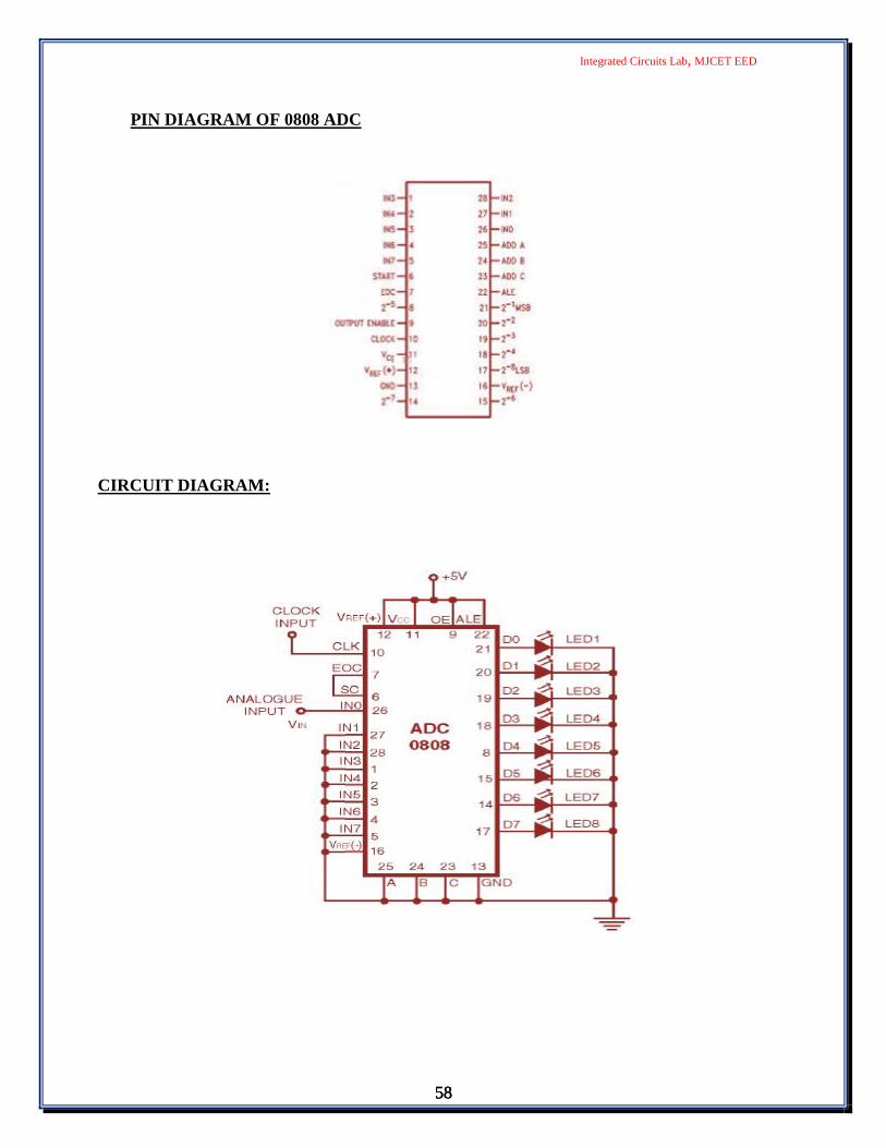
Integrated Circuits Lab, MJCET EED
58
PIN DIAGRAM OF 0808 ADC
CIRCUIT DIAGRAM:
Integrated Circuits Lab, MJCET EED
58
PIN DIAGRAM OF 0808 ADC
CIRCUIT DIAGRAM:
Integrated Circuits Lab, MJCET EED
58
PIN DIAGRAM OF 0808 ADC
CIRCUIT DIAGRAM:

Integrated Circuits Lab, MJCET EED
59
TABULAR COLUMN:
S.no
I/pV
O/p V Digital output Theoretical Digital output display
1 0 D7 D6 D5 D4 D3 D2 D1 D0 D7 D6 D5 D4 D3 D2 D1 D0
2 0.5
3 1
4 1.5
5 2
6 2.5
7 3
8 3.5
9 4
10 4.5
11 5
DISCUSSION ON RESULT: Students will observe
1.Successive approximation register A to D Converter specifications practically
2.Change in digital output for various analog input ranges .
PRELAB QUESTIONS:
1. What are the different specifications of a ADC ?.
2. Name different types of ADC.
3. What are the Advantages & Disadvantages of SAR Type ADC over Dual
Slope type ADC?.
4. What are the Advantages of DAC over ADC ?.
Integrated Circuits Lab, MJCET EED
60
Experiment no:13
MONOSTABLE MULTIVIBRATOR USING IC 555
AIM: To study the operation of a Monostable multivibrator using 555 IC
EQUIPMENTS & COMPONENTS:1.C.R.O
2.Function generator
3. Multimeter
4.Bread board
5. ± 15 V variable power supply
6. 555 Timer IC
7. Resistors 10k
8. Capacitors 0.1µF,0.01µF(2)
9.Single stand wires
THEORY: Monostable Multivibrators has one stable state and other is a quasi stable
state. The circuit is useful for generating single output pulse at adjustable time duration in
response to a triggering signal. The width of the output pulse depends only on external
components, resistor and a capacitor.
The stable state is the output low and quasi stable state is the output high. In thestable state transistor Q1 is ‘on’ and capacitor C is shorted out to ground. However uponapplication of a negative trigger pulse to pin2, Q1 is turned ‘off’ which releases the shortcircuit across the external capacitor C and drives the output high. The capacitor C nowstarts charging up towards Vcc through RA. However when the voltage across C equal 2/3Vcc the upper comparator output switches form low to high which in turn drives theoutput to its low state via the output of the flip flop. At the same time the output of theflip flop turns Q1 ‘on’ and hence C rapidly discharges through the transistor. The outputremains low until a trigger is again applied. Then the cycle repeats.
The pulse width of the trigger input must be smaller than the expected pulse widthof the output. The trigger pulse must be of negative going signal with amplitude largerthan 1/3 Vcc. The width of the output pulse is given by,
T = 1.1 RAC

Integrated Circuits Lab, MJCET EED
61
Figure 2: Waveforms for IC555 Monostable Multivibrator
Note:Once triggered, the circuits output will remain in the high state until the set time tpelapses. The output will not change its state even if an input trigger is applied againduring this time interval tp.

Integrated Circuits Lab, MJCET EED
62
DESIGN:
Given a pulse width of duration of 100 µs
Let C = 0.01 µF; Frequency = _________KHz
Here, T= 1.1 RAC
So,calculate RA =
PROCEDURE:
1. Rig-up the circuit of 555 monostable Multivibrators as shown in fig with the
designed value of components.
2. Connect the trigger input to pin 2 of 555 timer form the function generator.
3. Connect the CRO probes to pin 3 and 2 to display the output signal and the
voltage across the timing capacitor. Set suitable voltage sensitively and time-base
on the CRO.
4. Switch on the power supply to CRO and the circuit.
5. Observe the waveforms on the CRO and draw to scale on a graph sheet. Measure
the voltage levels at which the capacitor starts charging and discharging, output
high and low timings along with trigger pulse.
555 IC Pin diagram:

Integrated Circuits Lab, MJCET EED
63
CIRCUIT DIAGRAM 555 TIMER MONOSTABLE MULTIVIBRATOR WITH
INPUT OUTPUT MODEL WAVEFORMS:
Sl.no Trigger input
pulse Voltage
Resistor capacitor output
voltage
Theoretical
Time period
Practical
Time period
1.
2.
3.
4.
Integrated Circuits Lab, MJCET EED
63
CIRCUIT DIAGRAM 555 TIMER MONOSTABLE MULTIVIBRATOR WITH
INPUT OUTPUT MODEL WAVEFORMS:
Sl.no Trigger input
pulse Voltage
Resistor capacitor output
voltage
Theoretical
Time period
Practical
Time period
1.
2.
3.
4.
Integrated Circuits Lab, MJCET EED
63
CIRCUIT DIAGRAM 555 TIMER MONOSTABLE MULTIVIBRATOR WITH
INPUT OUTPUT MODEL WAVEFORMS:
Sl.no Trigger input
pulse Voltage
Resistor capacitor output
voltage
Theoretical
Time period
Practical
Time period
1.
2.
3.
4.

Integrated Circuits Lab, MJCET EED
64
DISCUSSION ON RESULT:
Student will observe1. Monostable Multivibrators output frequency changes as the voltage across capacitor isvaried by selecting different value capacitors2. Output amplitude changes when Vcc to 555 IC is varied between 5V to 18V3. Once triggered, the circuits output will remain in the high state until the set time tp elapses.The output will not change its state even if an input trigger is applied again during this timeinterval tp.
PRELAB QUESTIONS:
1. What are the features of 555 timer?
2. What are the applications of 555 timer?
3. Define duty cycle ratio.
4. What are the applications of monostable Multivibrators?
5. What is meant by quasi stable state?
6. What should be the amplitude of trigger pulse?