
Demonstration of Uncooled InAsSb Photodetectors for ...
88
Demonstration of Uncooled InAsSb Photodetectors for Military Sensors DARPA/ONR Contract Number N00014-97-1-0799 Final Technical Report Program Managers Mr. Raymond Balcerak, DARPA Dr. Yoon-Soo Park, ONR Principal Investigator Dr. Manijeh Razeghi Center for Quantum Devices Electrical and Computer Engineering Department Northwestern University, Evanston, IL 60208 Tel: (847) 491-7251 Fax:(847)467-1817 E-mail: [email protected] 20000901 067
Transcript of Demonstration of Uncooled InAsSb Photodetectors for ...

Demonstration of Uncooled InAsSb Photodetectors for Military Sensors
DARPA/ONR Contract Number N00014-97-1-0799
Final Technical Report
Program Managers Mr. Raymond Balcerak, DARPA
Dr. Yoon-Soo Park, ONR
Principal Investigator Dr. Manijeh Razeghi
Center for Quantum Devices Electrical and Computer Engineering Department
Northwestern University, Evanston, IL 60208 Tel: (847) 491-7251 Fax:(847)467-1817
E-mail: [email protected]
20000901 067

REPORT DOCUMENTATION PAGE Form Approved OMB No. 0704-0188
Public reporting burden for this collection of information is estimated to average 1 hour per response, including the time for reviewing instructions, searching data sources, qathering and maintaining the data needed, and completing and reviewing the collection of information. Send comments regarding this burden estimate or any other aspect of this collection of information, including suggestions for reducing this burden to Washington Headquarters Service, Directorate for Information Operations and Reports. 1215 Jefferson Davis Highway, Suite 1204, Arlington, VA 22202-4302, and to the Office of Management and Budget, Paperwork Reduction Project (0704-0188) Washington, DC 20503.
PLEASE DO NOT RETURN YOUR FORM TO THE ABOVE ADDRESS. 1. REPORT DATE (DD-MM-YYYY) REPORT DATE
8/00 4. TITLE AND SUBTITLE
Demonstration of Uncooled InAsSb Photodetectors for Military Sensors
6. AUTHOR(S)
Dr. Manijeh Razeghi
DATES COVERED (From ■ To)
6/97-8/00 5a. CONTRACT NUMBER
N00014-97-1-0799 5b. GRANT NUMBER
5c. PROGRAM ELEMENT NUMBER
5d. PROJECT NUMBER
5e. TASK NUMBER
5f. WORK UNIT NUMBER
PERFORMING ORGANIZATION NAME(S) AND ADDRESS(ES)
Northwestern University Center for Quantum Devices 2225 N. Campus Drive Evanston, IL 60208
9. SPONSORING/MONITORING AGENCY NAME(S) AND ADDRESS(ES)
Office of Naval Research 800 N. Quincy Street Arlington, VA 22217-5660
8. PERFORMING ORGANIZATION REPORT NUMBER
10. SPONSOR/MONITOR'S ACRONYM(S)
11. SPONSORING/MONITORING AGENCY REPORT NUMBER
12. DISTRIBUTION AVAILABILITY STATEMENT
Approved■for public release; distribution unlimited
13. SUPPLEMENTARY NOTES
14. ABSTRACT Prototype uncooled high-speed InAsSb IR photodetectors have been successfully developed for the U.S. Navy proximity fuze application. High quality lattice-matched ternary materials have been grown successfully on GaAs: InAsSb, AllnSb, and GalnSb (X-ray FWHM < 400 arcsec on GaAs, ^^ ~ 40,000 cmW-sec, ~ 30 meV PL FWHM). The first double heterostructure InAsSb detectors with extended cutoff wavelength (8 um) using AllnSb barriers were successfully demonstrated. The Johnson noise-limited detectivity is 5xl08cmHz"2/W at a peak wavelength of 6.5 (J.m under reverse bias. Detector packaging has been developed for the photodetectors and successfully integrated with the detectors. As a final step, the devices were analyzed in a setup that mimicked several scenarios that the proximity fuze application would encounter. The data was then run through a fuze algorithm designed by AAEC for analysis. The InAsSb photodetectors successfully operated under environmental conditions while maintaining an adequate signal-to-noise ratio for accurate detection of hardbodies under various scenarios as calculated by AAEC.
15. SUBJECT TERMS
16. SECURITY CLASSIFICATION OF: a. REPORT b. ABSTRACT c. THIS PAGE
17. LIMITATION OF ABSTRACT
18. NUMBER OF PAGES
87
19a. NAME OF RESPONSIBLE PERSON
Dr. Manijeh Razeghi 19b. TELEPONE NUMBER (Include area code)
847-491-7251
iESXC QUALITY niSPSCTSD 4 Standard Form 298 (Rev. 8-38) Prescribed by ANSI-Std Z39-18

DARPA ONR Abstract for contract number N00014-97-1-0799
Prototype uncooled high-speed InAsSb IR photodetectors have been successfully developed for the U.S. Navy proximity fuze application. High quality lattice-matched ternary materials have been grown successfully on GaAs: InAsSb, AllnSb, and GalnSb (X-ray FWHM < 400 arcsec on GaAs, U300K ~ 40,000 cm2/V-sec, -30 meV PL FWHM). The first double heterostructure InAsSb detectors with extended cutoff wavelength (8 urn) using AllnSb barriers were successfully demonstrated. The Johnson noise-limited detectivity is 5><108cmHz1/2/W at a peak wavelength of 6.5 urn under reverse bias. Detector packaging has been developed for the photodetectors and successfully integrated with the detectors. As a final step, the devices were analyzed in a setup that mimicked several scenarios that the proximity fuze application would encounter. The data was then run through a fuze algorithm designed by AAEC for analysis. The InAsSb photodetectors successfully operated under environmental conditions while maintaining an adequate signal-to-noise ratio for accurate detection of hardbodies under various scenarios as calculated by AAEC.

Table of Contents TABLE OF CONTENTS n
CHAPTER 1 INTRODUCTION *
CHAPTER 2 BACKGROUND REVIEW 2
2.1 INFRARED DETECTOR APPLICATIONS 2
2.2 THE INFRARED PROXIMITY FUZE APPLICATION REQUIREMENTS 3 2.3 THE STATE OF THE ART 5
2.4 A REVIEW OF THE INASSB MATERIAL SYSTEM 7
CHAPTER 3 GROWTH AND CHARACTERIZATION 13
3.1 THIN FILM GROWTH 13
3.2 MATERIAL CHARACTERIZATION 13
3.2.1 Structural Characterization 14
3.2.2 Quantum Efficiency ^"
CHAPTER 4 DEVICE ANALYSIS 19
4.1 INASSB HOMOJUNCTION PHOTODIODES 20
4.2 INASSB/ALINSB SINGLE HETEROSTRUCTURE PHOTODIODES 23 4.3 INASSB/ALINSB DOUBLE HETEROSTRUCTURE PHOTODIODES 25
4.3.1 Double Heterostructure Devices on GaAs Substrates 26 4.3.2 InAsSb Photodiodes on InSb Substrates 29
4.4 DETECTOR PACKAGING 32
4.5 UNCOOLED INAS/GASB TYPE II PHOTOVOLTAIC DETECTORS 34
CHAPTER 5 SUMMARY AND FUTURE WORK 35
REFEREED PUBLICATIONS 37

Chapter 1 Introduction Sb-based materials, particularly InAsSb and AllnSb, are investigated for application as
uncooled detectors. The interest in uncooled detectors stems from the desire to have inexpensive, robust, reliable, and easy-to-use infrared detectors for military, industrial, medical, and scientific applications. The current driving force behind uncooled detectors is primarily in the military sector. One particular application that has received attention is the proximity fuze application for shipboard defense, which operates in the atmospheric absorption spectrum for short-range detection. This application requires robust high-speed uncooled inexpensive detectors.
At the Center for Quantum Devices (CQD), investigative research has been carried out to develop prototype uncooled high-speed InAsSb photodetectors operating over the 5-8 urn atmospheric absorption spectrum for the U.S. Navy infrared (IR) proximity fuze application. The approach involved optimization of the growth conditions in an industry-grade molecular beam epitaxy (MBE) reactor. Feedback for the thin film growth was provided by the structural, electrical, and optical characterization of the material. Device modeling was used to optimize the device designs for room temperature operation. The devices were fabricated from the growths using standard photolithography techniques. A preliminary assessment of the device performance ensued via blackbody and spectral response measurements. The final phase of testing, in collaboration with Atlantic Aerospace Electronics Corporation (AAEC), involved running simulations that reflected various combat scenarios that the proximity fuze application would see to determine the system applicability of the InAsSb IR photodetectors.
The InAsSb IR photodetectors described herein have detectivities exceeding 108 cmHz1/2/W at 6.5 urn under bias without optical immersion, surface passivation, or anti-reflection coatings. These results meet the minimum requirements for the proximity fuze application as specified by AAEC using the detectivity as the figure of merit. Furthermore, a systems analysis using a proximity fuze algorithm to evaluate the data demonstrated that a quad detector setup with two long-wave IR (LWIR) and two mid-wave IR (MWIR) photodetectors would provide an order of magnitude in performance and reliability over the current quad PbSe technology. In the end, prototype uncooled high-speed InAsSb IR photodetectors have been demonstrated as a possible choice for the U.S. Navy proximity fuze application.

Chapter 2 Background Review InSb and its ternary alloys show promise as the material system of choice for uncooled
photodetectors operating at room temperature. To show that InAsSb is the choice material system for the proximity fuze application, a discussion of the proximity fuze application requirements is presented. Furthermore, the state of the art in uncooled detectors will be discussed to show that there are no IR detectors that meet the stringent requirements of the proximity fuze application. The theoretical performance of InAsSb will be investigated as well as ways to improve the device performance using novel devices based upon the non-equilibrium mode of operation. But first, a brief discussion of the many applications of IR detectors is in order.
2.1 Infrared Detector Applications
All living things and inanimate objects emit some form of electromagnetic radiation in the infrared spectrum. As the temperature of the object increases, the amount of emitted electromagnetic radiation increases and the peak wavelength decreases. For temperatures corresponding to those found on earth, this range of wavelengths falls into the IR spectrum. These wavelengths are typically around 10 urn. Eyes are not sensitive to these wavelengths. The ability to see IR radiation is advantageous since these wavelengths correspond to ambient temperature. As a result, many applications have been developed. IR detector applications can be divided into four major areas: military, industrial, medical, and scientific.
Examples of industrial applications include detecting hot spots in electronics, industrial quality assurance in the automotive industry, motion detection, pyrometry, and gas spectroscopy for pollution monitoring. A future application that is of interest is the use of infrared emitters and detectors for car anti-collision features. Recently, there has been a significant increase in the use of low-power C02 lasers for material processing, surgical, military, and scientific applications. In these applications, it is necessary to control the laser beam parameters using fast response detectors1. Some examples of space applications are infrared astronomy, weather forecasting, and free-space communications. An example of a medical application is injury detection and noninvasive glucose-level monitoring. Examples of military applications are night vision, camouflage countermeasures, and target tracking and detection.
There are three wavelength ranges of interest. In the atmospheric windows, the 3-5 jam and 8-12 (im wavelength ranges, the atmosphere does not absorb light very well. Thus, applications in these ranges are primarily for long-range detection. On the other hand, the 5-8 urn wavelength
J. Piotrowski, W. Galus, and M. Grudzien, Infrared Phys., 31, 1-48, 1991.

range absorbs light exceptionally well. Therefore, the applications in this range are primarily for short-range detection.
Infrared detector applications have generally concentrated on the 3-5 urn and 8-12 um atmospheric windows for long-range detection since most applications are for imaging and monitoring of long distance activities. In the case of the proximity fuze application, the desired operating spectrum is the atmospheric absorption spectrum between 5 urn and 8 urn for short- range detection.
2.2 The Infrared Proximity Fuze Application Requirements
Since the IR proximity fuze operates under the condition of reduced range, any type of detection outside the atmospheric absorption spectrum would be detrimental to its performance. In other words, the probability of false detection would increase; thus, the munition would explode with no target in range. This would not be a very effective defense. This section covers the IR proximity fuze application and its specific requirements. Atlantic Aerospace Electronics Corporation (AAEC), the subcontractor on this contract, furnished this information.
The IR proximity fuzes are to be used primarily for shipboard defense. The general requirements include the need to detonate against anti-ship airborne targets within a 100-foot range, have an operating range up to 23 km, and cost approximately $1,000 per munition. A typical combat situation is shown in figure 2.1.
Powered or unpowered threat
t Surface vessel ^^—-"" anti-air munition with
flares
IR proximity fuze ^| -A
Figure 2.1 A typical combat situation for the proximity fuze application
Of course, it is necessary that the proximity fuze detonate with a high probability of correct detonation and a low probability of false detonation versus the target hardbody. A schematic diagram of the typical conditions under which an IR fuze operates is shown in figure 2.2.
The desired IR fuze characteristics are:
• angular velocity (©) is between 150 and 450 Hz • maximum relative velocity (u+v) is two km per second

• target is as small as 0.36 meters x 5.0 meters • four 90° detectors with a field of view (FOV) of 3.5° x 3.5C
• the target should be within 100 feet at detonation
c ./
TARGET
-\l F.O.V
CO
FLARE
Figure 2.2 Schematic of conditions under which an IR proximity fuze operates
Besides these parameters for the IR proximity fuze, the actual desired detector and electronic characteristics are important. The sample time should be no more than 50 usec or equivalently have a minimum sampling rate of 20 kHz to ensure proper detection of the signal, i.e. avoid aliasing, as determined by the Nyquist criterion. The signal to noise ratio (SNR) of the system is given by
SNR RQxsg
TtdntD *
(2.1)
where R is the radiance, Q is the solid angle of the FOV, x is the atmospheric transmission, s is the emissivity of the hardbody, g is the geometric fill factor, d is the optics diameter, t is the transmission of the optics, n is the normalized aperture, u is the sampling frequency, and D* is the specific detectivity of the detector.
Table 2.1 Required detectivities for a mach 0.8 heated gray body
Cutoff Wavelength (urn) 6.0 6.5 7.0 7.5 8.0
172^ Detectivity (cmHz'/2W') 4.43xl05
2.68xl08
1.92xl08
l.llxlO8
l.OOxlO8

Based on the analysis of a 298.3 K blackbody against a 272.2 K background, which is a very conservative assumption of mach 0.8 heated gray body in a "mid-latitude winter," with adequate SNR, general detectivity requirements are given in table 2.1. These requirements provide detectors with at least an order of magnitude improvement in performance over the current PbSe detectors for sea-level threats in cold weather and for high altitude targets in all environments.
2.3 The State of the Art
As mentioned previously, IR photodetectors are of great importance for military and civilian applications like proximity detection, thermal imaging, and heat seekers. There are two types of IR detectors. They are photon detectors (photodetectors) and thermal detectors. They differ in the fundamental way in which the incident radiation is detected. The photodetector was mentioned previously.
Thermal detectors absorb the incident radiation; thus increasing the temperature of the device. This temperature increase changes the resistance in microbolometers or changes the internal electric polarization in pyroelectric detectors.
Regardless of whether thermal detectors or photodetectors are used, cooling is used for these detectors to perform adequately at room temperature. Thermal detectors exhibit a flat response that is high enough for IR thermal imaging (D* ~ 108 cmHz1/2W_1). Recently, thermal imaging cameras based upon thermal detectors have been demonstrated without cooling and are commercially available. However, the detection mechanism is based upon the heating of the atomic structure. Thermal detectors are inherently slow2. The response time is on the order of milliseconds. High-speed detector applications require photodetectors since these detectors respond to incident light on an electronic level leading to sub-nanosecond response times.
Many applications require portability, low cost, high reliability, and ease of use; thus, IR detectors operating without cooling is the optimum option. Therefore, there is great interest in detectors that can operate at room temperature without the need for cryogenic or TE coolers. As mentioned previously, thermal detectors are capable of room temperature IR detection. In addition, applications such as projectile fuzes, micro-air vehicles, gated imaging, and situational awareness require high-speed detection.
HgCdTe is a well-established material system that is the industry standard material system for mid- and long-wavelength IR photodetectors. However, HgCdTe suffers from instability and non-uniformity problems over large areas due to the high Hg vapor pressure particularly in high content Hg devices corresponding to wavelengths longer than 8 urn. Furthermore, HgCdTe is fragile because of its ionic bonding as opposed to the covalent bonding of the III-V compounds.
Due to these problems, alternate material systems have been investigated. There has been
2 E. Michel and M. Razeghi, Opto-Electr. Rev., 6, 11-23, 1998.
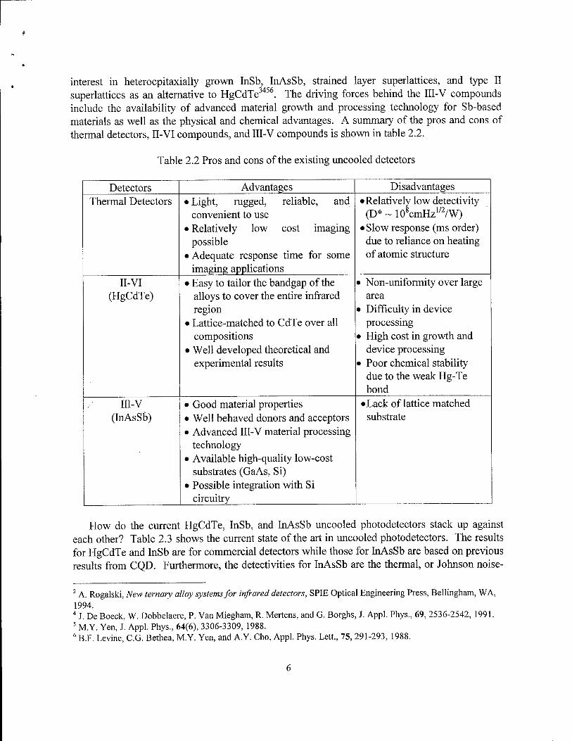
interest in heteroepitaxially grown InSb, InAsSb, strained layer superlattices, and type II superlattices as an alternative to HgCdTe3456. The driving forces behind the III-V compounds include the availability of advanced material growth and processing technology for Sb-based materials as well as the physical and chemical advantages. A summary of the pros and cons of thermal detectors, II-VI compounds, and III-V compounds is shown in table 2.2.
Table 2.2 Pros and cons of the existing uncooled detectors
Detectors Advantages Disadvantages Thermal Detectors • Light, rugged, reliable, and
convenient to use • Relatively low cost imaging
possible • Adequate response time for some
imaging applications
•Relatively low detectivity (D* ~ 108cmHz1/2/W)
• Slow response (ms order) due to reliance on heating of atomic structure
II-VI (HgCdTe)
• Easy to tailor the bandgap of the alloys to cover the entire infrared region
• Lattice-matched to CdTe over all compositions
• Well developed theoretical and experimental results
• Non-uniformity over large area
• Difficulty in device processing
• High cost in growth and device processing
• Poor chemical stability due to the weak Hg-Te bond
III-V (InAsSb)
• Good material properties • Well behaved donors and acceptors • Advanced III-V material processing
technology • Available high-quality low-cost
substrates (GaAs, Si) • Possible integration with Si
circuitry
•Lack of lattice matched substrate
How do the current HgCdTe, InSb, and InAsSb uncooled photodetectors stack up against each other? Table 2.3 shows the current state of the art in uncooled photodetectors. The results for HgCdTe and InSb are for commercial detectors while those for InAsSb are based on previous results from CQD. Furthermore, the detectivities for InAsSb are the thermal, or Johnson noise-
3 A. Rogalski, New ternary alloy systems for infrared detectors, SPIE Optical Engineering Press, Bellingham, WA, 1994. 4 J. De Boeck, W. Dobbelaere, P. Van Miegham, R. Mertens, and G. Borghs, J. Appl. Phys, 69, 2536-2542, 1991. 5 M.Y. Yen, J. Appl. Phys., 64(6), 3306-3309, 1988. 6 B.F. Levine, CG. Bethea, M.Y. Yen, and AY. Cho, Appl. Phys. Lett., 75, 291-293, 1988.

limited detectivities while the detectivities for the commercial detectors are as reported by the manufacturers of those devices.
The reason for this discrepancy is because the InAsSb has a low resistance. This is true for all detectors with narrow band gaps at room temperature. The noise floor of the spectrum analyzer used by CQD is approximately 5nV/Hz1/2. For a typical detector resistance of 6 Q, the noise current would need to be at least at least 1 nA/Hz1/2 for the noise voltage to be measured. For Johnson noise limited detectors, the noise current is
4kBTAf . /TT m L = B J nA/Hz (2.2)
Table 2.3 State of the art in uncooled photodetectors
X (urn) HgCdTe (cmHz1/2/W) InSb (cmHz1/2/W) InAsSb (cmHz1/2/W) 5 6 7 8
5xl08
3xl08
2x10s
2xl08
2xl08
2xl08 4.5xl08
3xl08
.1/2 .1/2 For R0 = 6 Q, in = 0.0526 nA/Hz"z, which is much smaller than the 1 nA/Hz required. The current is so small that the spectrum analyzer will not register a noise voltage. This is a limitation that needs to be overcome to be able to fully assess the performance of the CQD detectors. It will be shown in chapter 3 that a full detector has been developed including the packaging, the immersion lens, and the preamplifier circuit. For these detectors, we are able to measure the noise and calculate the specific detectivity rather than the Johnson noise-limited detectivity.
2.4 A Review of the InAsSb Material System
A brief review of the InAsSb material system is required at this point. This section will explain what composition of InAsSb was chosen and why. This should clarify several issues regarding the construction of the devices.
Early data had suggested that InAsSb could be longer than 12.5 um at near room temperature, which may be due to structural ordering7. However, the exact mechanism has not been determined yet. The equation for bandgap versus composition and temperature for the InAsSb material system is
7 K.Y. Ma and G.B Stringfellow, Appl. Phys. Lett., 54, 1154-1156, 1989.

E Ax,T)= 0.235- -4T2 3.4xio;4r
210+r ■0.524x + 0.70x2 +3.4xl0"4r(x-x2) (2.3)
o
where x is the percent composition of As in the ternary compound . At room temperature (300 K) equation (2.3) becomes
E,(x)= 0.598x2 -0.422x + 0.175 (2.4)
The minimum bandgap occurs at a composition of x=0.35. The cutoff wavelength versus composition for InAsSb at 300 K is shown in figure 2.3. The bandgap corresponding to 8 (am is 0.155 eV.
InAsSb Cutoff Wavelength vs Composition at 300K -14 |—,—,—,—,—i—i—,—r
I
> 93
0 InAs
0.2 0.4 0.6
Composition
0.8 InSb
Figure 2.3The InAsSb cutoff wavelengths versus composition at 300K
From the figure, it is apparent that there are two possible compositions of InAsSb that have a cutoff wavelength equal to 8 jam. One composition is As-rich, InAso.66Sbo.34 and one composition is Sb-rich, InAso.06Sbo.94. Based on previous work, the Sb-rich InAso.06Sbo.94 composition was chosen as the active layer material. There are two reasons for this choice. First, the photoresponse for the Sb-rich materials is higher. The photoresponse is higher primarily due to the higher electron mobility in the Sb-rich material. Furthermore, the material quality is much better in the Sb-rich materials than the As-rich materials under MBE growth conditions. Also, the miscibility gap plays a role in the As-rich region and segregation will occur resulting in poor material quality.
1 A. Rogalski, Infrared Photon Detectors, SPIE Optical Engineering Press, Bellingham, WA, 1995.

Secondly, CQD's previous experience with Sb-based materials on GaAs substrates made the Sb-rich material the first choice. This is because the As composition is only 6% so the thin film growth conditions and processing techniques used for InSb should work well here reducing the overall development time for the 5-8 urn photodetectors. The major drawback to using Sb-rich InAsooeSbo.94 is that the lattice mismatch between this material and the GaAs substrate is much larger than the mismatch of the GaAs substrate with the As-rich InAsSb. The extent of this mismatch is evident in the following figure. The lattice constant for InAso.06Sbo.94 is 6.452 A.
The lattice mismatch is 13.2% for the Sb-rich InAso.oeSbo.94. Once the choice of the InAsSb composition has been settled a barrier material is needed for the cladding layer. According to figure 2.4, there are two possible barrier materials for InAs0.o6Sb0.94 that are lattice matched. The two candidates are AllnSb and GalnSb. The energy levels have been calculated for the conduction band and valence band versus lattice constant for InAsSb, AllnSb, and GalnSb. Figure 2.5 shows the results of this calculation.
3.0
2.5
2.0
1.5
1.0
0.5
0.0
-, 1 1 1 1 ■ r
GaP
• Direct band
i Indirect band
InSb ■
5.2 5.4 5.6 5.8 6.0 6.2 6.4
Lattice Constant (A)
6.6
Figure 2.4 Bandgap versus lattice constant for several material systems

>
> _i
0) c
LU
6.2 6.3 6.4
Lattice Constant (A)
Figure 2.5 Energy level versus lattice constant for InAsSb, AllnSb, and GalnSb9
AllnSb has three major advantages over GalnSb. The first is that the carrier confinement would be better because of the larger bandgap at the corresponding composition. The second advantage becomes apparent in figure 2.6. AllnSb has a type I band alignment with InAsSb. This would provide confinement of both electrons and holes in both directions. On the other hand, GalnSb forms a type II band alignment with InAsSb. The effective bandgap of the two layers is reduced to that below the band gaps of either InAsSb or GalnSb. There is no confinement of holes in either direction due to the type II band alignment. The final advantage of AllnSb is technology related. The n-type dopant Si does not dope the GalnSb n-type but rather p-type. Thus, there cannot be an n-type contact for layers with GalnSb. AllnSb can be easily doped p-type or n-type. The composition of the AllnSb was determined using the Picogiga™ program. This composition is Alo.07Ino.93Sb under the lattice matching constraint. The bandgap for this material is 0.292 eV.
9 J.D. Kim, Investigation of InAsSb material system for long-wavelength infrared photodetector applications, Ph.D. Thesis, Northwestern University, 1999.
10

CB
CB
VB
CB
VB
VB
GalnSb
AllnSb InAsSb
Figure 2.6 Band alignments of AllnSb and GalnSb with InAsSb
In comparison to HgCdTe, InAsSb exhibits the inherent advantages of high stability, well- behaved donor and acceptor impurities, high mobility, and availability of low cost and high quality substrates such as GaAs. These characteristics show promise for long-wavelength IR (LWIR) InAsSb photodetectors operating at room temperature. However, InAsSb photodetectors are limited at high temperatures due to the strong thermal generation and recombination of charge carriers.
Table 2.4 Detectivity comparisons of HgCdTe, InSb, and InAsSb at 300K 10
X (um) HgCdTe (cmHz1/2/W) InSb (cmHz1/2/W) InAsSb (cmHz1/2/W)
5 6 7 8
2x10y
7xl08
4x10⁸
2xl08
7x10⁸
7xl08
4x10⁸
2xl09
7xl08
4xl08
2xl08
Several solutions have been proposed to suppress the noise due to Auger recombination . These include the optimization of the detector structure by controlling the composition, doping level, and thickness to enhance the quantum efficiency and improve the efficiency of carrier extraction during the non-equilibrium mode of operation. A comparison of the theoretical performance of uncooled photodetectors operating at wavelengths between five and eight microns is shown in table 2.4. These values were procured from the literature.
10 E. Michel, Sb-based materials for infrared photodetectors: growth, characterization, fabrication, and analysis, Ph.D. Thesis, Northwestern University, 1998. 11 T. Ashley and C.T. Elliott, Electronic Letters, 21,451-452, 1985.
11

103 102 101
£ ■4—»
ri ii ■ i i |ii
No/Ni
100 101 102
1 " ""I—
103
lnASO.06Sb0.94
Po/Ni
m5
10-14
1 9 Figure 2.7 Calculated minority carrier lifetime versus active layer doping level
One way to suppress the Auger recombination mechanism is to determine the optimum doping for the active layer. Figure 2.7 shows the calculated minority carrier lifetime versus the doping level. The Auger 1 and Auger 7 recombination processes are taken into consideration. Auger 1, or CHCC, is dependent on a high electron concentration while the Auger 7, or CHLH, is dependent on a large hole concentration as evidenced by the graph. The radiative lifetime is plotted as a reference. The optimum doping level was determined to be p-type with a concentration of ~3ni5 or 2xl017 cm"3 for the ternary under consideration.
12 J.D. Kim, Investigation oflnAsSb material system for long-wavelength infrared photodetector applications, Ph.D. Thesis, Northwestern University, 1999.
12

Chapter 3 Growth and Characterization All material under this contract was grown using a Varian/Intevac (Applied EPI) Modular Gen II solid source molecular beam epitaxy (SSMBE) reactor. In-situ monitoring of the material growth was achieved using reflection high-energy electron diffraction (RHEED). Material growth was done primarily on GaAs. However, some growths were done on InSb to get a comparison to better quality material given that InSb is nearly lattice-matched to the InAsSb.
All material growths were characterized structurally, electrically, and optically. Structural characterization was done using a five-crystal x-ray diffraction system for crystal quality, a scanning electron microscopy system for thickness and interface quality, and, recently, an atomic force microscopy system for surface quality on an atomic scale. Electrical characterization was done via Van der Pauw patterned Hall measurements. From this, the Hall mobility, carrier concentration, and sheet resistivities were determined. Optical measurements were performed using photoluminescence. The external quantum efficiency of the InAsSb layers was measured using transmission measurements to calculate the absorption coefficient.
3.1 Thin Film Growth
InAsSb and AllnSb layers were grown on (100) GaAs and (100) InSb substrates by SSMBE using uncracked elemental sources. The V/III incorporation rate was set to -1.2/1 using RHEED calibrations. The substrate temperature was monitored using an IR pyrometer calibrated to the centered 4x4 to the asymmetric 1x3 RHEED transition temperature of InSb, ~390°C. The techniques for optimizing growth conditions for heteroepitaxial InSb, which is the foundation upon which the growth of these ternary materials is built, are described in the literature.
The growth conditions for the ternary derivatives of InSb are based on the growth of InSb itself. The basic procedure that turned out to also be the optimal conditions for growth in the SSMBE reactor was to increase either the group III or group V flux, i.e. In or Sb, to accommodate the added element whether it be Al or As. For example, in the growth of InAsSb, the In flux is increased to accommodate the added As. This is necessary in order to create lattice sites for the As adatoms. Otherwise, As will not incorporate into the growth in significant quantities. Furthermore, it was found that the growth temperature was slightly higher for optimal growth. The V/III ratio is still -1.2/1 for the ternary growths at a growth temperature of ~400°C. Under these growth conditions, high quality material has been obtained.
3.2 Material Characterization
After optimization of the material growth, the InAsSb, AllnSb, and GalnSb epilayers were
13
characterized. Typical values for the InAsSb epilayers include x-ray FWHMs less than 400 arcseconds and electron mobilities greater than 40,000 cm2/Vs at 300K. Typical values for the AllnSb and GalnSb epilayers include x-ray FWHMs less than 400 arcseconds and PL FWHMs less than 30 meV at 77 K.
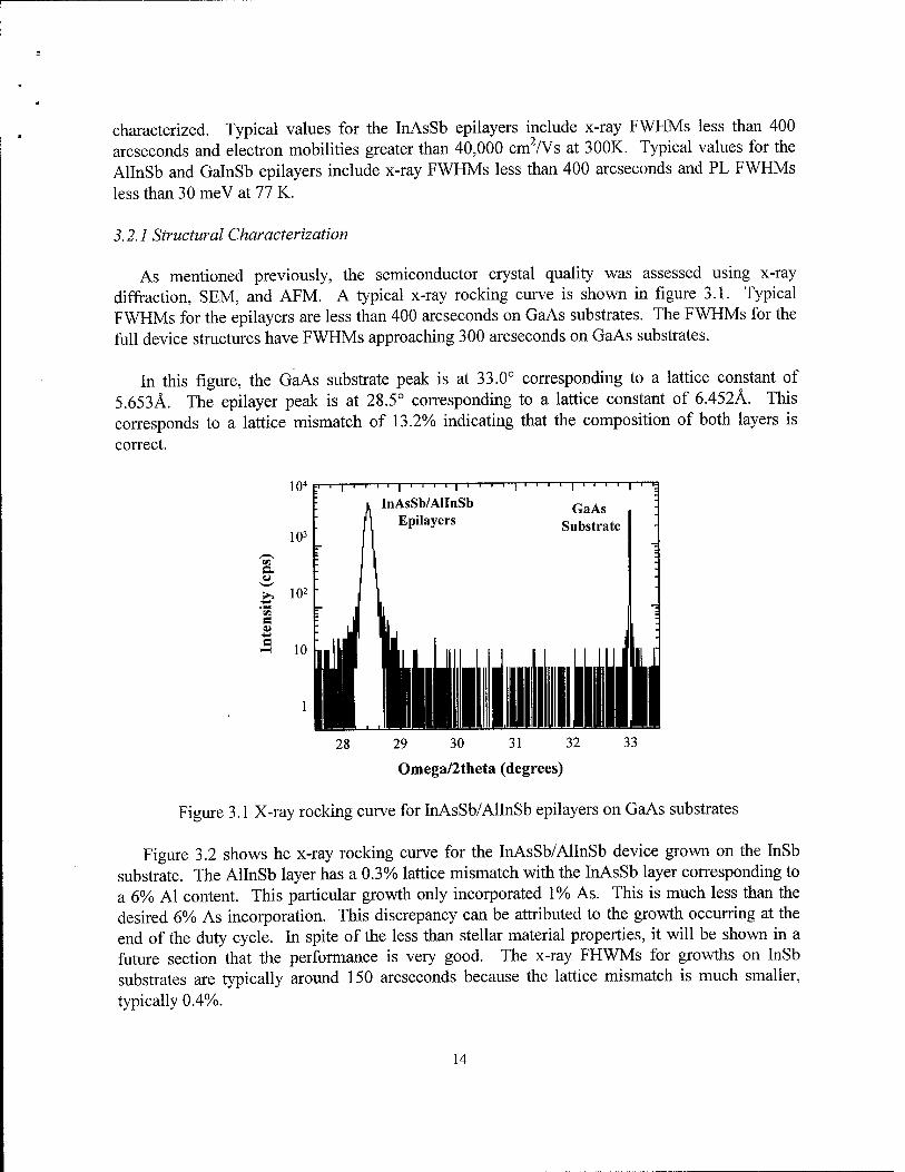
3.2.1 Structural Characterization
As mentioned previously, the semiconductor crystal quality was assessed using x-ray diffraction, SEM, and AFM. A typical x-ray rocking curve is shown in figure 3.1. Typical FWHMs for the epilayers are less than 400 arcseconds on GaAs substrates. The FWHMs for the full device structures have FWHMs approaching 300 arcseconds on GaAs substrates.
In this figure, the GaAs substrate peak is at 33.0° corresponding to a lattice constant of 5.653Ä. The epilayer peak is at 28.5° corresponding to a lattice constant of 6.452Ä. This corresponds to a lattice mismatch of 13.2% indicating that the composition of both layers is correct.
29 30 31 32
Omega/2theta (degrees)
Figure 3.1 X-ray rocking curve for InAsSb/AlInSb epilayers on GaAs substrates
Figure 3.2 shows he x-ray rocking curve for the InAsSb/AlInSb device grown on the InSb substrate. The AllnSb layer has a 0.3% lattice mismatch with the InAsSb layer corresponding to a 6% Al content. This particular growth only incorporated 1% As. This is much less than the desired 6% As incorporation. This discrepancy can be attributed to the growth occurring at the end of the duty cycle. In spite of the less than stellar material properties, it will be shown in a future section that the performance is very good. The x-ray FHWMs for growths on InSb substrates are typically around 150 arcseconds because the lattice mismatch is much smaller, typically 0.4%.
14

10
27
InAsSb Layer,
AllnSb Layers
28.2 28.4 2B.6
Omega / 2Theta (degrees)
Figure 3.2 X-ray rocking curve for the DH structure grown on InSb substrate
Although the composition and the structure seem fine, what does the actual surface look like? SEM reveals that the structure is microscopically smooth which should be expected since the surface looks mirror-like to the naked eye. However, AFM reveals that the surface is not atomically smooth for the GaAs substrates while it is nearly atomically smooth for the InSb substrates. Figure 3.3 shows a three dimensional picture of the surface for the growth on GaAs substrate.
'' M.
4sr
Digital InstrUMents NanoScope •t Scan size 10.00 JJM
,.'■'. Scan rate 1.001 Hz -.. , NuMber of sanples 256 sSÄ'Äi iMage Data Height /ft-XrVf-, Data scale 10.00 nn
'•h,,jf:'jS ri0 ' ■■■•■■^W'U -W'^'^"'' 9i r vie"an!"8 ^.titf-^i ÄvfT Vi^K^': JjS 1 .£. light angle
1 '!■»"' ft:' **&«- .^f
v, ..
2
4
yTf J>^f" f<' / / \
■;."? fe.'isw?*""-4' .-.' X 1 /
G
8 , ' / X 2.000 UM/di« ° de9
/ 2 10.000 nM/diw
m snbel092.000
Figure 3.3 AFM image of the double heterostructure on the GaAs substrate
The vertical scale is 10 nm. The root-mean-square (rms) roughness of the surface is 1.3 nm or
15

the thickness of several atomic layers. This is not surprising due to the lattice mismatch between the thin film and the substrate. It is well known that in lattice mismatched heteroepitaxy the thin film growth switches from layer growth to island growth once a critical thickness is exceeded. This is because the island growth minimizes the surface free energy as compared to layer growth.
Figure 3.4 shows the AFM image for the growth of the double heterostructure on the InSb substrate. The rms surface roughness is typically around 0.4 nm. This is slightly larger than an atomic layer, which is to be expected due to the minimization of the free energy as explained in the previous paragraph. The surface is much smoother due to the smaller lattice mismatch.
Figure 3.4 AFM image of the DH structure on InSb substrate
It should be kept in mind that techniques, such as graded layers or superlattices, could be used to remove dislocations and defects between two lattice-mismatched materials. Up to this point, no attempt has been made to reduce dislocations because it has been mandated that the devices be as cheap as possible for the proximity fuze application. In the future, such techniques will be utilized to improve the material quality.
3.2.2 Quantum Efficiency
The quantum efficiency is a measure of how many electron-hole pairs (EHPs) are generated per incident photon. Ideally, one EHP should be generated per incident photon. However, due to reasons such as crystal imperfections and the reflection of photons at the sample surface, the quantum efficiency is less than one. Thus, the quantum efficiency is a reflection of the quality of the device. In order to optimize the device, the quantum efficiency needs to be optimized.
16

In order to determine the quantum efficiency, the absorption coefficient for the material must be determined. The absorption coefficient of the active layer was determined through successive etching and transmission measurements of the device. Figure 3.5 shows the resulting transmittance spectra for the successive etches. Note the Fabry-Perot oscillations in the curves. This is an artifact of the FTIR spectrometer setup.
Transmittance Spectra 100
10
1 ■— ■ 1 1 ' 1 ' 1
: i>;llß^\ ill // \ / / / / :/ / / T = 300K
5 6 7
Wavelength (|im)
- No Etch
- • 0.5 \xm Etch
--■ 1.0 Jim Etch
• 1.5 \im Etch
- 2.0 |im Etch
3 um InAsSb
3(iin ii+ MlnSli
GaAs Substrate
Figure 3.5 Transmission spectra after successive etches of the InAsSb active layer
The figure shows that as the wavelength of the light increases the absorption decreases. The quantum efficiency is computed at 7 jam because the peak response of the detectors occurs here. An Arrhenius plot of the transmittance versus layer thickness at 7 urn gives the absorption coefficient. In this case, the absorption coefficient is 1800 cm"1. Figure 3.6 shows the Arrhenius plot.
17

Transmittance at X = 7 (im 100
^5
Ü C
■ 1 > 1 ■ r - ■ i
T = 300K
\« ■
• V
•\
i.i.i i i.i.
0.0 0.5 1.0 1.5 2.0 2.5 3.0 3.5
Layer Thickness (jim)
Figure 3.6 Arrhenius plot of the transmittance versus layer thickness.
The quantum efficiency is given by
17^(1-*) 1-e"
1-Re" (3.1)
where a is the absorption coefficient, t is the thickness of the material, and R is the reflectivity of the material. The reflectivity is determined by
R = n-\
n + \ (3.2)
where n is the refractive index of the semiconductor material. InAsSb has a refractive index of 3.9. This gives a reflectivity of 0.35. Equation (3.1) gives a value of 0.35 for the experimental quantum efficiency. 1

Chapter 4 Device Analysis This chapter is the culmination of the research performed over the past three years on
InAsSb. Most of the work has been primarily on GaAs substrate for the proximity fuze application. First, simple InAsSb p-i-n photodiodes were investigated to see if the application requirements could be met. Next, heterostructure devices utilizing larger bandgap barrier materials were investigated. Both single and double heterostructures yielded an improvement in performance. Recently, work has been done on InAsSb and InSb on InSb substrates to investigate the potential of the devices with reduced dislocation densities.
Once the material was optimized, several devices were investigated for the proximity fuze application. A step-by-step study of different p-i-n devices was implemented. Each device had one change from the previous device. First, the simplest of photodiodes was investigated, the InAsSb homojunction. The second step was to determine the best barrier material that can be used. The two choices were GalnSb and AllnSb. Ultimately, AllnSb was chosen as the barrier materials for the heterostructure photodiodes as explained previously in section 2.4.
Next, the homojunction performance on an AllnSb buffer layer was investigated. Next, the InAsSb/AlInSb single heterostructure photodiode was investigated. This utilized a barrier for one carrier. The final step was to investigate the InAsSb/AlInSb double heterostructure. This device structure utilizes the barriers for both electrons and holes and should have the highest efficiency and photoresponse of the studied photodiodes. In the end, these devices have the highest performance of any devices that were studied under this contract. Furthermore, these devices easily meet the detection requirements for the proximity fuze application as shown in the attached report from AAEC.
A clarification needs to be made with regard to the measurements and calculations done for these devices. Given that the room temperature signal in general is weak primarily because of the Auger recombination mechanisms, it has been impossible to obtain zero bias spectral responses for most of the devices. Furthermore, the detectors' noises cannot be measured with the spectrum analyzer because the device resistances are low. The noise is well below the floor of the spectrum analyzer. Thus, the only way to calculate the detectivity for these devices is to assume that the Johnson noise limit applies for the reverse bias regime as well as zero bias. In general, this is not a correct assumption because the generation-recombination (G-R) noise is comparable to and dominates the Johnson noise under reverse bias conditions. With the exception of the double heterostructure devices, the detectivities are to be viewed as a measuring stick for progress rather than an absolute performance measurement.
Furthermore, the detectivity requirements calculated by AAEC were derived from the system
19

SNR for the proximity fuze application giving the so-called system detectivity. Hence, using an optical immersion lens, anti-reflective coatings, and surface passivation can enhance the actual detectivity of the bare detectors. Additionally, the detectors were analyzed in a system that mimics the proximity fuze system to give a proof of concept, that the InAsSb photodetectors can meet the performance requirements of the proximity fuze application.
The structures were processed into devices using standard photolithography techniques. The mesas were defined using photoresist and etched using a lactic acid and nitric acid combination, a common wet etchant. A liftoff mask was used to lay the top and bottom contacts onto the devices. The final devices measured 400x400 (am with a 150x150 (am top contact and a 150x300 urn bottom contact. During measurements the detectors were topside illuminated.
4.1 InAsSb Homojunction Photodiodes
The first device structure investigated was the InAsSb homojunction photodiode grown directly on the GaAs substrate with a thin p-type InSb buffer layer. Initially, the device structure was an n+/7t/p+ structure as shown in figure 4.1. This structure consists of a 3-um InAsSb active layer surrounded by heavily doped InAsSb contact layers.
Ti-lnAsSb | Wavelength (urn) -'A jpr,
p-InAsSb j£,\- i p-InSb buffer l»yer
GaAs Substrate
GaAs :SüifoSt*a'fe f I \ p InAsSb / n InAsSb
71 - InAsSb
Figure 4.1 InAsSb n+/7i/p+ homojunction structure
This is a standard p-i-n photodetector that has a 71-doped, or lightly p-type doped, active region to enhance the performance of the photodiode by maximizing the carrier lifetime. At room temperature, the limiting factor in the carrier lifetime is the CHCC, or Auger 1, recombination process. By lightly doping the active region, the CHLH, or Auger 7, recombination process becomes more significant at the expense of the Auger 1 recombination process. The maximum carrier lifetime corresponds to the desired doping level.
Figure 4.2 shows the absolute photoresponse resulting from the homojunction photodiodes. The peak response occurs at 6.5 urn with a 50% cutoff wavelength at 7 p.m. The zero bias Johnson noise-limited detectivity is estimated to be 3x10⁶ cmHz1/2/W. Under reverse bias, the detectivity can be increased to 1.5xl08 cmHz1/2/W if we assume that the Johnson noise limit still
20

applies. The photoresponse is low primarily due to the loss of many electrons in the highly dislocated region in the p-type InAsSb layer.
InAsSb/InSb n- % -p Spectral Response
4 5 6 7 Wavelength (\xm)
Figure 4.2 InAsSb n+/7r/p+ spectral response
OK
1.2
1
0.8
0.6
0.4
0.2
1 ' ' ! ' ' Undopi d
1 ;
.
r
. / ■
■
. i. ...i—i— * ■ i ■ ■ ■ L^G>
210L 4 10J 610" 10" Be Doping Level (cm )
1 10"
Figure 4.3 Relative responses for various active layer Be concentrations 13
It should be noted here that none of the following devices have rc-doped active regions. By comparing various doped active layer photodiodes with the undoped active layer photodiode and comparing the relative response as shown in figure 4.3, it was determined that the undoped active region gave a higher photoresponse than the 7t-doped active region. As mentioned previously, the optimum response should occur at ~3nj. The experiment matches the theory nearly perfectly. The intrinsic carrier concentration for InAsSb with 6% As is ~5xl016 cm-3. The maximum response is highest in the device with ~2xl 017 cm"3 p-type doping. But why does the undoped
13 E. Michel, Sb-based materials for infrared photodetectors: growth, characterization, fabrication, and analysis, Ph.D. Thesis, Northwestern University, 1998.
21

sample have a higher photoresponse than the 71-doped sample. The high number of SRH recombination traps counters the effect of lightly doping the active region p-type. Therefore, the devices with the intrinsic active regions had the higher photoresponse.
n+-InAsSb
nt-InAsSb
AllnSb buffer layer ■/;
GaAs Substrate -InAsSb
InAsSb
Figure 4.4 InAsSb homojunction on an AllnSb buffer layer
Due to the large lattice mismatch between the device structure and the GaAs substrate (13.2%), there is a highly dislocated layer at the interface. These dislocations will propagate through the sample until they join together or reach the top of the sample. It is imperative that the electrons are kept away from this highly dislocated layer. A lattice matched AllnSb buffer layer was grown between the device structure and the GaAs substrate as shown in figure 4.4. The purpose of this layer is to keep the electrons away from the highly dislocated region; thus, increasing the carrier lifetime. Essentially, the band offset will provide a barrier to the electrons.
The photoresponse for the InAsSb homojunction photodiode on an AllnSb buffer layer is shown in figure 4.5. As expected, the presence of the wide bandgap buffer layer improved the performance of the device significantly. However, the barrier material added a photoresponse at the shorter wavelengths. This is attributed to part of the electric field dropping across the AllnSb because it has a much larger resistance than the InAsSb. Thus, the efficiency of the buffer layer is improved greatly under reverse bias compared to the active layer.
InAsSb/AIInSb Photodiode Spectral Response
< E
a o a.
9 ja
si <
64 _ II 1 1 1 1 1 1 1—1 1"" l 1 l ■ 1 l • 1 1 l ■ L_
56 ~~imi
48 ' 1 ^BM^VIL »J 1 '■ 40 "wL -;
32 - Ill -_
24 - ySi -_
16 r \ '.
8 Vlii A '■ n :....,....,... y\n. wu/viAAurtlr^
5 6 7 Wavelength (fim)
22

Figure 4.5 Spectral response of the InAsSb homojunction on the AllnSb buffer layer
The peak wavelength shifts to a shorter wavelength. However, there is a significant improvement in the photoresponse and detectivity of the device. In this case, the peak wavelength has shifted down to 4.2 um. At 6.5 urn, Johnson noise-limited detectivity is estimated to be lxlO7 cmHz1/2/W at zero bias. The detectivity can be increased to lxl08
cmHzI/2/W under reverse bias mode assuming the device is Johnson noise-limited.
4.2 InAsSb/AlInSb Single Heterostructure Photodiodes
Given the performance of the InAsSb homojunction and its subsequent improvement in performance with the addition of the AllnSb buffer layer, InAsSb/AllnSb single heterostructure devices were the logical next step. This device structure consisted of a 3 urn active region with a p+-InAsSb top contact layer and a n+-AHnSb bottom contact layer. The AllnSb layer will create a barrier to the holes. Due to charge neutrality requirements in the device, the electron lifetime will be enhanced allowing more of them to reach the contact and register a signal on the external circuitry. This device structure and the corresponding band alignment are shown in figure 4.6.
i-InAsSb /ß
' n'-AUnSb '''^
GaAs Substrate
IT -AllnSb / pMnAsSb
i-InAsSb
Figure 4.6 InAsSb/AllnSb single heterostructure photodiode
23

InAsSb/AlInSb SH Spectral Response
4 5 6 7 Wavelength (fim)
Figure 4.7 InAsSb/AlInSb single heterostructure spectral response
Due to the addition of the AllnSb barrier layer, the peak response is enhanced significantly at short wavelength compared to the long wavelength response. This is attributed to most of the reverse bias falling across the higher resistant AllnSb layer. The spectral response is shown in figure 4.7. The Johnson noise-limited detectivity is estimated to be lxlO7 cmHz1/2/W at zero bias at 6.5 urn. The detectivity can be increased to 3x10⁸ cmHz1/2/W under the Johnson noise limit while operating in reverse bias mode.
The single heterostructure photodiode showed an unusually strong response at shorter wavelengths as explained earlier. This device was measured at liquid nitrogen temperature (77K) to get a sense of the two-color detection scheme. The two-color spectral response is shown below in figure 4.8. At zero bias, the response cuts off at nearly 6 urn while at 2V reverse bias the response cuts off at 3.4 um. Thus, a two-color detection scheme exists with the InAsSb/AlInSb single heterostructure depending upon the bias mode. It should be kept in mind that this detector is optimized for operation at room temperature.
24

2.5 109
2 109
t 1.5 109
Q
2-color Spectral Response i—i—i—i—i—i—i—i—I—i—i—i—i—|—l—i—i—l—f
2V Bias
OV Bias
4 5 6 Wavelength (um)
Figure 4.8 InAsSb/AlInSb single heterostructure two-color spectral response
While the single heterostructure provided a significant improvement in performance, its behavior relative to the biasing scheme is not acceptable for the proximity fuze application. To avoid the wavelength shift due to biasing the double heterostructure device design was employed. This device provides two advantages over the single heterostructure that will be seen the next section. Given that the double heterostructure photodiodes succeed in meeting the contract technical objectives, the next section is dedicated to the analysis of these devices.
4.3 InAsSb/AlInSb Double Heterostructure Photodiodes
There are two advantages that double heterostructure photodiodes offer over the previously investigated devices. First, there is a barrier for both holes and electrons. Because carriers are confined in one direction, this enhances the quantum efficiency of the device. Furthermore, the double heterostructure design provides an inherent way to enhance the carrier lifetime by reducing the Auger recombination rate.
3.0 \i»Jt i-InAsSb ^#1^
Ä|i||iJ|J||pj|lpi||
GaAs Substrate
M n*-AUnSb / p+-AHnSb
i-InAsSb
Figure 4.9 InAsSb double heterostructure and its band alignment
25

The p+-AHnSb barrier layer serves as a sink for the minority carriers (holes) in the active region. The carriers move primarily by diffusion and reverse biasing the diode will enhance this. This minority carrier extraction results in the reduction of minority carriers because the holes are not injected back into the active layer. The charge neutrality requirement leads to a reduction in the majority carrier concentration (electrons) in the active layer. This lead to a reduction in the Auger recombination rate because the Auger process is exponentially dependent on the carrier concentration. The effectiveness of the carrier extraction is technologically limited by the background carrier concentration .
4.3.1 Double Heterostructure Devices on GaAs Substrates
These photodiodes consisted of p+-AHnSb/InAsSb/n+-AlInSb double heterostructures on (100) GaAs substrates. The n+-AHnSb layer has a doping level of approximately 1018 cm"3 to provide a barrier layer that keeps electrons away from the highly dislocated AlInSb/GaAs interface, thus increasing the carrier lifetime. The InAsSb active region is 3 urn thick with an intrinsic carrier concentration of ~5xl 016 cm"3. The p+-AHnSb has doping level of 1018 cm"3 to provide a barrier to the holes. The device structure and its band alignment are shown in figure 4.9.
InAsSb photodiodes were grown on GaAs substrates for the proximity fuze application. In spite of the lattice mismatch these photodiodes exceeded the project goals when operated under reverse bias. The performance of the detectors is evaluated in this section.
The differential resistance of the device at room temperature is shown in figure 4.10. The graph displays typical diode behavior. The differential resistance increases as the reverse bias voltage increases because the potential barrier increases. On the other hand, the differential resistance decreases as the forward bias is increased because the potential barrier decreases. For the photodiodes, the desired operating regime is the reverse bias mode because of the higher responsivity of the device in that regime. Of course, there is a limit on how large a reverse bias can be applied. At higher biases, the generation-recombination noise becomes comparable to the thermal noise; thus, reducing the actual detectivity of the device.
To determine the absolute photoresponse, the relative response was measured using a FTIR spectrometer, and the absolute responsivity of the detector was measured using a chopped signal from a calibrated blackbody source at 800°C.
14 C.T. Elliot, Semicond. Sei. Technol., 5, S30-S37, 1990.
26

-0.4 -0.3 -0.2 -0.1 0.0 0.1 0.2 0.3 0.4 Bias (Volts)
Figure 4.10 Differential resistance versus applied bias
The spectral response of the sample was measured at room temperature at zero bias with a FTIR spectrometer. The spectral response is shown in figure 4.11. The peak response occurs at approximately 6.5 urn. All devices exhibited a 50% cutoff wavelength of 7.5 urn. These double heterostructure devices were the first devices that the spectral response could be measured at both zero bias and reverse bias. This is important given the shift in peak wavelength has occurred in some of the other devices. In this case, there is no shift in the peak wavelength. The only change is the enhanced response of the signal at all wavelengths compared to the zero bias case. In fact, the effect of the biasing increased the response at the peak wavelength more than at any other wavelength. This would be expected given the device design.
Because minority carrier extraction reduces the majority carrier level to maintain charge neutrality in the active layer, the effective resistance of the active layer increases beyond that of the AllnSb layers. Thus, most of the applied voltage bias will drop across the active region enhancing its photoresponse more than the barrier layers.
27

5 6 7 Wavelength (um)
10
Figure 4.11 Photodiode spectral responsivity
The Johnson noise limited detectivity of the devices at room temperature is calculated using15
£>* = R,^W (4.1)
where A = 1.6xl0~3 cm2 is the detector area. Since the differential resistance varies from four to nine ohms, there is a slight increase in the detectivity relative to the responsivity of the device. This results from the decrease in the theoretical thermal noise. It should be noted that the U.S. Army Research Laboratory in Adelphi, MD has confirmed these results16. The measurement error between the two setups is 20%. However, it is not unusual for the detector response to vary two or three times between measurement setups. There are just too many variables that need to be taken into account to have identical setups.
The peak responsivity is 90 mA/W with a corresponding Johnson noise-limited detectivity of 5xl07 cmHzI/2/W at 6.5 urn under zero bias. The peak responsivity increases to 300 mA/W
Q I/O
under reverse bias. The detectivity increases to 5x10 cmHz /W under reverse bias assuming the Johnson noise limit still applies17. The double heterostructure photodiode is the only detector that meets the requirements for the proximity fuze application and detects at the correct wavelengths.
15 J.D. Vincent, Fundamentals of Infrared Detector Operation and Testing, Wiley, New York, 1990. 16 Private communication with Steve Kennerly at Army Research Laboratory 17 J. S. Wojkowski, H. Mohseni, J.D. Kim, and M. Razeghi, SPIE Proceedings: Photodetectors: Materials and Devices IV, 3629, 357-363, 1999.
28

Since the proximity fuze application must sample at a relatively high frequency, -20 kHz, the frequency responsivity of the device has been measured. However, due to the limitations of CQD's chopper speed, the measurement is only up to 4 kHz as shown in figure 4.12. As expected the device shows no dependence on the frequency up to that point.
100 1000 Frequency (Hz)
0000
Figure 4.12 Frequency response of the photodiode
InAsSb/AlInSb double heterostructures grown on GaAs substrates have been demonstrated to meet the minimum requirements for the proximity fuze application. In collaboration with AAEC, the detectors have been mounted into a detector package and tested with a prototype readout circuitry designed to work with low impedance devices. These results will be presented in a separate report submitted by AAEC.
4.3.2 InAsSb Photodiodes on InSb Substrates
Double heterostructure InAsSb/AlInSb devices were grown on InSb substrate to take advantage of the smaller lattice mismatches leading to better crystalline quality and better device performance particularly in the reverse bias regime. In fact, the performance is nearly an order of magnitude higher due to the reduction in the number of dislocations for the double heterostructure photodiode. The lattice mismatch in this case is only 0.4%.
The IV curve and the corresponding differential resistance are shown in figure 4.13 below. Again, the photodetector shows typical diode behavior. The current increases and the resistance decreases as the forward bias is increased. On the other hand, as the reverse bias is increased the current decreases and the resistance increases until saturation is achieved. In this case, the rectification is much more significant than with the devices grown on GaAs substrates. The
29

primary reason for this is the reduction of the dislocations and defects that leads to a reduction in the number of SRH recombination sites. Thus, carrier extraction is more effective leading to a significant improvement in performance.
0.08
0.06
o 0.04
'S
U 0.02 U
0.00
-0.02
-0.6 -0.4 -0.2 0.0 Bias Voltage (V)
0.2
80
60 §
O
Figure 4.13 IV Curve and differential resistance response
In this case, the resistance saturates at 60 Q instead of 8 Q like the devices on the GaAs substrates. Furthermore, the device performance saturates much quicker than GaAs substrate- based devices indicating better carrier extraction.
The spectral response for this structure under zero bias is shown in figure 4.14. Since the device structure-itself is the same as the one described in the previous section, the photoresponse is essentially the same. The main reason that this photoresponse looks smoother is primarily due to the larger signal that is generated by this detector. The FTIR does not have to average a large number of times in order to remove the background noise. Once again, note the Fabry-Perot oscillations in the response that are artifacts of the system.
However, under reverse bias the response at shorter wavelengths increases significantly. This shifts the peak response from 6.5 urn to 3 urn. It is hypothesized that the n+-InSb substrate contributes significantly to the detection process when contact is made to the substrate. This was confirmed when the bottom contact was placed on the n+-AHnSb layer so that the conduction path does not include the substrate.
30

1.0
0.6
0.4 -
£ 0.2 -
0.0
- ' 1 ■""' 1 ' I
T = 300K ^//X
i ' i
No bias f^ \ - i
- \
- \ ■ \ - \ • V - i.i.i 1 1
4 6 Wavelength (urn)
10
Figure 4.14 Spectral response for the DH structure on InSb substrate
The detectivity and responsivity were calculated using the absolute response measurements from the blackbody setup and the relative response measurement from the FTIR setup as discussed previously. Equation 4.1 is used to calculate the detectivity from the responsivity. Both the detectivity and the responsivity are significantly larger for the double heterostructure on the InSb substrate than the devices grown on GaAs substrate. In fact, at a very small reverse bias, -0.1 V, the detectivity improves by an order of magnitude while the responsivity doubles.
The peak responsivity is 210 mA/W with a corresponding Johnson noise-limited detectivity of 2xl08 cmHz1/2/W at 6.5 um under zero bias. The detectivity increases to 3xl09 cmHz1/2/W under reverse bias assuming the Johnson noise limit applies.
To really show that the quality of the material has improved the performance of the device, the external quantum efficiency will be calculated. The formula relating quantum efficiency to the absolute responsivity of the device is
'hc^
1 ) Ä (4.2)
where r\ is the external quantum efficiency, h is Planck's constant, c is the speed of light, q is the electronic charge, Rj is the current responsivity, and X is the peak wavelength. Taking the constants in SI units, A, to be 6.5 (am and 3 jam for 0 V and -0.1 V bias, the quantum efficiency at 0 V and -0.1 V respectively, we get 4.4% and 22% respectively. The application of a Si/SiC^ anti-reflection coating led to a 32% increase in the responsivity, thus improving the quantum efficiencies at 0V bias and -0.1 V bias to 5.8% and 29% respectively. A similar calculation for
31

the devices on GaAs substrate gives 2.1% for 0 V bias and 4.1% for -0.1 V bias. This compares to 3.8% and 38% for 0 V and -0.1 V bias for HgCdTe18.
4.4 Detector Packaging
The results up to now have been for a bare detector. In order to improve the photodiode performance, possible detector packaging has been investigated. Proper packaging would allow a more accurate assessment of the device performance. Improvement of the detector performance could be achieved with optical immersion and the use of a preamplifier to boost the signal. The primary requirement for the package is that it has to have gold contacts. The primary reason is because the lab's wire bonder uses gold wiring to make connections. It is unable to connect the gold wiring to the aluminum contacts. Aside from this, the smaller the detector package is the better. The detector package is shown in figure 4.15. A pen is shown in the background as a reference.
Figure 4.15 Detector package shown with a pen in the background
The detector package is a TO-8 transistor package with an infrared Fresnel lens mounted at the top and a preamplifier mounted at the bottom of the package. A schematic diagram of the interior of the package is shown in figure 4.16. The preamplifier is centered upside-down in the package with the detector placed on top of it. The top of the TO-8 transistor package has been removed. The Fresnel lens is situated in its place.
IS Private communication with Steve Kennedy at Army Research Laboratory
32

Fresnel Lens
Resistor nMDif? ot
Detector
Figure 4.16 A schematic diagram of the TO-8 detector package
A schematic diagram of the external circuit is shown in figure 4.17. This is the circuit used for amplification of the electrical signal under unbiased conditions. The output impedance of the preamplifier is comparable to the output of the detectors (-1-5 Q). This is much less than the input impedance of the readout circuitry (-1-10 kQ). However, the input impedance of the lock- in amplifier is comparable to the output impedance of the detector. Thus, the entire electrical signal is detected. The preamplifier is an ultra-low-noise 0.9-nV/Hz1/2 amplifier with a large bandwidth (10MHz) as specified by the manufacturer Analog Devices. As it turns out, the headers and preamplifier circuits are similar to the ones designed and used by AAEC for the final testing. In this case, the circuit is more complex to allow for the biased mode of operation.
AlOnF B 100 nF C 10 kQ
Input
A =}=B ±B
Jl
Figure 4.17 Schematic diagram of the preamplifier and circuit for the unbiased case 19
19 J. Wojkowski, Uncooled InAsSb infrared photodetectors for the 5-8 jum atmospheric absorption spectrum, M.S Thesis, Northwestern University, 1999.
33

A circuit for measurement under bias is currently being designed. This circuit is a little more complex and requires more circuit elements. Because more circuit elements are required, thin film hybridization is needed. Otherwise, all of the circuit elements will not fit into the detector package. Thin film hybridization is miniaturization of the circuit components onto a thin film with a pre-designed pattern for the metal interconnects.
The preamplifier and the optical immersion provide a marked improvement in the photodiode performance over the bare detector case. The addition of the preamplifier increased the responsivity of the device from 0.6 V/W to 1 kV/W. Optical immersion increases the detectivity of the photodiode from 8xl07 cmHz1/2/W to ~109 cmHz1/2/W.
4.5 Uncooled InAs/GaSb Type II Photovoltaic Detectors
Type II photodetectors offer an inherent advantage over interband detectors because of the spatial separation of electrons and holes. This separation leads to built-in suppression of the Auger recombination mechanism. Although type II detectors are currently being investigated for other uses, an uncooled InAs/GaSb type II photodetector was measured to see what its performance would be compared to the interband detectors. The structure and design have been reported elsewhere20. The zero bias Johnson noise limited detectivity of the type II photodetector was lxlO8 cmHz1/2/W at 7.5 um. The cutoff wavelength is 8 urn. The AAEC report contains the impressive results of this photodetector.
20 H. Mohseni, J. Wojkowski, A. Tahraoui, and M. Razeghi, Proceedings ofSPIE: Photodetectors: Materials and Devices V, SPIE Optical Engineering Press, Bellingham, WA, 2000.
34
Chapter 5 Summary and Future Work Prototype uncooled high-speed InAsSb IR photodetectors have been successfully developed
for the U.S. Navy proximity fuze application. There are several notable technical accomplishments for this contract. High quality lattice-matched ternary materials have been grown successfully on GaAs: InAsSb, AllnSb, and GalnSb (X-ray FWHM < 400 arcsec on GaAs, U300K ~ 40,000 cm2/V-sec, ~ 30 meV PL FWHM). InAsSb homojunction photodiodes have been demonstrated with a RQA product of 1x10" Q-cm and a Johnson noise-limited detectivity of 1.5xl08 cm-Hz1/2/W at a peak wavelength of 6.5 urn under reverse bias. A theoretical investigation of the barrier material systems for the InAsSb photodetectors led to the selection of AllnSb through the calculation of band offsets. The photodetector performance improved using an AllnSb barrier layer. This increased the Johnson noise-limited detectivity to 3><108cm-Hz1/2/W at 6.5 urn under reverse bias.
The first two-color InAsSb/AllnSb photodetectors with a Johnson noise-limited detectivity of 4x108 cm-Hz1/2/W for A, ~ 3 urn and lxl08 cm-Hz1/2/W for A ~ 6.5 um were successfully demonstrated. The first double heterostructure InAsSb detectors using AllnSb barriers with an extended cutoff wavelength (8 urn) were successfully demonstrated. The Johnson noise-limited detectivity is 5><108cmHzI/2/W at a peak wavelength of 6.5 urn under reverse bias. Detector packaging has been developed for the photodetectors and successfully integrated with the detectors. As a final step, the devices were analyzed in a setup that mimicked several scenarios that the proximity fuze application would encounter. The data was then run through a fuze algorithm designed by AAEC for analysis. The InAsSb photodetectors successfully operated under the environmental conditions while maintaining adequate signal-to-noise ratio for accurate detection. This analysis is enclosed in a separate report and was submitted by AAEC as part of the contract requirements.
The InAsSb and InAs/GaSb photodetectors met or exceeded the performance requirements for the scenarios tested. While not all aspects of the test plan were accomplished, the data that was collected clearly demonstrates the future potential of this technology for the Navy proximity fuze program and other commercial applications.
AAEC accomplishments include:
• Design, development, and test of a portable signal recorder • Design, development, and test of a quad pre-amplifier PCB for the new InAsSb detectors • Enhancement of the Morphological Fuze Detection and Classification Algorithms • Validation of the Applicability of InAsSb and InAs/GaSb Photodetectors for the Naval
Proximity Fuze Application
35
In addition to the many technical accomplishments, there are several important benefits for industry. Technology transition occurred through the collaboration with a small business industrial partner, Atlantic Aerospace Electronics Corporation. Several optimized uncooled Sb- based detectors for the Navy IR proximity fuze application were demonstrated to meet the application requirements. Technology transfer is still available for other Sb-based applications including two-color focal plane arrays (seekers, missile warning) and uncooled FPA's (high- speed situational awareness). A technology and skill transfer to industry occurred through two students (so far). Both Erick Michel and Jedon Kim work for the Microelectronics Group at Lucent Technologies.
Despite the many successes of this project, development still needs to be continued for the devices to actually be useful for the application. Future work includes the investigation of the devices on different substrates (GaAs, InSb, InAs, and GaSb) for higher performance. The proximity fuze setup requires a quad consisting of two LWIR and two MWIR photodetectors. MWIR photodetectors still need to be investigated via the MOCVD growth of the ternary systems including the use of P-containing materials for lattice-matched barrier materials. Furthermore, the investigation of techniques to reduce the dislocation densities in the active layers (superlattices, graded compositions, and surfactants) is a promising area to improve performance. This is particularly true for the GaAs-based devices where lattice mismatch is quite large. This would still be economical to take advantage of the large area substrate technology that GaAs offers. Finally, uniformity and large area reproducibility issues (3" wafers) in MBE systems still need to be investigated.
36

Refereed Publications
J. S. Wojkowski, H. Mohseni, J.D. Kim, and M. Razeghi, "Demonstration of InAsSb/AlInSb double heterostructure detectors for room temperature operation in the 5-8 urn wavelength range," SPIE Proceedings: Photodetectors: Materials and Devices IV, 3629, 357-363, 1999.
J.D. Kim, H. Mohseni, J.S. Wojkowski, J.J. Lee, and M. Razeghi, "Growth of InAsSb alloys on GaAs and Si substrates for uncooled infrared photodetector applications," SPIE Proceedings: Photodetectors: Materials and Devices IV, 3629,338-348, 1999.
E. Michel and M. Razeghi, "Recent advances in Sb-based materials for uncooled infrared photodetectors," Opto-Electr. Rev. 6, 11-23, 1998.
J.D. Kim and M. Razeghi, "Investigation of InAsSb infrared photodetectors for near room temperature operation," Opto-Electr. Rev. 6, 217, 1998.
M. Razeghi, J. Wojkowski, J.D. Kim, H. Mohseni, and J.J. Lee, "Uncooled long-wavelength infrared photodetectors using narrow bandgap semiconductors," International Symposium on Compound Semiconductors, October 12-16, 1998, Nara, Japan.
M. Razeghi, J.D. Kim, J.J. Lee, E. Michel, H. Mohseni, J. Wojkowski, J. Sandven, and J. Xu, "Sb-based infrared materials for the uncooled photodetector applications," Long Wavelength Infrared Detectors and Arrays: Physics and Applications, Electrochemical Society, Pennington, NJ, 1998.
Published Theses
E. Michel, Sb-based materials for infrared photodetectors: growth, characterization, fabrication, and analysis, Ph.D. Thesis, Northwestern University, 1998.
J.D. Kim, Investigation of InAsSb material system for long-wavelength infrared photodetector applications, Ph.D. Thesis, Northwestern University, 1999.
J. Wojkowski, Uncooled InAsSb infrared photodetectors for the 5-8 jum atmospheric absorption spectrum, M.S Thesis, Northwestern University, 1999.
37

\ S3 TITAN SYSTEMS CORPORATION ATLANTIC AEROSPACE DIVISION
Final Report
Uncooled 2 Color InAsSb Photodetectors for
Projectile Fuse Applications
DARPA/ONR Contract # N00014-97-1-0799
Prepared by
Titan Systems Corporation Atlantic Aerospace Division
For Northwestern University
August 28,2000

The objective of this project was to characterize and demonstrate the potentia of new multi-color un-cooled photodetectors integrated with enhanced morphological algorithms in a real-time Digital Signal Processor based proximity fuze in an advanced 5-mch Naval
munition.
Northwestern University was the prime contractor and was responsible for the design and fabrication of unique InAsSb Photodetectors in the Long Wave infrared region Atlantic Aerospace was a sub-contractor to Northwestern University and was responsible for the recording detector signal outputs under different test conditions and substantiating the detectors ability to meet performance goals
The InAsSb and InAs/GaSb photodetectors met or exceeded the performance requirements for the scenarios tested. While not all aspects of the test plan were accomplished, the data that was collected clearly demonstrates the future potential of this technology for the Navy proximity fuze program and other commercial applications.
Accomplishments include:
• Design, Development and Test of a portable detector signal recorder
. Design, Development and Test of a quad-Pre-Amplifier PCB for the new InAsSb
Detectors . Enhancement of the Morphological Fuze Detection and Classification Algorithms . Validation of the Applicability of InAsSb and InAs/GaSb Photodetectors for the
Naval Proximity Fuze Application

TITAN SYSTEMS CORPORATION ATLANTIC AEROSPACE DIVISION
Uncooled 2 Color InAsSb Photodetectors for Projectile Fuse Applications
DARPA/ONR Contract # N00014-97-1-0799 Final Report
List of Figures Figure 1: High Target Intensity in a Noisy Signal; Where the Target Intensity is a multiple of the Noise (high noise, low D* case) 9 Figure 2: Low Target Intensity in a Low-Noise Signal; Where the Target Intensity is a multiple of the Noise (low noise, high D* case) 10 Figure 3: Constant target inserted in high noise, low D* signal (Compare to Figure 1) 11 Figure 4: Constant Strength Target inserted in low noise, high D* signal (compare to Figure 2) 12 Figure 5: NWU Detector Performance For Constant Strength Targets 13 Figure 6 NWU Detector Performance For Constant Strength Targets 14 Figure 7: Performance for NWU Detectors by Bias Voltage, for Target strengths 10 to 80 and 194 Hz Rotation Rate 17 Figure 8: Performance for NWU Detectors by NEI, for Target strengths 10 to 80 and 194 Hz Rotation Rate 17 Figure 9: Performance for NWU Detectors by Bias Voltage, for Target strengths 10 to 80 and 291 Hz Rotation Rate 18 Figure 10: Performance for Detector 9-5848 by NEI, for Target strengths 10 to 80 and 291 Hz Rotation Rate 18 Figure 11: Performance for NWU Detectors by Bias Voltage, for Target strengths 10 to 80 and 389 Hz Rotation Rate 19 Figure 12: Performance for NWU Detectors by NEI, for Target strengths 10 to 80 and 389Hz Rotation Rate 19 Figure 13: Four Channel Pre-Amp Board 20 Figure 14: Four Channel Pre-Amp Board 21
Figure 15: Current/Resistance vs. Bias 22
Figure 16: Linear Regulator Circuit of the Pre-Amplifier Board 23
Figure 17: Required and Possible clutter signal for 194.5 Hz rotation rate @20KHz sampling 29 Figure 18: Four slot custom chopper wheel; zero degree target reference slot 31 Figure 19: Four slot custom chopper wheel; elliptical, target rectangular and mass balancing cut-outs 32 Figure 20: Four slot custom chopper wheel; center cut-outs 33 Figure 21: Four slot custom chopper wheel; seven degree target reference slot 34 Figure 22: Four slot custom chopper wheel; 14 degree target reference slot 35 Figure 23: Four slot custom chopper wheel; 45 degree target reference slot 36 Figure 24: InAsSb Photodetector Signal at the Output of Pre-Amp Board 38 Figure 25: InAsSb Photodetector Signal at the Output of PDSR 39
Figure 26: InAsSb Photodetector Signal Frequency Domain Analysis 39 Figure 27: Successful FUZE Algorithm Clutter Rotational Lock onto Rotational Frequency of NWU Photodetector 41 Figure 28: Type II InAs/GaSb Photodetector Signal at Output of Pre-Amp Board 42 Figure 29: Type II InAs/GaSb Photodetector Signal at Output of PDSR 43 Figure 30: Type II InAs/GaSb Photodetector Frequency Domain Analysis 44 Figure 31: Successful FUZE Algorithm Clutter Rotational Lock onto Rotational Frequency of NWU Type II InAs/GaSb Photodetector 45 Figure 32: Test Set up at NWU Laboratory 46 Figure 33: Test Set up at NWU Laboratory 46
List of Tables Table 1: False Alarm Rate Across Spin Rate and Bias Voltages Using Enhanced Clutter Rejection Algorithm 16 Table 2. Estimated ASCM SNR from FUZE Phase I Final Report 28
Table 3. Estimated ASCM Irradiances for Northwestern University LWIR Detector for Selected Tests 28
08/28/00 Ü 4:02 PM

TITAN SYSTEMS CORPORATION ATLANTIC AEROSPACE DIVISION
Uncooled 2 Color InAsSb Photodetectors for Projectile Fuse Applications
DAPvPA/ONR Contract # N00014-97-1-0799 Final Report
Table Of Contents
LIST OF FIGURES n
LIST OF TABLES n
TABLE OF CONTENTS m
1.0 SUMMARY 5
1.1 OBJECTIVES 5
1.1 RESULTS -5
2.0 FUZE ALGORITHM ENHANCEMENTS 6
2.1 MODIFICATION TO THE RELATIONSHIP BETWEEN TARGET INTENSITY, NOISE AND DECTECTIVITY 6
2.1.1 Detailed Discussion 7
2.2 ENHANCED PROBABILITY OF SUCCESS AND FALSE ALARM RATE REDUCTION 15
3.0 PORTABLE DETECTOR SIGNAL RECORDER DEVELOPMENT 20
3.1 ARCHITECTURE AND FUNCTIONALITY 20
3.2 PRE-AMPLIFIER PRINTED CIRCUIT BOARD DEVELOPMENT 20
3.2.1 Design Goals 20
3.2.1 Design Implementation 20
3.2.3 Effect of Detector Impedence on the Circuit's Ability to Bias and Zero 23
4.0 DETECTOR TESTING AND ANALYSIS 25
4.1 TEST PLAN. .25
4.1.1 Test Objectives 25
4.1.2 Test Plan Details 25
4.1.2.1 Flat signals With Varying Intensity 25
4.1.2.2 Clutter Signals With Varying Intensity and Rotation Rate 26
4.1.2.2 Targets With Clutter Signals 27
4.2 CUSTOM CHOPPER WHEEL 29
4.3 TEST RESULTS AND ANALYSIS 37
4.3.1 InAsSb Detector Analysis 37
4.3.1.1 Detector Clutter/SNR Test 37
08/28/00 iü 4:02 PM

TITAN SYSTEMS CORPORATION ATLANTIC AEROSPACE DIVISION
Uncooled 2 Color InAsSb Photodetectors for Projectile Fuse Applications
DARPA/ONR Contract # N00014-97-1-0799 Final Report
4.3.1.2 Responsivity Analysis 40
4.3.1.3 Test Data Run Through Fuze Algorithm 40
4.3.2 InAs/GaSb Type II Detector Analysis 41
4.3.2.1 Detector Clutter/SNR Test 42
4.3.2.2 Responsivity Analysis 44
4.3.2.3 Test Data Run Through Fuze Algorithm 45
08/28/00 jv 4:02 PM

TITAN SYSTEMS CORPORATION ATLANTIC AEROSPACE DIVISION
Uncooled 2 Color InAsSb Photodetectors for Projectile Fuse Applications
DARPA/ONR Contract # N00014-97-1-0799 Final Report
1.0 Summary
1.1 Objectives The objective of this project was to characterize and demonstrate the potential of new multi-color un-cooled
photodetectors integrated with enhanced morphological algorithms in a real-time Digital Signal Processor
based proximity fuze in an advanced 5-inch Naval munition.
Northwestern University was the prime contractor and was responsible for the design and fabrication of
unique InAsSb Photodetectors in the Long Wave infrared region. Atlantic Aerospace was a sub-contractor
to Northwestern University and was responsible for the recording detector signal outputs under different test
conditions and substantiating the detectors ability to meet performance goals
The project was broken into four tasks (with a fifth optional task that was not taken by the Navy). They four
tasks were:
• TASK I: Detector Development & Fabrication. Develop, test, and characterize ambient
temperature MWIR & LWIR InAsSb detectors.
• TASK II: Detector Optimization. Optimize operating detector characteristics (bias, cutoff
wavelength) for improved fuze performance.
• TASK III: Portable Detector Signal Recorder Development. Design & fabricate COTS
based signal recorder to integrate these detectors with real-time digital signal processor.
• TASK IV: Integrated Testing & Detector Signal Characterization. Characterize results of
the detector/processor for target engagement scenarios (noise, clutter, altitude)
1.1 Results The InAsSb photodetectors met or exceeded the performance requirements for the scenarios tested. While
not all aspects of the test plan were accomplished, the data that was collected clearly demonstrates the future
potential of this technology for the Navy proximity fuze program and other commercial applications.
Type II InAs/GaSb photodetectors were also tested and also exceeded performances requirements.
08/28/00 5 4:02 PM

TITAN SYSTEMS CORPORATION ATLANTIC AEROSPACE DIVISION
Uncooled 2 Color InAsSb Photodetectors for Projectile Fuse Applications
DARPA/ONR Contract # N00014-97-1-0799 Final Report
2.0 Fuze Algorithm Enhancements In reviewing the algorithms simulations Atlantic Aerospace had developed under earlier programs, some of
the routines were found to need improvement, thus increasing the performance requirement(s) the
photodetectors would need to meet.
2.1 Modification to the Relationship between Target Intensity, Noise and
Dectectivity AAEC has modified the simulation/analysis of target detection performance for a detector versus bias and
dectectivity, (D*). Our analysis showed non-intuitive inverse relationship between D* and target detection
performance was a result artifact of the method chosen to calculate the target strength in the simulation.
This is a standard method of exploring the performance of the detection algorithm for a target against a
noisy background. However, for the purpose of determining the optimal performance of a detector versus
D*, this method gave misleading results. We have replaced the target strength calculation so that it is
constant and independent of D*. The approach yields the expected correlation of performance with D*.
The detector's output signal is composed of noise, clutter and target. The variance of the noise is
determined by D*, and is simulated by a random number generator. The clutter portion of the signal is
based on the assumption that the detector is illuminated by warm water, then by cool sky, as the munition
spins. (There are other possible clutter scenarios that can be simulated, such as cool water and warm sky.)
The intensity of the clutter signal was fixed over the detector performance evaluation runs. The target
portion of the signal was based on the assumption that the detector observed a single pulse inserted at
various locations within the signal. Our original method scaled the intensity of targets by multiples of the
noise (in multiples of signal-to-noise, or SNR). This is a standard method of evaluating an algorithm's
ability to detect targets in noisy backgrounds. The performance charts presented at the review were three-
dimensional, showing probability of detection (Pd) for targets as a function of (1) the target intensity as a
multiple of SNR and (2) the bias voltage applied to the detector (which determines D*). For the purpose of
evaluating the detector performance, varying the target strength was inappropriate. The problem with
varying the target strength as a multiple of the noise is that the noise is inversely proportional to D*. So as
D* increases, the target strength decreases in absolute counts since the noise level decreases, and the
probability of detection suffers.
The correct approach is to make the target intensity constant and independent of noise and D*. Using this
method, target detection performance has been computed and has shown to be best at highest D*.
08/28/00 6 4:02 PM

TITAN SYSTEMS CORPORATION ATLANTIC AEROSPACE DIVISION
Uncooled 2 Color InAsSb Photodetectors for Projectile Fuse Applications
DARPA/ONR Contract # N00014-97-1-0799 Final Report
Figures 1 and 2 depict the old approach of inserting targets, by varying the target strength against noise. At
the lowest D* (Figure 1), the peak value of the target is much higher, and more easily detected against noise
and clutter. At a greater D* (shown in Figure 2), the peak value of the target is much lower, even though the
target strength in SNR is the same as in Figure 1.
Figures 3 and 4 depict the corrected approach for evaluating Pd as a function of D* and target strength. In
this approach the target strength is fixed while the D* (and noise floor) are allowed to vary.
We have rerun the detector performance evaluation, using the corrected method of inserting targets, and the
results are presented in Figures 5 and 6. Figure 5 shows performance for the set of Fixed Strength targets for
Northwestern University Detector 9-5848, and Figure 6 shows performance for the set of Fixed Strength
targets for Northwestern University Detector 2- 9802.
2.1.1 Detailed Discussion The original technique to determine the intensity of targets scaled relative to noise values. Results were
measured for target strengths at 10, 15, 20,25, and 30 times the detector noise. The noise of a detector is
represented by the Noise Equivalent Irradiance (NEI), which is inversely related to the D*. It is computed
for each detector at each bias voltage setting. The following formula was used to determine the target
signal, which is then added to the generated signal (clutter and noise). The SNR Scale represents the user's
choice of target intensity, in units of signal-to-noise ratio, which are typically in the range of 10 to 30.
Eql: Target Intensity = SNR_Scale * NEI
When D* is high, the NEI is low, and so is the inserted target intensity. Since target detection depends on
target intensity, performance for high D* detector values was lower than for low D* detector values.
It is a simple matter to adjust the signal generation method to remove this bias. We have decided to scale
the targets against a constant baseline NEI, so that the intensity of the target would be constant across
detector D* values. A target baseline NEI of 6.8E-9 was determined, by averaging the NEI values for the
two Northwestern University detectors, constrained within bias voltage settings from -0.2 volts to -0.6 volts.
The user may adjust the target intensity with a target strength factor. The new formula for target intensity is:
Eq2: Target Intensity = TargetStrengthFactor * TargetBaseNEI
In order to yield comparable results, we chose target strength factors that represented the strongest targets in
our previous algorithm runs. The current set of Target Strength Factors is 5, 10, 30, 60, 85, 110, 135, and
08/28/00 7 4:02 PM

TITAN SYSTEMS CORPORATION ATLANTIC AEROSPACE DIVISION
Uncooled 2 Color InAsSb Photodetectors for Projectile Fuse Applications
DARPA/ONR Contract # N00014-97-1-0799 Final Report
160, where 160 represents the strongest target at about 30 SNR for the high NEI (low D*) case we examined
previously. This range of target strengths encompasses the full range of target detection performance.
Figures 1 and 2 show an example of the original target insertion method, in which the target intensity
decreased as D* increased. Figures 3 and 4 show an example of the corrected target insertion technique, in
which the target intensity is constant and independent of D*. Figure 5 and 6 reflect performance for the set
of Fixed Strength targets for two different Northwestern University Detectors. This bias voltage has the best
D* for the detector, and also shows the best target detection performance.
The constant target intensity method has the advantage of more readily understood results, particularly
compared across varying D*. It is still useful to compare results of target intensities against signal-to-noise
ratio, but only when the detector's D* is held constant
08/28/00 8 4:02 PM

TITAN SYSTEMS CORPORATION ATLANTIC AEROSPACE DIVISION
2000
Uncooled 2 Color InAsSb Photodetectors for Projectile Fuse Applications
DARPA/ONR Contract # N00014-97-1-0799 Final Report
High Target at Low D* where T = 30*NEI (NEI = 3.79E-08)
3.74 3.745 3.75 3.755 3.76 3.765 3.77 3.775 Frames ... Note Target at Frame 37740
3.78 3.785 3.79 4
x10
Figure 1: High Target Intensity in a Noisy Signal; Where the Target Intensity is a multiple of the Noise (high noise, low D* case)
08/28/00 4:02 PM

TITAN SYSTEMS CORPORATION ATLANTIC AEROSPACE DIVISION
Uncooled 2 Color InAsSb Photodetectors for Projectile Fuse Applications
DARPA/ONR Contract # N00014-97-1-0799 Final Report
Low Target at High D* where T = 30*NEI (NEI = 3.46E-09) 2400
2000 3.74 3.745 3.75 3.755 3.76 3.765 3.77 3.775
Frames ... Note Target at Frame 37740 3.78 3.785 3.79
x10
Figure 2: Low Target Intensity in a Low-Noise Signal; Where the Target Intensity is a multiple of the Noise (low noise, high D* case)
08/28/00 10 4:02 PM

TITAN SYSTEMS CORPORATION ATLANTIC AEROSPACE DIVISION
Uncooled 2 Color InAsSb Photodetectors for Projectile Fuse Applications
DARPA/ONR Contract # N00014-97-1-0799 Final Report
Constant Target at Low D* where T = 60*BASENEI 2400
2000 3.74 3.745 3.75 3.755 3.76 3.765 3.77 3.775 3.78 3.785 3.79
Frames ... Note Target at Frame 37740 x10
Figure 3: Constant target inserted in high noise, low D* signal (Compare to Figure 1)
08/28/00 11 4:02 PM

TITAN SYSTEMS CORPORATION ATLANTIC AEROSPACE DIVISION
Uncooled 2 Color InAsSb Photodetectors for Projectile Fuse Applications
DARPA/ONR Contract # N00014-97-1-0799 Final Report
Constant Target at High D* where T = 60*BASENEI
2000 3.74 3.745 3.75 3:755 3.76 3.765 3.77 3.775
Frames ... Note Target at Frame 37740 3.78 3.785 3.79
x10
Figure 4: Constant Strength Target inserted in low noise, high D* signal (compare to Figure 2)
08/28/00 12 4:02 PM

f. V TITAN SYSTEMS CORPORATION ATLANTIC AEROSPACE DIVISION
Uncooled 2 Color InAsSb Photodetectors for Projectile Fuse Applications
DARPA/ONR Contract # N00014-97-1-0799 Final Report
detector 9-5848 PD vs Bias Voltage at Various STRENGTHS
Bias Voltages -1 0
200
Target Strengths
Figure 5: NWU Detector Performance For Constant Strength Targets
08/28/00 13 4:02 PM

c v, TITAN SYSTEMS CORPORATION ATLANTIC AEROSPACE DIVISION
Uncooled 2 Color InAsSb Photodetectors for Projectile Fuse Applications
DARPA/ONR Contract # N00014-97-1-0799 Final Report
detector 2-9802 PD vs Bias Voltage at Various STRENGTHS
100
Q Q.
Bias Voltages -1 0
200
Target Strengths
Figure 6 NWU Detector Performance For Constant Strength Targets
08/28/00 14 4:02 PM

TITAN SYSTEMS CORPORATION ATLANTIC AEROSPACE DIVISION
Uncooled 2 Color InAsSb Photodetectors for Projectile Fuse Applications
DARPA/ONR Contract # N00014-97-1-0799 Final Report
2.2 Enhanced Probability of Success and False Alarm Rate Reduction
AAEC has completed re-working the fuze algorithms to minimize the False alarm rate. The worst-case scenario is
while the munition is spinning at the high rotation rate (-400HZ) and with clutter 2x nominal, which corresponds to
a low flying munition (20m alt). The False alarm rate overall is 1E-04, with a maximum on detectors 6 and 9 of 2E-
4. This is about an order of magnitude better than the goal. Our probability of detection at target strength 25 (our
minimum) is only 75%. For a volley of 2 munition we could get a Pd of 1 - {(l-.75)*(l-.75)} which is 93%. (Note
that this is for the single spike detection algorithm).
After running several clutter suppression thresholds for the lowest expected target strength (25) and munition
rotation rates of 194 Hz, 291 Hz, and 389 Hz, I chose a clutter suppression threshold of 1.4. We have been given D*
for 2 Northwestern University detectors at eleven bias voltages. This is used to compute NEI for each detector
setting. The signal simulation uses this value to estimate the noise level of the detector. The best NEI is about a
factor of 13 better than the worst NEI. I am currently running a set of experiments to give performance for all
eleven bias voltages, for nominal target strengths of 10-80, and for the three nominal munition rotation rates. The
results for detector 9-5848 are nearly complete, and are very satisfactory. At a target strength of 20, which is below
the expected minimum strength, we get excellent performance on 9 out of the 11 bias voltages. Figure 7 plots the
performance against bias voltage and target strength for a munition rotation of 194 Hz. Bias voltages of 0 VDC and
-1.0 VDC have the worst performance, but even they are satisfactory for higher intensity targets. Figure 8 plots the
performance against the 11 values of NEI, which we have computed for each bias voltage. There the performance is
more clearly related to the value of NEI. Figures 9 to 12 show similar performance curves for higher rotations.
Even at the highest rotation rate, where the higher frequency of the clutter may impact on the detection rate, we get
above 90% probability of detection for the target strength = 20 case for eight of the eleven NEI (bias voltage)
selections.
False alarm rate is also good. As expected, there are fewer false alarms at lower rotation rates. However, even for
high rotation rates the false alarm rate is well under our goal of 0.00125 per second.
08/28/00 15 4:02 PM

TITAN SYSTEMS CORPORATION ATLANTIC AEROSPACE DIVISION
Uncooled 2 Color InAsSb Photodetectors for Projectile Fuse Applications
DARPA/ONR Contract # N00014-97-1-0799 Final Report
Spin Rate Bias Voltage
False Alarms
Run Time False Alarm Rate
194 Hz -0.6 VDC 1 20600 0.0000485
194 Hz
All Bias Voltages at
194 Hz 1 226600 0.0000044
>ci&jilj»M SiSMSSi 291Hz 0.0 VDC 2 20600 0.0000971
291Hz
All Bias Voltages at
291 Hz 1 226600 0.0000044
^■^.'■^■'■^■?MS%KS' 'w-'M^^fitMwtiiM
398 Hz -0.4 VDC 2 20600 0.0000971 398 Hz -0.5 VDC 2 20600 0.0000971 398 Hz -0.6 VDC 4 20600 0.0001942 398 Hz -0.8 VDC 1 20600 0.0000485 398 Hz -0.9 VDC 1 20600 0.0000485 398 Hz -0.9 VDC 1 20600 0.0000485
398 Hz All Bias
Voltages 11 226600 0.0000485
Table 1: False Alarm Rate Across Spin Rate and Bias Voltages Using Enhanced Clutter Rejection Algorithm
08/28/00 16 4:02 PM

o to > Q LLI C
O Ü < Q. Bj
o
o LU < Ü
o a. <u
OH
"e3 C
t—1 1— <D PH
5 z < _J
O ON
PCS £ £ r-H
o 2
ON I
(—1 o « o o u Id •a o *
V) o u
% J3 OH
C3
■*-»
ri w 00 O
U H < (75 ><
c 1—1
t-H O co "o «S
Z U
§ < "5
u
H o u
«2 a
uonoeiOQ (o Awiqaqaicj

O i—i
S3 O
o U CO
s w H CO ><
z o C/> > a UJ o < a. (O O EC Ui < o l- z <
B O
at O
o. tJ
3* a. << t> « Pi en 3 es
MH B u fc
•4-» <7\
"FT 0\
o k.
P-( *~f ^ r-
<ä o\ CÄ ■t l- »—1
M o o o 9> o « Z
T3 O * O o ,fl (S
OH b XI
B O U
< c g t-H o u 5j U S' cs <r IB Q
8 o B D
s
00 Ft rr o OS 00
N S3
O 1-* ©\
0) fM eu ■e o B
S3
.2 O 00
£ V o ^ u *J
R c o 03 w 1-1
fe M l- o ■4^
M S V
UOIIMISQ |0 <l!||qiiqoJd
3D
«2 a uoflooieQ )0 A}i|tqeqoJd
CJ
g.

o I—*
SS o « o u s w H
;* C/5
CO > Q LU Ü < Q. CO O CC Ul < o I- z <
c o CB o
& tJ
£ (1) c* CO 3 "3
UH (3 u E
•»-» ON o ON
o OH r-H
u. |-* Ü ON
Cfl ■*
Ü o o i) « fc
T3 n * o o ,c S PH J3 X)
c o
CO U t 1 \- O
75 5: U ö cs <r n Q o o t) c D
tf
uofpeisQ 1° AiHiqeqcuci
« H t- o
JJ. «H 0) 1 u o
M*
OS JJ z {►>
s o
£ •M
B a o o u BS CD N
S3 a
B
u e <B oo p <u o fe* u £ c o
S »H
o R 09 e t* 43 |S
«g en B
0) V eu i* ,. Cfl
r» rH
V t. S M
uapeiSQ jo ^itqsqcud
Sj

TITAN SYSTEMS CORPORATION ATLANTIC AEROSPACE DIVISION
Uncooled 2 Color InAsSb Photodetectors for Projectile Fuse Applications
DARPA/ONR Contract # N00014-97-1-0799 Final Report
3.0 Portable Detector Signal Recorder Development
3.1 Architecture and Functionality
3.2 Pre-Amplifier Printed Circuit Board Development
3.2.1 Design Goals The design goals for the pre-amp circuit board tot interface between the four sensors (packaged in a single
TO-8) and the Kemo filter/amplifier board are:
• Select an Op-amp with performance characteristics that match or exceed the above design.
• Use linear regulators to generate +/-9Volts for the op-amp and the detector current source.
• Design the circuit such that setting a new bias voltage does not require turning off the input
power source and ensures the op-amp is in the linear operating region.
• Interface the op-amp to the Kemo board input.
• Keep the PCB dimensions to approximately 2" by 3".
• Use D-Sub connectors for input voltages and I/O.
3.2.1 Design Implementation The final form factor of the pre-amp board is shown in figure 13. It has four pre-amp circuits on it with
only slight changes in resistance values necessary to accommodate the different impedences of the MW and
LW Photodetectors.
Figure 13: Four Channel Pre-Amp Board
The Op-amp chosen is an Analog Devices AD797BR ultra-low distortion, ultra-low noise op-amp. The
device has an input voltage noise of 0.9nV/Hz1/2and total harmonic distortion of -120dB. The device has a
08/28/00 20 4:02 PM

TITAN SYSTEMS CORPORATION ATLANTIC AEROSPACE DIVISION
Uncooled 2 Color InAsSb Photodetectors for Projectile Fuse Applications
DARPA/ONR Contract # N00014-97-1-0799 Final Report
slew rate of 20V/us and HOMHz-unity gain bandwidth. Its wide dynamic range makes it a good choice for
ER detector applications. The circuit for the new Pre-Amp is shown below in figure 14.
G HP
m >l»i z„. s.i ?Wi J-MM rW
»° 9 i .» Idlml
°L7 u ? 4- fc07979^>
50K Hi: SM
JP1 -1—o o-
(J),n,""(L"
Figure 14: Four Channel Pre-Amp Board
This circuit will be replicated four times for each of the four detectors. The jumper across the feedback
resistor is used to maintain stability while adjusting the bias while the input +9VS is applied. Thus,
eliminating the requirement to shutoff the input power source during adjustment.
The circuit has a Bias voltage / Current adjustment curve as shown in figure 15:
08/28/00 21 4:02 PM

TITAN SYSTEMS CORPORATION ATLANTIC AEROSPACE DIVISION
Uncooled 2 Color InAsSb Photodetectors for Projectile Fuse Applications
DARPA/ONR Contract # N00014-97-1-0799 Final Report
Current/Resistance vs Bias
Resistance
1370 1470 1570 1670 1770 1870
-+-0V
-«-1.5V
Figure 15: Current/Resistance vs. Bias
Adjustment in resistor values maybe required to match the detector depending on the IV characteristics of
the Detector under test.
The pre-amp board has two linear regulators on board. It accepts DC voltage from an external source,
which can be the =/- 12 VDC from the PDSR VME rack. The linear regulator circuit is shown in figure 16.
The circuit regulates +/-12 to +1-2% Volts to +1-9 Volts. The +/-9VA is used to power the op-amps while the
+9VS is used to establish the current source to the detector. The complete schematic is attached.
08/28/00 22 4:02 PM

TITAN SYSTEMS CORPORATION ATLANTIC AEROSPACE DIVISION
Uncooled 2 Color InAsSb Photodetectors for Projectile Fuse Applications
DARPA/ONR Contract # N00014-97-1-0799 Final Report
tr 4v:a - . U„. ,..Aj—♦ •. *
■r. I . t U F 0. 1UF —O
ji"'";» ) l CT T ■+•(? CT i CT C1 CT
p ;. zur [-0 1UF -j-O Jllf -i po.aur -| [-0. aiiF
■
__,, —,. _#, 1 *—
J^ ai, ".*"/« rU V U 7 / ,, ,DBAJC—* « • v ♦- *■
U 7 / 1 r} ♦—♦ ' .IUF
; c?. ■fei,
Figure 16: Linear Regulator Circuit of the Pre-Amplifier Board.
3.2.3 Effect of Detector Impedence on the Circuit's Ability to Bias and Zero
An analysis of the pre-amplifier circuits was done to determine the circuit's tolerance to variation in
detector impedence. The pre-amp circuit is shown in Figure 14 on a previous page.
The jumper across the feedback resistor is used to maintain stability while adjusting the bias while the input
+9VS is applied. Thus, eliminating the requirement to shutoff the input power source during adjustment.
The bias voltage is set first with this jumper in place and then the output of the op-amp is set to zero after
the jumper is removed by adjusting the zero-adjustment potentiometer. The zero adjustment is intended to
ensure that all of the current flowing through the detector originates from the 9-volt power supply and none
from the output of the op-amp. This zero operating point will drift as a function of the gain of the circuit
(Rf/Zd) and rate of change of impedence of the detector itself.
The detector's impedence is a function of the bias operating point.
The operating bias point is selected to maximize D* while minimizing noise, which for the NWU detectors
could be between -0.4 VDC and 0 VDC. The impedence of the detector is dV/dl, the first derivative of the
08/28/00 23 4:02 PM

TITAN SYSTEMS CORPORATION ATLANTIC AEROSPACE DIVISION
Uncooled 2 Color InAsSb Photodetectors for Projectile Fuse Applications
DARPA/ONR Contract # N00014-97-1-0799 Final Report
bias voltage with respect to the current. In the desired bias voltage range the impedence ranges
approximately from 200 to 2000 ohms. More significantly, the rate of change of impedence can be fairly
significant. Operating point impedence can also vary as a function of temperature of the device.
Nodal analysis of the current into and out of the node at the cathode end of the detector yields the equation:
Eql: Iz = Id + If
Where
Iz = Current from the power supply into the node
Id = Current flowing into detector 's cathode and out of the node.
If = Current through the feed-back resistor out of the node
The current through the detector is a constant from its IV curve,
Eq 2: Vb = Id
Also, we know that the current across the feed back resistor is equal to the voltage difference across the
resistor divided by its resistance, or:
Eq3: If = (Vb - Vout)/Rf
Last, we know that the current across the fixed resistor and zero-adjustment potentiometer is equal to the
voltage difference across the two resistors divided by their total resistance, or:
Eq4: Iz = (V9Vdc - Vb)/(RZ + R2)
Furthermore, we want to adjust the output voltage to zero so Vou, is equal to zero. Substituting for the
currents into equation 1 and solving for Rz:
Eq 5: Rz = {Rf*(V9Vdc- Vb) / (Id*Rf + Vb)} - R2.
08/28/00 24 4:02 PM

TITAN SYSTEMS CORPORATION ATLANTIC AEROSPACE DIVISION
Uncooled 2 Color InAsSb Photodetectors for Projectile Fuse Applications
DARPA/ONR Contract # N00014-97-1-0799 Final Report
4.0 Detector Testing and Analysis
4.1 Test Plan Atlantic Aerospace (AAEC) proposed a set of tests utilizing the PDSR combined with the Northwestern
University detectors. The detectors would be stimulated by IR sources combined with chopping wheels
and/or shutters. The digitized signal from the hardware can be monitored by AAEC data collection
software/hardware at the PDSR. A quick look of the signal as it is observed by the hardware, and some
statistical measurements, can be done immediately following the test. In addition, the recorded test signals
can be analyzed and processed through the FUZE algorithms in the AAEC mainframe computer at a later
date.
4.1.1 Test Objectives The purpose of the testing is twofold: (1) to test the sensor/hardware interface, and (2) to prepare for end-
to-end testing of the fully integrated system, including the FUZE algorithms. To test the hardware, a set of
flat signals and varying signals would be sufficient. To prepare for end-to-end testing, we must consider
the real-world characteristics of clutter and targets that the system will encounter. Ideally the test set would
include very accurate representations of the expected clutter and target signals.
To stimulate the clutter signal, we are proposing an IR source with a chopping wheel. This may produce a
signal that appears more like a square-wave than desired. It is quite possible that a square-wave signal
would produce more (or fewer) false alarms than the expected clutter signal. The stimulated performance
could look different than the performance of the system predicted by the mainframe simulations, because of
the flaws in the input clutter signal. By analyzing the stimulated signal, we can predict the performance of
the end-to-end system during the tests, and relate that performance to the system in a real-world scenario.
4.1.2 Test Plan Details
4.1.2.1 Flat signals With Varying Intensity This test is designed to evaluate the sensor/hardware combination. A steady stimulated signal will be
applied to the sensor, using an IR stimulator without modulation. The stimulated signal should be set at
various intensities, and the measured signal should be examined by the quick look display Macintosh. The
noise, dynamic range, and intensity of the measured signal should be related to the stimulated signal. There
should be no frequency component or other artifacts in the signal. There should be no unintended cross-
talk between sensors. (This can be determined by covering or disabling one or more sensors.) The IR
stimulator should be adjusted to produce a signal at 20%, 50%, and 80% of the maximum dynamic range of
08/28/00 25 4:02 PM

TITAN SYSTEMS CORPORATION ATLANTIC AEROSPACE DIVISION
Uncooled 2 Color InAsSb Photodetectors for Projectile Fuse Applications
DARPA/ONR Contract # N00014-97-1-0799 Final Report
the system. It would also be useful to measure high signals (> 100%) to determine the characteristics of the
clipping, and to measure recovery times.
4.1.2.2 Clutter Signals With Varying Intensity and Rotation Rate
The clutter signal is produce by the spin of the munition. As the sensors observe variations in the
background (cold air/ warm water), a distinct clutter background emerges. The desired clutter signal shape
is similar to those show earlier in Figures 1 through 4. The signal can vary by intensity (due to changes in
altitude, or differences in background temperatures) and by frequency (due to differences in munition
rotation rate).
The maximum clutter intensity was evaluated for a Sub-Arctic Winter atmosphere. The sea temperature
was 273.1 Kelvin and the air temperature was 257.1 Kelvin. The altitude of the munition was 20m, with a
450 Hz spin. This scenario was modeled using MODTRAN, and is discussed in the September 1995
quarterly report of the FUZE Phase I program. The maximum difference between the clutter signal and the
background is about 5.13 E-7 W/cmA2.
The clutter was evaluated at 1000m as well. For this altitude, the maximum difference between the clutter
signal and the background is about 3.33 E-8 W/cmA2. The clutter signal is barely apparent above the
background noise.
Therefore, any signal from the maximum to zero is possible for the cold air/warm water scenario,
depending on the altitude and temperature difference between the air and water. It is also possible to
experience warm air/cold water, which would produce a clutter signal with a dip instead of a peak.
A nominal clutter signal at 50% the maximum has been used for algorithm development. The nominal
clutter signal strength is set at 2.58E-7 W/cmA2. If one assumes that the extinction of the signal is purely
due to transmission through the atmosphere (an exponential form), a rough estimate of the altitude of the
munition that would produce the nominal clutter signal can be calculated (270m). (This estimate is derived
from measurements from the charts in the FUZE Phase I quarterly report. A more refined method would
rely on MODTRAN runs, which would model the transmission and path transmittance more accurately.)
We suggest several clutter intensities be applied during the test. They could be spaced equally between the
maximum and minimum value, or they could represent likely altitudes / scenarios. (The latter would
require modeling in MODTRAN to determine the intensity of the clutter for a given scenario.)
08/28/00 26 4:02 PM

TITAN SYSTEMS CORPORATION ATLANTIC AEROSPACE DIVISION
Uncooled 2 Color InAsSb Photodetectors for Projectile Fuse Applications
DARPA/ONR Contract # N00014-97-1-0799 Final Report
The munition spin rate falls between 150 Hz to 450 Hz. Our nominal algorithm development model uses
rotation rates near 200, 300, and 400 Hz. Several likely spin rates should be stimulated. The higher spin
rates are more stressful on the clutter false alarm suppression algorithms.
4.1.2.2 Targets With Clutter Signals From the FUZE Phase I Final Report (June 1997), we find a table of six likely targets with estimates of
their intensity for the MWIR PbSe detector, and the proposed MWER and LWIR InAsSb detectors. The
intensities are measured in Signal to Noise Ratios (SNR), where the noise is taken to be the Noise
Equivalent Irradiance (NEI) for each detector. The values of NEI for the detectors are:
MWIR PbSe: NEI = 3.3 nw/cmA2
MWER InAsSb: NEI = 0.304 nw/cmA2
LWER InAsSb: NEI = 7.88 nw/cmA2
The targets are assumed to be at the detection range of 100 feet. Table 2 below replicates the original data.
The current Northwestern University LWIR detectors are better than the proposed detectors, so the targets
will appear brighter. The target intensities for the current Northwestern University detector are shown in
Table 2. The baseline NEI for the Northwestern University detectors is estimated at:
Northwestern University LWIR detector: NEI = 6.8 nw/cmA2
The Signal to Noise Ratio for the targets can be estimated from Table 3 by scaling the intensities using the
appropriate ratio of the detector NEI. AAEC proposes stimulating target intensity values that represent the
minimum, mean, and maximum intensity values for Targets B, E, and A (which represent low, medium,
and high signature targets). Estimated target irradiances for these targets are shown in Table 4. However,
any target intensity within the minimum to maximum intensity of the range of likely targets is a legitimate
test value.
Targets appear to be 1 to 6 samples wide at 20Hz sampling rate
Targets, which appear multiple times, are also possible and are detected by the algorithm. However, we
propose testing these alarm modes at a later date.
08/28/00 27 4:02 PM

TITAN SYSTEMS CORPORATION ATLANTIC AEROSPACE DIVISION
Uncooled 2 Color InAsSb Photodetectors for Projectile Fuse Applications
DARPA/ONR Contract # N00014-97-1-0799 Final Report
Existing
Detectors
NORTHWESTERN
UNIVIERSITY Detectors
MWIR MWIR LWIR
PbSe InAsSb InAsSb
Target Target Scenario SNR (min/max) SNR (min/max) SNR (min/max)
A very high speed unpowered missile at high
altitude 225 to 1062 2441to 11500 2205 to 15555
B very low speed powered (very low plume
signature) at sea level 4.9 to 19.5 53.3 to 211 2205 to 15500
C sub-Mach powered (high plume signature)
at sea level 508 to 3960 5511 to 43000 22 to 92
D very low speed unpowered at 5 km altitude 0.4 to 2 4.8 to 22 1065 to 3700
E sub-Mach powered (medium plume
signature) at sea level 73 to 56 796 to 6400 36 to 167
F sub-Mach powered (low plume signature)
at sea level 7.1 to 47 78 to 504 239 to 780
Table 2. Estimated ASCM SNR from FUZE Phase I Final Report
NORTHWESTERN
UNIVIERSITY Detectors
MWIR LWIR
InAsSb InAsSb
Target Target Scenario w/cmA2 (min)) w/cmA2(max)
A very high speed unpowered missile at high
altitude 1.74E-05 1.23E-04
B very low speed powered (very low plume
signature) at sea level 1.73E-07 7.25E-07
E sub-Mach powered (medium plume signature)
at sea level 1.88E-06 6.11E-06
Table 3. Estimated ASCM Irradiances for Northwestern University LWIR Detector for Selected
Tests
08/28/00 28 4:02 PM

4.2
TITAN SYSTEMS CORPORATION ATLANTIC AEROSPACE DIVISION
Uncooled 2 Color InAsSb Photodetectors for Projectile Fuse Applications
DARPA/ONR Contract # N00014-97-1-0799 Final Report
Custom Chopper Wheel
In March, AAEC proceeded to design and procure custom chopper wheels and IR sources which will be
used to illuminate the new Northwestern University detectors. After contacting several vendors, AAEC
worked successfully with an English firm, Scitec and its US representative Boson Scientific.
The desired tests posed two challenges with respect to off the shelf test equipment; how to produce the
desired background or clutter signal and how to insert target energy on top of the clutter signal. The typical
clutter signal AAEC has chosen for detector testing shown in figure 17 using the 4 slot custom chopper.
■Required -*-2slot 4slot -X— 8slot —*-16slot —•— 32slot
1.20E+00
1.00E+00
8.00E-01 -i
6.00E-01 -j
120
Figure 17: Required and Possible clutter signal for 194.5 Hz rotation rate @20KHz sampling
08/28/00 29 4:02 PM

TITAN SYSTEMS CORPORATION ATLANTIC AEROSPACE DIVISION
Uncooled 2 Color InAsSb Photodetectors for Projectile Fuse Applications
DARPA/ONR Contract # N00014-97-1-0799 Final Report
Scitec designed the 4 slot elliptical shaped shutter shown in Figures 18 through which when rotated in front
of a square aperture will produce a the shape shown in figure 25, which matches very closely. The IR
source for the clutter (background) is Boston Scientific'sLC-IR-12 that has a square element area of
approximately 3.5mm x 3.5mm. The 4-slot custom chopper wheel can be used with the chopper wheel
motor and controllers between output frequencies 400Hz.
The chopper motors are high quality Swiss made DC motors with only a small amount of feedback based
on the back emf of the motor. We have found that the quality of the motors is such that the drift very little
with time with typically +/- 0.1% change of maximum speed over a Ihr period. The chopper motor
controller includes an opto-switch reference that gives a TTL output directly related to the chopping
frequency. The phase jitter of our chopper disks in degrees is +/- one tenth of the number of slots in the
disk. For example the 10 slot disk has phase jitter of+/-1 degree and the 200 slot disk has phase jitter of+/-
20 degrees.
The second issue involved with the selection of test equipment was the manner in which target energy of
could be generated such that it would illuminate the target with the desired magnitude and at several
different times with respect to the clutter signal. Several approaches were discussed with Scitec. The
method chosen consisted of utilizing narrow rectangular slots that when spinning past a second "hot" IR
source which will illuminate the detector with a triangular shaped impulse of target like energy. The IR
source for the target is the Boston Scientific LC-IR-12 that has a square element area of approximately
3.5mm x 3.5mm.
The blade drawings in figure 18 through 23 show 6 different reference slot positions at angles of 0 through
45 degrees. These reference slots are 0.8mm in width. At a point on the chopper blade 180 degrees from
the reference slots is a second rectangular slot intended to balance the mass of the blade to prevent
"wobble". It is wider than the reference slot as it is closer to the center.
We have also procured a shutter to use between the target IR source and the chopper blade so that only 1 to
2 rotations of the chopper blade will have the target reference slots "open" to illuminate the target. This
mimics the simulations AAEC has run over the years. When the custom chopper wheel is spinning at 100
Hz, the 4 slots replicates 4 spins of the munition that simulates the highest spin rate of the munition at 400
Hz. At this rate the shutter has 2.5ms to open or close across a 0.8mm gap.
08/28/00 30 4:02 PM

o
S3 o CM « o U
s w H (75 >H
CO > Q UJ Ü < Q. CO O EC UJ < Ü

o C/> > Q UJ CÄ
ü o < *-> Q. «t
O
tn O tc UJ < ü 3
o
c i—( h- V fc
SS < *-< .8
0\
en; 5 o
O «s O
t-- i
o o o O O
U 4-1
o * </> 4-> o
s w 00 o
U H «3 <
>< w O C0 3
Z u es ^
< "o u
H o o c ■M D
+
II
11
Hfl
3Ssi
Hx 2

s
2 O
Pi O
« o U
s w H </)
CO > a LU ü < a. CO O DC LU < o Z < _l
o crt o a. V £ a- 9) Pi WD ,3 "e8 Mi B i) fc w ON O ID
'B1 CTv
o OH -
o O
PM
Xi CO
"o u •a _u "o o u c
E 0 00 o
11
$

£ N
o *-*
S3 o
o u s W H C/5
CO
CO > Q UJ o < Q. CO O DC Hi < Ü

o
o « O u C/D
S u H
5/5
s
t/> > Q UJ on
C O O
< •*-» D. CO
o
Pi
O DC UJ <
a.
O ßi 1- o U, z ■*-■ n> < u
'£ o\
_l o I
< eu "* u r- «a a\ CA ■* Ui
H o ü o <u o <u £ •a o *
+-> o u
JS cd OH *-• X> B o C/3
CO u 1 1 b o O
"o 3 U ^3 CM «*r •a Q o o o c £

o CO > Q 111 O C
o < Q. to ts o
ex u Pi
B O
O DC 111 < Ü
ex
u V3 3
i—i 1- (0 u.
5 z < _J
4-) O u
Pi 5 ■
u ON
1
tf O o o o o o u ■4-»
X) o
2 *
V) o o
£ OH s w X) 00 o
U H C/3
< c >< u O 05 "o 3
z U § < O
O
H o o

Phase II SBIR N96-118 Final Report
4.3 Test Results and Analysis While at Northwestern University in May 2000, a single and quad LW detector was inserted into the pre-amp board.
In July, a second type of detector was tested with remarked improvement in performance. While initial testing in
May had limited data collection, the test runs that were successful proved that the Northwestern detectors meet the
performance requirements for the Navy proximity fuze application.
We will discuss in detail two sets of data, the first being from May and the second form July. The two sets of data
are representative of the two types of detectors
With respect to the detectors', the essential problem initially was that they are very low impedence. Due to this, the
gain required at the pre-amplifier (the first electronic amplification that the detector signal receives) was very large.
This large amplification leads to inherent problems with any signal, not just these detectors. The most onerous
problems include a high drift rate with respect to time. This can be handled in future system design with a
combination of circuit designs to automatically track the drift over time. In addition, the detectors' impedence can
be increased via different technology paths.
AAEC's pre-amplifier board also suffered from over-handling with the numerous occasions it was handled between
experiments. Several components broke off the board and were tacked back on. This is common during
development and test and would not occur with production units.
The important aspects of the test plan were executed and successful. Those were the illumination of the
photodetector with simulated clutter energy and demonstrating that the photodetectors posses the necessary
Responsivity to produce the SNR in its output signal under those conditions.
On the other hand, we were unable to stimulate the photodetectors with both clutter and target energy, and had
neither the resources nor budget to execute all of the desired clutter simulations. The low-cost method of
illuminating the photodetectors with target energy proved un-successful, as the tiny slits in the custom chopper
wheel did not allow enough energy through.
4.3.1 InAsSb Detector Analysis In the series of tests at Northwestern University during May both single and quad packaged detectors were subjected
to test with one set of data in particular showing that the device meets performance requirements.
4.3.1.1 Detector Clutter/SNR Test The detector was illuminated with a IR source (not by a black body) from a distance of 2 inches at 1100K. While
this may be very close, the total energy impinging on the detector is similar to the high SNR target cases discussed
in section 2 of this report.
8/28/00 37 4:02 PM

TITAN SYSTEMS CORPORATION ATLANTIC AEROSPACE DIVISION
Uncooled 2 Color InAsSb Photodetectors for Projectile Fuse Applications
DARPA/ONR Contract # N00014-97-1-0799 Final Report
Figure 24 shows the detector signal at the output of the pre-amplifier board.
Tek Run: 250kS/s Sample [ *••• ]
T—T—1—I—j—I—I—!—!—■—!—I—I—!—j—I—I—I—T
C1 Max -380mV
Cl Min -1.10 V
C1 Mean -816mV
M2.00ms Chi I 230IMV 12 May 2000 13:52:33
war 5oomv
Figure 24: InAsSb Photodetector Signal at the Output of Pre-Amp Board
Figure 25 and 26 are the detector signal after further gain and filtering by the PDSR in the time domain and
frequency domain respectively.
This frequency domain analysis in figure 26 shows that the photodetector signal had an SNR of 37dB that exceeds
the requirements stipulated earlier.
08/28/00 38 4:02 PM

TITAN SYSTEMS CORPORATION ATLANTIC AEROSPACE DIVISION
Uncooled 2 Color InAsSb Photodetectors for Projectile Fuse Applications
DARPA/ONR Contract # N00014-97-1-0799 Final Report
Time Domain NWU Photodetector Signal
Figure 25: InAsSb Photodetector Signal at the Output of PDSR
Frequency Domain NWU Photodetector Signal
-10
Data File = JVDFF7.DAT Fji= 2000() FCut0nLP« 500 \
..li^^ft^^^ LC-IR-12 @ 1100K, aperalur. **JS x 3.5 mm ; f^mf ^ 2S,.19g3 HZ = -17.924B dB Custom Chopper; 2 or 4 silts covered Deiedor Signal Outpul at 200.1953 Hz = 2.109|7e-005 Vdc Chopper Freq. = 200Hz MeanNolsetrom:50to600Hz=j-55.3856
400
Figure 26: InAsSb Photodetector Signal Frequency Domain Analysis
08/28/00 39 4:02 PM

TITAN SYSTEMS CORPORATION ATLANTIC AEROSPACE DIVISION
Uncooled 2 Color InAsSb Photodetectors for Projectile Fuse Applications
DARPA/ONR Contract # N00014-97-1-0799 Final Report
4.3.1.2 Responsivity Analysis
The detector responsivity in amperes per watt is found as:
P = Ide/Pdet
where the detector current is
Idet = * sig/Aiet
Vsjg is the measured detector signal
Zdetis the detector impedance, which is a function of the bias voltage
and Pde, is the inband power falling on the detector and is defined as
Pdet = HAde,Asc/nd2
where H is the source irradiance in W/cm2, A^, is the effective detector area in cm2, Asrc is the effective source area
in the same units (either the blackbody aperture or filament size) and d is the distance from aperture (or filament) to
detector in cm.
The source irradiance, which is a function of the blackbody source temperature, is calculated by convolving the
Planck distribution for that temperature with the relative photoresponse of the detector and integrating over the band.
For the 12 May 2000 test run JVDFF7 at NWU, the following parameters were recorded:
T=1100K
Ade,= 1.375E-3 cm2
Asrc = 0.1225 cm2 (the area of the blackbody source filament)
d = 3.9 cm
Vsig = 21 microvolts
Zdet=5.73Q
With these assumptions, the calculated responsivity was 325mA/W, which is in close agreement with results
reported by NWU.
4.3.1.3 Test Data Run Through Fuze Algorithm We ran the original real time IR fuze software using the sample data collected during this test. The detonation logic
could not be tested, since it assumes that there will be four signals with a specific phase relationship. However, we
were able to verify that the projectile spin rate detection algorithm, which is required for clutter rejection by the
signal processing, was able to lock on to the chopper wheel pattern frequency, as we show in Figure 27.
08/28/00 40 4:02 PM

TITAN SYSTEMS CORPORATION
ATLANTIC AEROSPACE DIVISION
Uncooled 2 Color InAsSb Photodetectors for Projectile Fuse Applications
DARPA/ONR Contract # N00014-97-1-0799 Final Report
Figure 27 shows the time domain signal of the photodetector over a time period consistent with initial projectile
flight from the ship. The second view in figure 35 is the performance of the spin estimator used in the FUZE
algorithm. This shows that the algorithm was successful in locking onto the rotational frequency of the munitio.
X10 NWU Single Detector Run FF7 12.MAY.00
0.8 1 time [sec]
Figure 27: Successful FUZE Algorithm Clutter Rotational Lock onto Rotational Frequency of NWU Photodetector.
4.3.2 InAs/GaSb Type II Detector Analysis In July of 2000, a single Type II InAs/GaSb Photodetector was subjected to illumination from a Blackbody at 800K
and a distance of 15 cm and an aperture of 1 inch down to 0.4 inch. This detector exhibited a very stable signal and
required less amplification as it had a higher impedence than the InAsSb Photodetector. Our analysis concentrated
on one representative data set.
08/28/00 41 4:02 PM

TITAN SYSTEMS CORPORATION ATLANTIC AEROSPACE DIVISION
Uncooled 2 Color InAsSb Photodetectors for Projectile Fuse Applications
DARPA/ONR Contract # N00014-97-1-0799 Final Report
4.3.2.1 Detector Clutter/SNR Test
Figure 28 is the output of the photodetector after the first stage of amplification by AAEC's pre-amplifier board.
Figure 29 and 30 are the detector signal after further gain and filtering by the PDSR in the time domain and
frequency domain respectively.
This frequency domain analysis in figure 30 shows that the photodetector signal had an SNR of 44dB that exceeds
the requirements stipulated earlier.
Tek Run: 50.0kS/s Sample [ T- ...]
Cl Mean -105.2mV
M 1.00ms cm A. 92mV 30 Aug 2036 20:53:42
wm 200mv
Figure 28: Type II InAs/GaSb Photodetector Signal at Output of Pre-Amp Board
08/28/00 42 4:02 PM

TITAN SYSTEMS CORPORATION ATLANTIC AEROSPACE DIVISION
Uncooled 2 Color InAsSb Photodetectors for Projectile Fuse Applications
DARPA/ONR Contract # N00014-97-1-0799 Final Report
x10 Time Domain NWU LW Photodetector Signal ^_ F< = ?nnnn ~Erntnfn p= finn
f Kemo Board Gain = 10; Data File = TST5.DAT Total channef Electronics Gain= 10000
NWU Type II Detector without Frercel Lense BB@ 800K; 11nch aperature, det 16 cm away custom chopper with 2 slots covere'd/E MW channels
1.005 1.01 1.015 Seconds
1.025
Figure 29: Type II InAs/GaSb Photodetector Signal at Output of PDSR
08/28/00 43 4:02 PM

TITAN SYSTEMS CORPORATION ATLANTIC AEROSPACE DIVISION
Uncooled 2 Color InAsSb Photodetectors for Projectile Fuse Applications
DARPA/ONR Contract # N00014-97-1-0799 Final Report
20
% o 0. 0) N
"5$ E i— o z:
-20
-100
T
Frequency Domain NWU LW Photodetector Signal Fs = 20000 FduloffLP= 5Ö0 T"
Data File = TST5.DAT ■
NWU Type II Detector without Frenel Lense BB@ BOOK, rifitiT aperture ;det 15 m away •custom chopper with 2 slots covered, 2 MW channels
Kemoi Board Gain = 10 Total channel Electronics Gajn= 10000 Detector Impd. = Ho
...Detector.Blas..= s0.2 Power at 396.1182 Hz = -34.7677 dB Detedtor Signal Output at 396.1182 Hz = 7.306e-005 Vi Mean: Noise from;350 to 450 Hz = -78.89 SNR = 44.1223 j
..Bin.Spacing.= 0.6.1035.
500
Figure 30: Type II InAs/GaSb Photodetector Frequency Domain Analysis
The analysis of the Type II photodetector data in the frequency domain shows that the detector exhibited an SNR of
approximately 44 dB at the rotational frequency of the simulated munition.
4.3.2.2 Responsivity Analysis Using the same technique discussed in section 4.3.1.2 with the substitution of the correct test set up parameter
values, the Type II Detector source irradiance was found to be , which is a function of the blackbody source
temperature, is calculated by convolving the Planck distribution for that temperature with the relative photoresponse
of the detector and integrating over the band.
For the 24 July 2000 test run 5 at NWU, the following parameters were recorded:
T = 800K
Ade,= 1.375E-3 cm2
08/28/00 44 4:02 PM

TITAN SYSTEMS CORPORATION ATLANTIC AEROSPACE DIVISION
Uncooled 2 Color InAsSb Photodetectors for Projectile Fuse Applications
DARPA/ONR Contract # N00014-97-1-0799 Final Report
Asrc = 0.1225 cm2 (the area of the blackbody source filament)
d = 15 cm
Vsig=73 microvolts
^det' 10 Q.
With these assumptions, the calculated responsivity was OJmA/W, which is in close agreement with expectations.
4.3.2.3 Test Data Run Through Fuze Algorithm Figure 31 shows the time domain signal of the photodetector over a time period consistent with initial projectile
flight from the ship. The second view in figure 31 is the performance of the spin estimator used in the FUZE
algorithm.
X10 NWU Type 2 Detector Test 3 24.JUL00
0.05 0.1 0.15 0.2 0.25 0.3 0.35 0.4 0.45 0.5
0.2 0.25 0.3 time [sec]
0.5
Figure 31: Successful FUZE Algorithm Clutter Rotational Lock onto Rotational Frequency of NWU Type II InAs/GaSb Photodetector.
This shows that the algorithm was successful in locking onto the rotational frequency of the munition, which was
shown by the FFT analysis to be Hz, or at a sampling rate in the PDSR of 20KHz, approximately 50.5 samples per
spin as shown in Figure 31. Figures 32 and 33 show the test set up at NWU.
08/28/00 45 4:02 PM

Phase II SBIR N96-118 Final Report
Figure 32: Test Set up at NWU Laboratory Figure 33: Test Set up at NWU Laboratory
8/28/00 46 4:02 PM