Decision Track Stanford Seminar Series Issues Driving Wafer-Level Technologies Dr. Thomas Di Stefano...
38
Decision Track Stanford Seminar Series Issues Driving Wafer-Level Technologies Dr. Thomas Di Stefano Decision Track April 5, 2001
-
Upload
cody-black -
Category
Documents
-
view
214 -
download
0
Transcript of Decision Track Stanford Seminar Series Issues Driving Wafer-Level Technologies Dr. Thomas Di Stefano...

Decision Track Stanford Seminar Series
Issues Driving Wafer-Level Technologies
Dr. Thomas Di Stefano
Decision Track
April 5, 2001

Decision Track Stanford Seminar Series
1960 1980 2000
YEAR
Surface Mount•QFP•TSOP•SOJ•BGA
Chip Scale•CSP•Wafer Level•Stacked Die•SiP
Thru Hole•DIP•Pin Grid
VOLUME Density
Wafer Level Packaging: A New Paradigm

Decision Track Stanford Seminar Series
IC Packaging Progression:
DIP 100 mil pitch
Limited by through hole spacing
Through Hole Surface Mount CSP / WLP
TSOP 25 mil pitch
Limited by perimeter leads
CSP/WLP Area array 0.8 mm to 0.5 mm
Limited by substrate wiring

Decision Track Stanford Seminar Series
Initial Driver: Initial Driver: MiniaturizationMiniaturization
- Personal Electronics -- Personal Electronics -
• Cell Phones Cell Phones • PDAsPDAs• CamcordersCamcorders• Mobile ComputersMobile Computers• Card PCsCard PCs• Memory CardsMemory Cards• Personal CommunicatorsPersonal Communicators

Decision Track Stanford Seminar Series
Wafer Level Packaging and Interconnect... Enabled by the Chip Size Package
• The Wafer Level Paradigm is driven by imperatives …
– Packaging Cost
– Simplified Logistics
– IC Functionality
– Performance
• Production is Emerging Rapidly
– Beginning in Small Devices (< 3mm)
– Adapts Wafer Processing Infrastructure
– Extending to Larger Die Sizes

Decision Track Stanford Seminar Series
• Dallas Semiconductor Wafer Level Package

Decision Track Stanford Seminar Series
National Semiconductor MicroSMDNational Semiconductor MicroSMD
Decision Track Stanford Seminar Series
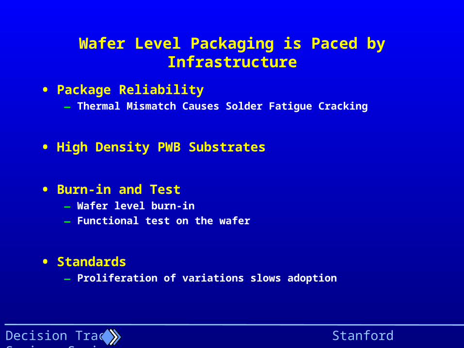
Wafer Level Packaging is Paced by Infrastructure
• Package Reliability– Thermal Mismatch Causes Solder Fatigue Cracking
• High Density PWB Substrates
• Burn-in and Test– Wafer level burn-in
– Functional test on the wafer
• Standards– Proliferation of variations slows adoption
Decision Track Stanford Seminar Series
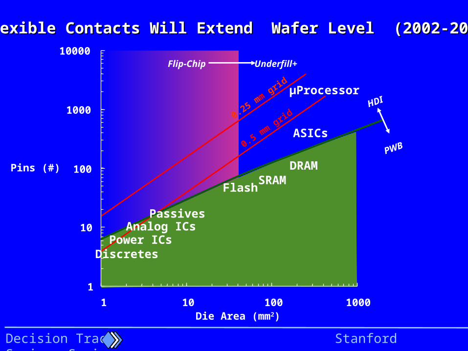
Die Area (mm2)
Pins (#)
1000
10000
10 100 1000
0.5 mm grid
0.25 mm grid µProcessor
10
100
1
1
ASICs
DRAM
FlashSRAM
Passives
Discretes
Flip-Chip Underfill+
HDI
PWB
Power ICsAnalog ICs

Decision Track Stanford Seminar Series
Flip-Chip Wafer Level Package
• Eutectic Solder Ball Flip-Chip– Small DNP allows adequate reliability
– Adapts existing infrastructure for rapid growth
. . . But --- limited to small die sizes
• Flexible Interconnect Extends to Larger Die Sizes– Metal columns
– Solder columns
– Stacked solder balls
– Flexible solder balls
. . . All with minimum changes to existing wafer processing infrastructure
• Wafer Level Package Provides:– Surface mountable package
– Testability
– Reliability
– Standards
Decision Track Stanford Seminar Series
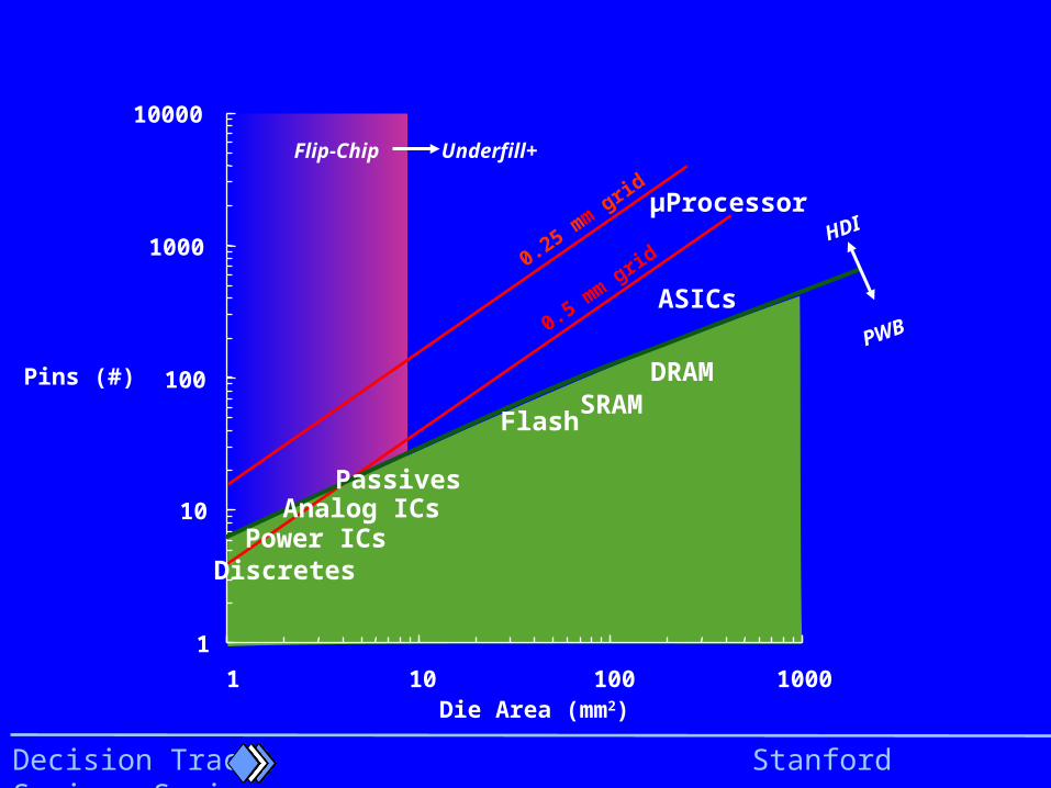
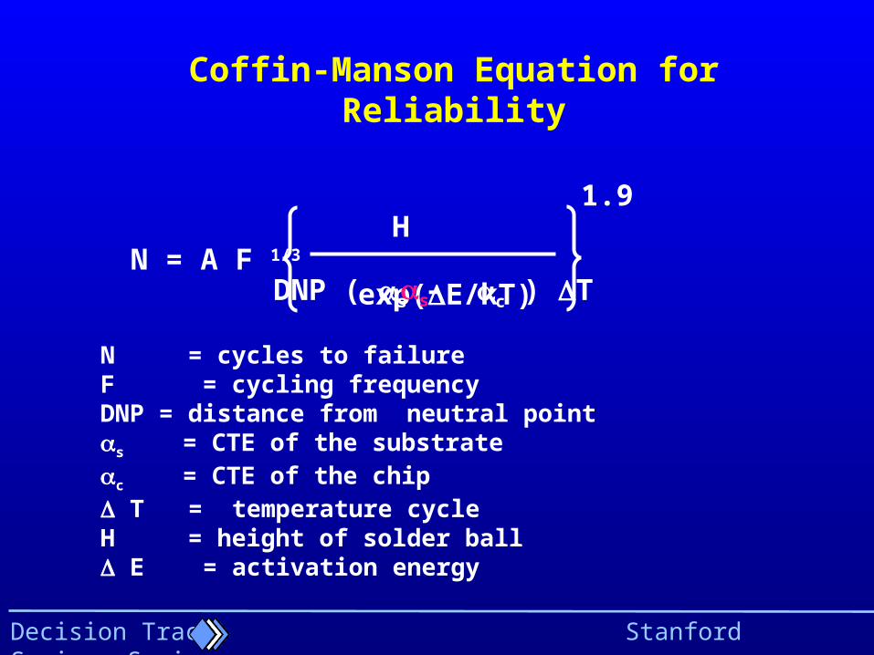
N = A F 1/3 exp(E/kT)DNP ( s - c ) T
H
N = cycles to failureF = cycling frequencyDNP = distance from neutral points = CTE of the substratec = CTE of the chip T = temperature cycleH = height of solder ball E = activation energy
1.9
Coffin-Manson Equation for Reliability
H

Decision Track Stanford Seminar Series
Fujitsu SuperCSPFujitsu SuperCSP
• Solder balls on copper posts
• Redistribution wiring to posts
• Encapsulant is molded onto wafer
• Inflexible posts limit reliability
Barrier Metal
Solder Ball Metal Post (Cu)
Encapsulant
Die
Polyimide Layer
Al Pad
RedistributionTrace (Cu) SiN

Decision Track Stanford Seminar Series
APACK Solder Column Package
Improves Strain Relief on Solder Ball
Decision Track Stanford Seminar Series
Die Area (mm2)
Pins (#)
1000
10000
10 100 1000
µProcessor
10
100
1
1
ASICs
DRAM
FlashSRAM
Passives
Discretes
Flip-Chip Underfill+
HDI
PWB
Power ICsAnalog ICs
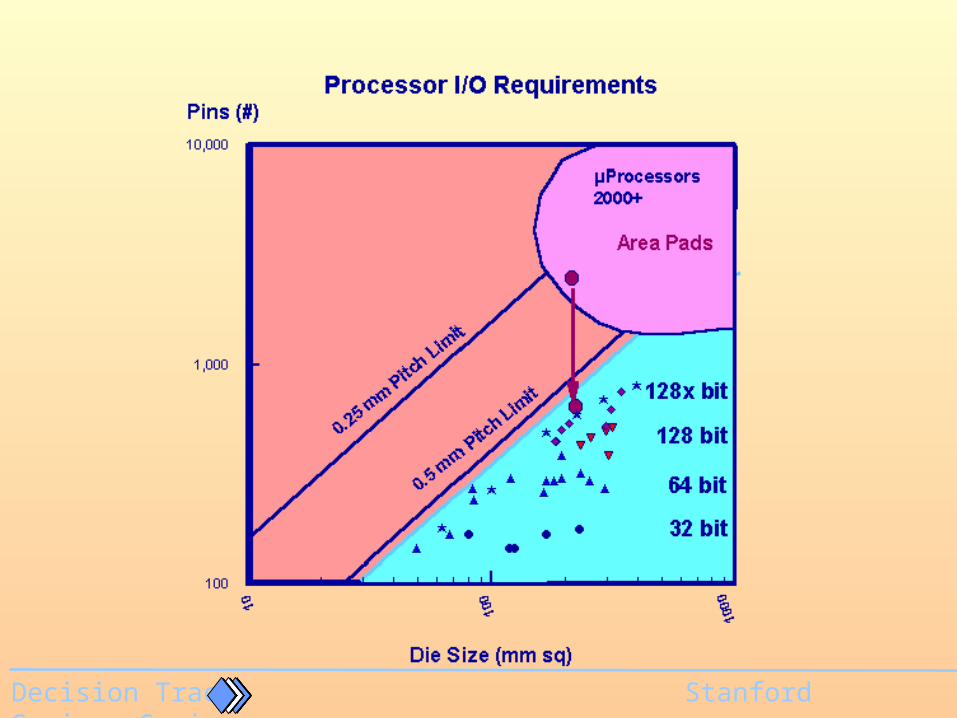
0.25 mm grid
0.5 mm grid
Flexible Contacts Will Extend Wafer Level (2002-2005)Flexible Contacts Will Extend Wafer Level (2002-2005)
Decision Track Stanford Seminar Series
DNP ( s - c ) TN = A F 1/3 exp(E/kT)
s
H
N = cycles to failureF = cycling frequencyDNP = distance from neutral points = CTE of the substratec = CTE of the chip T = temperature cycleH = height of solder ball E = activation energy
1.9
Coffin-Manson Equation for Reliability
Decision Track Stanford Seminar Series
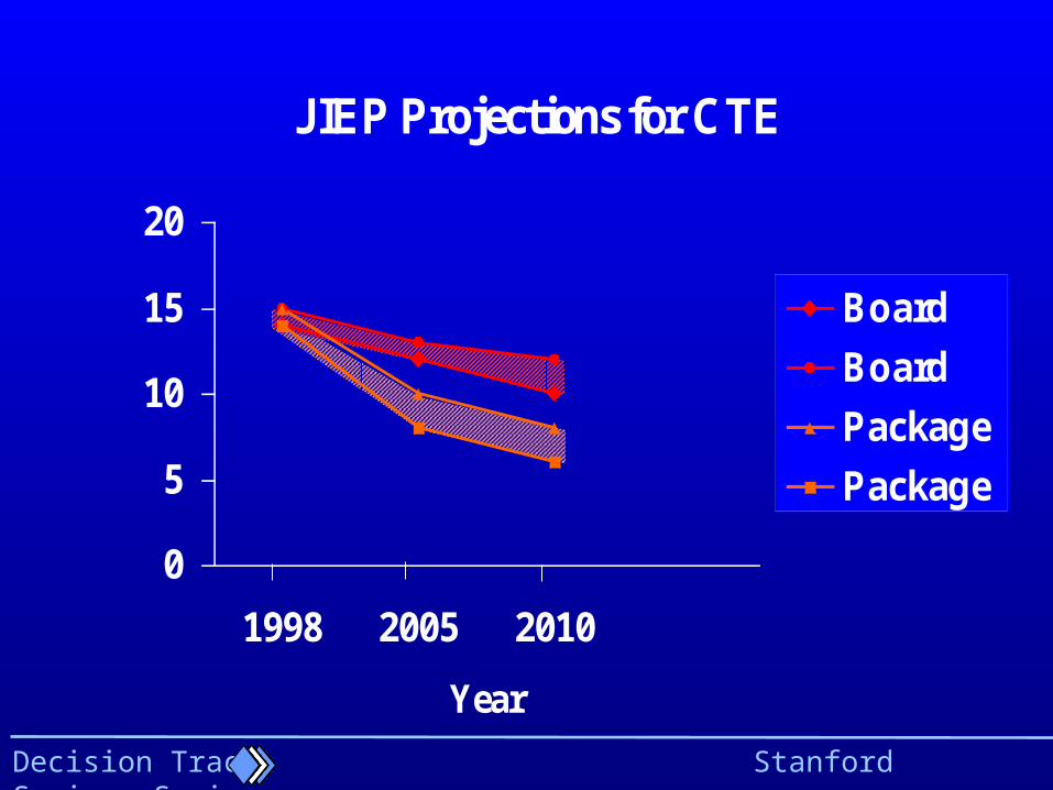
JIEP Projections for CTE
0
5
10
15
20
1998 2005 2010
Year
CTE (ppm/C)
Board
Board
Package
Package

Decision Track Stanford Seminar Series
IBM HPCC PackageIBM HPCC Package
D1D1D2D2D3D3
D4D4D5D5D6D6
Copper-Invar-Copper Core
Copper Circuit
Micro-vias
Eutectic Solder Ball
Direct Chip AttachPTFE Dielectric90Pb/10Sn Alloy
C-4 Solder Ball
Silicon Die
Solder Mask

Decision Track Stanford Seminar Series
Die Area (mm2)
Pins (#)
1000
10000
10 100 1000
10
100
1
1
ASICs
DRAM
FlashSRAM
Passives
Discretes
Flip-Chip
HDI
PWB
Power ICsAnalog ICs
0.25 mm grid
0.5 mm grid
Low CTE Substrates Further Extend Wafer Level (2005)Low CTE Substrates Further Extend Wafer Level (2005)
µProcessor

Decision Track Stanford Seminar Series
1995 2000 2005 2010
CSPWLP Paced by High Density Substrate
$ 5B
$10B
$15B
$20B
$25B
$30B
DRAMDSP
FLASH, SRAM
INFORMATONAPPLIANCES
µPROCESSOR
ASICsWLP
CSP
Requires HDI
WIRELESS
SiP
Stacked Die
Decision Track Stanford Seminar Series
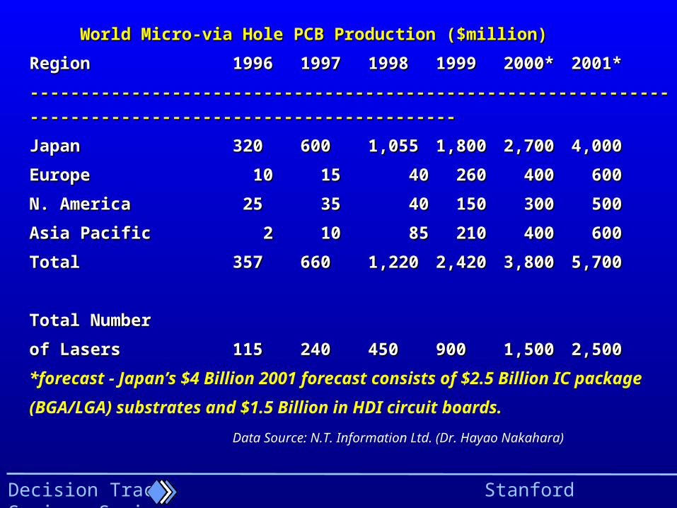
World Micro-via Hole PCB Production ($million)World Micro-via Hole PCB Production ($million)
RegionRegion 19961996 19971997 19981998 19991999 2000*2000* 2001*2001*
------------------------------------------------------------------------------------------------------------------------------------------------------------------------------------------------------------------
JapanJapan 320320 600600 1,0551,055 1,8001,800 2,7002,700 4,0004,000
EuropeEurope 10 10 15 15 40 40 260 260 400 400 600 600
N. AmericaN. America 25 25 35 35 40 40 150 150 300 300 500 500
Asia PacificAsia Pacific 2 2 10 10 85 85 210 210 400 400 600 600
TotalTotal 357357 660660 1,2201,220 2,4202,420 3,8003,800 5,7005,700
Total Number Total Number
of Lasersof Lasers 115115 240240 450450 900900 1,5001,500 2,5002,500
*forecast - Japan’s $4 Billion 2001 forecast consists of $2.5 Billion IC package
(BGA/LGA) substrates and $1.5 Billion in HDI circuit boards.
Data Source: N.T. Information Ltd. (Dr. Hayao Nakahara)

Decision Track Stanford Seminar Series
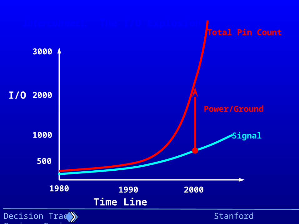
I/O Explosion: Power & Ground Distribution
• Distribute the Power and Ground on Chip
– Better electrical characteristics
– Shorter distance to the shielding planes
– Dramatically reduces I/O connections for power/ground
• 80+% of I/O on advanced processors is Power/Ground.
• Power and Ground Layers on the Wafer
– Efficiency of production
• Avoid paying for large number of power/ground pins.
– Makes the chip easier to test - fewer power/ground contacts
Decision Track Stanford Seminar Series
Decision Track Stanford Seminar Series
Interconnect: The I/O Explosion
I/O
Time Line
1980 1990 2000
500
2000
1000
3000
Signal
Total Pin Count
Power/Ground

Decision Track Stanford Seminar Series
Power & Ground: Redistribution on the Chip
Flip Chip• Pin count Explosion
• 70-80 % is Power & Ground
Power/Ground Distribution• Fabricated on separate layers
• Assembled to the wafer
Composite Chip• Power/ground distributed on the
chip to reduce I/O count
• High performance Power and ground distribution

Decision Track Stanford Seminar Series
Intra-Chip Communication: RC Delays
• RC Loading Limits Signal Propagation across Chip– R scales inversely with [lithographic dimension]2
– C remains ~ constant
– Problem gets worse with scaling to smaller dimension
• Reduce RC Delays– Lower Dielectric Constant of Insulator
– Copper Conductors to Reduce Resistance
– Wafer Level Packaging for High Performance Interconnect
• Impedance Controlled Nets
• Low RC
Decision Track Stanford Seminar Series
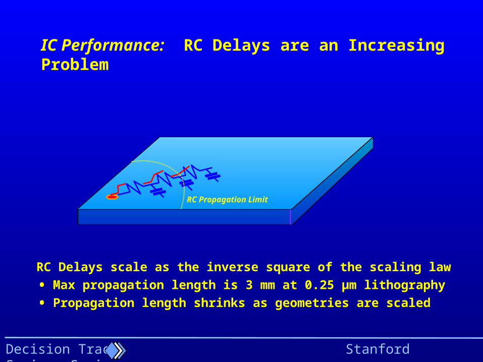
IC Performance: RC Delays are an Increasing Problem
RC Delays scale as the inverse square of the scaling law
• Max propagation length is 3 mm at 0.25 µm lithography
• Propagation length shrinks as geometries are scaled
RC Propagation Limit

Decision Track Stanford Seminar Series
IC Performance:IC Performance: Interconnect Dominates Delays* Interconnect Dominates Delays*
Performance 1.0 µm 0.1 µm
• Clock Speed 33 MHz 2-3.5 MHz• Wire Length 100 m 5000 m• Pin Count 150 to 3000
1.0 µm 0.1 µm
1 ps
10 ps
100 ps
MOSFET Delays
Package Delays
*SOURCE SEMI/SEMATECHInterconnect Focus Center
Decision Track Stanford Seminar Series
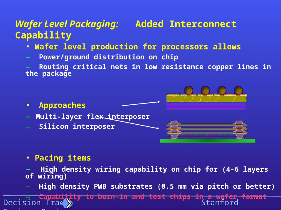
Wafer Level Packaging: Added Interconnect Capability
• Wafer level production for processors allows – Power/ground distribution on chip
– Routing critical nets in low resistance copper lines in the package
• Approaches
– Multi-layer flex interposer
– Silicon interposer
• Pacing items
– High density wiring capability on chip for (4-6 layers of wiring)
– High density PWB substrates (0.5 mm via pitch or better)
– Capability to burn-in and test chips in a wafer format
Decision Track Stanford Seminar Series
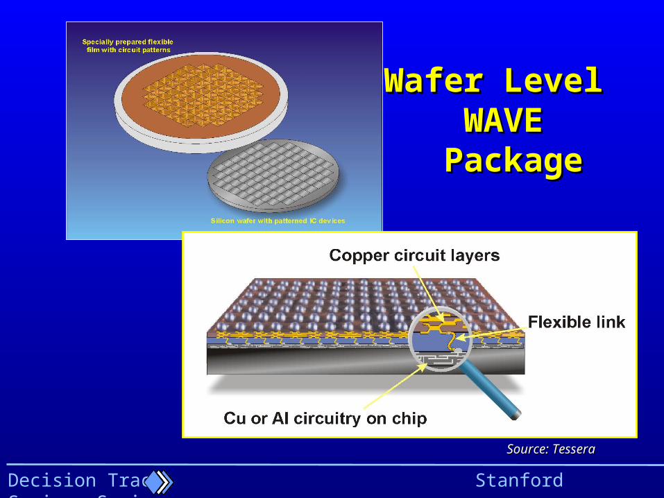
Wafer Level Wafer Level WAVE WAVE
PackagePackage
Source: TesseraSource: Tessera

Decision Track Stanford Seminar Series
X-ray imageX-ray imageof Flex-Linkof Flex-Link
Circuitized PolyimideCircuitized Polyimide
Copper Flex-Link Copper Flex-Link
Silicon WaferSilicon Wafer
Source: TesseraSource: Tessera

Decision Track Stanford Seminar Series
Multi-Chip Packages:Multi-Chip Packages: TruSi Stacked Wafers TruSi Stacked Wafers
Thru ViaThru Via
InsulationInsulation
PassivationPassivation
Decision Track Stanford Seminar Series
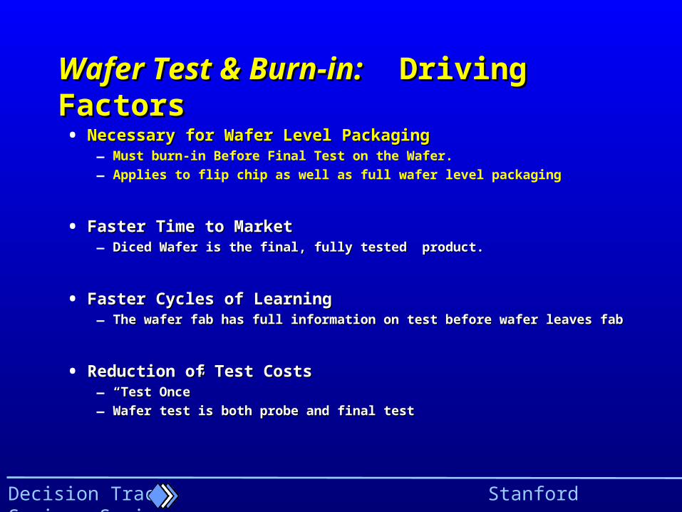
Wafer Test & Burn-in:Wafer Test & Burn-in: Driving Factors Driving Factors
• Necessary for Wafer Level PackagingNecessary for Wafer Level Packaging – Must burn-in Before Final Test on the Wafer.
– Applies to flip chip as well as full wafer level packaging
• Faster Time to MarketFaster Time to Market– Diced Wafer is the final, fully tested product.Diced Wafer is the final, fully tested product.
• Faster Cycles of LearningFaster Cycles of Learning– The wafer fab has full information on test before wafer leaves fabThe wafer fab has full information on test before wafer leaves fab
• Reduction of Test CostsReduction of Test Costs– ““Test Once”Test Once”
– Wafer test is both probe and final testWafer test is both probe and final test

Decision Track Stanford Seminar Series
WaferProbe
WaferDicing
Package
WaferBurn-in
WaferPackaging
FinalTest
WaferDicing
Package
Package
Test
Test
Test
Burn-in
Burn-in
Burn-in
Final Test
Final Test
Final Test
Conventional Packaging
Wafer Level Packaging•Product Cost Reduction•Cycle Time Reduction•Capital Cost Reduction
Wafer Run-inWafer Run-in

Decision Track Stanford Seminar Series
Process Flow:
Wafer Level Packaging vs.
Conventional Packaging
* From Motorola

Decision Track Stanford Seminar Series
Wafer Test:Wafer Test: Challenges Ahead Challenges Ahead
• Probe Density– 60 µm pad spacing
– Area array pads
• Functional Wafer Test– Test at Speed
• Parallel Testing– BIST ?
– Wafer run-in (test during burn-in)
• Hot chuck testing– Wafer test at temperatures to 150 oC

Decision Track Stanford Seminar Series
Wafer Burn-in:Wafer Burn-in: Technical Challenges Technical Challenges
• Contact Alignment
• Electrical Interconnect– Wire 10,000 - 20,000 contacts to device drivers
• Large Number of Electrical Contacts– Force of 250 lb for 20,000 contacts
– 500,000 contacts for a flip chip micro-Processor
• Extreme Environment

Decision Track Stanford Seminar Series
Wafer Burn-in:Wafer Burn-in: Technical Challenges Technical Challenges
From 25C to 150C
Cu 450 µm (18 mils)
Si 75 µm (3 mils)
10,000 - 500,000 contacts

Decision Track Stanford Seminar Series
The Drive Toward Wafer Level Packaging The Drive Toward Wafer Level Packaging
• Chip Scale Packages are Replacing Conventional PackagesInitial applications are rapidly growing personal electronics CSPs move toward Wafer Level Production
• Growth of Chip Scale Electronics will be RapidCSP/WLP will grow to a $40B market in 10 years timeRapidly growing approaches use existing infrastructure
• Wafer Level Packaging will Extend CSP for Decades into the FuturePackaging and wafer fabrication will mergeAdditional function is integrated into the package
• Wafer Level Technologies will Provide Added Functionality
Intra-Chip InterconnectPower/Ground DistributionStacked Wafers