DDR4 Compliance Test Bench - Keysightedadownload.software.keysight.com/eedl/ads/2016_01/... · the...
57
Transcript of DDR4 Compliance Test Bench - Keysightedadownload.software.keysight.com/eedl/ads/2016_01/... · the...

DDR4 Compliance Test Bench
ADS 2016.01
Notice© Keysight Technologies, Inc. 1983-2016
1400 Fountaingrove Pkwy., Santa Rosa, CA 95403-1738, United States
All rights reserved.
No part of this documentation may be reproduced in any form or by any means (including electronic storage
and retrieval or translation into a foreign language) without prior agreement and written consent from
Keysight Technologies, Inc. as governed by United States and international copyright laws.
Restricted Rights Legend
If software is for use in the performance of a U.S. Government prime contract or subcontract, Software is
delivered and licensed as "Commercial computer software" as defined in DFAR 252.227-7014 (June 1995),
or as a "commercial item" as defined in FAR 2.101(a) or as "Restricted computer software" as defined in FAR
52.227-19 (June 1987) or any equivalent agency regulation or contract clause.
Use, duplication or disclosure of Software is subject to Keysight Technologies' standard commercial license
terms, and non-DOD Departments and Agencies of the U.S. Government will receive no greater than
Restricted Rights as defined in FAR 52.227-19(c)(1-2) (June 1987). U.S. Government users will receive no
greater than Limited Rights as defined in FAR 52.227-14 (June 1987) or DFAR 252.227-7015 (b)(2)
(November 1995), as applicable in any technical data.
Acknowledgments
Layout Boolean Engine by Klaas Holwerda, v1.7 http://boolean.klaasholwerda.nl/bool.html
FreeType Project, Copyright (c) 1996-1999 by David Turner, Robert Wilhelm, and Werner Lemberg.
QuestAgent search engine (c) 2000-2002, JObjects.
Portions of the code Copyright (c) 1990-1996
The Regents of the University of California. All rights reserved. Permission is hereby granted, without written
agreement and without license or royalty fees, to use, modify and distribute the Ptolemy software and its
documentation for any purpose, provided that the above copyright notice and the following two paragraphs
appear in all copies of the software and documentation.
In no event shall the University of California be liable to any party for direct, indirect, special, incidental, or
consequential damages arising out of the use of this software and its documentation, even if the University
of California has been advised of the possibility of such damage.
The University of California specifically disclaims any warranties, including, but not limited to, the implied
warranties of merchantability and fitness for a particular purpose. The software provided hereunder is on an
"as is" basis and the University of California has no obligation to provide maintenance, support, updates,
enhancements, or modifications.
Portions of this product include the SystemC software licensed under Open Source terms, which are
available for download at . This software is redistributed by Keysight. The Contributors of http://systemc.org/
the SystemC software provide this software "as is" and offer no warranty of any kind, express or implied,
including without limitation warranties or conditions or title and non-infringement, and implied warranties or
conditions merchantability and fitness for a particular purpose. Contributors shall not be liable for any
damages of any kind including without limitation direct, indirect, special, incidental and consequential
damages, such as lost profits. Any provisions that differ from this disclaimer are offered by Keysight only.
Motif is a trademark of the Open Software Foundation.
Netscape is a trademark of Netscape Communications Corporation.
UNIX is a registered trademark of the Open Group.
Microsoft, Windows, Windows NT, Windows 2000, and Windows Internet Explorer are registered trademarks
of Microsoft Corporation in the United States and other countries.
Pentium is a registered trademark of Intel Corporation.
Acrobat, PDF, and PostScript are registered trademarks of Adobe Systems Incorporated.
FLEXlm and FLEXnet are registered trademarks of Flexera Software LLC Terms of Use for Flexera Software
information can be found at http://www.flexerasoftware.com/company/about/terms.htm
Netscape Portable Runtime (NSPR), Copyright (c) 1998-2003 The Mozilla Organization. A copy of the Mozilla
Public License is at http://www.mozilla.org/MPL/
FFTW, The Fastest Fourier Transform in the West, Copyright (c) 1997-1999 Massachusetts Institute of
Technology. All rights reserved.
Oracle and Java are registered trademarks of Oracle and/or its affiliates. Other names may be trademarks of
their respective owners.
Cadence, Allegro, Assura, Dracula, SKILL, Spectre, and Virtuoso are registered trademarks of Cadence
Design Systems, Inc. in the United States and/or other jurisdictions.
Mentor, Mentor Graphics, Board Station, Calibre, and Expedition are registered trademarks of Mentor
Graphics Corporation in the United States and other countries.
SystemC is a registered trademark of Open SystemC Initiative, Inc. in the United States and other countries
and is used with permission.
Gradient, HeatWave and FireBolt are trademarks of Gradient Design Automation Inc.
The following third-party libraries are used by the NlogN Momentum solver:
Metis 4.0, Copyright © 1998, Regents of the University of Minnesota", , http://www.cs.umn.edu/~metis
METIS was written by George Karypis ([email protected]).
Intel@ Math Kernel Library, http://www.intel.com/software/products/mkl
HSPICE is a registered trademark of Synopsys, Inc. in the United States and/or other countries.
DWG and DXF are registered trademarks of Autodesk, Inc. in the United States and/or other countries.
1.
2.
MATLAB is a registered trademark of The MathWorks, Inc. in the United States and/or other countries.
SuperLU_MT version 2.0
SuperLU Copyright: Copyright © 2003, The Regents of the University of California, through Lawrence
Berkeley National Laboratory (subject to receipt of any required approvals from U.S. Dept. of Energy). All
rights reserved.
SuperLU Disclaimer: THIS SOFTWARE IS PROVIDED BY THE COPYRIGHT HOLDERS AND CONTRIBUTORS
"AS IS" AND ANY EXPRESS OR IMPLIED WARRANTIES, INCLUDING, BUT NOT LIMITED TO, THE IMPLIED
WARRANTIES OF MERCHANTABILITY AND FITNESS FOR A PARTICULAR PURPOSE ARE DISCLAIMED. IN NO
EVENT SHALL THE COPYRIGHT OWNER OR CONTRIBUTORS BE LIABLE FOR ANY DIRECT, INDIRECT,
INCIDENTAL, SPECIAL, EXEMPLARY, OR CONSEQUENTIAL DAMAGES (INCLUDING, BUT NOT LIMITED TO,
PROCUREMENT OF SUBSTITUTE GOODS OR SERVICES; LOSS OF USE, DATA, OR PROFITS; OR BUSINESS
INTERRUPTION) HOWEVER CAUSED AND ON ANY THEORY OF LIABILITY, WHETHER IN CONTRACT, STRICT
LIABILITY, OR TORT (INCLUDING NEGLIGENCE OR OTHERWISE) ARISING IN ANY WAY OUT OF THE USE OF
THIS SOFTWARE, EVEN IF ADVISED OF THE POSSIBILITY OF SUCH DAMAGE.
7-zip
7-Zip Copyright: Copyright (C) 1999-2009 Igor Pavlov.
Licenses for files are:
7z.dll: GNU LGPL + unRAR restriction.
All other files: GNU LGPL.
7-zip License: This library is free software; you can redistribute it and/or modify it under the terms of the
GNU Lesser General Public License as published by the Free Software Foundation; either version 2.1 of the
License, or (at your option) any later version. This library is distributed in the hope that it will be useful,but
WITHOUT ANY WARRANTY; without even the implied warranty of MERCHANTABILITY or FITNESS FOR A
PARTICULAR PURPOSE. See the GNU Lesser General Public License for more details. You should have
received a copy of the GNU Lesser General Public License along with this library; if not, write to the Free
Software Foundation, Inc., 59 Temple Place, Suite 330, Boston, MA 02111-1307 USA.
unRAR copyright: The decompression engine for RAR archives was developed using source code of unRAR
program.All copyrights to original unRAR code are owned by Alexander Roshal.
unRAR License: The unRAR sources cannot be used to re-create the RAR compression algorithm, which is
proprietary. Distribution of modified unRAR sources in separate form or as a part of other software is
permitted, provided that it is clearly stated in the documentation and source comments that the code may
not be used to develop a RAR (WinRAR) compatible archiver.
7-zip Availability: http://www.7-zip.org/
AMD Version 2.2
AMD Notice: The AMD code was modified. Used by permission.
AMD copyright: AMD Version 2.2, Copyright © 2007 by Timothy A. Davis, Patrick R. Amestoy, and Iain S.
Duff. All Rights Reserved.
AMD License: Your use or distribution of AMD or any modified version of AMD implies that you agree to this
License. This library is free software; you can redistribute it and/or modify it under the terms of the GNU
Lesser General Public License as published by the Free Software Foundation; either version 2.1 of the
License, or (at your option) any later version. This library is distributed in the hope that it will be useful, but
WITHOUT ANY WARRANTY; without even the implied warranty of MERCHANTABILITY or FITNESS FOR A
PARTICULAR PURPOSE. See the GNU Lesser General Public License for more details. You should have
received a copy of the GNU Lesser General Public License along with this library; if not, write to the Free
Software Foundation, Inc., 51 Franklin St, Fifth Floor, Boston, MA 02110-1301 USA Permission is hereby
granted to use or copy this program under the terms of the GNU LGPL, provided that the Copyright, this
License, and the Availability of the original version is retained on all copies.User documentation of any code
that uses this code or any modified version of this code must cite the Copyright, this License, the Availability
note, and "Used by permission." Permission to modify the code and to distribute modified code is granted,
provided the Copyright, this License, and the Availability note are retained, and a notice that the code was
modified is included.
AMD Availability: http://www.cise.ufl.edu/research/sparse/amd
UMFPACK 5.0.2
UMFPACK Notice: The UMFPACK code was modified. Used by permission.
UMFPACK Copyright: UMFPACK Copyright © 1995-2006 by Timothy A. Davis. All Rights Reserved.
UMFPACK License: Your use or distribution of UMFPACK or any modified version of UMFPACK implies that
you agree to this License. This library is free software; you can redistribute it and/or modify it under the
terms of the GNU Lesser General Public License as published by the Free Software Foundation; either version
2.1 of the License, or (at your option) any later version. This library is distributed in the hope that it will be
useful, but WITHOUT ANY WARRANTY; without even the implied warranty of MERCHANTABILITY or FITNESS
FOR A PARTICULAR PURPOSE. See the GNU Lesser General Public License for more details. You should have
received a copy of the GNU Lesser General Public License along with this library; if not, write to the Free
Software Foundation, Inc., 51 Franklin St, Fifth Floor, Boston, MA 02110-1301 USA Permission is hereby
granted to use or copy this program under the terms of the GNU LGPL, provided that the Copyright, this
License, and the Availability of the original version is retained on all copies. User documentation of any code
that uses this code or any modified version of this code must cite the Copyright, this License, the Availability
note, and "Used by permission." Permission to modify the code and to distribute modified code is granted,
provided the Copyright, this License, and the Availability note are retained, and a notice that the code was
modified is included.
UMFPACK Availability: UMFPACK (including versions http://www.cise.ufl.edu/research/sparse/umfpack
2.2.1 and earlier, in FORTRAN) is available at . MA38 is available in http://www.cise.ufl.edu/research/sparse
the Harwell Subroutine Library. This version of UMFPACK includes a modified form of COLAMD Version 2.0,
originally released on Jan. 31, 2000, also available at . COLAMD V2.http://www.cise.ufl.edu/research/sparse
0 is also incorporated as a built-in function in MATLAB version 6.1, by The MathWorks, Inc. http://www.
. COLAMD V1.0 appears as a column-preordering in SuperLU (SuperLU is available at mathworks.com
). UMFPACK v4.0 is a built-in routine in MATLAB 6.5. UMFPACK v4.3 is a built-in http://www.netlib.org
routine in MATLAB 7.1.
Errata
The ADS product may contain references to "HP" or "HPEESOF" such as in file names and directory names.
The business entity formerly known as "HP EEsof" is now part of Keysight Technologies and is known as
"Keysight EEsof". To avoid broken functionality and to maintain backward compatibility for our customers,
we did not change all the names and labels that contain "HP" or "HPEESOF" references.
Qt Version 4.8.4
Qt Notice: The Qt code was modified. Used by permission.
Qt Version 4.8.4, Copyright (C) 2014 Digia Plc and/or its subsidiary(-ies). All Rights Reserved. Contact:
http://www.qt-project.org/legal
Qt License: . Your use or distribution of Qt or any modified version http://qt-project.org/doc/qt-4.8/lgpl.html
of Qt implies that you agree to this License. This library is free software; you can redistribute it and/or modify
it under the terms of the GNU Lesser General Public License as published by the Free Software Foundation;
either version 2.1 of the License, or (at your option) any later version. This library is distributed in the hope
that it will be useful, but WITHOUT ANY WARRANTY; without even the implied warranty of
MERCHANTABILITY or FITNESS FOR A PARTICULAR PURPOSE. See the GNU Lesser General Public License
for more details. You should have received a copy of the GNU Lesser General Public License along with this
library; if not, write to the Free Software Foundation, Inc., 51 Franklin St, Fifth Floor, Boston, MA 02110-
1301 USA Permission is hereby granted to use or copy this program under the terms of the GNU LGPL,
provided that the Copyright, this License, and the Availability of the original version is retained on all copies.
User documentation of any code that uses this code or any modified version of this code must cite the
Copyright, this License, the Availability note, and "Used by permission." Permission to modify the code and to
distribute modified code is granted, provided the Copyright, this License, and the Availability note are
retained, and a notice that the code was modified is included.
Qt Availability: http://www.qtsoftware.com/downloads
Patches Applied to Qt can be found in the installation at: $HPEESOF_DIR/prod/licenses/thirdparty/qt
/patches.
You may also contact Brian Buchanan at Keysight Inc. at [email protected] for more
information.
The HiSIM_HV source code, and all copyrights, trade secrets or other intellectual property rights in and to
the source code, is owned by Hiroshima University and/or STARC.
HDF5
HDF5 Notice: The HDF5 code was modified. Used by permission.
HDF5 Copyright: Copyright 2006-2013 by The HDF Group.
HDF5 License:
Copyright Notice and License Terms for HDF5 (Hierarchical Data Format 5) Software Library and Utilities
------------------------------------------------------------------------------------------------------------------------------------------------------
HDF5 (Hierarchical Data Format 5) Software Library and Utilities
Copyright 2006-2013 by The HDF Group.
1.
2.
3.
4.
5.
NCSA HDF5 (Hierarchical Data Format 5) Software Library and Utilities
Copyright 1998-2006 by the Board of Trustees of the University of Illinois.
All rights reserved.
Redistribution and use in source and binary forms, with or without modification, are permitted for any
purpose (including commercial purposes) provided that the following conditions are met:
Redistributions of source code must retain the above copyright notice, this list of conditions, and the
following disclaimer.
Redistributions in binary form must reproduce the above copyright notice, this list of conditions, and
the following disclaimer in the documentation and/or materials provided with the distribution.
In addition, redistributions of modified forms of the source or binary code must carry prominent
notices stating that the original code was changed and the date of the change.
All publications or advertising materials mentioning features or use of this software are asked, but not
required, to acknowledge that it was developed by The HDF Group and by the National Center for
Supercomputing Applications at the University of Illinois at Urbana-Champaign and credit the
contributors.
Neither the name of The HDF Group, the name of the University, nor the name of any Contributor may
be used to endorse or promote products derived from this software without specific prior written
permission from The HDF Group, the University, or the Contributor, respectively.
libpng
libpng Copyright: libpng versions 1.2.6, August 15, 2004, through 1.6.3, July 18, 2013, are Copyright (c)
2004, 2006-2013.
libpng License: This copy of the libpng notices is provided for your convenience. In case of any discrepancy
between this copy and the notices in the file png.h that is included in the libpng distribution, the latter shall
prevail.
COPYRIGHT NOTICE, DISCLAIMER, and LICENSE:
If you modify libpng you may insert additional notices immediately following this sentence.
This code is released under the libpng license.
libpng versions 1.2.6, August 15, 2004, through 1.6.3, July 18, 2013, are Copyright (c) 2004, 2006-2013
Glenn Randers-Pehrson, and are distributed according to the same disclaimer and license as libpng-1.2.5
with the following individual added to the list of Contributing Authors, Cosmin Truta
libpng versions 1.0.7, July 1, 2000, through 1.2.5 - October 3, 2002, are Copyright (c) 2000-2002 Glenn
Randers-Pehrson, and are distributed according to the same disclaimer and license as libpng-1.0.6 with the
following individuals added to the list of Contributing Authors
Simon-Pierre Cadieux, Eric S. Raymond, Gilles Vollant and with the following additions to the disclaimer:
There is no warranty against interference with your enjoyment of the library or against infringement. There is
no warranty that our efforts or the library will fulfill any of your particular purposes or needs. This library is
provided with all faults, and the entire risk of satisfactory quality, performance, accuracy, and effort is with
the user.
1.
2.
3.
1.
2.
libpng versions 0.97, January 1998, through 1.0.6, March 20, 2000, are Copyright (c) 1998, 1999 Glenn
Randers-Pehrson, and are distributed according to the same disclaimer and license as libpng-0.96, with the
following individuals added to the list of Contributing Authors: Tom Lane, Glenn Randers-Pehrson, Willem
van Schaik
libpng versions 0.89, June 1996, through 0.96, May 1997, are Copyright (c) 1996, 1997 Andreas Dilger
Distributed according to the same disclaimer and license as libpng-0.88, with the following individuals added
to the list of Contributing Authors: John Bowler, Kevin Bracey, Sam Bushell, Magnus Holmgren, Greg
Roelofs, Tom Tanner
libpng versions 0.5, May 1995, through 0.88, January 1996, are Copyright (c) 1995, 1996 Guy Eric Schalnat,
Group 42, Inc.
For the purposes of this copyright and license, "Contributing Authors" is defined as the following set of
individuals: Andreas Dilger, Dave Martindale, Guy Eric Schalnat, Paul Schmidt, Tim Wegner
The PNG Reference Library is supplied "AS IS". The Contributing Authors and Group 42, Inc. disclaim all
warranties, expressed or implied, including, without limitation, the warranties of merchantability and of
fitness for any purpose. The Contributing Authors and Group 42, Inc. assume no liability for direct, indirect,
incidental, special, exemplary, or consequential damages, which may result from the use of the PNG
Reference Library, even if advised of the possibility of such damage.
Permission is hereby granted to use, copy, modify, and distribute this source code, or portions hereof, for any
purpose, without fee, subject to the following restrictions:
The origin of this source code must not be misrepresented.
Altered versions must be plainly marked as such and must not be misrepresented as being the original
source.
This Copyright notice may not be removed or altered from any source or altered source distribution.
The Contributing Authors and Group 42, Inc. specifically permit, without fee, and encourage the use of this
source code as a component to supporting the PNG file format in commercial products. If you use this
source code in a product, acknowledgment is not required but would be appreciated.
OpenSSL
The OpenSSL toolkit stays under a dual license, i.e. both the conditions of the OpenSSL License and the
original SSLeay license apply to the toolkit. See below for the actual license texts. Actually both licenses are
BSD-style Open Source licenses. In case of any license issues related to OpenSSL please contact openssl-
OpenSSL License
---------------
====================================================================
Copyright (c) 1998-2011 The OpenSSL Project. All rights reserved.
Redistribution and use in source and binary forms, with or without modification, are permitted provided that
the following conditions are met:
Redistributions of source code must retain the above copyright notice, this list of conditions and the
following disclaimer.
Redistributions in binary form must reproduce the above copyright notice, this list of conditions and
the following disclaimer in the documentation and/or other materials provided with the distribution.
3.
4.
5.
6.
1.
2.
All advertising materials mentioning features or use of this software must display the following
acknowledgment: "This product includes software developed by the OpenSSL Project for use in the
OpenSSL Toolkit. ( )"http://www.openssl.org/
The names "OpenSSL Toolkit" and "OpenSSL Project" must not be used to endorse or promote
products derived from this software without prior written permission. For written permission, please
contact [email protected]
Products derived from this software may not be called "OpenSSL" nor may "OpenSSL" appear in their
names without prior written permission of the OpenSSL Project.
Redistributions of any form whatsoever must retain the following acknowledgment: "This product
includes software developed by the OpenSSL Project for use in the OpenSSL Toolkit (http://www.
)"openssl.org/
THIS SOFTWARE IS PROVIDED BY THE OpenSSL PROJECT "AS IS" AND ANY EXPRESSED OR IMPLIED
WARRANTIES, INCLUDING, BUT NOT LIMITED TO, THE IMPLIED WARRANTIES OF MERCHANTABILITY AND
FITNESS FOR A PARTICULAR PURPOSE ARE DISCLAIMED. IN NO EVENT SHALL THE OpenSSL PROJECT OR
ITS CONTRIBUTORS BE LIABLE FOR ANY DIRECT, INDIRECT, INCIDENTAL, SPECIAL, EXEMPLARY, OR
CONSEQUENTIAL DAMAGES (INCLUDING, BUT NOT LIMITED TO, PROCUREMENT OF SUBSTITUTE GOODS
OR SERVICES; LOSS OF USE, DATA, OR PROFITS; OR BUSINESS INTERRUPTION) HOWEVER CAUSED AND
ON ANY THEORY OF LIABILITY, WHETHER IN CONTRACT, STRICT LIABILITY, OR TORT (INCLUDING
NEGLIGENCE OR OTHERWISE) ARISING IN ANY WAY OUT OF THE USE OF THIS SOFTWARE, EVEN IF
ADVISED OF THE POSSIBILITY OF SUCH DAMAGE.
====================================================================
This product includes cryptographic software written by Eric Young ( ). This product [email protected]
includes software written by Tim Hudson ( )[email protected]
Original SSLeay License
-----------------------
Copyright (C) 1995-1998 Eric Young ( )[email protected]
All rights reserved.
This package is an SSL implementation written by Eric Young ( )[email protected]
The implementation was written so as to conform with Netscapes SSL. This library is free for commercial and
non-commercial use as long as the following conditions are aheared to. The following conditions apply to all
code found in this distribution, be it the RC4, RSA, lhash, DES, etc., code; not just the SSL code. The SSL
documentation included with this distribution is covered by the same copyright terms except that the holder
is Tim Hudson ( )[email protected]
Copyright remains Eric Young's, and as such any Copyright notices in the code are not to be removed. If this
package is used in a product, Eric Young should be given attribution as the author of the parts of the library
used. This can be in the form of a textual message at program startup or in documentation (online or textual)
provided with the package.
Redistribution and use in source and binary forms, with or without modification, are permitted provided that
the following conditions are met:
Redistributions of source code must retain the copyright notice, this list of conditions and the
following disclaimer.
Redistributions in binary form must reproduce the above copyright notice, this list of conditions and
the following disclaimer in the documentation and/or other materials provided with the distribution.
3.
4.
1.
2.
3.
All advertising materials mentioning features or use of this software must display the following
acknowledgement: "This product includes cryptographic software written by Eric Young (
)" The word 'cryptographic' can be left out if the rouines from the library being [email protected]
used are not cryptographic related.
If you include any Windows specific code (or a derivative thereof) from the apps directory (application
code) you must include an acknowledgement: "This product includes software written by Tim Hudson (
THIS SOFTWARE IS PROVIDED BY ERIC YOUNG ``AS IS'' AND ANY EXPRESS OR IMPLIED WARRANTIES,
INCLUDING, BUT NOT LIMITED TO, THE IMPLIED WARRANTIES OF MERCHANTABILITY AND FITNESS FOR A
PARTICULAR PURPOSE ARE DISCLAIMED. IN NO EVENT SHALL THE AUTHOR OR CONTRIBUTORS BE LIABLE
FOR ANY DIRECT, INDIRECT, INCIDENTAL, SPECIAL, EXEMPLARY, OR CONSEQUENTIAL DAMAGES
(INCLUDING, BUT NOT LIMITED TO, PROCUREMENT OF SUBSTITUTE GOODS OR SERVICES; LOSS OF USE,
DATA, OR PROFITS; OR BUSINESS INTERRUPTION) HOWEVER CAUSED AND ON ANY THEORY OF LIABILITY,
WHETHER IN CONTRACT, STRICT LIABILITY, OR TORT (INCLUDING NEGLIGENCE OR OTHERWISE) ARISING
IN ANY WAY OUT OF THE USE OF THIS SOFTWARE, EVEN IF ADVISED OF THE POSSIBILITY OF SUCH
DAMAGE.
The licence and distribution terms for any publically available version or derivative of this code cannot be
changed. i.e. this code cannot simply be copied and put under another distribution license \[including the
GNU Public Licence.]
Growl GNTP support:
[The "BSD licence"] Copyright (c) 2009-2010 Yasuhiro Matsumoto
All rights reserved.
Redistribution and use in source and binary forms, with or without modification, are permitted provided that
the following conditions are met:
Redistributions of source code must retain the above copyright notice, this list of conditions and the
following disclaimer.
Redistributions in binary form must reproduce the above copyright notice, this list of conditions and
the following disclaimer in the documentation and/or other materials provided with the distribution.
The name of the author may not be used to endorse or promote products derived from this software
without specific prior written permission.
THIS SOFTWARE IS PROVIDED BY THE AUTHOR "AS IS'' AND ANY EXPRESS OR IMPLIED WARRANTIES,
INCLUDING, BUT NOT LIMITED TO, THE IMPLIED WARRANTIES OF MERCHANTABILITY AND FITNESS FOR A
PARTICULAR PURPOSE ARE DISCLAIMED. IN NO EVENT SHALL THE AUTHOR BE LIABLE FOR ANY DIRECT,
INDIRECT, INCIDENTAL, SPECIAL, EXEMPLARY, OR CONSEQUENTIAL DAMAGES (INCLUDING, BUT NOT
LIMITED TO, PROCUREMENT OF SUBSTITUTE GOODS OR SERVICES; LOSS OF USE, DATA, OR PROFITS; OR
BUSINESS INTERRUPTION) HOWEVER CAUSED AND ON ANY THEORY OF LIABILITY, WHETHER IN
CONTRACT, STRICT LIABILITY, OR TORT (INCLUDING NEGLIGENCE OR OTHERWISE) ARISING IN ANY WAY
OUT OF THE USE OF THIS SOFTWARE, EVEN IF ADVISED OF THE POSSIBILITY OF SUCH DAMAGE.
Cuda
Cuda Redistributable Software - 1.8. Attachment A
---------------------------------
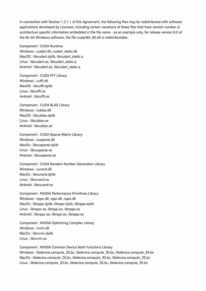
In connection with Section 1.2.1.1 of this Agreement, the following files may be redistributed with software
applications developed by Licensee, including certain variations of these files that have version number or
architecture specific information embedded in the file name - as an example only, for release version 6.0 of
the 64-bit Windows software, the file cudart64_60.dll is redistributable.
Component : CUDA Runtime
Windows : cudart.dll, cudart_static.lib
MacOS : libcudart.dylib, libcudart_static.a
Linux : libcudart.so, libcudart_static.a
Android : libcudart.so, libcudart_static.a
Component : CUDA FFT Library
Windows : cufft.dll
MacOS : libcufft.dylib
Linux : libcufft.so
Android : libcufft.so
Component : CUDA BLAS Library
Windows : cublas.dll
MacOS : libcublas.dylib
Linux : libcublas.so
Android : libcublas.so
Component : CUDA Sparse Matrix Library
Windows : cusparse.dll
MacOs : libcusparse.dylib
Linux : libcusparse.so
Android : libcusparse.so
Component : CUDA Random Number Generation Library
Windows : curand.dll
MacOs : libcurand.dylib
Linux : libcurand.so
Android : libcurand.so
Component : NVIDIA Performance Primitives Library
Windows : nppc.dll, nppi.dll, npps.dll
MacOs : libnppc.dylib, libnppi.dylib, libnpps.dylib
Linux : libnppc.so, libnppi.so, libnpps.so
Android : libnppc.so, libnppi.so, libnpps.so
Component : NVIDIA Optimizing Compiler Library
Windows : nvvm.dll
MacOs : libnvvm.dylib
Linux : libnvvm.so
Component : NVIDIA Common Device Math Functions Library
Windows : libdevice.compute_20.bc, libdevice.compute_30.bc, libdevice.compute_35.bc
MacOs : libdevice.compute_20.bc, libdevice.compute_30.bc, libdevice.compute_35.bc
Linux : libdevice.compute_20.bc, libdevice.compute_30.bc, libdevice.compute_35.bc
Component : CUDA Occupancy Calculation Header Library
All : cuda_occupancy.h
Read more at: http://docs.nvidia.com/cuda/eula/index.html#ixzz30CrknWfU
Warranty The material contained in this document is provided "as is", and is subject to being changed,
without notice, in future editions. Further, to the maximum extent permitted by applicable law, Keysight
disclaims all warranties, either express or implied, with regard to this documentation and any information
contained herein, including but not limited to the implied warranties of merchantability and fitness for a
particular purpose. Keysight shall not be liable for errors or for incidental or consequential damages in
connection with the furnishing, use, or performance of this document or of any information contained herein.
Should Keysight and the user have a separate written agreement with warranty terms covering the material
in this document that conflict with these terms, the warranty terms in the separate agreement shall control.
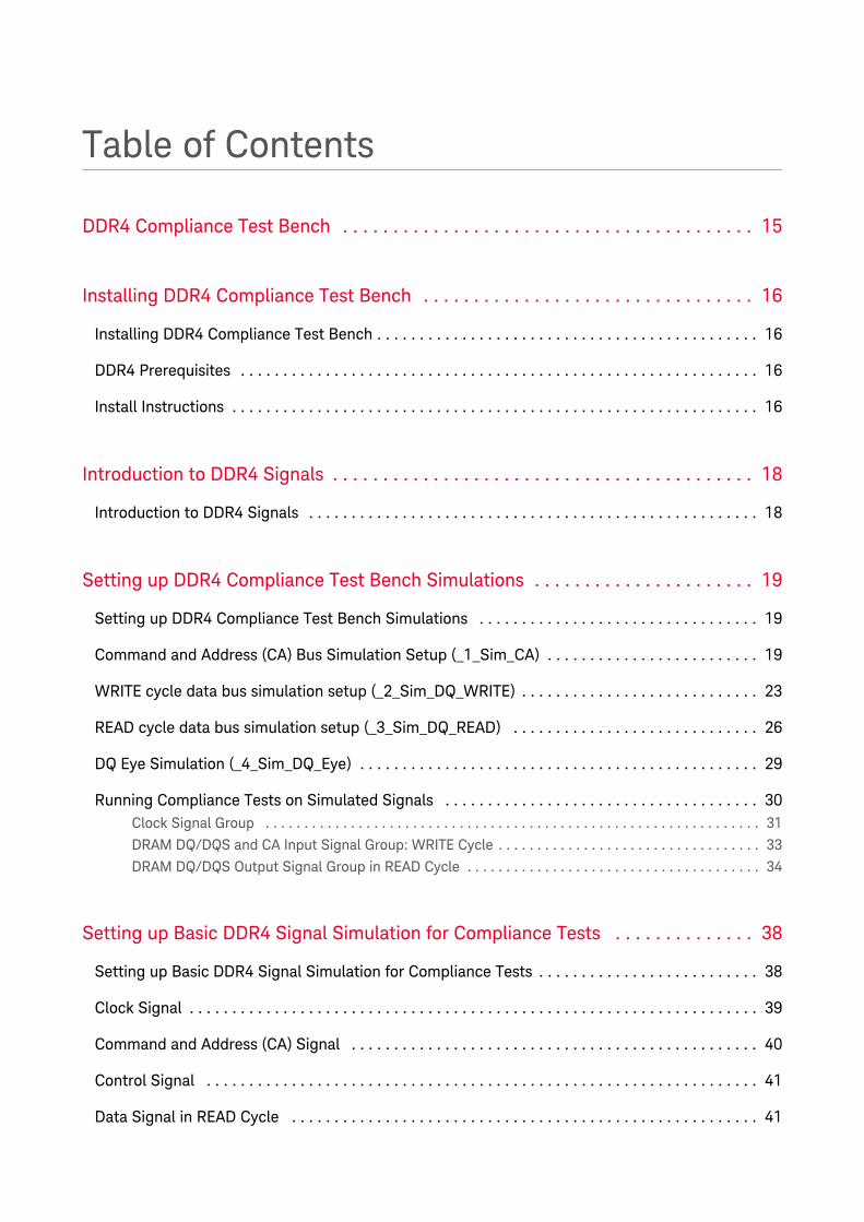
Table of Contents
DDR4 Compliance Test Bench . . . . . . . . . . . . . . . . . . . . . . . . . . . . . . . . . . . . . . . . . 15
Installing DDR4 Compliance Test Bench . . . . . . . . . . . . . . . . . . . . . . . . . . . . . . . . . 16
Installing DDR4 Compliance Test Bench . . . . . . . . . . . . . . . . . . . . . . . . . . . . . . . . . . . . . . . . . . . . . 16
DDR4 Prerequisites . . . . . . . . . . . . . . . . . . . . . . . . . . . . . . . . . . . . . . . . . . . . . . . . . . . . . . . . . . . . . 16
Install Instructions . . . . . . . . . . . . . . . . . . . . . . . . . . . . . . . . . . . . . . . . . . . . . . . . . . . . . . . . . . . . . . 16
Introduction to DDR4 Signals . . . . . . . . . . . . . . . . . . . . . . . . . . . . . . . . . . . . . . . . . . 18
Introduction to DDR4 Signals . . . . . . . . . . . . . . . . . . . . . . . . . . . . . . . . . . . . . . . . . . . . . . . . . . . . . 18
Setting up DDR4 Compliance Test Bench Simulations . . . . . . . . . . . . . . . . . . . . . . 19
Setting up DDR4 Compliance Test Bench Simulations . . . . . . . . . . . . . . . . . . . . . . . . . . . . . . . . . 19
Command and Address (CA) Bus Simulation Setup (_1_Sim_CA) . . . . . . . . . . . . . . . . . . . . . . . . . 19
WRITE cycle data bus simulation setup (_2_Sim_DQ_WRITE) . . . . . . . . . . . . . . . . . . . . . . . . . . . . 23
READ cycle data bus simulation setup (_3_Sim_DQ_READ) . . . . . . . . . . . . . . . . . . . . . . . . . . . . . 26
DQ Eye Simulation (_4_Sim_DQ_Eye) . . . . . . . . . . . . . . . . . . . . . . . . . . . . . . . . . . . . . . . . . . . . . . . 29
Running Compliance Tests on Simulated Signals . . . . . . . . . . . . . . . . . . . . . . . . . . . . . . . . . . . . . 30Clock Signal Group . . . . . . . . . . . . . . . . . . . . . . . . . . . . . . . . . . . . . . . . . . . . . . . . . . . . . . . . . . . . . . . . 31
DRAM DQ/DQS and CA Input Signal Group: WRITE Cycle . . . . . . . . . . . . . . . . . . . . . . . . . . . . . . . . . . 33
DRAM DQ/DQS Output Signal Group in READ Cycle . . . . . . . . . . . . . . . . . . . . . . . . . . . . . . . . . . . . . . 34
Setting up Basic DDR4 Signal Simulation for Compliance Tests . . . . . . . . . . . . . . 38
Setting up Basic DDR4 Signal Simulation for Compliance Tests . . . . . . . . . . . . . . . . . . . . . . . . . . 38
Clock Signal . . . . . . . . . . . . . . . . . . . . . . . . . . . . . . . . . . . . . . . . . . . . . . . . . . . . . . . . . . . . . . . . . . . 39
Command and Address (CA) Signal . . . . . . . . . . . . . . . . . . . . . . . . . . . . . . . . . . . . . . . . . . . . . . . . 40
Control Signal . . . . . . . . . . . . . . . . . . . . . . . . . . . . . . . . . . . . . . . . . . . . . . . . . . . . . . . . . . . . . . . . . 41
Data Signal in READ Cycle . . . . . . . . . . . . . . . . . . . . . . . . . . . . . . . . . . . . . . . . . . . . . . . . . . . . . . . 41
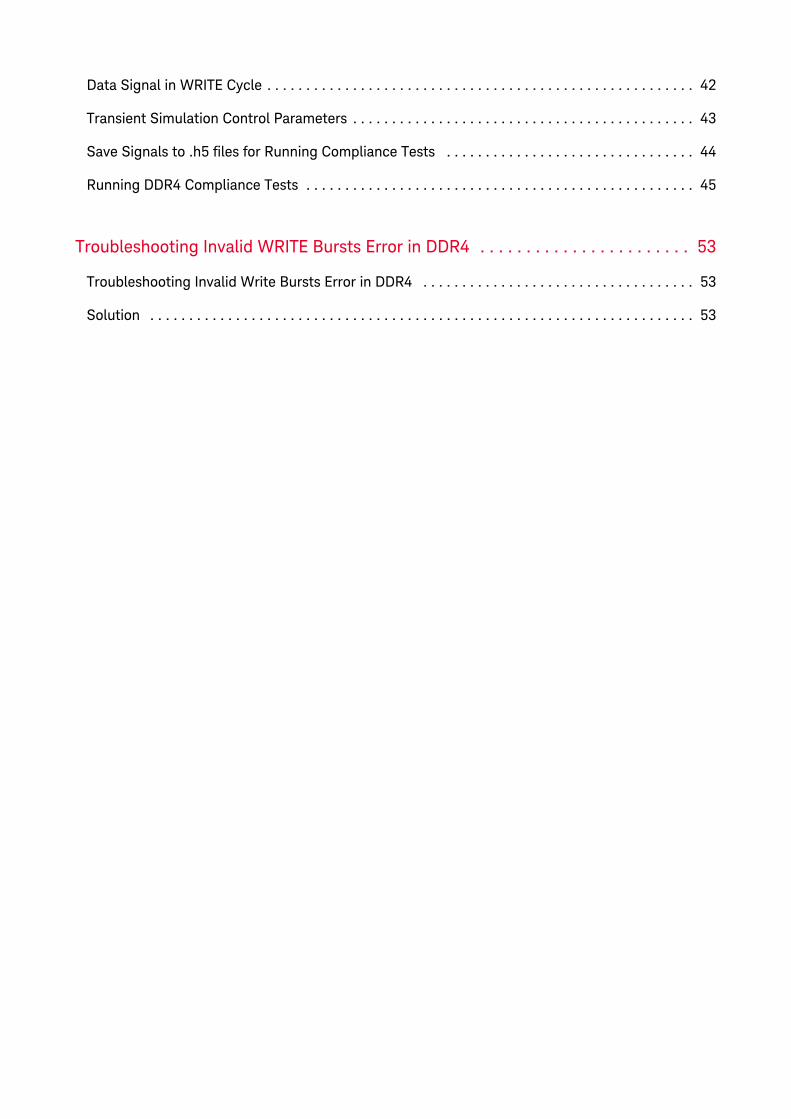
Data Signal in WRITE Cycle . . . . . . . . . . . . . . . . . . . . . . . . . . . . . . . . . . . . . . . . . . . . . . . . . . . . . . . 42
Transient Simulation Control Parameters . . . . . . . . . . . . . . . . . . . . . . . . . . . . . . . . . . . . . . . . . . . . 43
Save Signals to .h5 files for Running Compliance Tests . . . . . . . . . . . . . . . . . . . . . . . . . . . . . . . . 44
Running DDR4 Compliance Tests . . . . . . . . . . . . . . . . . . . . . . . . . . . . . . . . . . . . . . . . . . . . . . . . . . 45
Troubleshooting Invalid WRITE Bursts Error in DDR4 . . . . . . . . . . . . . . . . . . . . . . . 53
Troubleshooting Invalid Write Bursts Error in DDR4 . . . . . . . . . . . . . . . . . . . . . . . . . . . . . . . . . . . 53
Solution . . . . . . . . . . . . . . . . . . . . . . . . . . . . . . . . . . . . . . . . . . . . . . . . . . . . . . . . . . . . . . . . . . . . . . 53
DDR4 Compliance Test Bench
15
DDR4 Compliance Test BenchThis section describes the following topics:
Installing DDR4 Compliance Test Bench
Introduction to DDR4 Signals
Setting up Basic DDR4 Signal Simulation for Compliance Tests
Setting up DDR4 Compliance Test Bench Simulations
Troubleshooting Invalid WRITE Bursts Error in DDR4
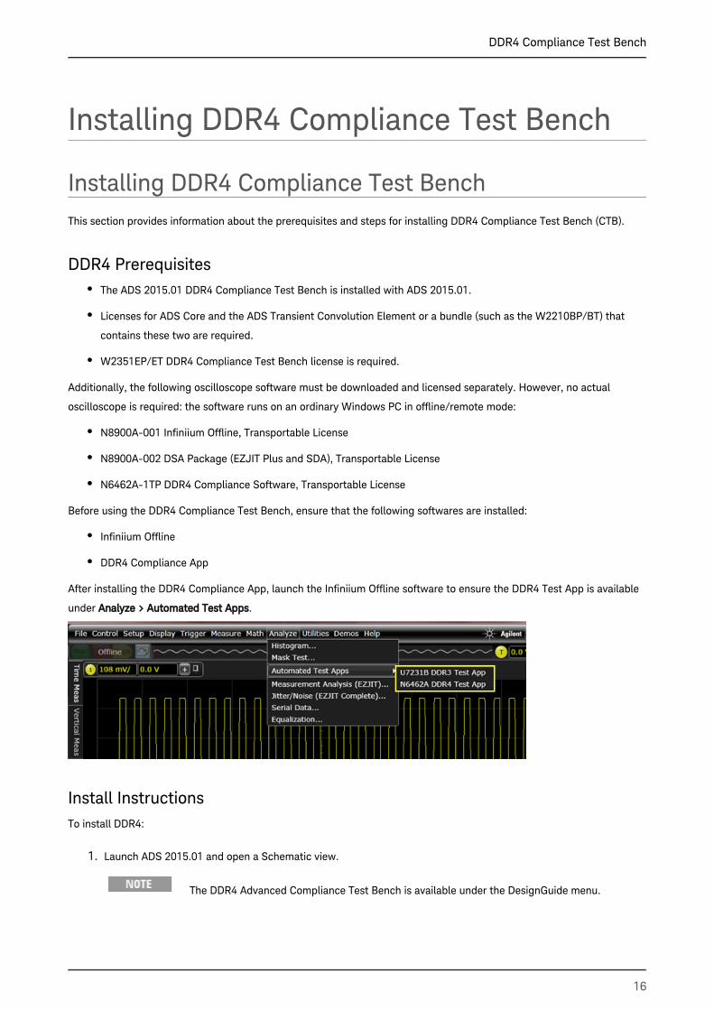
DDR4 Compliance Test Bench
16
1.
Installing DDR4 Compliance Test Bench
Installing DDR4 Compliance Test BenchThis section provides information about the prerequisites and steps for installing DDR4 Compliance Test Bench (CTB).
DDR4 PrerequisitesThe ADS 2015.01 DDR4 Compliance Test Bench is installed with ADS 2015.01.
Licenses for ADS Core and the ADS Transient Convolution Element or a bundle (such as the W2210BP/BT) that
contains these two are required.
W2351EP/ET DDR4 Compliance Test Bench license is required.
Additionally, the following oscilloscope software must be downloaded and licensed separately. However, no actual
oscilloscope is required: the software runs on an ordinary Windows PC in offline/remote mode:
N8900A-001 Infiniium Offline, Transportable License
N8900A-002 DSA Package (EZJIT Plus and SDA), Transportable License
N6462A-1TP DDR4 Compliance Software, Transportable License
Before using the DDR4 Compliance Test Bench, ensure that the following softwares are installed:
Infiniium Offline
DDR4 Compliance App
After installing the DDR4 Compliance App, launch the Infiniium Offline software to ensure the DDR4 Test App is available
under .Analyze > Automated Test Apps
Install InstructionsTo install DDR4:
Launch ADS 2015.01 and open a Schematic view.
The DDR4 Advanced Compliance Test Bench is available under the DesignGuide menu.
DDR4 Compliance Test Bench
17
2.
3.
4.
5.
Download the Infiniium Offline Oscilloscope Analysis Software from the Keysight website and follow the on-
screen installation instructions.
Close all the applications on your PC before installing the software.
Restart your PC to complete the installation.
Download the DDR4 Compliance Test Application Software from the Keysight website and follow the on-screen
installation instructions.
http://www.keysight.com/main/software.jspx?cc=IN&lc=eng&ckey=2229434&nid=-34333.1094284&id=2229434
Restart your PC after completing the installation.
DDR4 Compliance Test Bench
18
Introduction to DDR4 Signals
Introduction to DDR4 SignalsThere are 4 groups of signals in a typical DDR4 memory system:
Data group: DQS[7:0], DQSb[7:0], DQ[63:0]
Command and Address (CA) group: BA[2:0] (3 bits for 8 banks), A[15:0], command input including RAS#, CAS#,
WE#
Control group: Chip Select CS[3:0] (4 bits for 16 chips), Clock Enable CKE[3:0] (4 bits for 16 clocks pairs, ODT[3:0]
Clock group: CLK[3:0] and CLKb[3:0]
Following is a block diagram of a memory controller.
DDR4 Compliance Test Bench
19
1.
2.
3.
Setting up DDR4 Compliance Test Bench Simulations
Setting up DDR4 Compliance Test Bench SimulationsThis section describes the simulation setups of the following:
Command and Address Bus Simulation Setup
WRITE cycle data bus simulation setup
READ cycle data bus simulation setup
DQ Eye Simulation
Command and Address (CA) Bus Simulation Setup (_1_Sim_CA)In _1_Sim_CA, the following CA Bus topology simulation has been setup.
It is a simplified CA bus topology, with 6 singled-ended CA signals (CA0~CA5), 1 single-ended control signal (CS0 for
Chip Select), and 1 differential clock signal (+/-, CLK/CLKb).
The block on the left side is a pattern generator:
CA0~CA5 are generating pseudo-random bit patterns at a rate equal to the data rate. The reason for this bit rate
is that column and row address signals are multiplexed to the same address line. As a result, the address bus is
running the same bit rate as that on the data bus.
CLK_0101 is generating a repetitive 0101 bit pattern at the same rate as CA0~CA5
CS0 is generating a pseudo-random bit pattern at a ½ the rate of CA0~CA5.
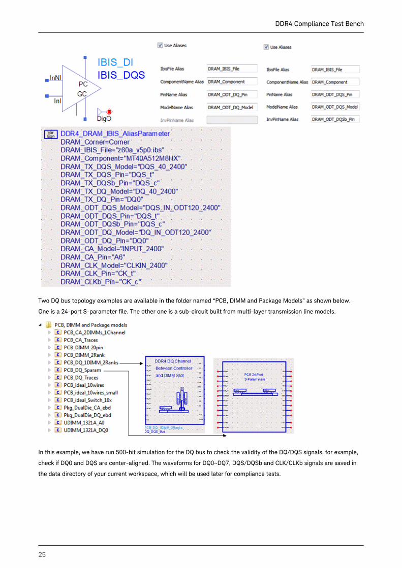
The CA_Driver and CA_Receiver blocks contain I/O buffer models referencing the same IBIS file. In practice, you should
get at least 2 IBIS files, one from your DRAM vendor (e.g., Micron) for the DRAM I/O, and another one from your
processor vendor (e.g., Intel) for the controller I/O. This example uses only one IBIS file from Micron for the DRAM I/O. It
uses a DRAM DQ pin driver model, as if it were the controller CA pin driver, to drive the CA bus. Following screenshot
shows how the CA Pin driver and receiver models are set up using alias names:
DDR4 Compliance Test Bench
20
CA and CLK Driver Pin
CA Receiver Pin
CS0 Receiver Pin
CLK/CLKb Receiver Pin
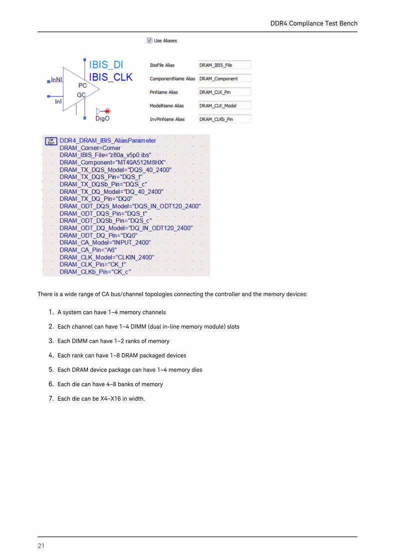
DDR4 Compliance Test Bench
21
1.
2.
3.
4.
5.
6.
7.
There is a wide range of CA bus/channel topologies connecting the controller and the memory devices:
A system can have 1~4 memory channels
Each channel can have 1~4 DIMM (dual in-line memory module) slots
Each DIMM can have 1~2 ranks of memory
Each rank can have 1~8 DRAM packaged devices
Each DRAM device package can have 1~4 memory dies
Each die can have 4~8 banks of memory
Each die can be X4~X16 in width.
DDR4 Compliance Test Bench
22
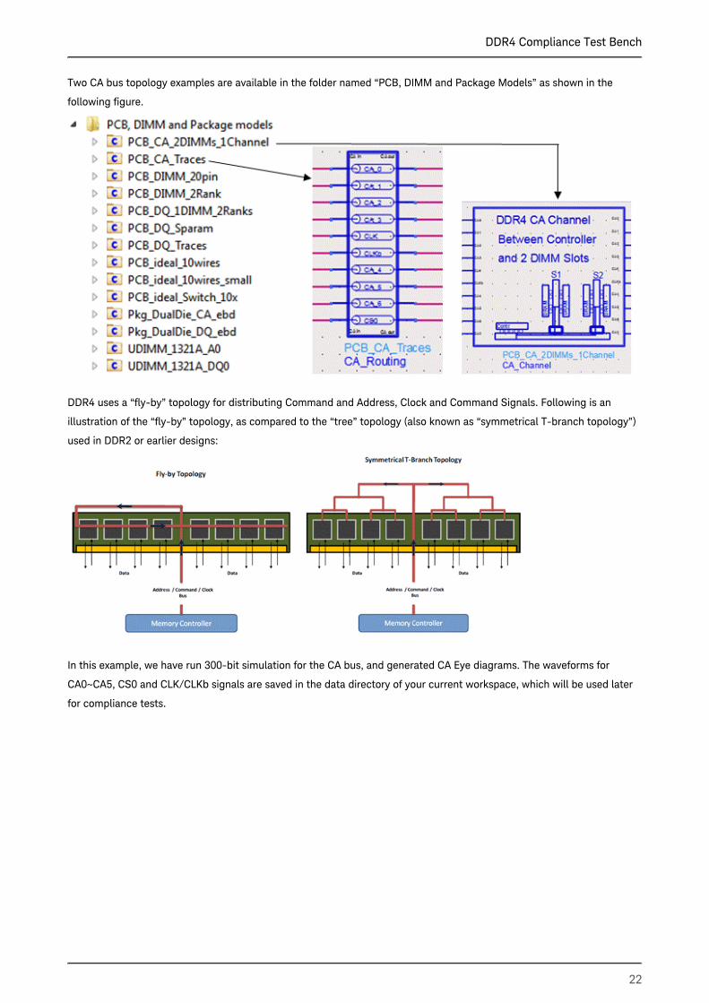
Two CA bus topology examples are available in the folder named “PCB, DIMM and Package Models” as shown in the
following figure.
DDR4 uses a “fly-by” topology for distributing Command and Address, Clock and Command Signals. Following is an
illustration of the “fly-by” topology, as compared to the “tree” topology (also known as “symmetrical T-branch topology”)
used in DDR2 or earlier designs:
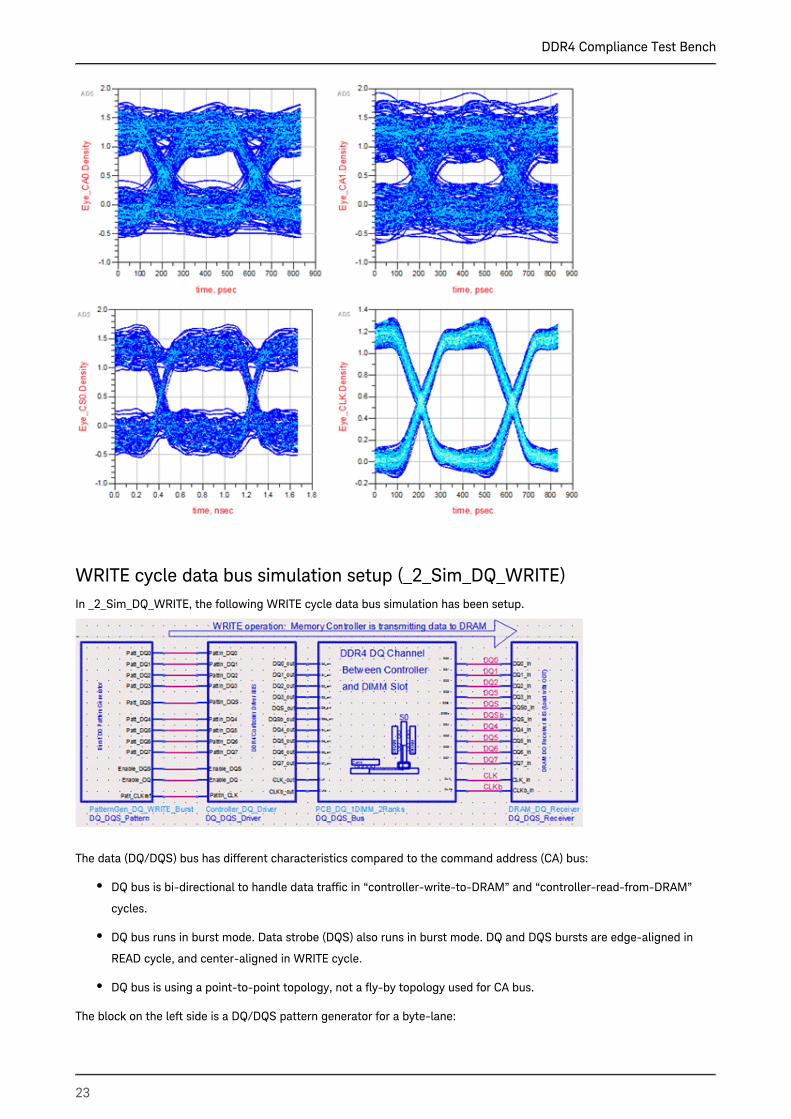
In this example, we have run 300-bit simulation for the CA bus, and generated CA Eye diagrams. The waveforms for
CA0~CA5, CS0 and CLK/CLKb signals are saved in the data directory of your current workspace, which will be used later
for compliance tests.
DDR4 Compliance Test Bench
23
WRITE cycle data bus simulation setup (_2_Sim_DQ_WRITE)In _2_Sim_DQ_WRITE, the following WRITE cycle data bus simulation has been setup.
The data (DQ/DQS) bus has different characteristics compared to the command address (CA) bus:
DQ bus is bi-directional to handle data traffic in “controller-write-to-DRAM” and “controller-read-from-DRAM”
cycles.
DQ bus runs in burst mode. Data strobe (DQS) also runs in burst mode. DQ and DQS bursts are edge-aligned in
READ cycle, and center-aligned in WRITE cycle.
DQ bus is using a point-to-point topology, not a fly-by topology used for CA bus.
The block on the left side is a DQ/DQS pattern generator for a byte-lane:
DDR4 Compliance Test Bench
24
1.
2.
3.
4.
5.
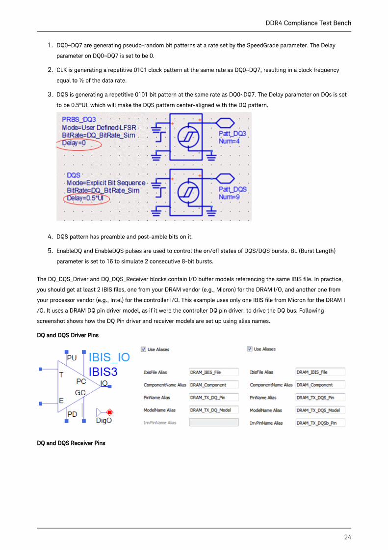
DQ0~DQ7 are generating pseudo-random bit patterns at a rate set by the SpeedGrade parameter. The Delay
parameter on DQ0~DQ7 is set to be 0.
CLK is generating a repetitive 0101 clock pattern at the same rate as DQ0~DQ7, resulting in a clock frequency
equal to ½ of the data rate.
DQS is generating a repetitive 0101 bit pattern at the same rate as DQ0~DQ7. The Delay parameter on DQs is set
to be 0.5*UI, which will make the DQS pattern center-aligned with the DQ pattern.
DQS pattern has preamble and post-amble bits on it.
EnableDQ and EnableDQS pulses are used to control the on/off states of DQS/DQS bursts. BL (Burst Length)
parameter is set to 16 to simulate 2 consecutive 8-bit bursts.
The DQ_DQS_Driver and DQ_DQS_Receiver blocks contain I/O buffer models referencing the same IBIS file. In practice,
you should get at least 2 IBIS files, one from your DRAM vendor (e.g., Micron) for the DRAM I/O, and another one from
your processor vendor (e.g., Intel) for the controller I/O. This example uses only one IBIS file from Micron for the DRAM I
/O. It uses a DRAM DQ pin driver model, as if it were the controller DQ pin driver, to drive the DQ bus. Following
screenshot shows how the DQ Pin driver and receiver models are set up using alias names.
DQ and DQS Driver Pins
DQ and DQS Receiver Pins
DDR4 Compliance Test Bench
25
Two DQ bus topology examples are available in the folder named “PCB, DIMM and Package Models” as shown below.
One is a 24-port S-parameter file. The other one is a sub-circuit built from multi-layer transmission line models.
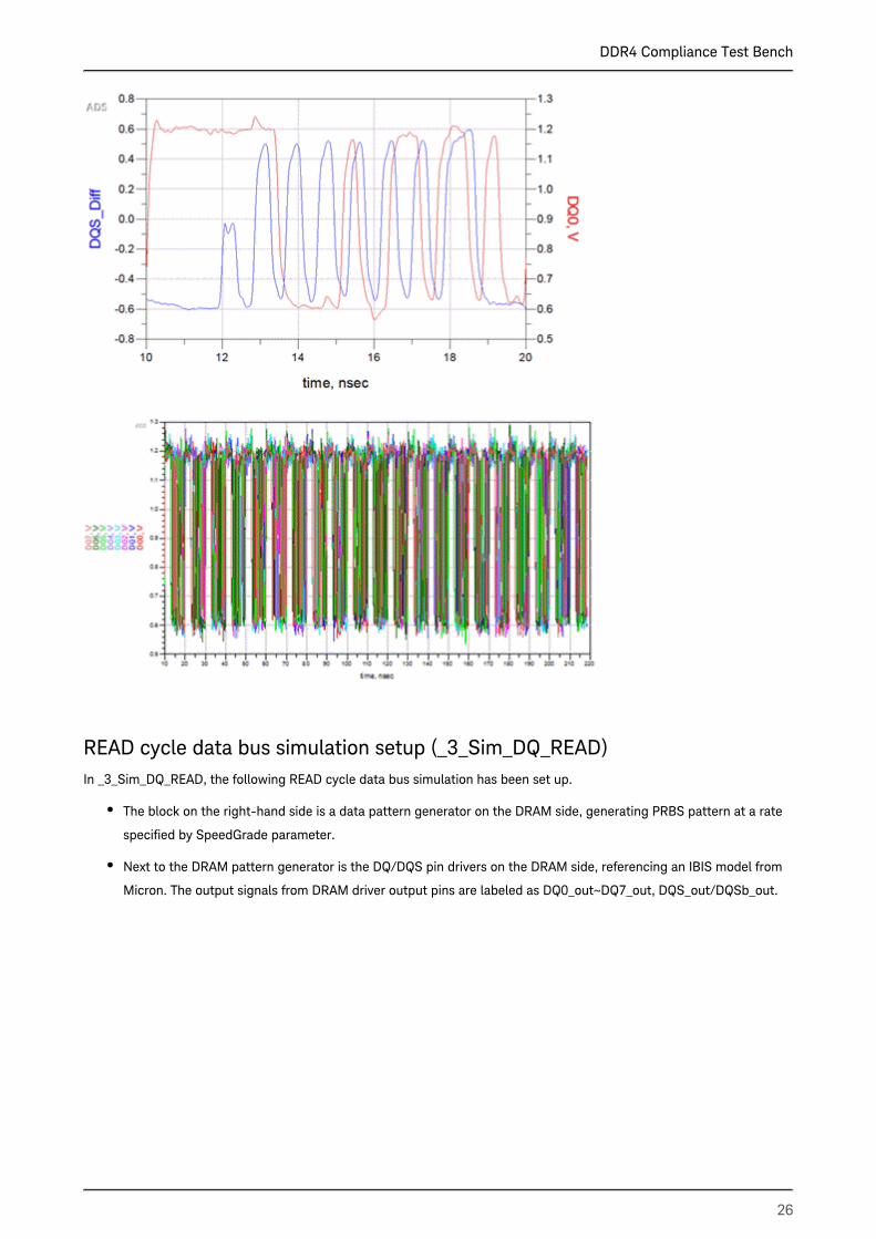
In this example, we have run 500-bit simulation for the DQ bus to check the validity of the DQ/DQS signals, for example,
check if DQ0 and DQS are center-aligned. The waveforms for DQ0~DQ7, DQS/DQSb and CLK/CLKb signals are saved in
the data directory of your current workspace, which will be used later for compliance tests.
DDR4 Compliance Test Bench
26
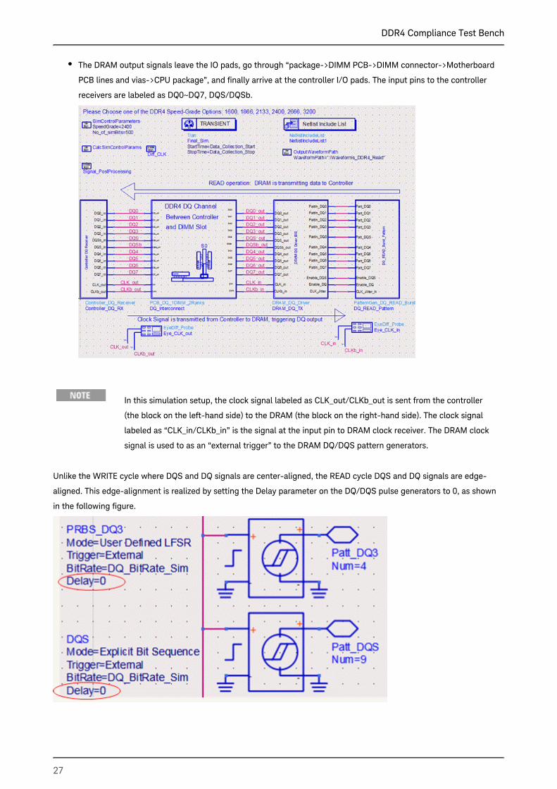
READ cycle data bus simulation setup (_3_Sim_DQ_READ)In _3_Sim_DQ_READ, the following READ cycle data bus simulation has been set up.
The block on the right-hand side is a data pattern generator on the DRAM side, generating PRBS pattern at a rate
specified by SpeedGrade parameter.
Next to the DRAM pattern generator is the DQ/DQS pin drivers on the DRAM side, referencing an IBIS model from
Micron. The output signals from DRAM driver output pins are labeled as DQ0_out~DQ7_out, DQS_out/DQSb_out.
DDR4 Compliance Test Bench
27
The DRAM output signals leave the IO pads, go through “package->DIMM PCB->DIMM connector->Motherboard
PCB lines and vias->CPU package”, and finally arrive at the controller I/O pads. The input pins to the controller
receivers are labeled as DQ0~DQ7, DQS/DQSb.
In this simulation setup, the clock signal labeled as CLK_out/CLKb_out is sent from the controller
(the block on the left-hand side) to the DRAM (the block on the right-hand side). The clock signal
labeled as “CLK_in/CLKb_in” is the signal at the input pin to DRAM clock receiver. The DRAM clock
signal is used to as an “external trigger” to the DRAM DQ/DQS pattern generators.
Unlike the WRITE cycle where DQS and DQ signals are center-aligned, the READ cycle DQS and DQ signals are edge-
aligned. This edge-alignment is realized by setting the Delay parameter on the DQ/DQS pulse generators to 0, as shown
in the following figure.
DDR4 Compliance Test Bench
28
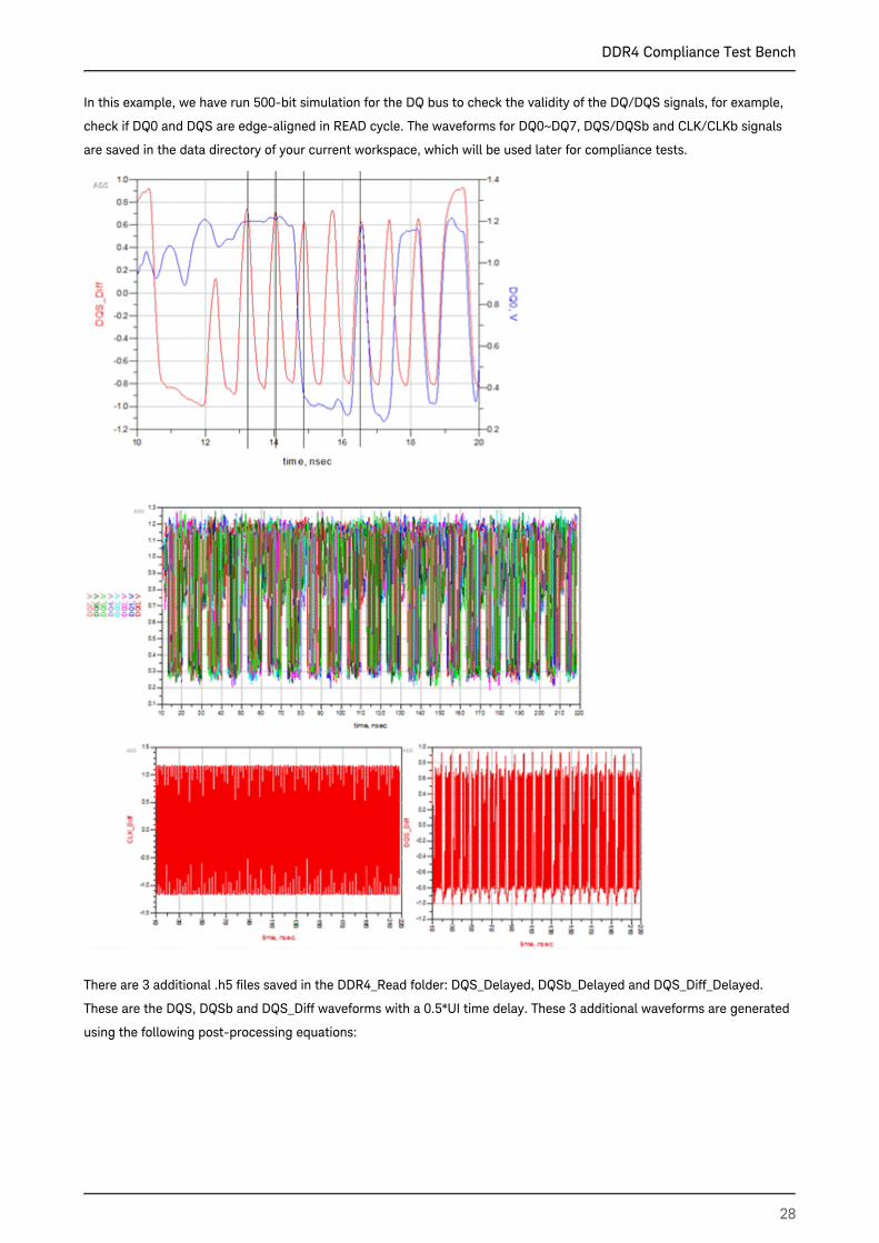
In this example, we have run 500-bit simulation for the DQ bus to check the validity of the DQ/DQS signals, for example,
check if DQ0 and DQS are edge-aligned in READ cycle. The waveforms for DQ0~DQ7, DQS/DQSb and CLK/CLKb signals
are saved in the data directory of your current workspace, which will be used later for compliance tests.
There are 3 additional .h5 files saved in the DDR4_Read folder: DQS_Delayed, DQSb_Delayed and DQS_Diff_Delayed.
These are the DQS, DQSb and DQS_Diff waveforms with a 0.5*UI time delay. These 3 additional waveforms are generated
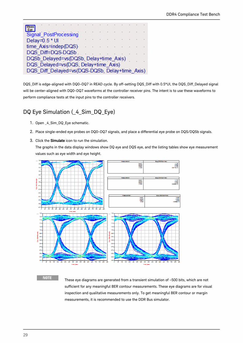
using the following post-processing equations:
DDR4 Compliance Test Bench
29
1.
2.
3.
DQS_Diff is edge-aligned with DQ0~DQ7 in READ cycle. By off-setting DQS_Diff with 0.5*UI, the DQS_Diff_Delayed signal
will be center-aligned with DQ0~DQ7 waveforms at the controller receiver pins. The intent is to use these waveforms to
perform compliance tests at the input pins to the controller receivers.
DQ Eye Simulation (_4_Sim_DQ_Eye)
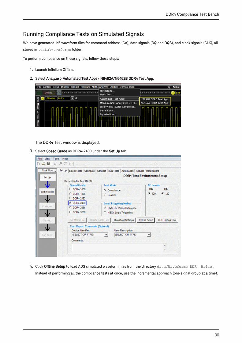
Open _4_Sim_DQ_Eye schematic.
Place single-ended eye probes on DQ0~DQ7 signals, and place a differential eye probe on DQS/DQSb signals.
Click the icon to run the simulation.Simulate
The graphs in the data display windows show DQ eye and DQS eye, and the listing tables show eye measurement
values such as eye width and eye height.
These eye diagrams are generated from a transient simulation of ~500 bits, which are not
sufficient for any meaningful BER contour measurements. These eye diagrams are for visual
inspection and qualitative measurements only. To get meaningful BER contour or margin
measurements, it is recommended to use the DDR Bus simulator.
DDR4 Compliance Test Bench
30
1.
2.
3.
4.
Running Compliance Tests on Simulated SignalsWe have generated .h5 waveform files for command address (CA), data signals (DQ and DQS), and clock signals (CLK), all
stored in folder..data\waveforms
To perform compliance on these signals, follow these steps:
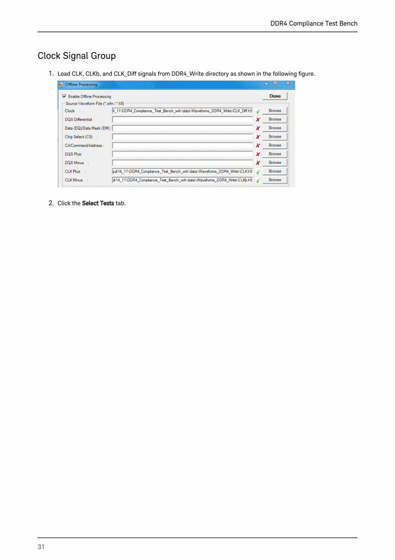
Launch Infiniium Offline.
Select .Analyze > Automated Test Apps> N6462A/N6462B DDR4 Test App
The DDR4 Test window is displayed.
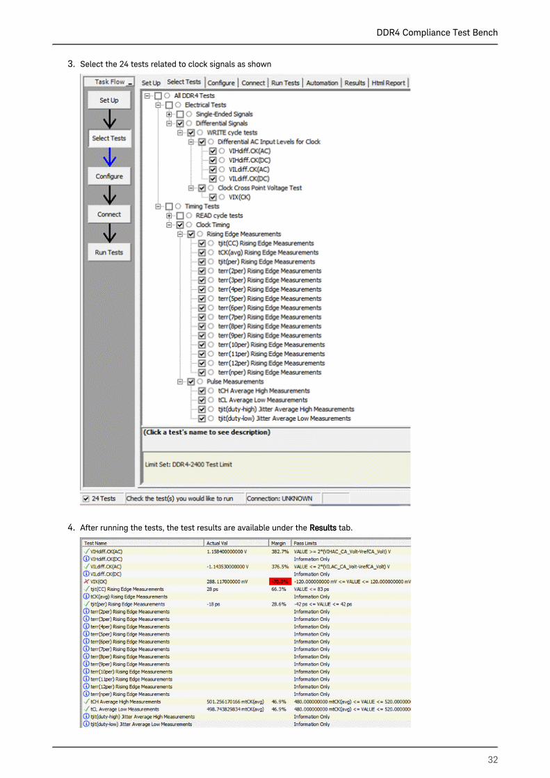
Select as DDR4-2400 under the tab.Speed Grade Set Up
Click to load ADS simulated waveform files from the directory Offline Setup data/Waveforms_DDR4_Write.
Instead of performing all the compliance tests at once, use the incremental approach (one signal group at a time).
DDR4 Compliance Test Bench
31
1.
2.
Clock Signal Group
Load CLK, CLKb, and CLK_Diff signals from DDR4_Write directory as shown in the following figure.
Click the tab.Select Tests
DDR4 Compliance Test Bench
32
3.
4.
Select the 24 tests related to clock signals as shown
After running the tests, the test results are available under the tab. Results
DDR4 Compliance Test Bench
33
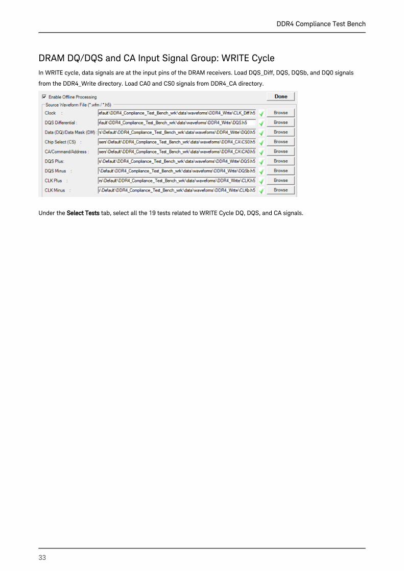
DRAM DQ/DQS and CA Input Signal Group: WRITE CycleIn WRITE cycle, data signals are at the input pins of the DRAM receivers. Load DQS_Diff, DQS, DQSb, and DQ0 signals
from the DDR4_Write directory. Load CA0 and CS0 signals from DDR4_CA directory.
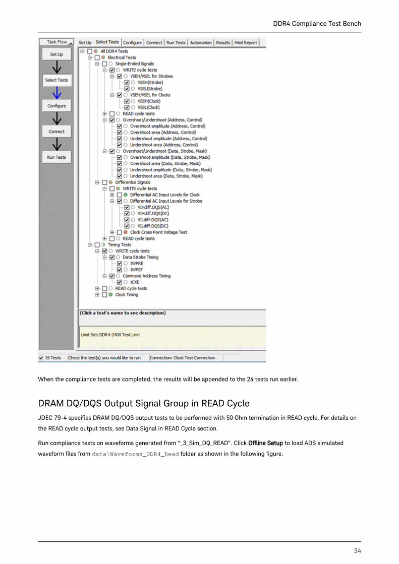
Under the tab, select all the 19 tests related to WRITE Cycle DQ, DQS, and CA signals.Select Tests
DDR4 Compliance Test Bench
34
When the compliance tests are completed, the results will be appended to the 24 tests run earlier.
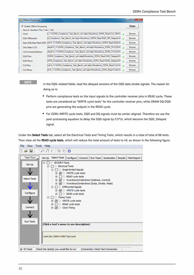
DRAM DQ/DQS Output Signal Group in READ CycleJDEC 79-4 specifies DRAM DQ/DQS output tests to be performed with 50 Ohm termination in READ cycle. For details on
the READ cycle output tests, see Data Signal in READ Cycle section.
Run compliance tests on waveforms generated from “_3_Sim_DQ_READ”. Click to load ADS simulated Offline Setup
waveform files from folder as shown in the following figure.data\Waveforms_DDR4_Read
DDR4 Compliance Test Bench
35
In the DQS-related fields, load the delayed versions of the DQS data strobe signals. The reason for
doing so is:
Perform compliance tests on the input signals to the controller receiver pins in READ cycle. These
tests are considered as “WRITE cycle tests” for the controller receiver pins, while DRAM DQ/DQS
pins are generating the outputs in the READ cycle.
For DDR4 WRITE cycle tests, DQS and DQ signals must be center-aligned. Therefore we use the
post-processing equation to delay the DQS signal by 0.5*UI, which become the DQS_Delayed
signal.
Under the tab, select all the Electrical Tests and Timing Tests, which results in a total of total of 66 tests. Select Tests
Then clear all the , which will reduce the total amount of tests to 43, as shown in the following figure.READ cycle tests
DDR4 Compliance Test Bench
36
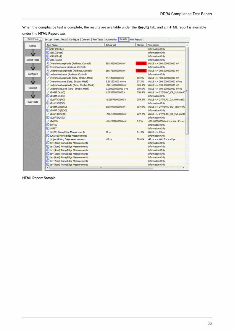
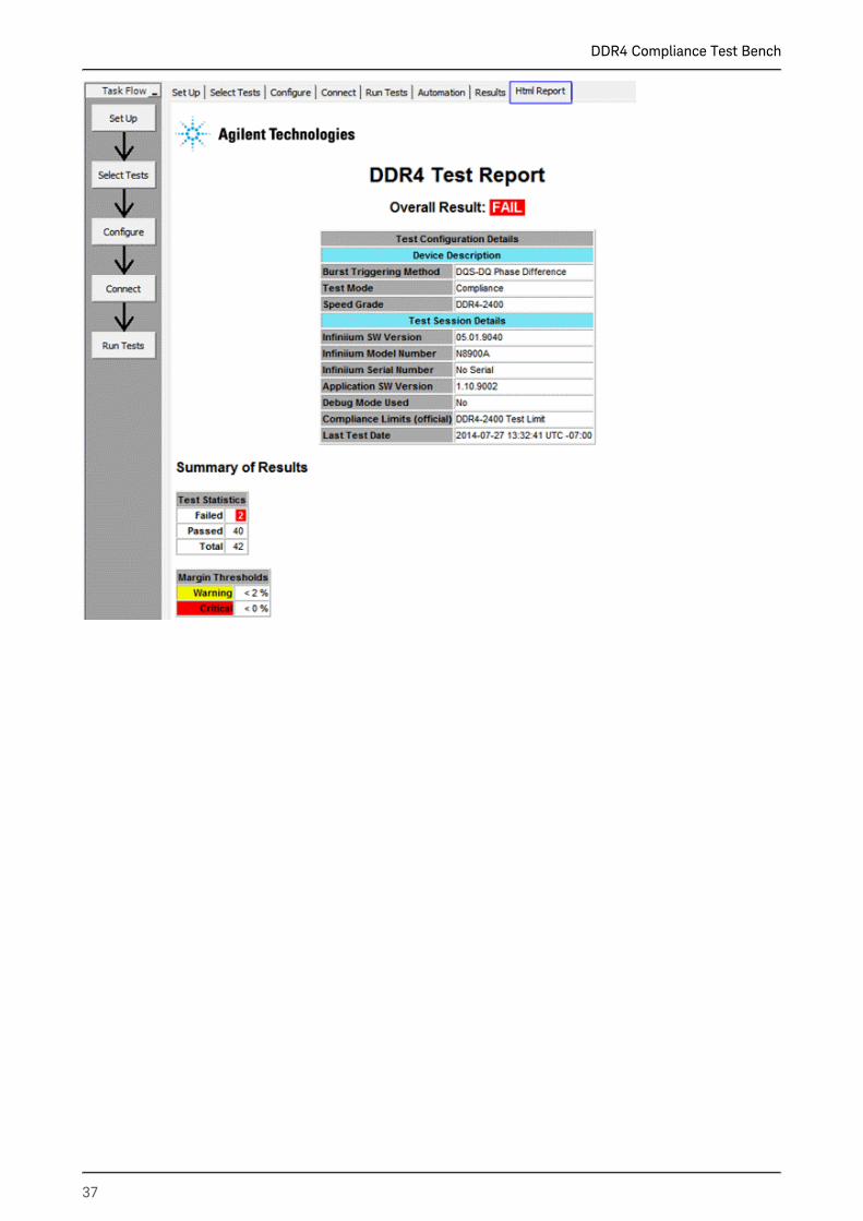
When the compliance test is complete, the results are available under the tab, and an HTML report is available Results
under the tab. HTML Report
HTML Report Sample
DDR4 Compliance Test Bench
37
DDR4 Compliance Test Bench
38
Setting up Basic DDR4 Signal Simulation for Compliance Tests
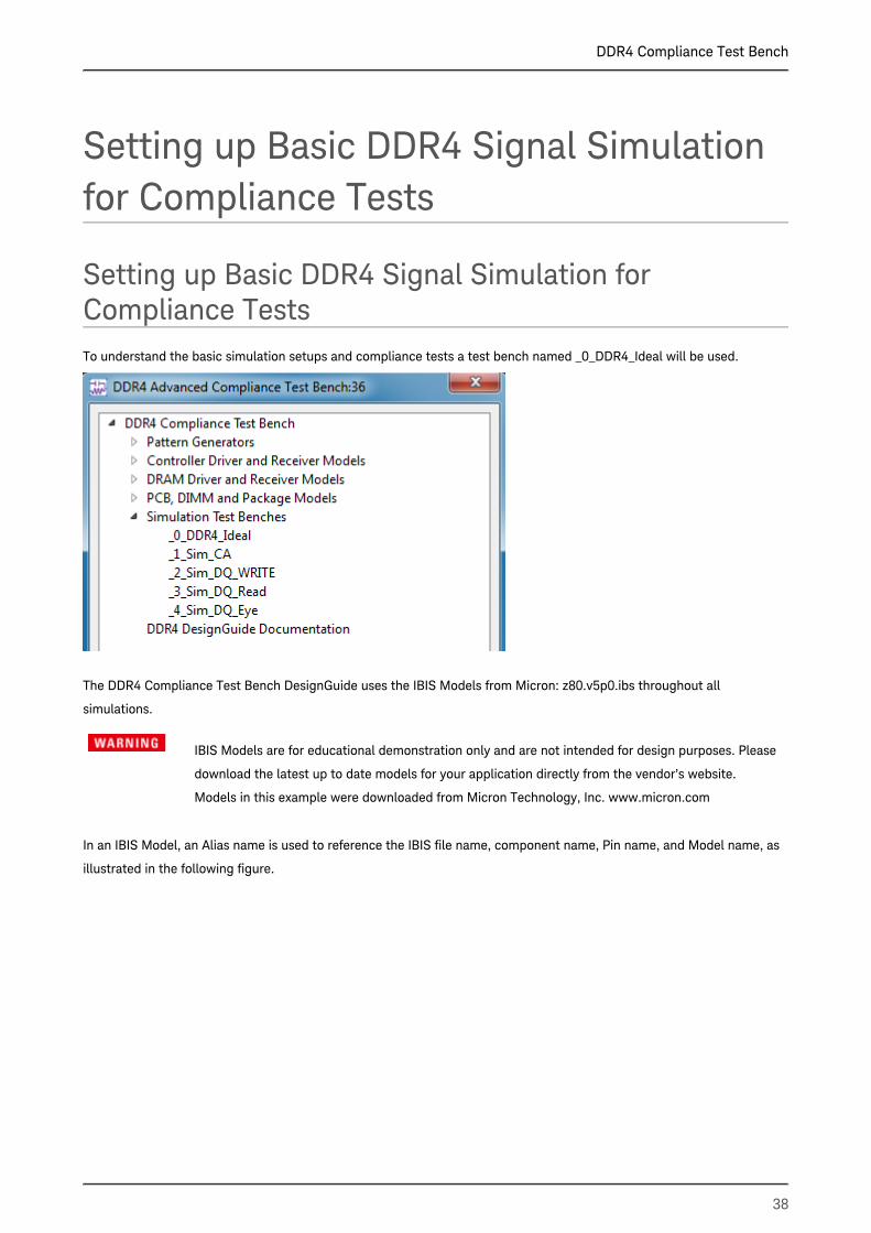
Setting up Basic DDR4 Signal Simulation for Compliance TestsTo understand the basic simulation setups and compliance tests a test bench named _0_DDR4_Ideal will be used.
The DDR4 Compliance Test Bench DesignGuide uses the IBIS Models from Micron: z80.v5p0.ibs throughout all
simulations.
IBIS Models are for educational demonstration only and are not intended for design purposes. Please
download the latest up to date models for your application directly from the vendor’s website.
Models in this example were downloaded from Micron Technology, Inc. www.micron.com
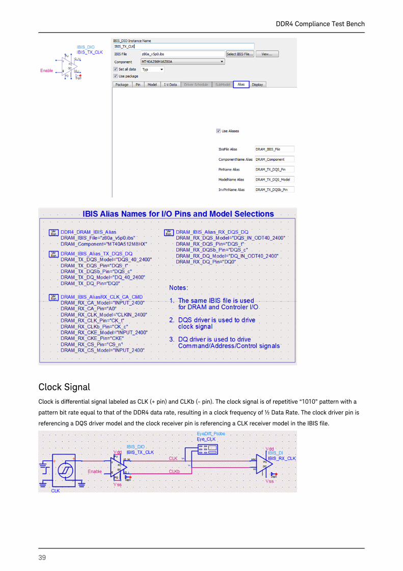
In an IBIS Model, an Alias name is used to reference the IBIS file name, component name, Pin name, and Model name, as
illustrated in the following figure.
DDR4 Compliance Test Bench
39
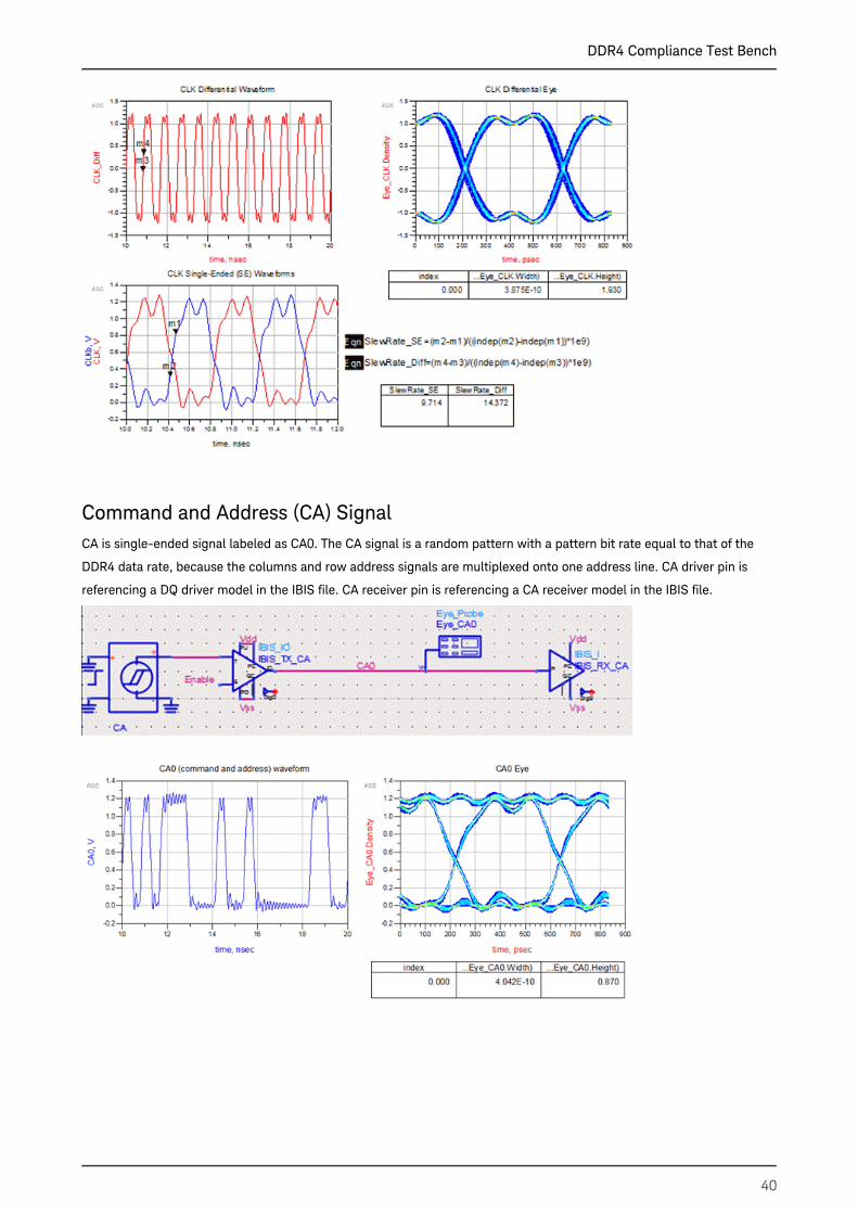
Clock SignalClock is differential signal labeled as CLK (+ pin) and CLKb (- pin). The clock signal is of repetitive “1010” pattern with a
pattern bit rate equal to that of the DDR4 data rate, resulting in a clock frequency of ½ Data Rate. The clock driver pin is
referencing a DQS driver model and the clock receiver pin is referencing a CLK receiver model in the IBIS file.
DDR4 Compliance Test Bench
40
Command and Address (CA) SignalCA is single-ended signal labeled as CA0. The CA signal is a random pattern with a pattern bit rate equal to that of the
DDR4 data rate, because the columns and row address signals are multiplexed onto one address line. CA driver pin is
referencing a DQ driver model in the IBIS file. CA receiver pin is referencing a CA receiver model in the IBIS file.
DDR4 Compliance Test Bench
41
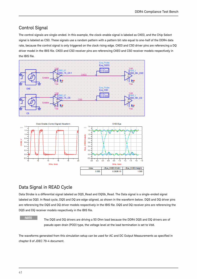
Control SignalThe control signals are single-ended. In this example, the clock-enable signal is labeled as CKE0, and the Chip Select
signal is labeled as CS0. These signals use a random pattern with a pattern bit rate equal to one-half of the DDR4 data
rate, because the control signal is only triggered on the clock rising edge. CKE0 and CS0 driver pins are referencing a DQ
driver model in the IBIS file. CKE0 and CS0 receiver pins are referencing CKE0 and CS0 receiver models respectively in
the IBIS file.
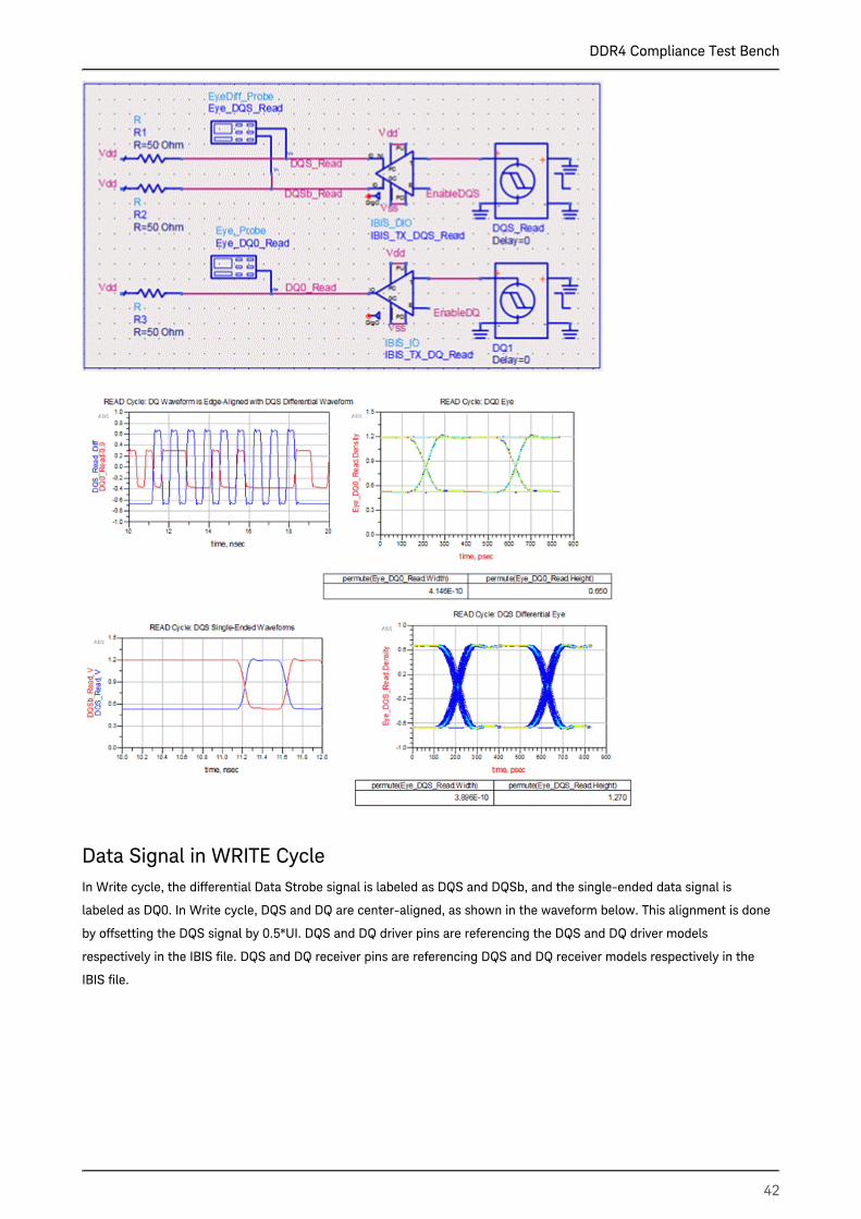
Data Signal in READ CycleData Strobe is a differential signal labeled as DQS_Read and DQSb_Read. The Data signal is a single-ended signal
labeled as DQ0. In Read cycle, DQS and DQ are edge-aligned, as shown in the waveform below. DQS and DQ driver pins
are referencing the DQS and DQ driver models respectively in the IBIS file. DQS and DQ receiver pins are referencing the
DQS and DQ receiver models respectively in the IBIS file.
The DQS and DQ drivers are driving a 50 Ohm load because the DDR4 DQS and DQ drivers are of
pseudo open drain (POD) type, the voltage level at the load termination is set to Vdd.
The waveforms generated from this simulation setup can be used for AC and DC Output Measurements as specified in
chapter 8 of JDEC 79-4 document.
DDR4 Compliance Test Bench
42
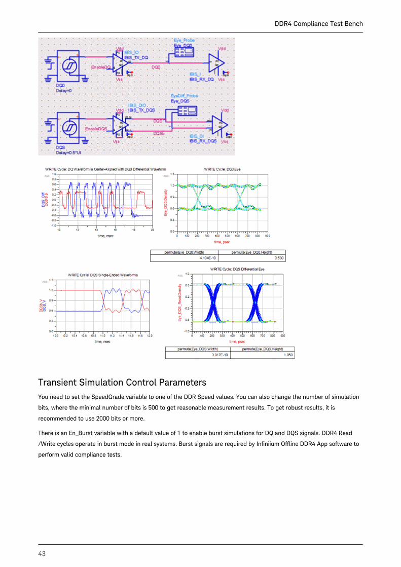
Data Signal in WRITE CycleIn Write cycle, the differential Data Strobe signal is labeled as DQS and DQSb, and the single-ended data signal is
labeled as DQ0. In Write cycle, DQS and DQ are center-aligned, as shown in the waveform below. This alignment is done
by offsetting the DQS signal by 0.5*UI. DQS and DQ driver pins are referencing the DQS and DQ driver models
respectively in the IBIS file. DQS and DQ receiver pins are referencing DQS and DQ receiver models respectively in the
IBIS file.
DDR4 Compliance Test Bench
43
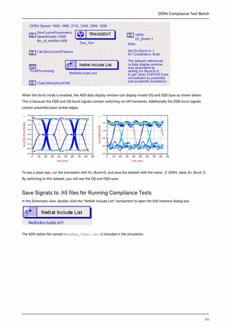
Transient Simulation Control ParametersYou need to set the SpeedGrade variable to one of the DDR Speed values. You can also change the number of simulation
bits, where the minimal number of bits is 500 to get reasonable measurement results. To get robust results, it is
recommended to use 2000 bits or more.
There is an En_Burst variable with a default value of 1 to enable burst simulations for DQ and DQS signals. DDR4 Read
/Write cycles operate in burst mode in real systems. Burst signals are required by Infiniium Offline DDR4 App software to
perform valid compliance tests.
DDR4 Compliance Test Bench
44
When the burst mode is enabled, the ADS data display window can display invalid DQ and DQS Eyes as shown below.
This is because the DQS and DQ burst signals contain switching-on/off transients. Additionally the DQS burst signals
contain preamble/post-amble edges.
To see a clean eye, run the simulation with En_Burst=0, and save the dataset with the name _0_DDR4_Ideal_En_Burst_0.
By switching to this dataset, you will see the DQ and DQS eyes.
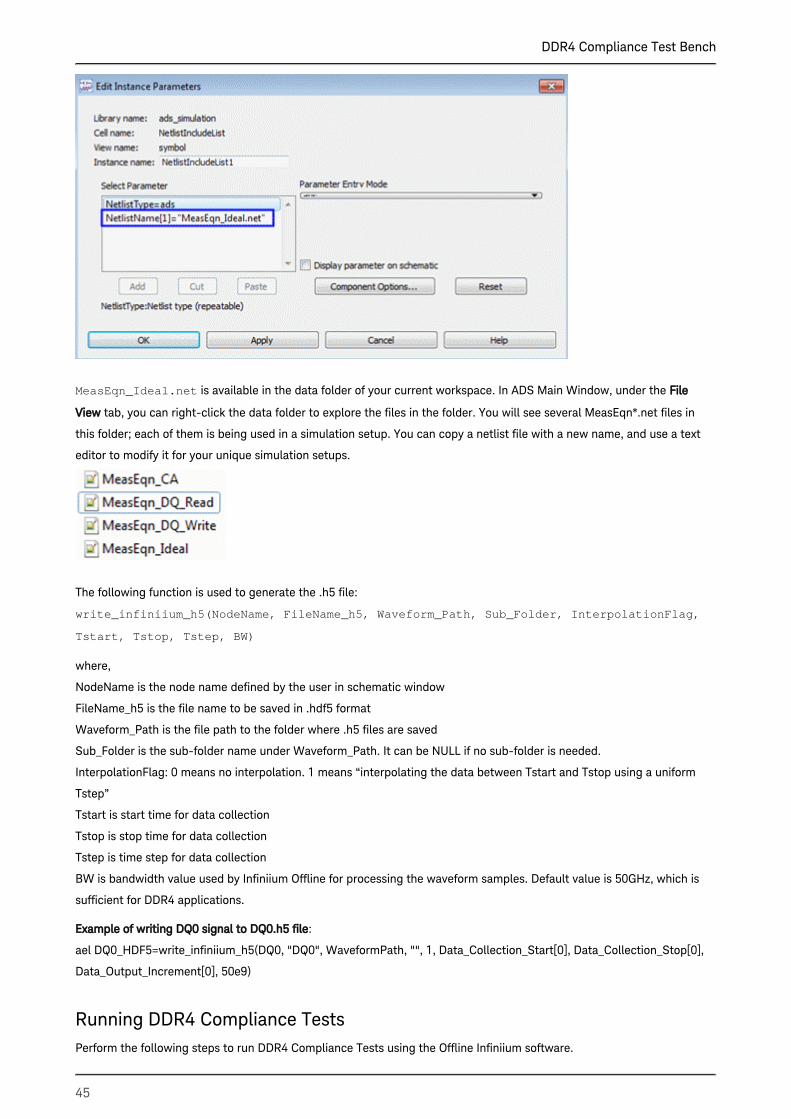
Save Signals to .h5 files for Running Compliance TestsIn the Schematic view, double-click the “Netlist Include List” component to open the Edit Instance dialog box.
The ADS netlist file named is included in the simulation.MeasEqn_Ideal.net
DDR4 Compliance Test Bench
45
MeasEqn_Ideal.net is available in the data folder of your current workspace. In ADS Main Window, under the File
tab, you can right-click the data folder to explore the files in the folder. You will see several MeasEqn*.net files in View
this folder; each of them is being used in a simulation setup. You can copy a netlist file with a new name, and use a text
editor to modify it for your unique simulation setups.
The following function is used to generate the .h5 file:
write_infiniium_h5(NodeName, FileName_h5, Waveform_Path, Sub_Folder, InterpolationFlag,
Tstart, Tstop, Tstep, BW)
where,
NodeName is the node name defined by the user in schematic window
FileName_h5 is the file name to be saved in .hdf5 format
Waveform_Path is the file path to the folder where .h5 files are saved
Sub_Folder is the sub-folder name under Waveform_Path. It can be NULL if no sub-folder is needed.
InterpolationFlag: 0 means no interpolation. 1 means “interpolating the data between Tstart and Tstop using a uniform
Tstep”
Tstart is start time for data collection
Tstop is stop time for data collection
Tstep is time step for data collection
BW is bandwidth value used by Infiniium Offline for processing the waveform samples. Default value is 50GHz, which is
sufficient for DDR4 applications.
Example of writing DQ0 signal to DQ0.h5 file:
ael DQ0_HDF5=write_infiniium_h5(DQ0, "DQ0", WaveformPath, "", 1, Data_Collection_Start[0], Data_Collection_Stop[0],
Data_Output_Increment[0], 50e9)
Running DDR4 Compliance TestsPerform the following steps to run DDR4 Compliance Tests using the Offline Infiniium software.
DDR4 Compliance Test Bench
46
1.
2.
3.
4.
5.
6.
7.
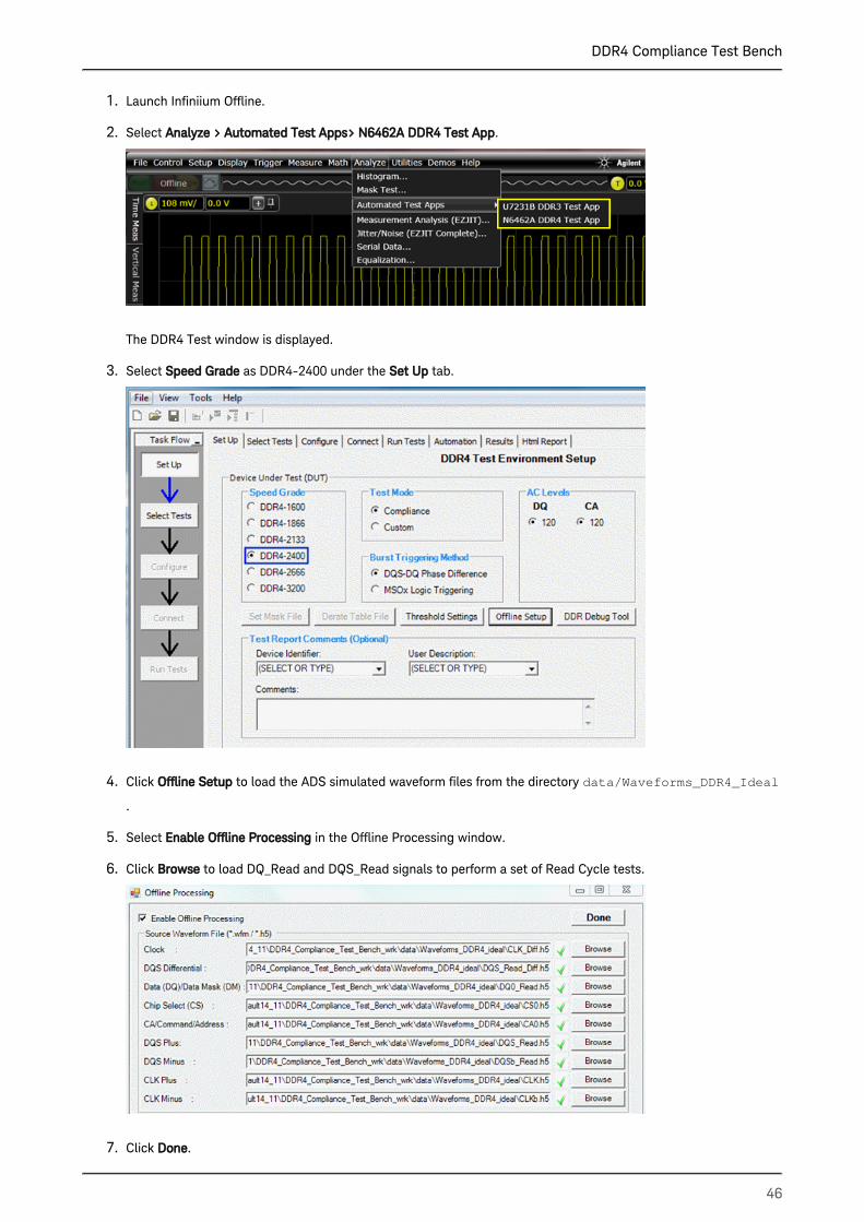
Launch Infiniium Offline.
Select .Analyze > Automated Test Apps> N6462A DDR4 Test App
The DDR4 Test window is displayed.
Select as DDR4-2400 under the tab.Speed Grade Set Up
Click to load the ADS simulated waveform files from the directory Offline Setup data/Waveforms_DDR4_Ideal
.
Select in the Offline Processing window.Enable Offline Processing
Click to load DQ_Read and DQS_Read signals to perform a set of Read Cycle tests.Browse
Click .Done
DDR4 Compliance Test Bench
47
8.
a.
b.
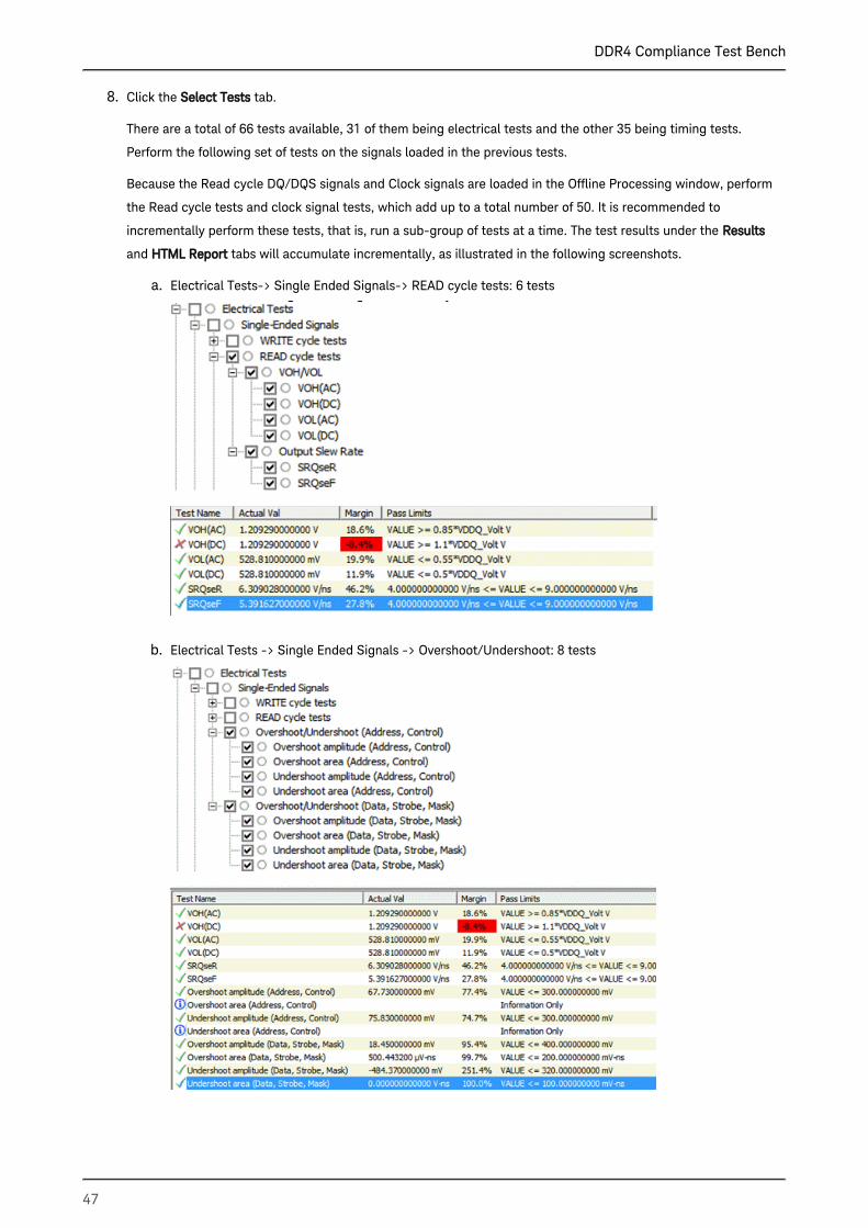
Click the tab.Select Tests
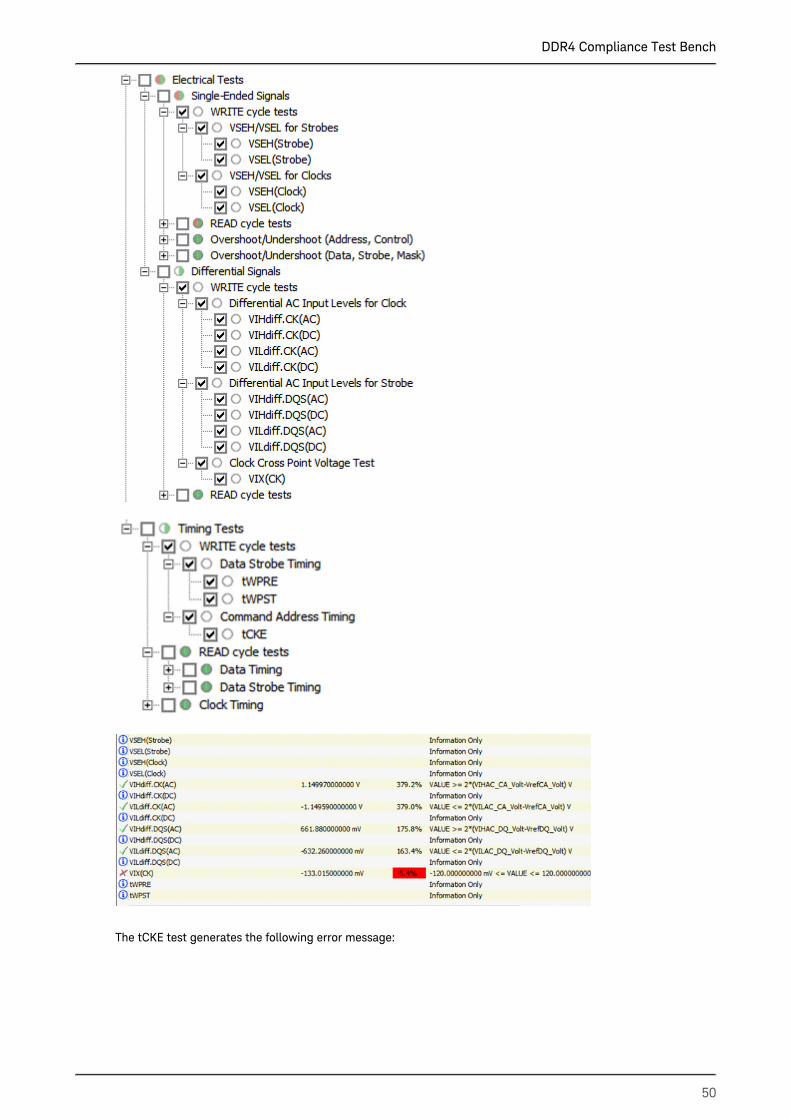
There are a total of 66 tests available, 31 of them being electrical tests and the other 35 being timing tests.
Perform the following set of tests on the signals loaded in the previous tests.
Because the Read cycle DQ/DQS signals and Clock signals are loaded in the Offline Processing window, perform
the Read cycle tests and clock signal tests, which add up to a total number of 50. It is recommended to
incrementally perform these tests, that is, run a sub-group of tests at a time. The test results under the Results
and tabs will accumulate incrementally, as illustrated in the following screenshots.HTML Report
Electrical Tests-> Single Ended Signals-> READ cycle tests: 6 tests
Electrical Tests -> Single Ended Signals -> Overshoot/Undershoot: 8 tests
DDR4 Compliance Test Bench
48
8.
c.
d.
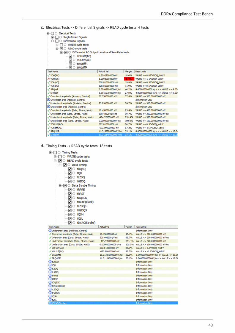
Electrical Tests -> Differential Signals -> READ cycle tests: 4 tests
Timing Tests -> READ cycle tests: 13 tests
DDR4 Compliance Test Bench
49
8.
e.
9.
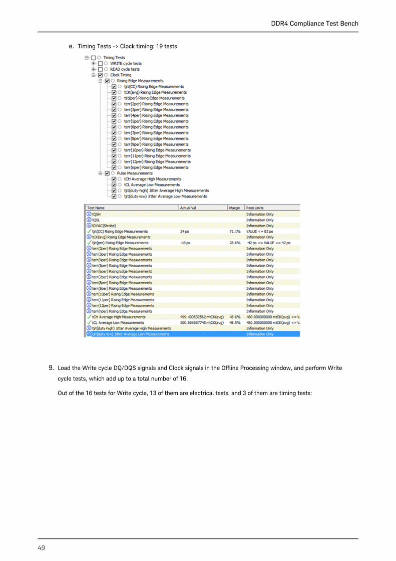
Timing Tests -> Clock timing: 19 tests
Load the Write cycle DQ/DQS signals and Clock signals in the Offline Processing window, and perform Write
cycle tests, which add up to a total number of 16.
Out of the 16 tests for Write cycle, 13 of them are electrical tests, and 3 of them are timing tests:
DDR4 Compliance Test Bench
50
9.
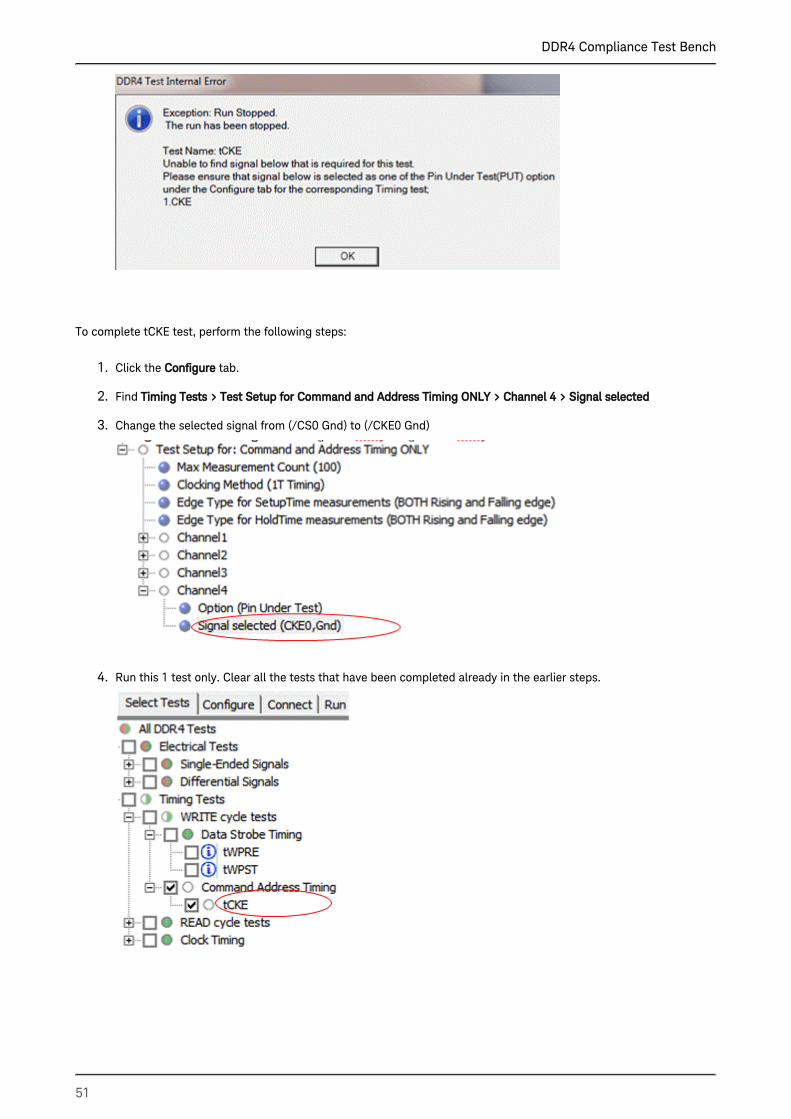
The tCKE test generates the following error message:
DDR4 Compliance Test Bench
51
9.
1.
2.
3.
4.
To complete tCKE test, perform the following steps:
Click the tab.Configure
Find Timing Tests > Test Setup for Command and Address Timing ONLY > Channel 4 > Signal selected
Change the selected signal from (/CS0 Gnd) to (/CKE0 Gnd)
Run this 1 test only. Clear all the tests that have been completed already in the earlier steps.
DDR4 Compliance Test Bench
52
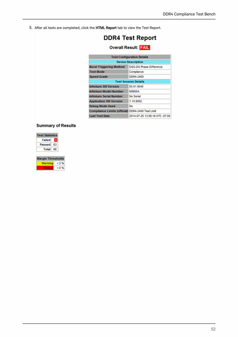
5. After all tests are completed, click the tab to view the Test Report.HTML Report
DDR4 Compliance Test Bench
53
1.
2.
Troubleshooting Invalid WRITE Bursts Error in DDR4
Troubleshooting Invalid Write Bursts Error in DDR4You might get invalid test results for VSEH/VSEL for strobes. The following error message is displayed:
Unable to find valid write bursts
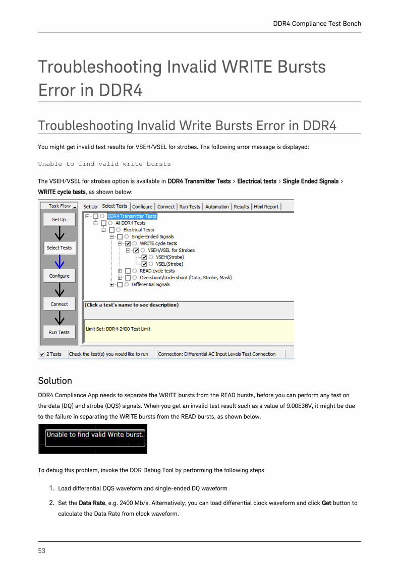
The VSEH/VSEL for strobes option is available in > > > DDR4 Transmitter Tests Electrical tests Single Ended Signals
, as shown below:WRITE cycle tests
SolutionDDR4 Compliance App needs to separate the WRITE bursts from the READ bursts, before you can perform any test on
the data (DQ) and strobe (DQS) signals. When you get an invalid test result such as a value of 9.00E36V, it might be due
to the failure in separating the WRITE bursts from the READ bursts, as shown below.
To debug this problem, invoke the DDR Debug Tool by performing the following steps
Load differential DQS waveform and single-ended DQ waveform
Set the , e.g. 2400 Mb/s. Alternatively, you can load differential clock waveform and click button to Data Rate Get
calculate the Data Rate from clock waveform.
DDR4 Compliance Test Bench
54
3.
4.
5.
Examine the p-p (peak-to-peak) voltage of the DQS waveform. If the p-p voltage is smaller than the default value
of 0.5V for “Burst Envelope Threshold” (BurstEnvThres), change the threshold to make sure it is lower than the
actual DQS p-p voltage.
Examine the p-p (peak-to-peak) voltage of the DQ waveform. If the p-p voltage is smaller than the default value
of 0.5V for “Data Voltage Range” (DataVoltRange), change the DataVoltRange to make sure it is lower than the
actual DQ p-p voltage.
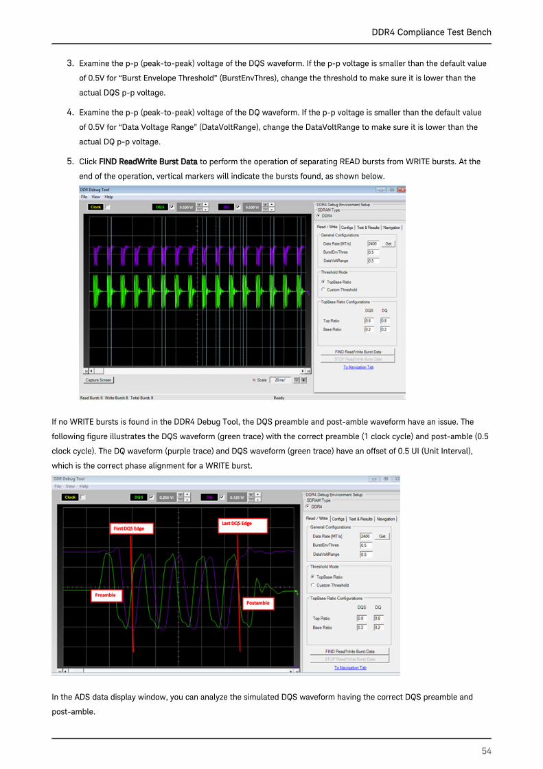
Click to perform the operation of separating READ bursts from WRITE bursts. At the FIND ReadWrite Burst Data
end of the operation, vertical markers will indicate the bursts found, as shown below.
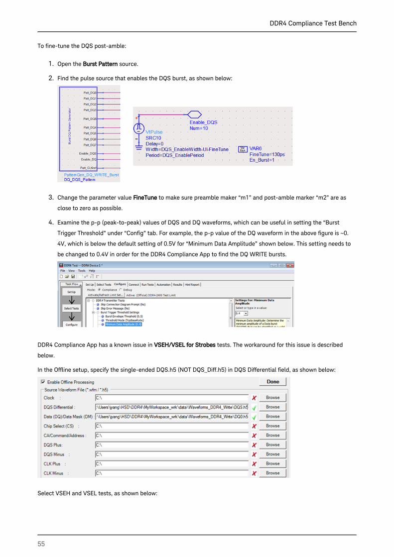
If no WRITE bursts is found in the DDR4 Debug Tool, the DQS preamble and post-amble waveform have an issue. The
following figure illustrates the DQS waveform (green trace) with the correct preamble (1 clock cycle) and post-amble (0.5
clock cycle). The DQ waveform (purple trace) and DQS waveform (green trace) have an offset of 0.5 UI (Unit Interval),
which is the correct phase alignment for a WRITE burst.
In the ADS data display window, you can analyze the simulated DQS waveform having the correct DQS preamble and
post-amble.
DDR4 Compliance Test Bench
55
1.
2.
3.
4.
To fine-tune the DQS post-amble:
Open the source.Burst Pattern
Find the pulse source that enables the DQS burst, as shown below:
Change the parameter value to make sure preamble maker “m1” and post-amble marker “m2” are as FineTune
close to zero as possible.
Examine the p-p (peak-to-peak) values of DQS and DQ waveforms, which can be useful in setting the “Burst
Trigger Threshold” under “Config” tab. For example, the p-p value of the DQ waveform in the above figure is ~0.
4V, which is below the default setting of 0.5V for “Minimum Data Amplitude” shown below. This setting needs to
be changed to 0.4V in order for the DDR4 Compliance App to find the DQ WRITE bursts.
DDR4 Compliance App has a known issue in tests. The workaround for this issue is described VSEH/VSEL for Strobes
below.
In the Offline setup, specify the single-ended DQS.h5 (NOT DQS_Diff.h5) in DQS Differential field, as shown below:
Select VSEH and VSEL tests, as shown below:
DDR4 Compliance Test Bench
56
Run the tests and get the following results: