DATE 2003 Master Course: Design and Design Methods for RF ...rutenbar/pdf/rutenbar-date03tut.pdf ·...
24
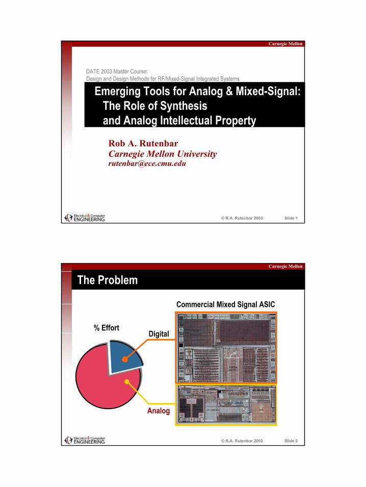
R.A. Rutenbar, 2001 © R.A. Rutenbar 2003 Slide 1 Carnegie Mellon Rob A. Rutenbar Carnegie Mellon University [email protected] Emerging Tools for Analog & Mixed-Signal: The Role of Synthesis and Analog Intellectual Property DATE 2003 Master Course: Design and Design Methods for RF/Mixed-Signal Integrated Systems © R.A. Rutenbar 2003 Slide 2 Carnegie Mellon The Problem Commercial Mixed Signal ASIC Analog Digital % Effort
Transcript of DATE 2003 Master Course: Design and Design Methods for RF ...rutenbar/pdf/rutenbar-date03tut.pdf ·...
HOTCHIPS 2001
©R.A. Rutenbar, 2001 1
© R.A. Rutenbar 2003 Slide 1
Carnegie Mellon
Rob A. RutenbarCarnegie Mellon [email protected]
Emerging Tools for Analog & Mixed-Signal:The Role of Synthesis and Analog Intellectual Property
DATE 2003 Master Course: Design and Design Methods for RF/Mixed-Signal Integrated Systems
© R.A. Rutenbar 2003 Slide 2
Carnegie Mellon
The Problem
Commercial Mixed Signal ASIC
Analog
Digital% Effort

HOTCHIPS 2001
©R.A. Rutenbar, 2001 2
© R.A. Rutenbar 2003 Slide 3
Carnegie Mellon
The Reason for the Problem
Digital MethodologyCAD toolsAbstractionReuse & IPAnalog Methodology
CAD toolsAbstractionReuse & IP
© R.A. Rutenbar 2003 Slide 4
Carnegie Mellon
Scaling for Analog: Why It Doesn’t Help…Cost/Area
Generation
SiGeSOI
CMOS
Area/Ckt
Generation
Analog Ckt Area
DigitalCkt Area
Cost/Ckt
Generation
Analog $$/Ckt
Digital $$/Ckt
D
ADA
DA
Yesterday’sCMOS
Today’sCMOS
Tomorrow’sCMOS
[From David Harame, IBM MD Design Forum, March 2002]

HOTCHIPS 2001
©R.A. Rutenbar, 2001 3
© R.A. Rutenbar 2003 Slide 5
Carnegie Mellon
Today’s Talk: Emerging Solutions
EDA strategies for analog blocks
Core technology: analog synthesis
Ideal end goal: analog intellectual property (IP)
Industrial examples: how far along are we…?
© R.A. Rutenbar 2003 Slide 6
Carnegie Mellon
Where Do We Start: One Analog CellMixed-Signal System-on-Chip
Analog
Digital
Vref CellExample:one analog cell on
analog-side of amixed-signal ASIC

HOTCHIPS 2001
©R.A. Rutenbar, 2001 4
© R.A. Rutenbar 2003 Slide 7
Carnegie Mellon
Gain 60dBUGF 111MHzPhase 60degSlew 2V/usCMRR: 60dBPSRR: 70dBTHD: 1%...
11/4 11/4
42/3 42/3
3/3 3/3
3/4 3/4
160/12
10pF
¿ 10pF
In- In+ 23µA54µA 3/52
Specification Circuit topology & sizing Physical layout
Just What Is An “Analog Cell?”
Typical analog cell~5-150 devices (if bigger, usually use some hierarchy)Active devices (FET, BJT, etc) and passives (R, L, C)Often requires precision devices/passives for performanceOften requires sensitive device placement, wiring
Need all 3 of these to have a “complete” cell
© R.A. Rutenbar 2003 Slide 8
Carnegie Mellon
Role of Digital Cells in Digital System Design
Digital ASIC design Often starts from assumed library of cells (maybe some cores too)Supports changes in cell-library; assumed part of methodologyCell libraries heavily reused across different designs
DigitalHDL
LogicSynthesis
TechMapping
PhysicalDesign
Gate-Level Cell Library

HOTCHIPS 2001
©R.A. Rutenbar, 2001 5
© R.A. Rutenbar 2003 Slide 9
Carnegie Mellon
Where Do Digital Cells Come From?
Foundries:Optimized for
this fab
3rd Party IP:Emphasize
portability, quick use
Migration Tools:Old cells -> new cells
Migrate
Manual, Custom Design:Proprietary or custom library
© R.A. Rutenbar 2003 Slide 10
Carnegie Mellon
Where Do Analog Cells Come From?
From analog designersMainly manual design Often, manual redesignAlmost no reuse
Why is this?
—+
HOTCHIPS 2001
©R.A. Rutenbar, 2001 6
© R.A. Rutenbar 2003 Slide 11
Carnegie Mellon
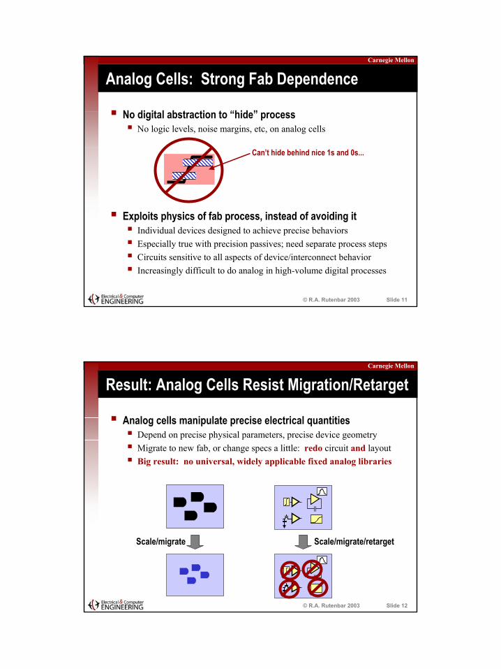
No digital abstraction to “hide” processNo logic levels, noise margins, etc, on analog cells
Exploits physics of fab process, instead of avoiding itIndividual devices designed to achieve precise behaviorsEspecially true with precision passives; need separate process stepsCircuits sensitive to all aspects of device/interconnect behaviorIncreasingly difficult to do analog in high-volume digital processes
Analog Cells: Strong Fab Dependence
Can’t hide behind nice 1s and 0s...
© R.A. Rutenbar 2003 Slide 12
Carnegie Mellon
Result: Analog Cells Resist Migration/Retarget
Analog cells manipulate precise electrical quantitiesDepend on precise physical parameters, precise device geometryMigrate to new fab, or change specs a little: redo circuit and layoutBig result: no universal, widely applicable fixed analog libraries
Scale/migrate Scale/migrate/retarget

HOTCHIPS 2001
©R.A. Rutenbar, 2001 7
© R.A. Rutenbar 2003 Slide 13
Carnegie Mellon
Analog Cell Libraries: Dimensionality
Problem: many continuous specs for analog cells
Can’t just build a practical-size, universal analog library
−+ =
11/4 11/4
42/3 42/3
3/3 3/3
3/4 3/4
160/12
10pF
¿ 10pF
In- In+ 23µA54µA 3/52
10 independentperformancespecifications
=
Spec=LOWSpec=HIGH
variantsfor ALL
combinations
X = ~ 1000 variantsfor just this cell
© R.A. Rutenbar 2003 Slide 14
Carnegie Mellon
OK—What Do We Really Want Here…?
How do people put big digital ASICs together today?In big pieces, compiling & synthesizing the IP block as needed
Digital ASICI need an Embedded SRAM:Use a RAM generator tool
I need a Regular Datapath:Use a Datapath compiler
I need a Register File: Use a RegFile compiler
I need 500,000 gates of random logic:
Use logic synthesis followed by
physical synthesis

HOTCHIPS 2001
©R.A. Rutenbar, 2001 8
© R.A. Rutenbar 2003 Slide 15
Carnegie Mellon
On the Analog Side of a Mixed-Signal SoC…
We want the same sort of functionalitySynthesis: for the custom cells/blocks that determine analog performanceGenerators: for the less custom, more regular stuff left over
Mixed-SignalASIC
I need a custom Video Amplifier
Use analog circuit & physical synthesis
I need a custom Voltage Reference
Use analog circuit & physical synthesis
I need a set of custom High-Precision PassivesUse a Device generator
I need a custom A/D Converter Use a mix of generators and
custom analog synthesis
© R.A. Rutenbar 2003 Slide 16
Carnegie Mellon
Analog IP
Device-level IPGenerators for individual devices & small precision groups
Cell-level IPSynthesizable buildingblocks, from a libraryof useful topologies
System-level IPSynthesizable blocksfor useful chip-levelfunctions

HOTCHIPS 2001
©R.A. Rutenbar, 2001 9
© R.A. Rutenbar 2003 Slide 17
Carnegie Mellon
Analog Device-Level IP
Basic ideaAnalog cells require “difficult” device structuresMay need large devices, aggressive matching, unusual precisionCan save layouts in library, or better: write layout generatorsMay be provided by your foundry, or tool supplier
Most common example: Cadence PCELL technology
Device IP Gen.
Ν7
Digital FET(for contrast)
Analog FET
© R.A. Rutenbar 2003 Slide 18
Carnegie Mellon
Large Can Mean Very Large, Too
1 FET A fewcapacitors
A smallCPU core
digital
analog

HOTCHIPS 2001
©R.A. Rutenbar, 2001 10
© R.A. Rutenbar 2003 Slide 19
Carnegie Mellon
Industrial Ex: Precision Interdig Resistor ArrayA single highly precise passive analog component can be very complex, very large, difficult to design—need automation
Courtesy Neolinear
© R.A. Rutenbar 2003 Slide 20
Carnegie Mellon
Foundation of Analog IP: Analog Synthesis
Today’s emerging industrial analog synthesis flow
Cell topology+ specs
CircuitEvaluation
Engine(simulator)
CircuitSynthesis
Engine(num. search)
LayoutEvaluation
Engine(3D extractor)
PhysicalSynthesis
Engine(geom. search)
Interconnectmodeling
Cell specs
BehavioralModels
BehavioralModels
∑i xijsiyj
rj
W=…L=…
Behavioral model
Sizedschematic
Physicallayout
Interconnectmodel
Inte
rcon
nect
beh
avio
r

HOTCHIPS 2001
©R.A. Rutenbar, 2001 11
© R.A. Rutenbar 2003 Slide 21
Carnegie Mellon
Cell-Level Synthesis: Framework
Most approaches have this overall structure
Uses heuristic or numerical searchOptimization engine: proposes candidate circuit solutionsEvaluation engine: evaluates quality of each candidateCost-based search: cost metric represents “goodness” of design
EvaluatedCircuit
Performance
Candidate CircuitDesign
OptimizationEngine
EvaluationEngine
© R.A. Rutenbar 2003 Slide 22
Carnegie Mellon
20 Years of Synthesis Distilled Onto 1 Slide…
Optimization EngineNumericaloptimizer
(3) Symbolic analysis
Evaluation EngineAuto-derived eqns
I = K’/2 W/L (Vgs-Vt)2
Optimization EngineGlobaloptimizer
(4) Simulation-Based
Evaluation EngineIndustrial simulator
Optimization Engine
You
(1) Scripting
Evaluation EngineEqns you write: I = K’/2 W/L (Vgs-Vt)2
Evaluation EngineEqns you write: I = K’/2 W/L (Vgs-Vt)2
Optimization Engine
(2) Equation-Based
Numericaloptimizer

HOTCHIPS 2001
©R.A. Rutenbar, 2001 12
© R.A. Rutenbar 2003 Slide 23
Carnegie Mellon
Only One of these Widely Successful…
Optimization EngineGlobaloptimizer
(4) Simulation-Based
Evaluation EngineIndustrial simulator
Optimization EngineNumericaloptimizer
(3) Symbolic analysis
Evaluation EngineAuto-derived eqns
I = K’/2 W/L (Vgs-Vt)2
Optimization EngineNumericaloptimizer
(3) Symbolic analysis
Evaluation EngineAuto-derived eqns
I = K’/2 W/L (Vgs-Vt)2
Optimization Engine
You
(1) Scripting
Evaluation EngineEqns you write: I = K’/2 W/L (Vgs-Vt)2
Evaluation EngineEqns you write: I = K’/2 W/L (Vgs-Vt)2
Optimization Engine
(2) Equation-Based
Numericaloptimizer
© R.A. Rutenbar 2003 Slide 24
Carnegie Mellon
Large CMU Sim-Based Example: TI ADSL CODEC
[R. Hester, et al.. IEEE Int’l Solid-State Circuits Conf., 1999][R. Phelps, et al., ACM/IEEE Design Automation Conf, 2000]
EQFEqualizer
1.54MHz, corner
0dB gain
AnalogLow-Pass
Filter
0-25dB/MHzgain, in
5dB/MHzsteps
ProgrammableGain
Amplifier
2.5-11.5 dBgain, in0.25dBsteps
Analog toDigital
Converter
4416KHz14bits
DigitalLow-Pass
Filter
1.1MHzcorner,
0dB gain
Decimation
Input fc 4416KHzOutput fc2208KHz

HOTCHIPS 2001
©R.A. Rutenbar, 2001 13
© R.A. Rutenbar 2003 Slide 25
Carnegie Mellon
EQF: What It Does
EQF = equalizer + 4th-order elliptical low-pass C-T filterProgrammably amplifies signal (since attenuated by copper)Filters data from spectrum (avoiding phone voice band)
Spectral Mask
0
-20
-40
-60
-800 2 4 6 8 10 12 14 16
Freq (MHz)
Gai
n (d
B)
Gai
n (d
B)
0
-10
10
20
30
Freq (MHz)0 0.4 0.8 1.2 1.6
All 6 Eq Settings Flat Eq Setting
Eq0Eq1
Eq2Eq3Eq4Eq5
Eq0
© R.A. Rutenbar 2003 Slide 26
Carnegie Mellon
EQF Block: What It Looks Like5 low-noise amps, ~100 passives, 36 program switches, 6 op-modes, ~400 devices, flat; ~2-3hrs to SPICE
-+
-+
-+
-+
-+
AA
BB
Vin Vout-+
-+
-+
-+
-+
AA
BB
Vin Vout
A B
OM
OM
OP

HOTCHIPS 2001
©R.A. Rutenbar, 2001 14
© R.A. Rutenbar 2003 Slide 27
Carnegie Mellon
Synthesis Results: Spectral Mask
~ 2 months designed manuallySynthesized automatically overnight 0 2 4 6 8 10 12 14 16
Freq (MHz)
Eq0 Spectral Mask
0
-20
-40
-60
-80G
ain
(dB
)
Eq0 Passband
Freq (MHz)0 0.4 0.8 1.2 1.6
0
-2
Gai
n (d
B)
-4-6
-8
CMU1
CMU2
CMU3
TI Hand
© R.A. Rutenbar 2003 Slide 28
Carnegie Mellon
Industrial Applications of Synthesis IdeasInfineon result [Hennig, Sommer, Charlack, DATE02]
NeoCircuit(Sizing)
Neolinear® synthesis
Performance Specification Result Supply voltage 3.3 V Load 10 MΩ || 10 pF DC Gain > 90 dB 90.47 dB Gain margin > 3 3.152 Phase margin > 60° 60.49° Unity-gain frequency > 2 MHz 2.972 MHz PSRR > 100 dB 120.9 dB CMRR > 110 dB 117.7 dB Offset < 1 mV 752.5 µV Slew rate > 1 V/µs, maximize! 2.331 V/µs Settling time < 500 ns 490.9 ns Overshoot < 50 mV 5.673 mV Power < 300 µW, minimize! 297.4 µW
initial manual
NeoCircuit
CMOS Folded Cascode Amp

HOTCHIPS 2001
©R.A. Rutenbar, 2001 15
© R.A. Rutenbar 2003 Slide 29
Carnegie Mellon
RF Too: 2.1GHz LNA in IBM 0.5um SiGeCMU result
[Zhang, Dengi, Carley, RFIC Symp02]
LE
Q1(6)
Q2 Cout
LloadIbias
Lin
Q3 (1)
LE
Q1(6)
Q2 Cout
LloadIbias
Lin
Q3 (1)
-20dB<-15dBGmin
-39dB<-30dBS124>1K_factor
-21dB<-20dBS22
3.7mAMin. <5mAICC
-15dB<-15dBS11-15dBm>-20dBmInput_P1dB-6dBm>-10dBmInput-Ip31.2dB<1.5dBNF16dB>15dBS21ResultsSpecificationsPerformance
GoptNFNFmin
-16 –15 -14 -13 -12 -11 -10
Gopt (dB) NF/NFmin (dB)-15
-20
-25
-30
-35
-40
1.35
1.3
1.25
1.2
1.15
1.1
Selected design point
S11 (dB)
© R.A. Rutenbar 2003 Slide 30
Carnegie Mellon
Cell-Level Analog Layout Synthesis
Basic task
Major strategiesAnalog-specific placement (eg, wells, guard rings, symmetries)Analog-specific routing (symmetries, balance, crosstalk)Analog-specific compaction (respecting these electrical constraints)
11/4 11/4
42/3 42/3
3/3 3/3
3/4 3/4
160/12
10pF
¿ 10pF
In- In+ 23µA54µA 3/52 Layout
Synthesis
From schematic +geometric constraintsto physical layout

HOTCHIPS 2001
©R.A. Rutenbar, 2001 16
© R.A. Rutenbar 2003 Slide 31
Carnegie Mellon
Analog Physical Layout Example: Close-up
This exampleCMOS~50 devicesLayout < 1 hr
Courtesy Neolinear
© R.A. Rutenbar 2003 Slide 32
Carnegie Mellon
Big Idea: Analog IP = Capture + Synthesis
Commercial example from Neolinear NeoCircuit/NeoCell flowUnsized commercial
diff-amp cell
PhysicalSynthesis
0.6um proprietary CMOS fab
CircuitSynthesis W=83
L=6

HOTCHIPS 2001
©R.A. Rutenbar, 2001 17
© R.A. Rutenbar 2003 Slide 33
Carnegie Mellon
Big Idea: Analog IP = Capture + Synthesis
Commercial example from Neolinear NeoCircuit/NeoCell flowUnsized commercial
diff-amp cell
PhysicalSynthesis
CircuitSynthesis
PhysicalSynthesis
0.6um proprietary CMOS fab
TSMC 0.35um CMOS fab
78% less area; 42% less power
CircuitSynthesis W=83
L=6
© R.A. Rutenbar 2003 Slide 34
Carnegie Mellon
Industrial Front-to-Back Synthesis Example
STMicroelectronics result [Shah, Dugalleix, Lemery DATE02]
BIASING AMPLIFIER
NeoCircuit(sizing)
NeoCell(layout)0.18µm
0.12µm NeoCircuit(sizing)
NeoCell(layout)
Area: 0.004 mm2
Power: 1.1 mW
Area: 0.009 mm2
Power: 9.15 mW
Neolinear analog flow
9.15 mW
1900 V/µs
7.4 ns
48o
1.1 GHz
70 dB
RESULTS0.18µm Corners
1.1 mW< 10 mWPower
1620 V/µs> 400 V/µsSlew
5.77 ns< 8 nsSettling Time
49.2o> 45oPhase Margin
2.17 GHz> 600 MHzUGF
70.3 dB> 70 dBDC Gain
RESULTS0.12µm Corners
GOALSat 0.18µm
9.15 mW
1900 V/µs
7.4 ns
48o
1.1 GHz
70 dB
RESULTS0.18µm Corners
1.1 mW< 10 mWPower
1620 V/µs> 400 V/µsSlew
5.77 ns< 8 nsSettling Time
49.2o> 45oPhase Margin
2.17 GHz> 600 MHzUGF
70.3 dB> 70 dBDC Gain
RESULTS0.12µm Corners
GOALSat 0.18µm

HOTCHIPS 2001
©R.A. Rutenbar, 2001 18
© R.A. Rutenbar 2003 Slide 35
Carnegie Mellon
Measuring Productivity Gains
STMicroelectronics: ~10x design cycle reduction [Shah, Dugalleix, Lemery DATE02]
0
5
10
15
20
25
30
35
0.18umManual
0.18umNeolinear
0.12umManual
0.12umNelinear
LayoutSizing
BIASING AMPLIFIER
Design Time (Days)
0.18µm 0.12µm
© R.A. Rutenbar 2003 Slide 36
Carnegie Mellon
New Flow Possibilities: Incremental Redesign
Synthesis:Sizing/Bias
Synthesis:Layout Extraction
IncrementalRe-Synthesis:
Sizing/Bias
IncrementalRe-Synthesis:
Layout
Shared Design Constraints
Oops—missed specs due to parasitics.
Incrementallyresynthesize sizing & layout to repair this.

HOTCHIPS 2001
©R.A. Rutenbar, 2001 19
© R.A. Rutenbar 2003 Slide 37
Carnegie Mellon
Incremental Redesign: Auto Small Changes
100M 1G 10G
101
100
10-1
~500MHz
First sizing run,no layout parasitics
With parasiticsfrom initial layout
Incrementalredesign
1st design Incrementalredesign
Gain
© R.A. Rutenbar 2003 Slide 38
Carnegie Mellon
Historically—Why Has All This Been So Hard?
With new synthesis/analysis tools, improved methodologies, & improved attitudes about design—stage set for radical changes
Too much art,not enough science
Mediocreanalog point tools
Aaargh…!Tools!
Ad hoc, incompletecapture of design intent…what theheck is that?

HOTCHIPS 2001
©R.A. Rutenbar, 2001 20
© R.A. Rutenbar 2003 Slide 39
Carnegie Mellon
So—Where Are We?
Emerging commercial synthesis flowFrom topology to GDSII, ~10X fasterMethodology in-place to harvest and archive critical constraints
Analog IP at system levelPLLs, converters, RF systems, etc., are all now being redesigned using synthesis tools “at the bottom”Open questions: how best to represent and sequence these designsteps, now that it’s not all by hand, all the time?
Look at a couple of ongoing examples
© R.A. Rutenbar 2003 Slide 40
Carnegie Mellon
One Example: Neolinear IP Flow
Expert analog designers explore new circuits
Capture constraints Create reusable analog IP“Soft” IP--synthesizable
Other designers design faster/better thru IP reuse
Retarget or migrate fastLearn by “seeing” what’s important from expert IP
NeoCircuitNeoCircuit
NeoCellNeoCell
Analog IP

HOTCHIPS 2001
©R.A. Rutenbar, 2001 21
© R.A. Rutenbar 2003 Slide 41
Carnegie Mellon
NeoIP Library: Soft, Synthesizable Analog LibSample & hold Opamp (CMFB) Gain Stage
Bandgap VRefComparator
Opamp (2stage)
VCO (Diff. Ring)
Diff. Opamp
Bandgap IRef Freq Detector
Charge Pump Divider D FF
© R.A. Rutenbar 2003 Slide 42
Carnegie Mellon
Authored with Cadence
DSP Core
PLL Clock
Authored with Neolinear and Cadence
Results Converter ( FFT )
Authored with Cadence
RAM ( 128 x 16 ) Glue Logic
RAM ( 256 x 16 )
I/O pads
ROM ( 512 x 16A )
Authored with Artisan ROM CompilerAuthored with
Artisan RAM Compiler
Courtesy Artisan, Cadence & Neolinear
Example: Dual-Tone Multi-Frequency DecoderAnalog

HOTCHIPS 2001
©R.A. Rutenbar, 2001 22
© R.A. Rutenbar 2003 Slide 43
Carnegie Mellon
Top block & support logicassembled using Cadence
Authored with Cadence
Authored with NeoCell
Authored with NeoCell
Authored with CadenceAuthored with Cadence
Counter (3-bit)
Voltage-ControlledOscillator
Charge Pump
Divider ( 2-bit )
Phase Detector
Buffers
Bias Xtors
Cadence ® Generic PDK.18 6LM Generic Process
Decoder PLLPushing Inside the PLLAll analog done via custom synthesis on this design
Courtesy Cadence and Neolinear
© R.A. Rutenbar 2003 Slide 44
Carnegie Mellon
DACCMP/BIAS
Digital
Level Shifter
Circuit Results: Toshiba
Porting a data converter from 0.18µm to 0.14µm
DACCMP/BIAS
Digital
Level Shifter
DAC
7X DAC performance improvement, from 10bits @ 7µs to 10bits @ 1µs
Courtesy Neolinear

HOTCHIPS 2001
©R.A. Rutenbar, 2001 23
© R.A. Rutenbar 2003 Slide 45
Carnegie Mellon
DACCMP/BIAS
Digital
Level Shifter
Productivity Results: Toshiba
Porting a data converter from 0.18µm to 0.14µm
DACCMP/BIAS
Digital
Level Shifter
CMP/BIAS
~10X less design timefor this difficult cell
0
10
20
30
40
50
0.18umManual
0.14umNeolinear
Design Time (Days)LayoutSizing
Courtesy Neolinear
© R.A. Rutenbar 2003 Slide 46
Carnegie Mellon
Conclusions
Analog circuits: not getting any easier with scalingIn an SoC world, analog is taking an increasing fraction of the dieThe world is analog; more ASICs will be mixed-signal in future
Mixed-signal design realitiesAnalog cells are not like digital cellsNot as easily library-able; don’t scale; don’t migrateTightly bound to fab process, difficult precision requirements
Design strategiesLess art, more science: better methodologies, real synthesis toolsAnalog IP: design for migrating, retargeting is the next big thingSynthesis technologies are the cornerstone of all analog IP efforts

HOTCHIPS 2001
©R.A. Rutenbar, 2001 24
© R.A. Rutenbar 2003 Slide 47
Carnegie Mellon
To Learn More: Mixed-Signal CAD
Computer-Aided Design of Analog Integrated Circuits and Systems
Rob A. Rutenbar, Georges G. E. Gielen, Brian A. Antao, EditorsHardcover: 768 pages Publisher: IEEEPublished: April 2002ISBN: 047122782X