Datasheet - STR485 - 3.3 V RS485 compatible with 1.8 V I ... · limits have been tested up ±4 kV...
24
DFN10 3 x 3 Features • Half-duplex RS485 transceiver • 1.65 V to 3.6 V supply for data and enable signals • 3 V to 3.6 V supply for bus supply • High speed: up to 20 Mbps data rate • Low speed selected by SLR pin : 250 kbps • Up to 256 transceivers on the bus • Fail safe receiver (bus open, idle and shorted) • Thermal shutdown protection • Low quiescent current in shutdown mode • Extended temperature range : -40 °C to +105 °C • Available in industry standard DFN10 • Bus-pin protection more than: – ±4 kV HBM protection – ±8 kV IEC61000-4-2 contact discharge – ±16 kV IEC61000-4-2 air discharge – Compliant IEC61000-4-4 fast transient burst Class B Description The STR485 is a low power differential line transceiver for data transmission standard RS485 applications in half-duplex mode. Data and enable signals are compatible with 1.8 V or 3.3 V supplies. Two speeds are selectable through SLR pin: fast data rate up to 20 Mbps or slow data rate for extended cable running to 250 kbps. Excessive power dissipation caused by bus contention or faults is prevented by thermal shutdown circuit that forces the driver outputs into a high impedance state. The receiver has a fail-safe feature, which guarantees a high output state when the inputs are left open, shorted or idle. Product status link STR485 3.3 V RS485 compatible with 1.8 V I/Os and selectable speed 20 Mbps or 250 kbps STR485 Datasheet DS12713 - Rev 2 - October 2018 For further information contact your local STMicroelectronics sales office. www.st.com
Transcript of Datasheet - STR485 - 3.3 V RS485 compatible with 1.8 V I ... · limits have been tested up ±4 kV...
DFN10 3 x 3
Features
• Half-duplex RS485 transceiver• 1.65 V to 3.6 V supply for data and enable signals• 3 V to 3.6 V supply for bus supply• High speed: up to 20 Mbps data rate• Low speed selected by SLR pin : 250 kbps• Up to 256 transceivers on the bus• Fail safe receiver (bus open, idle and shorted)• Thermal shutdown protection• Low quiescent current in shutdown mode• Extended temperature range : -40 °C to +105 °C• Available in industry standard DFN10• Bus-pin protection more than:
– ±4 kV HBM protection– ±8 kV IEC61000-4-2 contact discharge– ±16 kV IEC61000-4-2 air discharge– Compliant IEC61000-4-4 fast transient burst Class B
DescriptionThe STR485 is a low power differential line transceiver for data transmissionstandard RS485 applications in half-duplex mode. Data and enable signals arecompatible with 1.8 V or 3.3 V supplies.
Two speeds are selectable through SLR pin: fast data rate up to 20 Mbps or slowdata rate for extended cable running to 250 kbps.
Excessive power dissipation caused by bus contention or faults is prevented bythermal shutdown circuit that forces the driver outputs into a high impedance state.The receiver has a fail-safe feature, which guarantees a high output state when theinputs are left open, shorted or idle.
Product status link
STR485
3.3 V RS485 compatible with 1.8 V I/Os and selectable speed 20 Mbps or 250 kbps
STR485
Datasheet
DS12713 - Rev 2 - October 2018For further information contact your local STMicroelectronics sales office.
www.st.com

1 Pin connections
Figure 1. Pin connections
SLR
GND
VL
R
DE
RE
D
VCC
B
A
Table 1. Pin description
Name Pin I/O Description
VL 1 Logic supply 1.65 V to 3.6 V supply for logic I/O signals
R 2 Digital output Receiver data output
DE 3 Digital input Driver enable input
nRE 4 Digital input Receiver enable input
D 5 Digital input Transmission data input
GND 6 Ground
SLR 7 Digital inputSlew rate select: low = 20 Mbps, high = 250 kbps.
Default to 20 Mbps if SLR is left floating
A 8 Bus I/O Digital bus I/O, A
B 9 Bus I/O Digital bus I/O, B
VCC 10 Bus supply 3 V to 3.6 V supply for A and B bus lines
Figure 2. Typical application schematic
BB
A A
GND GND
VCC
D D
DE DE
R R
RERE
VL SLR
RT120 Ω
RT120 Ω
3.3 V1.8 V
VCC
3.3 V
VLSLR
1.8 V
STR485Pin connections
DS12713 - Rev 2 page 2/24

Figure 3. Example of implementation in a PCB
Adding an ESDA14V2BP6 or ETP01-2821 ST Microelectronics protection device can help the product to sustainan EFT perturbation level up to 4 kV.
STR485Pin connections
DS12713 - Rev 2 page 3/24

2 Truth tables
The STR485 is a half-duplex differential driver/receiver compliant to the RS485 communication standard (ISO-IEC8482). This product is perfectly adapted for low voltage application running with a low power supplies VL,generally set to 1.8 V and VCC set to 3.3 V.These voltages confer a low power consumption to the product.SLR is the data rate selection, this pin could be let floating but it is not recommended; in that case the high speedrate is automatically selected.The SLR pin must be connected to the ground to provide a high speed communication up to 20 Mbps.When this pin is connected to VL power supply, the data rate is limited to 250 kbps more adapted for very longdistance data transmission.
Figure 4. Block diagram
The product is perfectly adapted to run with 256 devices on the same bus thanks to the internal output resistancethat is over 96 kΩ up to 105 °C; this resistance follows the RS485 condition that requests a minimum of 12 kΩ for32 unit loads (UL).The STR485 has internal protection against ESD that protect each device driver output and receiver input. Thelimits have been tested up ±4 kV electrostatic discharge (HBM) and ± 8 kV contact discharge and ± 16 kV airdischarge shocks without latch-up.Another external protections can be used to increase the communication robustness against different perturbationthat can be seen on the application.The power supplies must be well-decoupled by a minimal capacitor of 0.1 µF as closed as possible to the devicepower supply input. Moreover, the capacitor should be higher on the application with a minimum of 1 µF aroundthe device.The device operating range is set from VL = 1.65 V to 3.6 V and for Vcc = 3.0 V to 3.6 V. In any case VCC mustbe higher or equal than VL.The applications should respect this voltage constraints to let the application communication device run to thebest conditions.
STR485Truth tables
DS12713 - Rev 2 page 4/24
Figure 5. Example of typical application
B B
B B
A
A A
A
GND
GND GND
GND
VCC
VCC VCC
VCC
D
D D
D
DE
DE DE
DE
R
R R
R
RE
RERE
RE
VL
VL
VL
VLSLR
SLR SLR
SLR
RT120Ω
RT120Ω
Table 2. Driver truth table
INPUT D ENABLE DE OUTPUT A OUTPUT B Function
H H H L Actively drive bus high
L H L H Actively drive bus low
X L Z Z Driver disabled
X Open Z Z Driver disabled by default
Open H H L Actively drive bus high by default
Table 3. Receiver truth table
Differential input VID = VA -VB ENABLE RE OUTPUT R Function
VID > VIT+ L H Receive valid bus high
VIT- < VID < VIT+ L ? Indeterminate bus state
VID < VIT- L L Receive valid bus low
X H Z Receiver disabled
X OPEN Z Receiver disabled by default
Open-circuit bus L H Fail safe high output
Short-circuit bus L H Fail safe high output
Idle (terminated) bus L H Fail safe high output
Table 4. Speed selection, SLR pin configuration
SLR Data rate Typical tr / tf
VL 250 kbps 200 ns
GND or OPEN 20 Mbps 7 ns
STR485Truth tables
DS12713 - Rev 2 page 5/24

3 Absolute maximum ratings and operating conditions
Table 5. Absolute maximum ratings
Symbol Parameter Min. Max. Unit
VL Control supply voltage -0.5 4 V
VCC Bus supply voltage -0.5 4.8 V
Voltage range at A or B inputs -13 13 V
Input voltage range at any logic pin -0.3 VL+0.3 V
Receiver output current -12 12 mA
TJ Junction temperature 170 °C
Tstg Storage temperature -65 150 °C
ESD
IEC 61000-4-2 ESD (air-gap discharge), bus terminals and GND ± 16 kV
IEC 61000-4-2 ESD (contact discharge), bus terminals and GN ± 8 kV
IEC 61000-4-4 EFT (fast transient or burst) bus terminals and GND ± 2 kV
JEDEC standard 22, test method A114, HBM, all terminals ± 4 kV
JEDEC standard 22, test method C101, (charged device model), all pins ± 1.5 kV
Note: All voltage values, except the differential voltage, are with respect to network ground terminal.
Table 6. Operating conditions
Symbol Parameter Min. Typ. Max. Unit
VL Control supply voltage 1.65 3.6
V
VCC Bus supply voltage 3 3.3 3.6
VI Input level at any bus terminal (separately or common mode) -7 12
VIHHigh level input voltage (driver, driver enabled, receiver enable inputs, and slew rateselect) 0.7×VL VL
VILLow level input voltage (driver, driver enable, receiver enable inputs, and slew rateselect) 0 0.3×VL
VID Differential input voltage -12 12
IOOutput current / driver -80 80
mAOutput current / receiver - 2 2
RL Differential load resistance 54 60 Ω
CL Differential load capacitance 50 pF
DRSignaling rate / SLR = ‘0’ 20 Mbps
Signaling rate / SLR = ‘1’ 250 kbps
TA Operating free-air temperature -40 105 °C
Operation is specified for internal (junction temperature) up to 150 °C. Self-heating due to internal powerdissipation should be considered for each application. Maximum junction temperature is internally limited by thethermal shut-down circuit which disables the driver outputs when the junction temperature reaches 165 °C.
STR485Absolute maximum ratings and operating conditions
DS12713 - Rev 2 page 6/24

Table 7. Thermal information
Symbol Parameter Min. Typ. Max. Unit
Rth-ja Thermal resistance, junction-to-ambient 40°C/W
Rth-jc Thermal resistance, junction-to-case 5.2
STR485Absolute maximum ratings and operating conditions
DS12713 - Rev 2 page 7/24

4 Electrical characteristics
Table 8. Receiver: over recommended operating conditions (unless otherwise specified. Please, see"Operating conditions" table)
Symbol Parameter Test conditions Min. Typ. Max. Unit
Receiver/DC
VIT+Positive-going receiverdifferential input voltagethreshold
(1) -60 -20
mVVIT-Negative-going receiverdifferential input voltagethreshold
-200 -130 (1)
VHYS
Receiver differential inputvoltage thresholdhysteresis (VIT+ - VIT- )(1)
40 70
VOHReceiver high-leveloutput voltage
VL = 1.65 V, IOH = - 2 mA 1.25 1.45
VVL = 3 V, IOH = - 2 mA 2.75 2.9
VOLReceiver low-level outputvoltage
VL = 1.65 V, IOL = 2 mA 0.2 0.45
VL = 3 V, IOL = 2 mA 0.1 0.25
CODDifferential outputcapacitance 15 pF
IOZReceiver output high-impedance current VO = 0 V or VL, nRE at VL -1 1 µA
RinReceiver inputimpedance
-7 V ≤ Vincm ≤ +12 V
-40 °C ≤ Temp ≤ 105 °C96 (2) kΩ
IIReceiver input current(disabled driver)
1V65 < VL < 3.3 V, VCC = 3.3 V 85(2)
µAVI = 12 V, -40 °C ≤ Temp ≤ 105 ° 125(2)
VI = -7 V, -40 °C ≤ Temp ≤ 105 ° -100(2)
Receiver / switching characteristics, SLR = ‘X’
tr, tfReceiver output rise/falltime
CL=15 pF
5 15
ns
tPHL, tPLHReceiver propagationdelay time 15 25 60
tSK(P)Receiver pulse skew, |tPHL – tPLH| 15
tPLZ, tPHZ Receiver disable time 12 20
tPLZ, tPZH, tPZL,tPZH
Receiver enable time
Driver enabled CL=15 pF with 1 kΩ 15 80
Driver disabled CL=15 pF with1 kΩ 2 8 µs
1. Under any specific conditions, VIT+, is specified to be at least VHYS higher than VIT-
2. Guaranteed by design simulation in temperature.
STR485Electrical characteristics
DS12713 - Rev 2 page 8/24

Table 9. Driver: over recommended operating conditions (unless otherwise specified. Please, see"Operating conditions" table)
Symbol Parameter Test conditions Min. Typ. Max. Unit
DC driver/ DC
IIDriver input, driver enable,and receiver enable inputcurrent
-2 2 µA
|VOD| Driver differential outputvoltage magnitude
RL = 60 Ω, 375 Ω oneach output to –7 V to12
1.5 2
VRL = 54 Ω (RS-485) 1.5 2
RL = 100 Ω (RS-422)TJ ≥ 0 °C, VCC ≥ 3.2 2
Δ|VOD|Change in magnitude ofdriver differential outputvoltage
RL = 54 Ω, CL = 50 pF -50 0 50 mV
V°C(SS)Steady-state common-mode output voltage
Center of two 27-Ωload resistors
1 VCC/2 3 V
ΔV°CChange in differentialdriver output common-mode voltage
-50 0 50
mV
V°C(PP)Peak-to-peak drivercommon-mode outputvoltage
500
Driver/switching characteristics, SLR='1', 250 kps, bit time ≥ 4 µs
tr, tfDriver differential outputrise/fall time
RL=54 Ω, CL=50 pF
0.05 0.2 1
tPHL, tPLHDriver propagation delaytime 0.4 1 1.5
tSK(P)Driver pulse skew, |tPHL –tPLH| 0.3
tPLZ, tPHZ Driver disable time 0.017 0.035
tPLZ, tPZH Driver enable time
Receiver enabledCL=50 pF with 110 kΩ 0.7 1.2
Receiver disabledCL=50 pF with 110 kΩ 1.64 2.4 µs
Driver/switching characteristics, SLR= '0', 20 Mbps, bit time ≥ 50 ns
tr, tfDriver differential outputrise/fall time
RL=54 Ω, CL=50 pF
4 7 15
ns
tPHL, tPLH Driver propagation delay 6 12 25
tSK(P)Driver pulse skew, |tPHL –tPLH| 4
tPLZ, tPHZ Driver disable time 17 40
tPZL, tPZH Driver enable timeReceiver enabled 9 18
Receiver disabled 1 2.4 µs
STR485Electrical characteristics
DS12713 - Rev 2 page 9/24

Table 10. Supply current and protections: over recommended operating conditions (unless otherwisespecified. Please, see "Operating conditions" table)
Symbol Parameter Conditions Min. Typ. Max. Unit
Supply current
ICCSupply current(quiescent)
Driver and receiver enabled
DE = VL, RE = GND, noload, Tamb
625
µADriver and receiver enabled
DE = VL, RE = GND, noload, T<105 °C
900 (1)
Driver enabled, receiverdisabled
DE = VCC, =VL, No load,Tamb
315
Driver enabled, receiverdisabled
DE = VCC, =VL, No load, T <105 °C
550 (1)
Driver disabled, receiverenabled
DE = GND, =GND, No Load515 700
Driver and receiver disabled
DE = GND, =VL, no load
[-40 °C, 105 °C]
0.5 3
TTSDThermal shutdownthreshold 165
°CTTSD_HYS
Thermal shutdownhysteresis 15
IOSDriver short-circuitoutput current -7 V < VSHORT < + 12 V -250 250 mA
1. Guaranteed by simulation.
STR485Electrical characteristics
DS12713 - Rev 2 page 10/24
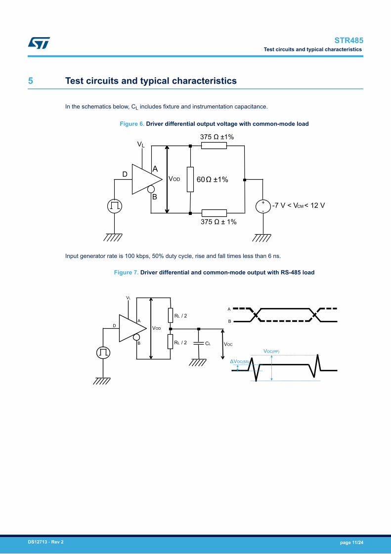
5 Test circuits and typical characteristics
In the schematics below, CL includes fixture and instrumentation capacitance.
Figure 6. Driver differential output voltage with common-mode load
375 Ω ±1%
375 Ω ± 1%
60 Ω ±1%
+-
-7 V < V CM< 12 V
D
VL
A
B
VOD
Input generator rate is 100 kbps, 50% duty cycle, rise and fall times less than 6 ns.
Figure 7. Driver differential and common-mode output with RS-485 load
RL / 2
D
VL
A
B
VOD
RL / 2 CL VOC
A
B
VOC(PP)
ΔVOC(SS)
STR485Test circuits and typical characteristics
DS12713 - Rev 2 page 11/24

Figure 8. Driver differential output rise and fall times and propagation delays
D
VL
A
B
VOD
RL
= 54
Ω±
1%
CL =
50
pF
±20
%
50%
tPLH tPHL
VI
VOD 10%
90%
tr tf
0 V
≈ 2 V
≈ -2 V
VL
Figure 9. Driver enable and disable times with active high output and pull-down load
DE
VL
A
B 50%
tPZH tPHZ
VI
VL
50 Ω
50%
VO
50%
0V
RL
= 11
0 Ω
±1%
CL
= 50
pF
±20
%
VO≈ 0V
VOH90%
0V5
VI
Figure 10. Driver enable and disable times with active low output and pull-up load
DE
VL
A
B
RL = 110 Ω ± 1%
CL = 50 pF ± 20%
50%
tPZL tPLZ
VI
VO
≈ VL
50 ΩVI
50%
VO
50%
10%
VOL
0 V
VL
≈ 3 V
STR485Test circuits and typical characteristics
DS12713 - Rev 2 page 12/24

Figure 11. Receiver output rise and fall times and propagation delay
0V
VL
A
RE
VO
CL
= 15
pF
±20
%
50%
tPLH tPHL
VI
VO10%
90%
tr tf
VL
50 Ω
1V5
BVI
0 V
VOL
VOH
50%
90%
10%
Figure 12. Receiver enable/disable times with driver enabled
1 k Ω ±1%
CL=15 pF ±20%
VL
VI 50 Ω
50%
tPZH(1)
VI
VO
VL
50%
VOL
0V
VL
≈ 0V
tPHZ90%VO 50%
50%
tPZL(1) 10%
tPLZ
VOH
D at VLS1 to GND
D at OVS1 to VL
STR485Test circuits and typical characteristics
DS12713 - Rev 2 page 13/24

Figure 13. Receiver enable/disable times with driver disabled
1kΩ ± 1%
CL=15pF ± 20%
VL
VI 50Ω
50%
tPZH(2)
VI
VO
VL
VOL
0V
VL
≈ 0V
VO 50%
50%tPZL(2)
VOHA at 1.5VB at 0VS1 to GND
0V or 1V5
1V5 or 0V
A
BS1
A at 0 VB at 1.5 VS1 to VL
Figure 14. Short-circuit output current measurement
A
B
ISHORT
ISHORT
vSHORT
vSHORT
When one of the driver output is shorted to a voltage source (named VSHORT) between -7 V to +12 V stabilized,the current does not exceed 250 mA and the driver is protected.
STR485Test circuits and typical characteristics
DS12713 - Rev 2 page 14/24

6 Typical characteristics
Figure 15. Driver ICC vs VCC supply driver ICCversus temperature 60 Ω load
Figure 16. Driver ICC vs temperature 60 Ω load
Figure 17. Driver output on 60 Ω load, clock @10MHz 3V6pp Figure 18. Driver output on 60 Ω load, speed
selected @20 MHz 3V6pp
Figure 19. Eye diagram 20 Mbps short line
STR485Typical characteristics
DS12713 - Rev 2 page 15/24

7 Equivalent input and output schematic diagrams
Figure 20. Equivalent input and output schematic diagrams
STR485Equivalent input and output schematic diagrams
DS12713 - Rev 2 page 16/24
8 Package information
In order to meet environmental requirements, ST offers these devices in different grades of ECOPACK®
packages, depending on their level of environmental compliance. ECOPACK® specifications, grade definitionsand product status are available at: www.st.com. ECOPACK® is an ST trademark.
STR485Package information
DS12713 - Rev 2 page 17/24

8.1 DFN10 package information
Figure 21. DFN10 package outline
Table 11. DFN10 package mechanical data
Symbolmm
Min. Typ. Max.
A 0.80 0.90 1.00
A1 0.02 0.05
A2 0.55 0.65 0.80
A3 0.20
b 0.18 0.25 0.30
D 2.85 3.00 3.15
D2 2.20 2.70
E 2.85 3.00 3.15
E2 1.40 1.75
e 0.50
L 0.30 0.40 0.50
ddd 0.08
Note: VFDFPN stands for thermally enhanced very thin fine pitch dual flat packages. No lead. Very thin: 0.80 mm < A≤ 1.00 mm / fine pitch: e < 1.00 mm
STR485DFN10 package information
DS12713 - Rev 2 page 18/24

Figure 22. DFN10 recommended footprint
STR485DFN10 package information
DS12713 - Rev 2 page 19/24

9 Ordering information
Order code Temperature range Package Marking
STR485LV -40 °C to +105 °C DFN10 485L
STR485Ordering information
DS12713 - Rev 2 page 20/24

Revision history
Table 12. Document revision history
Date Version Changes
20-Sep-2018 1 Initial release.
16-Oct-2018 2Updated Table 10. Supply current and protections: over recommendedoperating conditions (unless otherwise specified. Please, see "Operatingconditions" table).
STR485
DS12713 - Rev 2 page 21/24

Contents
1 Pin connections . . . . . . . . . . . . . . . . . . . . . . . . . . . . . . . . . . . . . . . . . . . . . . . . . . . . . . . . . . . . . . . . . . .2
2 Truth tables. . . . . . . . . . . . . . . . . . . . . . . . . . . . . . . . . . . . . . . . . . . . . . . . . . . . . . . . . . . . . . . . . . . . . . . .4
3 Absolute maximum ratings and operating conditions . . . . . . . . . . . . . . . . . . . . . . . . . . . . . .6
4 Electrical characteristics. . . . . . . . . . . . . . . . . . . . . . . . . . . . . . . . . . . . . . . . . . . . . . . . . . . . . . . . . . .8
5 Test circuits and typical characteristics . . . . . . . . . . . . . . . . . . . . . . . . . . . . . . . . . . . . . . . . . . .11
6 Typical characteristics . . . . . . . . . . . . . . . . . . . . . . . . . . . . . . . . . . . . . . . . . . . . . . . . . . . . . . . . . . . .15
7 Equivalent input and output schematic diagrams. . . . . . . . . . . . . . . . . . . . . . . . . . . . . . . . . .16
8 Package information. . . . . . . . . . . . . . . . . . . . . . . . . . . . . . . . . . . . . . . . . . . . . . . . . . . . . . . . . . . . . .17
8.1 DFN10 package information . . . . . . . . . . . . . . . . . . . . . . . . . . . . . . . . . . . . . . . . . . . . . . . . . . . . 18
9 Ordering information . . . . . . . . . . . . . . . . . . . . . . . . . . . . . . . . . . . . . . . . . . . . . . . . . . . . . . . . . . . . .20
Revision history . . . . . . . . . . . . . . . . . . . . . . . . . . . . . . . . . . . . . . . . . . . . . . . . . . . . . . . . . . . . . . . . . . . . . . .21
STR485Contents
DS12713 - Rev 2 page 22/24

List of figuresFigure 1. Pin connections . . . . . . . . . . . . . . . . . . . . . . . . . . . . . . . . . . . . . . . . . . . . . . . . . . . . . . . . . . . . . . . . . . . 2Figure 2. Typical application schematic . . . . . . . . . . . . . . . . . . . . . . . . . . . . . . . . . . . . . . . . . . . . . . . . . . . . . . . . . . 2Figure 3. Example of implementation in a PCB. . . . . . . . . . . . . . . . . . . . . . . . . . . . . . . . . . . . . . . . . . . . . . . . . . . . . 3Figure 4. Block diagram . . . . . . . . . . . . . . . . . . . . . . . . . . . . . . . . . . . . . . . . . . . . . . . . . . . . . . . . . . . . . . . . . . . . 4Figure 5. Example of typical application. . . . . . . . . . . . . . . . . . . . . . . . . . . . . . . . . . . . . . . . . . . . . . . . . . . . . . . . . . 5Figure 6. Driver differential output voltage with common-mode load . . . . . . . . . . . . . . . . . . . . . . . . . . . . . . . . . . . . . 11Figure 7. Driver differential and common-mode output with RS-485 load . . . . . . . . . . . . . . . . . . . . . . . . . . . . . . . . . . 11Figure 8. Driver differential output rise and fall times and propagation delays . . . . . . . . . . . . . . . . . . . . . . . . . . . . . . . 12Figure 9. Driver enable and disable times with active high output and pull-down load . . . . . . . . . . . . . . . . . . . . . . . . . 12Figure 10. Driver enable and disable times with active low output and pull-up load . . . . . . . . . . . . . . . . . . . . . . . . . . . . 12Figure 11. Receiver output rise and fall times and propagation delay . . . . . . . . . . . . . . . . . . . . . . . . . . . . . . . . . . . . . 13Figure 12. Receiver enable/disable times with driver enabled. . . . . . . . . . . . . . . . . . . . . . . . . . . . . . . . . . . . . . . . . . . 13Figure 13. Receiver enable/disable times with driver disabled . . . . . . . . . . . . . . . . . . . . . . . . . . . . . . . . . . . . . . . . . . 14Figure 14. Short-circuit output current measurement. . . . . . . . . . . . . . . . . . . . . . . . . . . . . . . . . . . . . . . . . . . . . . . . . 14Figure 15. Driver ICC vs VCC supply driver ICC versus temperature 60 Ω load. . . . . . . . . . . . . . . . . . . . . . . . . . . . . . . . 15Figure 16. Driver ICC vs temperature 60 Ω load . . . . . . . . . . . . . . . . . . . . . . . . . . . . . . . . . . . . . . . . . . . . . . . . . . . . 15Figure 17. Driver output on 60 Ω load, clock @10 MHz 3V6pp . . . . . . . . . . . . . . . . . . . . . . . . . . . . . . . . . . . . . . . . . . 15Figure 18. Driver output on 60 Ω load, speed selected @20 MHz 3V6pp . . . . . . . . . . . . . . . . . . . . . . . . . . . . . . . . . . . 15Figure 19. Eye diagram 20 Mbps short line . . . . . . . . . . . . . . . . . . . . . . . . . . . . . . . . . . . . . . . . . . . . . . . . . . . . . . . 15Figure 20. Equivalent input and output schematic diagrams . . . . . . . . . . . . . . . . . . . . . . . . . . . . . . . . . . . . . . . . . . . . 16Figure 21. DFN10 package outline . . . . . . . . . . . . . . . . . . . . . . . . . . . . . . . . . . . . . . . . . . . . . . . . . . . . . . . . . . . . . 18Figure 22. DFN10 recommended footprint . . . . . . . . . . . . . . . . . . . . . . . . . . . . . . . . . . . . . . . . . . . . . . . . . . . . . . . . 19
STR485List of figures
DS12713 - Rev 2 page 23/24

IMPORTANT NOTICE – PLEASE READ CAREFULLY
STMicroelectronics NV and its subsidiaries (“ST”) reserve the right to make changes, corrections, enhancements, modifications, and improvements to STproducts and/or to this document at any time without notice. Purchasers should obtain the latest relevant information on ST products before placing orders. STproducts are sold pursuant to ST’s terms and conditions of sale in place at the time of order acknowledgement.
Purchasers are solely responsible for the choice, selection, and use of ST products and ST assumes no liability for application assistance or the design ofPurchasers’ products.
No license, express or implied, to any intellectual property right is granted by ST herein.
Resale of ST products with provisions different from the information set forth herein shall void any warranty granted by ST for such product.
ST and the ST logo are trademarks of ST. All other product or service names are the property of their respective owners.
Information in this document supersedes and replaces information previously supplied in any prior versions of this document.
© 2018 STMicroelectronics – All rights reserved
STR485
DS12713 - Rev 2 page 24/24