Microcontroladores - Interrupciones Para El PIC16F84A en Ensamblador.

8/8/2019 Datasheet PIC16F84A
http://slidepdf.com/reader/full/datasheet-pic16f84a 1/88
© 2001 Microchip Technology Inc. DS35007B
PIC16F84AData Sheet
18-pin Enhanced FLASH/EEPROM
8-bit Microcontroller
M

8/8/2019 Datasheet PIC16F84A
http://slidepdf.com/reader/full/datasheet-pic16f84a 2/88
DS35007B - page ii © 2001 Microchip Technology Inc.
Information contained in this publication regarding device
applications and the like is intended through suggestion only
and may be superseded by updates. It is your responsibility to
ensure that your application meets with your specifications.
No representation or warranty is given and no liability is
assumed by Microchip Technology Incorporated with respect
to the accuracy or use of such information, or infringement of
patents or other intellectual property rights arising from such
use or otherwise. Use of Microchip’s products as critical com-
ponents in life support systems is not authorized except with
express written approval by Microchip. No licenses are con-
veyed, implicitly or otherwise, under any intellectual property
rights.
Trademarks
The Microchip name and logo, the Microchip logo, PIC, PICmicro,
PICMASTER, PICSTART, PRO MATE, KEELOQ, SEEVAL,
MPLAB and The Embedded Control Solutions Company are reg-
istered trademarks of Microchip Technology Incorporated in the
U.S.A. and other countries.
Total Endurance, ICSP, In-Circuit Serial Programming, Filter-
Lab, MXDEV, microID, Flex ROM, fuzzy LAB, MPASM,
MPLINK, MPLIB, PICC, PICDEM, PICDEM.net, ICEPIC,
Migratable Memory, FanSense, ECONOMONITOR, Select
Mode and microPort are trademarks of Microchip Technology
Incorporated in the U.S.A.
Serialized Quick Term Programming (SQTP) is a service mark
of Microchip Technology Incorporated in the U.S.A.
All other trademarks mentioned herein are property of their
respective companies.
© 2001, Microchip Technology Incorporated, Printed in the
U.S.A., All Rights Reserved.
Printed on recycled paper.
Microchip received QS-9000 quality system certification for its worldwide headquarters,design and wafer fabrication facilities in Chandler and Tempe, Arizona in July 1999. The Company’s quality system processes and procedures are QS-9000 compliant for its PICmicro ® 8-bit MCUs, K EE LOQ ® code hopping devices, Serial EEPROMs and microperipheral products. In addition, Microchip’s quality system for the design and manufacture of development systems is ISO 9001 certified.
Note the following details of the code protection feature on PICmicro ® MCUs.
• The PICmicro family meets the specifications contained in the Microchip Data Sheet.
• Microchip believes that its family of PICmicro microcontrollers is one of the most secure products of its kind on the market today,
when used in the intended manner and under normal conditions.
• There are dishonest and possibly illegal methods used to breach the code protection feature. All of these methods, to our knowl-
edge, require using the PICmicro microcontroller in a manner outside the operating specifications contained in the data sheet.
The person doing so may be engaged in theft of intellectual property.
• Microchip is willing to work with the customer who is concerned about the integrity of their code.
• Neither Microchip nor any other semiconductor manufacturer can guarantee the security of their code. Code protection does not
mean that we are guaranteeing the product as “unbreakable”.
• Code protection is constantly evolving. We at Microchip are committed to continuously improving the code protection features of
our product.
If you have any further questions about this matter, please contact the local sales office nearest to you.

8/8/2019 Datasheet PIC16F84A
http://slidepdf.com/reader/full/datasheet-pic16f84a 3/88
2001 Microchip Technology Inc. DS35007B-page 1
M PIC16F84A
High Performance RISC CPU Features:
• Only 35 single word instructions to learn
• All instructions single-cycle except for program
branches which are two-cycle
• Operating speed: DC - 20 MHz clock input
DC - 200 ns instruction cycle
• 1024 words of program memory
• 68 bytes of Data RAM
• 64 bytes of Data EEPROM
• 14-bit wide instruction words
• 8-bit wide data bytes
• 15 Special Function Hardware registers
• Eight-level deep hardware stack
• Direct, indirect and relative addressing modes
• Four interrupt sources:
- External RB0/INT pin
- TMR0 timer overflow
- PORTB<7:4> interrupt-on-change
- Data EEPROM write complete
Peripheral Features:
• 13 I/O pins with individual direction control
• High current sink/source for direct LED drive
- 25 mA sink max. per pin
- 25 mA source max. per pin
• TMR0: 8-bit timer/counter with 8-bit
programmable prescaler
Special Microcontroller Features:
• 10,000 erase/write cycles Enhanced FLASH
Program memory typical
• 10,000,000 typical erase/write cycles EEPROM
Data memory typical
• EEPROM Data Retention > 40 years
• In-Circuit Serial Programming™ (ICSP™) - via
two pins
• Power-on Reset (POR), Power-up Timer (PWRT),
Oscillator Start-up Timer (OST)
• Watchdog Timer (WDT) with its own On-Chip RC
Oscillator for reliable operation
• Code protection
• Power saving SLEEP mode
• Selectable oscillator options
Pin Diagrams
CMOS Enhanced FLASH/EEPROMTechnology:
• Low power, high speed technology
• Fully static design
• Wide operating voltage range:
- Commercial: 2.0V to 5.5V
- Industrial: 2.0V to 5.5V• Low power consumption:
- < 2 mA typical @ 5V, 4 MHz
- 15 µA typical @ 2V, 32 kHz
- < 0.5 µA typical standby current @ 2V
RA1
RA0
OSC1/CLKIN
OSC2/CLKOUT
VDD
RB7
RB6
RB5
RB4
RA2
RA3
RA4/T0CKI
MCLR
VSS
RB0/INT
RB1
RB2
RB3
•1
2
3
4
5
6
7
8
9
18
17
16
15
14
13
12
11
10
PDIP, SOIC
P I C 1 6 F 8 4 A
RA1
RA0
OSC1/CLKIN
OSC2/CLKOUT
VDD
RB7
RB6
RB5RB4
RA2
RA3
RA4/T0CKI
MCLR
VSS
RB0/INT
RB1
RB2RB3
•1
2
3
4
5
6
7
8
9
20
19
18
17
16
15
14
13
12
SSOP
P I C 1 6 F 8 4 A
10 11
VSS
VDD
18-pin Enhanced FLASH/EEPROM 8-Bit Microcontroller
8/8/2019 Datasheet PIC16F84A
http://slidepdf.com/reader/full/datasheet-pic16f84a 4/88
PIC16F84A
DS35007B-page 2 2001 Microchip Technology Inc.
Table of Contents
1.0 Device Overview .......................................................................................................................................................................... 3
2.0 Memory Organization................................................................................................................................................................... 5
3.0 Data EEPROM Memory ............................................................................................................................................................. 13
4.0 I/O Ports ..................................................................................................................................................................................... 15
5.0 Timer0 Module ........................................................................................................................................................................... 19
6.0 Special Features of the CPU...................................................................................................................................................... 21
7.0 Instruction Set Summary ............................................................................................................................................................ 35
8.0 Development Support................................................................................................................................................................. 43
9.0 Electrical Characteristics ............................................................................................................................................................ 49
10.0 DC/AC Characteristic Graphs .................................................................................................................................................... 61
11.0 Packaging Information................................................................................................................................................................ 71
Appendix A: Revision History ................ ................. ............... ................. ................. ........................... ............... ................ ............... ... 75
Appendix B: Conversion Considerations............... ............... ................. .................. ............... ............................ ................ ............... ... 76
Appendix C: Migration from Baseline to Mid-Range Devices ............... .................. ................... ................. ............................ ............. 78
Index .................................................................................................................................................................................................... 79
On-Line Support.... ................. ................ ................. ................. ............... ................. .................... ............... ............... ............... ........... 83
Reader Response ............. ................. ................. ............... ................. .................. ..................... ............... ............... ............... ............. 84
PIC16F84A Product Identification System.................. ................. ................. ................... ....................... ............... ................ .............. 85
TO OUR VALUED CUSTOMERS
It is our intention to provide our valued customers with the best documentation possible to ensure successful use of your Microchip
products. To this end, we will continue to improve our publications to better suit your needs. Our publications will be refined and
enhanced as new volumes and updates are introduced.
If you have any questions or comments regarding this publication, please contact the Marketing Communications Department via
E-mail at [email protected] or fax the Reader Response Form in the back of this data sheet to (480) 792-4150.
We welcome your feedback.
Most Current Data Sheet
To obtain the most up-to-date version of this data sheet, please register at our Worldwide Web site at:
http://www.microchip.com
You can determine the version of a data sheet by examining its literature number found on the bottom outside corner of any page.The last character of the literature number is the version number, (e.g., DS30000A is version A of document DS30000).
Errata
An errata sheet, describing minor operational differences from the data sheet and recommended workarounds, may exist for currentdevices. As device/documentation issues become known to us, we will publish an errata sheet. The errata will specify the revisionof silicon and revision of document to which it applies.
To determine if an errata sheet exists for a particular device, please check with one of the following:
• Microchip’s Worldwide Web site; http://www.microchip.com
• Your local Microchip sales office (see last page)
• The Microchip Corporate Literature Center; U.S. FAX: (480) 792-7277
When contacting a sales office or the literature center, please specify which device, revision of silicon and data sheet (include liter-ature number) you are using.
Customer Notification System
Register on our web site at www.microchip.com/cn to receive the most current information on all of our products.

8/8/2019 Datasheet PIC16F84A
http://slidepdf.com/reader/full/datasheet-pic16f84a 5/88
2001 Microchip Technology Inc. DS35007B-page 3
PIC16F84A
1.0 DEVICE OVERVIEW
This document contains device specific information for
the operation of the PIC16F84A device. Additional
information may be found in the PICmicro™ Mid-
Range Reference Manual, (DS33023), which may be
downloaded from the Microchip website. The Refer-
ence Manual should be considered a complementarydocument to this data sheet, and is highly recom-
mended reading for a better understanding of the
device architecture and operation of the peripheral
modules.
The PIC16F84A belongs to the mid-range family of the
PICmicro ® microcontroller devices. A block diagram of
the device is shown in Figure 1-1.
The program memory contains 1K words, which trans-
lates to 1024 instructions, since each 14-bit program
memory word is the same width as each device instruc-
tion. The data memory (RAM) contains 68 bytes. Data
EEPROM is 64 bytes.
There are also 13 I/O pins that are user-configured on
a pin-to-pin basis. Some pins are multiplexed with other
device functions. These functions include:
• External interrupt
• Change on PORTB interrupt
• Timer0 clock input
Table 1-1 details the pinout of the device with descrip-
tions and details for each pin.
FIGURE 1-1: PIC16F84A BLOCK DIAGRAM
FLASH
ProgramMemory
Program Counter13
ProgramBus
Instruction Register
8 Level Stack(13-bit)
Direct Addr
8
InstructionDecode &
Control
TimingGeneration
OSC2/CLKOUTOSC1/CLKIN
Power-upTimer
OscillatorStart-up Timer
Power-onReset
WatchdogTimer
MCLR VDD, VSS
W reg
ALU
MUXI/O Ports
TMR0
STATUS reg
FSR reg
IndirectAddr
RA3:RA0
RB7:RB1
RA4/T0CKI
EEADR
EEPROMData Memory
64 x 8EEDATA
Addr Mux
RAM Addr
RAMFile Registers
EEPROM Data Memory
Data Bus
5
7
7
RB0/INT
14
8
8
1K x 14
68 x 8

8/8/2019 Datasheet PIC16F84A
http://slidepdf.com/reader/full/datasheet-pic16f84a 6/88
PIC16F84A
DS35007B-page 4 2001 Microchip Technology Inc.
TABLE 1-1: PIC16F84A PINOUT DESCRIPTION
Pin NamePDIP
No.
SOIC
No.
SSOP
No.
I/O/P
Type
Buffer
TypeDescription
OSC1/CLKIN 16 16 18 I ST/CMOS(3) Oscillator crystal input/external clock source input.
OSC2/CLKOUT 15 15 19 O — Oscillator crystal output. Connects to crystal or
resonator in Crystal Oscillator mode. In RC mode,OSC2 pin outputs CLKOUT, which has 1/4 the
frequency of OSC1 and denotes the instruction
cycle rate.
MCLR 4 4 4 I/P ST Master Clear (Reset) input/programming voltage
input. This pin is an active low RESET to the device.
PORTA is a bi-directional I/O port.
RA0 17 17 19 I/O TTL
RA1 18 18 20 I/O TTL
RA2 1 1 1 I/O TTL
RA3 2 2 2 I/O TTL
RA4/T0CKI 3 3 3 I/O ST Can also be selected to be the clock input to the
TMR0 timer/counter. Output is open drain type.PORTB is a bi-directional I/O port. PORTB can be
software programmed for internal weak pull-up on
all inputs.
RB0/INT 6 6 7 I/O TTL/ST(1) RB0/INT can also be selected as an external
interrupt pin.
RB1 7 7 8 I/O TTL
RB2 8 8 9 I/O TTL
RB3 9 9 10 I/O TTL
RB4 10 10 11 I/O TTL Interrupt-on-change pin.
RB5 11 11 12 I/O TTL Interrupt-on-change pin.
RB6 12 12 13 I/O TTL/ST(2) Interrupt-on-change pin.
Serial programming clock.
RB7 13 13 14 I/O TTL/ST(2) Interrupt-on-change pin.
Serial programming data.
VSS 5 5 5,6 P — Ground reference for logic and I/O pins.
VDD 14 14 15,16 P — Positive supply for logic and I/O pins.
Legend: I= input O = Output I/O = Input/Output P = Power
— = Not used TTL = TTL input ST = Schmitt Trigger input
Note 1: This buffer is a Schmitt Trigger input when configured as the external interrupt.
2: This buffer is a Schmitt Trigger input when used in Serial Programming mode.
3: This buffer is a Schmitt Trigger input when configured in RC oscillator mode and a CMOS input otherwise.

8/8/2019 Datasheet PIC16F84A
http://slidepdf.com/reader/full/datasheet-pic16f84a 7/88
2001 Microchip Technology Inc. DS35007B-page 5
PIC16F84A
2.0 MEMORY ORGANIZATION
There are two memory blocks in the PIC16F84A.
These are the program memory and the data memory.
Each block has its own bus, so that access to each
block can occur during the same oscillator cycle.
The data memory can further be broken down into the
general purpose RAM and the Special FunctionRegisters (SFRs). The operation of the SFRs that
control the “core” are described here. The SFRs used
to control the peripheral modules are described in the
section discussing each individual peripheral module.
The data memory area also contains the data
EEPROM memory. This memory is not directly mapped
into the data memory, but is indirectly mapped. That is,
an indirect address pointer specifies the address of the
data EEPROM memory to read/write. The 64 bytes of
data EEPROM memory have the address range
0h-3Fh. More details on the EEPROM memory can be
found in Section 3.0.
Additional information on device memory may be foundin the PICmicro™ Mid-Range Reference Manual,
(DS33023).
2.1 Program Memory Organization
The PIC16FXX has a 13-bit program counter capable
of addressing an 8K x 14 program memory space. For
the PIC16F84A, the first 1K x 14 (0000h-03FFh) are
physically implemented (Figure 2-1). Accessing a loca-
tion above the physically implemented address will
cause a wraparound. For example, for locations 20h,
420h, 820h, C20h, 1020h, 1420h, 1820h, and 1C20h,
the instruction will be the same.
The RESET vector is at 0000h and the interrupt vectoris at 0004h.
FIGURE 2-1: PROGRAM MEMORY MAP
AND STACK - PIC16F84A
PC<12:0>
Stack Level 1•
Stack Level 8
RESET Vector
Peripheral Interrupt Vector
••
U s e r M e m o r y
S p a c e
CALL, RETURNRETFIE, RETLW
13
0000h
0004h
1FFFh
3FFh

8/8/2019 Datasheet PIC16F84A
http://slidepdf.com/reader/full/datasheet-pic16f84a 8/88
PIC16F84A
DS35007B-page 6 2001 Microchip Technology Inc.
2.2 Data Memory Organization
The data memory is partitioned into two areas. The first
is the Special Function Registers (SFR) area, while the
second is the General Purpose Registers (GPR) area.
The SFRs control the operation of the device.
Portions of data memory are banked. This is for both
the SFR area and the GPR area. The GPR area isbanked to allow greater than 116 bytes of general
purpose RAM. The banked areas of the SFR are for the
registers that control the peripheral functions. Banking
requires the use of control bits for bank selection.
These control bits are located in the STATUS Register.
Figure 2-2 shows the data memory map organization.
Instructions MOVWF and MOVF can move values from
the W register to any location in the register file (“F”),
and vice-versa.
The entire data memory can be accessed either
directly using the absolute address of each register file
or indirectly through the File Select Register (FSR)
(Section 2.5). Indirect addressing uses the presentvalue of the RP0 bit for access into the banked areas of
data memory.
Data memory is partitioned into two banks which
contain the general purpose registers and the special
function registers. Bank 0 is selected by clearing the
RP0 bit (STATUS<5>). Setting the RP0 bit selects Bank
1. Each Bank extends up to 7Fh (128 bytes). The first
twelve locations of each Bank are reserved for the
Special Function Registers. The remainder are Gen-
eral Purpose Registers, implemented as static RAM.
2.2.1 GENERAL PURPOSE REGISTER
FILE
Each General Purpose Register (GPR) is 8-bits wide
and is accessed either directly or indirectly through the
FSR (Section 2.5).
The GPR addresses in Bank 1 are mapped to
addresses in Bank 0. As an example, addressing loca-
tion 0Ch or 8Ch will access the same GPR.
FIGURE 2-2: REGISTER FILE MAP -
PIC16F84A
File Address
00h
01h
02h03h
04h
05h
06h
07h
08h
09h
0Ah
0Bh
0Ch
7Fh
80h
81h
82h83h
84h
85h
86h
87h
88h
89h
8Ah
8Bh
8Ch
FFhBank 0 Bank 1
Indirect addr.(1) Indirect addr.(1)
TMR0 OPTION_REG
PCLSTATUS
FSR
PORTA
PORTB
EEDATA
EEADR
PCLATH
INTCON
68GeneralPurposeRegisters(SRAM)
PCLSTATUS
FSR
TRISA
TRISB
EECON1
EECON2(1)
PCLATH
INTCON
Mapped
in Bank 0
Unimplemented data memory location, read as ’0’.
File Address
Note 1: Not a physical register.
CFh
D0h
4Fh
50h
(accesses)
— —

8/8/2019 Datasheet PIC16F84A
http://slidepdf.com/reader/full/datasheet-pic16f84a 9/88
2001 Microchip Technology Inc. DS35007B-page 7
PIC16F84A
2.3 Special Function Registers
The Special Function Registers (Figure 2-2 and
Table 2-1) are used by the CPU and Peripheral
functions to control the device operation. These
registers are static RAM.
The special function registers can be classified into two
sets, core and peripheral. Those associated with the
core functions are described in this section. Those
related to the operation of the peripheral features are
described in the section for that specific feature.
TABLE 2-1: SPECIAL FUNCTION REGISTER FILE SUMMARY
Addr Name Bit 7 Bit 6 Bit 5 Bit 4 Bit 3 Bit 2 Bit 1 Bit 0
Value on
Power-on
RESET
Details
on page
Bank 0
00h INDF Uses contents of FSR to address Data Memory (not a physical register) ---- ---- 11
01h TMR0 8-bit Real-Time Clock/Counter xxxx xxxx 20
02h PCL Low Order 8 bits of the Program Counter (PC) 0000 0000 11
03h STATUS(2) IRP RP1 RP0 TO PD Z DC C 0001 1xxx 8
04h FSR Indirect Data Memory Address Pointer 0 xxxx xxxx 11
05h PORTA(4) — — — RA4/T0CKI RA3 RA2 RA1 RA0 ---x xxxx 16
06h PORTB(5) RB7 RB6 RB5 RB4 RB3 RB2 RB1 RB0/INT xxxx xxxx 18
07h — Unimplemented location, read as '0' — —
08h EEDATA EEPROM Data Register xxxx xxxx 13,14
09h EEADR EEPROM Address Register xxxx xxxx 13,14
0Ah PCLATH — — — Write Buffer for upper 5 bits of the PC(1)---0 0000 11
0Bh INTCON GIE EEIE T0IE INTE RBIE T0IF INTF RBIF 0000 000x 10
Bank 1
80h INDF Uses Contents of FSR to address Data Memory (not a physical register) ---- ---- 11
81h OPTION_REG RBPU INTEDG T0CS T0SE PSA PS2 PS1 PS0 1111 1111 9
82h PCL Low order 8 bits of Program Counter (PC) 0000 0000 11
83h STATUS (2) IRP RP1 RP0 TO PD Z DC C 0001 1xxx 8
84h FSR Indirect data memory address pointer 0 xxxx xxxx 11
85h TRISA — — — PORTA Data Direction Register ---1 1111 16
86h TRISB PORTB Data Direction Register 1111 1111 18
87h — Unimplemented location, read as '0' — —
88h EECON1 — — — EEIF WRERR WREN WR RD ---0 x000 13
89h EECON2 EEPROM Control Register 2 (not a physical register) ---- ---- 14
0Ah PCLATH — — — Write buffer for upper 5 bits of the PC(1)---0 0000 11
0Bh INTCON GIE EEIE T0IE INTE RBIE T0IF INTF RBIF 0000 000x 10
Legend: x = unknown, u = unchanged. - = unimplemented, read as '0', q = value depends on condition
Note 1: The upper byte of the program counter is not directly accessible. PCLATH is a slave register for PC<12:8>. The contents
of PCLATH can be transferred to the upper byte of the program counter, but the contents of PC<12:8> are never trans-
ferred to PCLATH.
2: The TO and PD status bits in the STATUS register are not affected by a MCLR Reset.
3: Other (non power-up) RESETS include: external RESET through MCLR and the Watchdog Timer Reset.
4: On any device RESET, these pins are configured as inputs.
5: This is the value that will be in the port output latch.

8/8/2019 Datasheet PIC16F84A
http://slidepdf.com/reader/full/datasheet-pic16f84a 10/88
PIC16F84A
DS35007B-page 8 2001 Microchip Technology Inc.
2.3.1 STATUS REGISTER
The STATUS register contains the arithmetic status of
the ALU, the RESET status and the bank select bit for
data memory.
As with any register, the STATUS register can be the
destination for any instruction. If the STATUS register is
the destination for an instruction that affects the Z, DCor C bits, then the write to these three bits is disabled.
These bits are set or cleared according to device logic.
Furthermore, the TO and PD bits are not writable.
Therefore, the result of an instruction with the STATUS
register as destination may be different than intended.
For example, CLRF STATUS will clear the upper three
bits and set the Z bit. This leaves the STATUS register
as 000u u1uu (where u = unchanged).
Only the BCF, BSF, SWAPF and MOVWF instructions
should be used to alter the STATUS register (Table 7-2),
because these instructions do not affect any status bit.
REGISTER 2-1: STATUS REGISTER (ADDRESS 03h, 83h)
Note 1: The IRP and RP1 bits (STATUS<7:6>)
are not used by the PIC16F84A and
should be programmed as cleared. Use of
these bits as general purpose R/W bits is
NOT recommended, since this may affect
upward compatibility with future products.
2: The C and DC bits operate as a borrowand digit borrow out bit, respectively, in
subtraction. See the SUBLW and SUBWF
instructions for examples.
3: When the STATUS register is the
destination for an instruction that affects
the Z, DC or C bits, then the write to these
three bits is disabled. The specified bit(s)
will be updated according to device logic
R/W-0 R/W-0 R/W-0 R-1 R-1 R/W-x R/W-x R/W-x
IRP RP1 RP0 TO PD Z DC C
bit 7 bit 0
bit 7-6 Unimplemented: Maintain as ‘0’
bit 5 RP0: Register Bank Select bits (used for direct addressing)
01 = Bank 1 (80h - FFh)
00 = Bank 0 (00h - 7Fh)
bit 4 TO: Time-out bit
1 = After power-up, CLRWDT instruction, or SLEEP instruction
0 = A WDT time-out occurredbit 3 PD: Power-down bit
1 = After power-up or by the CLRWDT instruction
0 = By execution of the SLEEP instruction
bit 2 Z: Zero bit
1 = The result of an arithmetic or logic operation is zero
0 = The result of an arithmetic or logic operation is not zero
bit 1 DC: Digit carry/borrow bit (ADDWF, ADDLW,SUBLW,SUBWF instructions) (for borrow, the polarity
is reversed)
1 = A carry-out from the 4th low order bit of the result occurred
0 = No carry-out from the 4th low order bit of the result
bit 0 C: Carry/borrow bit (ADDWF, ADDLW,SUBLW,SUBWF instructions) (for borrow, the polarity is
reversed)
1 = A carry-out from the Most Significant bit of the result occurred
0 = No carry-out from the Most Significant bit of the result occurred
Note: A subtraction is executed by adding the two’s complement of the second operand.
For rotate (RRF, RLF) instructions, this bit is loaded with either the high or low order
bit of the source register.
Legend:
R = Readable bit W = Writable bit U = Unimplemented bit, read as ‘0’
- n = Value at POR ’1’ = Bit is set ’0’ = Bit is cleared x = Bit is unknown
8/8/2019 Datasheet PIC16F84A
http://slidepdf.com/reader/full/datasheet-pic16f84a 11/88
2001 Microchip Technology Inc. DS35007B-page 9
PIC16F84A
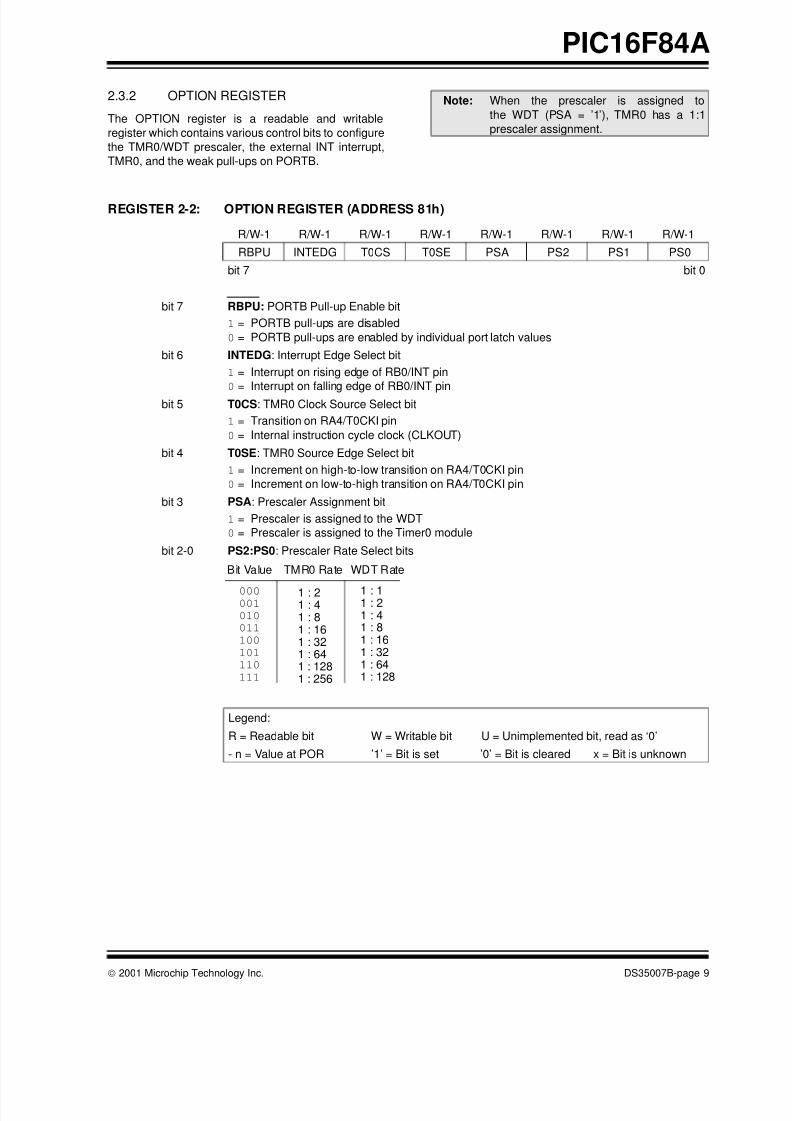
2.3.2 OPTION REGISTER
The OPTION register is a readable and writable
register which contains various control bits to configure
the TMR0/WDT prescaler, the external INT interrupt,
TMR0, and the weak pull-ups on PORTB.
REGISTER 2-2: OPTION REGISTER (ADDRESS 81h)
Note: When the prescaler is assigned to
the WDT (PSA = ’1’), TMR0 has a 1:1
prescaler assignment.
R/W-1 R/W-1 R/W-1 R/W-1 R/W-1 R/W-1 R/W-1 R/W-1
RBPU INTEDG T0CS T0SE PSA PS2 PS1 PS0
bit 7 bit 0
bit 7 RBPU: PORTB Pull-up Enable bit
1 = PORTB pull-ups are disabled
0 = PORTB pull-ups are enabled by individual port latch values
bit 6 INTEDG: Interrupt Edge Select bit
1 = Interrupt on rising edge of RB0/INT pin
0 = Interrupt on falling edge of RB0/INT pin
bit 5 T0CS: TMR0 Clock Source Select bit
1 = Transition on RA4/T0CKI pin
0 = Internal instruction cycle clock (CLKOUT)
bit 4 T0SE: TMR0 Source Edge Select bit
1 = Increment on high-to-low transition on RA4/T0CKI pin
0 = Increment on low-to-high transition on RA4/T0CKI pin
bit 3 PSA: Prescaler Assignment bit
1 = Prescaler is assigned to the WDT
0 = Prescaler is assigned to the Timer0 module
bit 2-0 PS2:PS0: Prescaler Rate Select bits
Legend:
R = Readable bit W = Writable bit U = Unimplemented bit, read as ‘0’
- n = Value at POR ’1’ = Bit is set ’0’ = Bit is cleared x = Bit is unknown
000001
010
011
100
101
110
111
1 : 21 : 41 : 81 : 161 : 321 : 641 : 1281 : 256
1 : 11 : 21 : 41 : 81 : 161 : 321 : 641 : 128
Bit Value TMR0 Rate WDT Rate

8/8/2019 Datasheet PIC16F84A
http://slidepdf.com/reader/full/datasheet-pic16f84a 12/88
PIC16F84A
DS35007B-page 10 2001 Microchip Technology Inc.
2.3.3 INTCON REGISTER
The INTCON register is a readable and writable
register that contains the various enable bits for all
interrupt sources.
REGISTER 2-3: INTCON REGISTER (ADDRESS 0Bh, 8Bh)
Note: Interrupt flag bits are set when an interrupt
condition occurs, regardless of the state of
its corresponding enable bit or the global
enable bit, GIE (INTCON<7>).
R/W-0 R/W-0 R/W-0 R/W-0 R/W-0 R/W-0 R/W-0 R/W-x
GIE EEIE T0IE INTE RBIE T0IF INTF RBIF
bit 7 bit 0
bit 7 GIE: Global Interrupt Enable bit
1 = Enables all unmasked interrupts
0 = Disables all interrupts
bit 6 EEIE: EE Write Complete Interrupt Enable bit
1 = Enables the EE Write Complete interrupts
0 = Disables the EE Write Complete interrupt
bit 5 T0IE: TMR0 Overflow Interrupt Enable bit
1 = Enables the TMR0 interrupt
0 = Disables the TMR0 interrupt
bit 4 INTE: RB0/INT External Interrupt Enable bit
1 = Enables the RB0/INT external interrupt
0 = Disables the RB0/INT external interrupt
bit 3 RBIE: RB Port Change Interrupt Enable bit
1 = Enables the RB port change interrupt
0 = Disables the RB port change interrupt
bit 2 T0IF: TMR0 Overflow Interrupt Flag bit
1 = TMR0 register has overflowed (must be cleared in software)
0 = TMR0 register did not overflow
bit 1 INTF: RB0/INT External Interrupt Flag bit
1 = The RB0/INT external interrupt occurred (must be cleared in software)
0 = The RB0/INT external interrupt did not occur
bit 0 RBIF: RB Port Change Interrupt Flag bit
1 = At least one of the RB7:RB4 pins changed state (must be cleared in software)
0 = None of the RB7:RB4 pins have changed state
Legend:
R = Readable bit W = Writable bit U = Unimplemented bit, read as ‘0’
- n = Value at POR ’1’ = Bit is set ’0’ = Bit is cleared x = Bit is unknown

8/8/2019 Datasheet PIC16F84A
http://slidepdf.com/reader/full/datasheet-pic16f84a 13/88
2001 Microchip Technology Inc. DS35007B-page 11
PIC16F84A
2.4 PCL and PCLATH
The program counter (PC) specifies the address of the
instruction to fetch for execution. The PC is 13 bits
wide. The low byte is called the PCL register. This reg-
ister is readable and writable. The high byte is called
the PCH register. This register contains the PC<12:8>
bits and is not directly readable or writable. If the pro-gram counter (PC) is modified or a conditional test is
true, the instruction requires two cycles. The second
cycle is executed as a NOP. All updates to the PCH reg-
ister go through the PCLATH register.
2.4.1 STACK
The stack allows a combination of up to 8 program calls
and interrupts to occur. The stack contains the return
address from this branch in program execution.
Mid-range devices have an 8 level deep x 13-bit wide
hardware stack. The stack space is not part of either
program or data space and the stack pointer is not
readable or writable. The PC is PUSHed onto the stackwhen a CALL instruction is executed or an interrupt
causes a branch. The stack is POPed in the event of a
RETURN, RETLW or a RETFIE instruction execution.
PCLATH is not modified when the stack is PUSHed or
POPed.
After the stack has been PUSHed eight times, the ninth
push overwrites the value that was stored from the first
push. The tenth push overwrites the second push (and
so on).
2.5 Indirect Addressing; INDF andFSR Registers
The INDF register is not a physical register. Addressing
INDF actually addresses the register whose address is
contained in the FSR register (FSR is a pointer ). This is
indirect addressing.
EXAMPLE 2-1: INDIRECT ADDRESSING
Reading INDF itself indirectly (FSR = 0) will produce00h. Writing to the INDF register indirectly results in a
no-operation (although STATUS bits may be affected).
A simple program to clear RAM locations 20h-2Fh
using indirect addressing is shown in Example 2-2.
EXAMPLE 2-2: HOW TO CLEAR RAM
USING INDIRECTADDRESSING
An effective 9-bit address is obtained by concatenating
the 8-bit FSR register and the IRP bit (STATUS<7>), as
shown in Figure 2-3. However, IRP is not used in the
PIC16F84A.
• Register file 05 contains the value 10h
• Register file 06 contains the value 0Ah
• Load the value 05 into the FSR register
• A read of the INDF register will return the value
of 10h
• Increment the value of the FSR register by one
(FSR = 06)
• A read of the INDF register now will return the
value of 0Ah.
movlw 0x20 ;initialize pointer
movwf FSR ;to RAM
NEXT clrf INDF ;clear INDF register
incf FSR ;inc pointer
btfss FSR,4 ;all done?
goto NEXT ;NO, clear next
CONTINUE
: ;YES, continue

8/8/2019 Datasheet PIC16F84A
http://slidepdf.com/reader/full/datasheet-pic16f84a 14/88
PIC16F84A
DS35007B-page 12 2001 Microchip Technology Inc.
FIGURE 2-3: DIRECT/INDIRECT ADDRESSING
Direct Addressing
RP1 RP0 6 From Opcode 0 IRP 7 (FSR) 0
Indirect Addressing
Bank Select Location Select Bank Select Location Select
00 01
80h
FFh
00h
0Bh
0Ch
7Fh
Bank 0 Bank 1
Note 1: For memory map detail, see Figure 2-2.
2: Maintain as clear for upward compatibility with future products.
3: Not implemented.
4Fh
50h
Data
Memory(1)
(3) (3)
(2) (2)
Addressesmap back toBank 0

8/8/2019 Datasheet PIC16F84A
http://slidepdf.com/reader/full/datasheet-pic16f84a 15/88
2001 Microchip Technology Inc. DS35007B-page 13
PIC16F84A
3.0 DATA EEPROM MEMORY
The EEPROM data memory is readable and writable
during normal operation (full VDD range). This memory
is not directly mapped in the register file space. Instead
it is indirectly addressed through the Special Function
Registers. There are four SFRs used to read and write
this memory. These registers are:
• EECON1
• EECON2 (not a physically implemented register)
• EEDATA
• EEADR
EEDATA holds the 8-bit data for read/write, and
EEADR holds the address of the EEPROM location
being accessed. PIC16F84A devices have 64 bytes of
data EEPROM with an address range from 0h to 3Fh.
The EEPROM data memory allows byte read and write.
A byte write automatically erases the location and
writes the new data (erase before write). The EEPROM
data memory is rated for high erase/write cycles. The
write time is controlled by an on-chip timer. The write-
time will vary with voltage and temperature as well as
from chip to chip. Please refer to AC specifications for
exact limits.
When the device is code protected, the CPU may
continue to read and write the data EEPROM memory.
The device programmer can no longer access
this memory.
Additional information on the Data EEPROM is avail-
able in the PICmicro™ Mid-Range Reference Manual
(DS33023).
REGISTER 3-1: EECON1 REGISTER (ADDRESS 88h)
U-0 U-0 U-0 R/W-0 R/W-x R/W-0 R/S-0 R/S-0 — — — EEIF WRERR WREN WR RD
bit 7 bit 0
bit 7-5 Unimplemented: Read as '0'
bit 4 EEIF: EEPROM Write Operation Interrupt Flag bit
1 = The write operation completed (must be cleared in software)
0 = The write operation is not complete or has not been started
bit 3 WRERR: EEPROM Error Flag bit
1 = A write operation is prematurely terminated
(any MCLR Reset or any WDT Reset during normal operation)
0 = The write operation completed
bit 2 WREN: EEPROM Write Enable bit1 = Allows write cycles
0 = Inhibits write to the EEPROM
bit 1 WR: Write Control bit
1 = Initiates a write cycle. The bit is cleared by hardware once write is complete. The WR bit
can only be set (not cleared) in software.
0 = Write cycle to the EEPROM is complete
bit 0 RD: Read Control bit
1 = Initiates an EEPROM read RD is cleared in hardware. The RD bit can only be set (not
cleared) in software.
0 = Does not initiate an EEPROM read
Legend:R = Readable bit W = Writable bit U = Unimplemented bit, read as ‘0’
- n = Value at POR ’1’ = Bit is set ’0’ = Bit is cleared x = Bit is unknown

8/8/2019 Datasheet PIC16F84A
http://slidepdf.com/reader/full/datasheet-pic16f84a 16/88
PIC16F84A
DS35007B-page 14 2001 Microchip Technology Inc.
3.1 Reading the EEPROM DataMemory
To read a data memory location, the user must write the
address to the EEADR register and then set control bit
RD (EECON1<0>). The data is available, in the very
next cycle, in the EEDATA register; therefore, it can be
read in the next instruction. EEDATA will hold this valueuntil another read or until it is written to by the user
(during a write operation).
EXAMPLE 3-1: DATA EEPROM READ
3.2 Writing to the EEPROM Data
Memory
To write an EEPROM data location, the user must first
write the address to the EEADR register and the data
to the EEDATA register. Then the user must follow a
specific sequence to initiate the write for each byte.
EXAMPLE 3-2: DATA EEPROM WRITE
The write will not initiate if the above sequence is not
exactly followed (write 55h to EECON2, write AAh to
EECON2, then set WR bit) for each byte. We strongly
recommend that interrupts be disabled during this
code segment.
Additionally, the WREN bit in EECON1 must be set to
enable write. This mechanism prevents accidental writes
to data EEPROM due to errant (unexpected) code exe-
cution (i.e., lost programs). The user should keep the
WREN bit clear at all times, except when updating
EEPROM. The WREN bit is not cleared by hardware.
After a write sequence has been initiated, clearing the
WREN bit will not affect this write cycle. The WR bit willbe inhibited from being set unless the WREN bit is set.
At the completion of the write cycle, the WR bit is
cleared in hardware and the EE Write Complete
Interrupt Flag bit (EEIF) is set. The user can either
enable this interrupt or poll this bit. EEIF must be
cleared by software.
3.3 Write Verify
Depending on the application, good programming
practice may dictate that the value written to the Data
EEPROM should be verified (Example 3-3) to the
desired value to be written. This should be used in
applications where an EEPROM bit will be stressednear the specification limit.
Generally, the EEPROM write failure will be a bit which
was written as a ’0’, but reads back as a ’1’ (due to
leakage off the bit).
EXAMPLE 3-3: WRITE VERIFY
TABLE 3-1: REGISTERS/BITS ASSOCIATED WITH DATA EEPROM
BCF STATUS, RP0 ; Bank 0
MOVLW CONFIG_ADDR ;
MOVWF EEADR ; Address to read
BSF STATUS, RP0 ; Bank 1
BSF EECON1, RD ; EE Read
BCF STATUS, RP0 ; Bank 0
MOVF EEDATA, W ; W = EEDATA
BSF STATUS, RP0 ; Bank 1
BCF INTCON, GIE ; Disable INTs.
BSF EECON1, WREN ; Enable Write
MOVLW 55h ;
MOVWF EECON2 ; Write 55h
MOVLW AAh ;
MOVWF EECON2 ; Write AAhBSF EECON1,WR ; Set WR bit
; begin write
BSF INTCON, GIE ; Enable INTs. R e q u i r e d
S e q u e n c e
BCF STATUS,RP0 ; Bank 0
: ; Any code
: ; can go here
MOVF EEDATA,W ; Must be in Bank 0
BSF STATUS,RP0 ; Bank 1
READ
BSF EECON1, RD ; YES, Read the
; value written
BCF STATUS, RP0 ; Bank 0
;
; Is the value written
; (in W reg) and
; read (in EEDATA)
; the same?
;
SUBWFEEDATA, W ;
BTFSS STATUS, Z ; Is difference 0?
GOTO WRITE_ERR ; NO, Write error
Address Name Bit 7 Bit 6 Bit 5 Bit 4 Bit 3 Bit 2 Bit 1 Bit 0Value onPower-on
Reset
Value onall otherRESETS
08h EEDATA EEPROM Data Register xxxx xxxx uuuu uuuu
09h EEADR EEPROM Address Register xxxx xxxx uuuu uuuu
88h EECON1 — — — EEIF WRERR WREN WR RD ---0 x000 ---0 q000
89h EECON2 EEPROM Control Register 2 ---- ---- ---- ----
Legend: x = unknown, u = unchanged, - = unimplemented, read as '0', q = value depends upon condition.
Shaded cells are not used by data EEPROM.

8/8/2019 Datasheet PIC16F84A
http://slidepdf.com/reader/full/datasheet-pic16f84a 17/88
2001 Microchip Technology Inc. DS35007B-page 15
PIC16F84A
4.0 I/O PORTS
Some pins for these I/O ports are multiplexed with an
alternate function for the peripheral features on the
device. In general, when a peripheral is enabled, that
pin may not be used as a general purpose I/O pin.
Additional information on I/O ports may be found in the
PICmicro™ Mid-Range Reference Manual (DS33023).
4.1 PORTA and TRISA Registers
PORTA is a 5-bit wide, bi-directional port. The corre-
sponding data direction register is TRISA. Setting a
TRISA bit (= 1) will make the corresponding PORTA pin
an input (i.e., put the corresponding output driver in a
Hi-Impedance mode). Clearing a TRISA bit (= 0) will
make the corresponding PORTA pin an output (i.e., put
the contents of the output latch on the selected pin).
Reading the PORTA register reads the status of the
pins, whereas writing to it will write to the port latch. All
write operations are read-modify-write operations.
Therefore, a write to a port implies that the port pins are
read. This value is modified and then written to the port
data latch.
Pin RA4 is multiplexed with the Timer0 module clock
input to become the RA4/T0CKI pin. The RA4/T0CKI
pin is a Schmitt Trigger input and an open drain output.
All other RA port pins have TTL input levels and full
CMOS output drivers.
EXAMPLE 4-1: INITIALIZING PORTA
FIGURE 4-1: BLOCK DIAGRAM OF
PINS RA3:RA0
FIGURE 4-2: BLOCK DIAGRAM OF PIN
RA4
Note: On a Power-on Reset, these pins are con-
figured as inputs and read as '0'.
BCF STATUS, RP0 ;
CLRF PORTA ; Initialize PORTA by
; clearing output
; data latches
BSF STATUS, RP0 ; Select Bank 1
MOVLW 0x0F ; Value used to
; initialize data
; direction
MOVWF TRISA ; Set RA<3:0> as inputs
; RA4 as output
; TRISA<7:5> are always
; read as ’0’.
DataBus
QD
QCK
QD
QCK
Q D
EN
P
N
WRPort
WRTRIS
Data Latch
TRIS Latch
RD TRIS
RD Port
TTLInputBuffer
VSS
VDD
I/O pin
Note: I/O pins have protection diodes to VDD and VSS.
Data
BusWRPort
WRTRIS
RD Port
Data Latch
TRIS Latch
RD TRIS
SchmittTriggerInputBuffer
N
VSS
RA4 pin
TMR0 Clock Input
QD
QCK
QD
QCK
EN
Q D
EN
Note: I/O pins have protection diodes to VDD and VSS.

8/8/2019 Datasheet PIC16F84A
http://slidepdf.com/reader/full/datasheet-pic16f84a 18/88
PIC16F84A
DS35007B-page 16 2001 Microchip Technology Inc.
TABLE 4-1: PORTA FUNCTIONS
TABLE 4-2: SUMMARY OF REGISTERS ASSOCIATED WITH PORTA
Name Bit0 Buffer Type Function
RA0 bit0 TTL Input/output
RA1 bit1 TTL Input/output
RA2 bit2 TTL Input/output
RA3 bit3 TTL Input/outputRA4/T0CKI bit4 ST Input/output or external clock input for TMR0.
Output is open drain type.
Legend: TTL = TTL input, ST = Schmitt Trigger input
Address Name Bit 7 Bit 6 Bit 5 Bit 4 Bit 3 Bit 2 Bit 1 Bit 0
Value on
Power-on
Reset
Value on all
other
RESETS
05h PORTA — — — RA4/T0CKI RA3 RA2 RA1 RA0 ---x xxxx ---u uuuu
85h TRISA — — — TRISA4 TRISA3 TRISA2 TRISA1 TRISA0 ---1 1111 ---1 1111
Legend: x = unknown, u = unchanged, - = unimplemented, read as '0'. Shaded cells are unimplemented, read as '0'.

8/8/2019 Datasheet PIC16F84A
http://slidepdf.com/reader/full/datasheet-pic16f84a 19/88
2001 Microchip Technology Inc. DS35007B-page 17
PIC16F84A
4.2 PORTB and TRISB Registers
PORTB is an 8-bit wide, bi-directional port. The corre-
sponding data direction register is TRISB. Setting a
TRISB bit (= 1) will make the corresponding PORTB pin
an input (i.e., put the corresponding output driver in a
Hi-Impedance mode). Clearing a TRISB bit (= 0) will
make the corresponding PORTB pin an output (i.e., putthe contents of the output latch on the selected pin).
EXAMPLE 4-2: INITIALIZING PORTB
Each of the PORTB pins has a weak internal pull-up. A
single control bit can turn on all the pull-ups. This is per-
formed by clearing bit RBPU (OPTION<7>). The weak
pull-up is automatically turned off when the port pin is
configured as an output. The pull-ups are disabled on a
Power-on Reset.
Four of PORTB’s pins, RB7:RB4, have an interrupt-on-
change feature. Only pins configured as inputs can
cause this interrupt to occur (i.e., any RB7:RB4 pin
configured as an output is excluded from the interrupt-
on-change comparison). The input pins (of RB7:RB4)
are compared with the old value latched on the last
read of PORTB. The “mismatch” outputs of RB7:RB4are OR’ed together to generate the RB Port Change
Interrupt with flag bit RBIF (INTCON<0>).
This interrupt can wake the device from SLEEP. The
user, in the Interrupt Service Routine, can clear the
interrupt in the following manner:
a) Any read or write of PORTB. This will end the
mismatch condition.
b) Clear flag bit RBIF.
A mismatch condition will continue to set flag bit RBIF.
Reading PORTB will end the mismatch condition and
allow flag bit RBIF to be cleared.
The interrupt-on-change feature is recommended for
wake-up on key depression operation and operations
where PORTB is only used for the interrupt-on-change
feature. Polling of PORTB is not recommended while
using the interrupt-on-change feature.
FIGURE 4-3: BLOCK DIAGRAM OF
PINS RB7:RB4
FIGURE 4-4: BLOCK DIAGRAM OF
PINS RB3:RB0
BCF STATUS, RP0 ;
CLRF PORTB ; Initialize PORTB by
; clearing output
; data latches
BSF STATUS, RP0 ; Select Bank 1
MOVLW 0xCF ; Value used to
; initialize data
; direction
MOVWF TRISB ; Set RB<3:0> as inputs
; RB<5:4> as outputs
; RB<7:6> as inputs
RBPU(1)
Data Latch
From other
P
VDD
QD
CK
QD
CK
Q D
EN
Q D
EN
Data Bus
WR Port
WR TRIS
Set RBIF
TRIS Latch
RD TRIS
RD Port
RB7:RB4 pins
WeakPull-up
RD Port
Latch
TTLInputBuffer
Note 1: TRISB = ’1’ enables weak pull-up(if RBPU = ’0’ in the OPTION_REG register).
2: I/O pins have diode protection to VDD and VSS.
I/O pin(2)
RBPU(1)
I/O pin(2)
Data Latch
P
VDD
QD
CK
QD
CK
Q D
EN
Data Bus
WR Port
WR TRIS
RD TRIS
RD Port
WeakPull-up
RD Port
RB0/INT
TTLInputBuffer
Schmitt TriggerBuffer
TRIS Latch
Note 1: TRISB = ’1’ enables weak pull-up(if RBPU = ’0’ in the OPTION_REG register).
2: I/O pins have diode protection to VDD and VSS.

8/8/2019 Datasheet PIC16F84A
http://slidepdf.com/reader/full/datasheet-pic16f84a 20/88
PIC16F84A
DS35007B-page 18 2001 Microchip Technology Inc.
TABLE 4-3: PORTB FUNCTIONS
TABLE 4-4: SUMMARY OF REGISTERS ASSOCIATED WITH PORTB
Name Bit Buffer Type I/O Consistency Function
RB0/INT bit0 TTL/ST(1) Input/output pin or external interrupt input.
Internal software programmable weak pull-up.
RB1 bit1 TTL Input/output pin. Internal software programmable weak pull-up.
RB2 bit2 TTL Input/output pin. Internal software programmable weak pull-up.RB3 bit3 TTL Input/output pin. Internal software programmable weak pull-up.
RB4 bit4 TTL Input/output pin (with interrupt-on-change).
Internal software programmable weak pull-up.
RB5 bit5 TTL Input/output pin (with interrupt-on-change).
Internal software programmable weak pull-up.
RB6 bit6 TTL/ST(2) Input/output pin (with interrupt-on-change).
Internal software programmable weak pull-up. Serial programming clock.
RB7 bit7 TTL/ST(2) Input/output pin (with interrupt-on-change).
Internal software programmable weak pull-up. Serial programming data.
Legend: TTL = TTL input, ST = Schmitt Trigger.
Note 1: This buffer is a Schmitt Trigger input when configured as the external interrupt.
2: This buffer is a Schmitt Trigger input when used in Serial Programming mode.
Address Name Bit 7 Bit 6 Bit 5 Bit 4 Bit 3 Bit 2 Bit 1 Bit 0
Value on
Power-on
Reset
Value on
all other
RESETS
06h PORTB RB7 RB6 RB5 RB4 RB3 RB2 RB1 RB0/INT xxxx xxxx uuuu uuuu
86h TRISB TRISB7 TRISB6 TRISB5 TRISB4 TRISB3 TRISB2 TRISB1 TRISB0 1111 1111 1111 1111
81h OPTION_REG RBPU INTEDG T0CS T0SE PSA PS2 PS1 PS0 1111 1111 1111 1111
0Bh,8Bh INTCON GIE EEIE T0IE INTE RBIE T0IF INTF RBIF 0000 000x 0000 000u
Legend: x = unknown, u = unchanged. Shaded cells are not used by PORTB.

8/8/2019 Datasheet PIC16F84A
http://slidepdf.com/reader/full/datasheet-pic16f84a 21/88
2001 Microchip Technology Inc. DS35007B-page 19
PIC16F84A
5.0 TIMER0 MODULE
The Timer0 module timer/counter has the following
features:
• 8-bit timer/counter
• Readable and writable
• Internal or external clock select
• Edge select for external clock
• 8-bit software programmable prescaler
• Interrupt-on-overflow from FFh to 00h
Figure 5-1 is a simplified block diagram of the Timer0
module.
Additional information on timer modules is available in
the PICmicro™ Mid-Range Reference Manual
(DS33023).
5.1 Timer0 Operation
Timer0 can operate as a timer or as a counter.
Timer mode is selected by clearing bit T0CS(OPTION_REG<5>). In Timer mode, the Timer0 mod-
ule will increment every instruction cycle (without pres-
caler). If the TMR0 register is written, the increment is
inhibited for the following two instruction cycles. The
user can work around this by writing an adjusted value
to the TMR0 register.
Counter mode is selected by setting bit T0CS
(OPTION_REG<5>). In Counter mode, Timer0 will
increment, either on every rising or falling edge of pin
RA4/T0CKI. The incrementing edge is determined by
the Timer0 Source Edge Select bit, T0SE
(OPTION_REG<4>). Clearing bit T0SE selects the ris-
ing edge. Restrictions on the external clock input are
discussed below.
When an external clock input is used for Timer0, it must
meet certain requirements. The requirements ensure
the external clock can be synchronized with the internal
phase clock (TOSC). Also, there is a delay in the actual
incrementing of Timer0 after synchronization.
Additional information on external clock requirements
is available in the PICmicro™ Mid-Range Reference
Manual, (DS33023).
5.2 Prescaler
An 8-bit counter is available as a prescaler for the Timer0
module, or as a postscaler for the Watchdog Timer,
respectively (Figure 5-2). For simplicity, this counter is
being referred to as “prescaler” throughout this data
sheet. Note that there is only one prescaler available
which is mutually exclusively shared between the Timer0
module and the Watchdog Timer. Thus, a prescaler
assignment for the Timer0 module means that there is no
prescaler for the Watchdog Timer, and vice-versa.
The prescaler is not readable or writable.
The PSA and PS2:PS0 bits (OPTION_REG<3:0>)
determine the prescaler assignment and prescale ratio.
Clearing bit PSA will assign the prescaler to the Timer0
module. When the prescaler is assigned to the Timer0
module, prescale values of 1:2, 1:4, ..., 1:256 are
selectable.
Setting bit PSA will assign the prescaler to the Watchdog
Timer (WDT). When the prescaler is assigned to the
WDT, prescale values of 1:1, 1:2, ..., 1:128 are selectable.
When assigned to the Timer0 module, all instructions
writing to the TMR0 register (e.g., CLRF 1, MOVWF 1,
BSF 1,etc.) will clear the prescaler. When assigned to
WDT, a CLRWDT instruction will clear the prescaleralong with the WDT.
FIGURE 5-1: TIMER0 BLOCK DIAGRAM
Note: Writing to TMR0 when the prescaler is
assigned to Timer0 will clear the prescaler
count, but will not change the prescaler
assignment.
Note 1: T0CS, T0SE, PSA, PS2:PS0 (OPTION_REG<5:0>).
2: The prescaler is shared with Watchdog Timer (refer to Figure 5-2 for detailed block diagram).
RA4/T0CKI
T0SE
0
1
1
0pin
T0CS
FOSC /4
ProgrammablePrescaler
Sync withInternalClocks
TMR0
PSOUT
(2 Cycle Delay)
PSOUT
Data Bus
8
PSAPS2, PS1, PS0Set InterruptFlag bit T0IFon Overflow
3

8/8/2019 Datasheet PIC16F84A
http://slidepdf.com/reader/full/datasheet-pic16f84a 22/88
PIC16F84A
DS35007B-page 20 2001 Microchip Technology Inc.
5.2.1 SWITCHING PRESCALER
ASSIGNMENT
The prescaler assignment is fully under software con-
trol (i.e., it can be changed “on the fly” during program
execution).
5.3 Timer0 Interrupt
The TMR0 interrupt is generated when the TMR0 reg-
ister overflows from FFh to 00h. This overflow sets bit
T0IF (INTCON<2>). The interrupt can be masked by
clearing bit T0IE (INTCON<5>). Bit T0IF must be
cleared in software by the Timer0 module Interrupt Ser-
vice Routine before re-enabling this interrupt. TheTMR0 interrupt cannot awaken the processor from
SLEEP since the timer is shut-off during SLEEP.
FIGURE 5-2: BLOCK DIAGRAM OF THE TIMER0/WDT PRESCALER
TABLE 5-1: REGISTERS ASSOCIATED WITH TIMER0
Note: To avoid an unintended device RESET, a
specific instruction sequence (shown in thePICmicro™ Mid-Range Reference Man-
ual, DS33023) must be executed when
changing the prescaler assignment from
Timer0 to the WDT. This sequence must
be followed even if the WDT is disabled.
RA4/T0CKI
T0SE
pin
M
UX
CLKOUT (= FOSC /4)
SYNC2
CyclesTMR0 reg
8-bit Prescaler
8 - to - 1 MUX
M
UX
M U X
WatchdogTimer
PSA
0 1
0
1
WDTTime-out
PS2:PS0
8
Note: T0CS, T0SE, PSA, PS2:PS0 are (OPTION_REG<5:0>).
PSA
WDT Enable bit
MUX
0
1 0
1
Data Bus
Set Flag bit T0IFon Overflow
8
PSAT0CS
Address Name Bit 7 Bit 6 Bit 5 Bit 4 Bit 3 Bit 2 Bit 1 Bit 0
Value on
POR,
BOR
Value on all
other
RESETS
01h TMR0 Timer0 Module Register xxxx xxxx uuuu uuuu
0Bh,8Bh INTCON GIE EEIE T0IE INTE RBIE T0IF INTF RBIF 0000 000x 0000 000u
81h OPTION_REG RBPU INTEDG T0CS T0SE PSA PS2 PS1 PS0 1111 1111 1111 1111
85h TRISA — — — PORTA Data Direction Register ---1 1111 ---1 1111
Legend: x = unknown, u = unchanged, - = unimplemented locations read as '0'. Shaded cells are not used by Timer0.

8/8/2019 Datasheet PIC16F84A
http://slidepdf.com/reader/full/datasheet-pic16f84a 23/88
2001 Microchip Technology Inc. DS35007B-page 21
PIC16F84A
6.0 SPECIAL FEATURES OF THECPU
What sets a microcontroller apart from other
processors are special circuits to deal with the needs of
real time applications. The PIC16F84A has a host of
such features intended to maximize system reliability,
minimize cost through elimination of externalcomponents, provide power saving operating modes
and offer code protection. These features are:
• OSC Selection
• RESET
- Power-on Reset (POR)
- Power-up Timer (PWRT)
- Oscillator Start-up Timer (OST)
• Interrupts
• Watchdog Timer (WDT)
• SLEEP
• Code Protection
• ID Locations• In-Circuit Serial Programming™ (ICSP™)
The PIC16F84A has a Watchdog Timer which can be
shut-off only through configuration bits. It runs off its
own RC oscillator for added reliability. There are two
timers that offer necessary delays on power-up. One is
the Oscillator Start-up Timer (OST), intended to keep
the chip in RESET until the crystal oscillator is stable.
The other is the Power-up Timer (PWRT), which pro-
vides a fixed delay of 72 ms (nominal) on power-up
only. This design keeps the device in RESET while the
power supply stabilizes. With these two timers on-chip,
most applications need no external RESET circuitry.
SLEEP mode offers a very low current power-down
mode. The user can wake-up from SLEEP throughexternal RESET, Watchdog Timer Time-out or through
an interrupt. Several oscillator options are provided to
allow the part to fit the application. The RC oscillator
option saves system cost while the LP crystal option
saves power. A set of configuration bits are used to
select the various options.
Additional information on special features is available
in the PICmicro™ Mid-Range Reference Manual
(DS33023).
6.1 Configuration Bits
The configuration bits can be programmed (read as '0'),
or left unprogrammed (read as '1'), to select variousdevice configurations. These bits are mapped in
program memory location 2007h.
Address 2007h is beyond the user program memory
space and it belongs to the special test/configuration
memory space (2000h - 3FFFh). This space can only
be accessed during programming.
REGISTER 6-1: PIC16F84A CONFIGURATION WORD
R/P-u R/P-u R/P-u R/P-u R/P-u R/P-u R/P-u R/P-u R/P-u R/P-u R/P-u R/P-u R/P-u R/P-u
CP CP CP CP CP CP CP CP CP CP PWRTE WDTE F0SC1 F0SC0
bit13 bit0
bit 13-4 CP: Code Protection bit
1 = Code protection disabled
0 = All program memory is code protected
bit 3 PWRTE: Power-up Timer Enable bit
1 = Power-up Timer is disabled
0 = Power-up Timer is enabled
bit 2 WDTE: Watchdog Timer Enable bit
1 = WDT enabled
0 = WDT disabled
bit 1-0 FOSC1:FOSC0: Oscillator Selection bits
11 = RC oscillator
10 = HS oscillator
01 = XT oscillator
00 = LP oscillator

8/8/2019 Datasheet PIC16F84A
http://slidepdf.com/reader/full/datasheet-pic16f84a 24/88
PIC16F84A
DS35007B-page 22 2001 Microchip Technology Inc.
6.2 Oscillator Configurations
6.2.1 OSCILLATOR TYPES
The PIC16F84A can be operated in four different
oscillator modes. The user can program two
configuration bits (FOSC1 and FOSC0) to select one of
these four modes:
• LP Low Power Crystal
• XT Crystal/Resonator
• HS High Speed Crystal/Resonator
• RC Resistor/Capacitor
6.2.2 CRYSTAL OSCILLATOR/CERAMIC
RESONATORS
In XT, LP, or HS modes, a crystal or ceramic resonator
is connected to the OSC1/CLKIN and OSC2/CLKOUT
pins to establish oscillation (Figure 6-1).
FIGURE 6-1: CRYSTAL/CERAMIC
RESONATOR OPERATION(HS, XT OR LP OSCCONFIGURATION)
The PIC16F84A oscillator design requires the use of a
parallel cut crystal. Use of a series cut crystal may give
a frequency out of the crystal manufacturers
specifications. When in XT, LP, or HS modes, the
device can have an external clock source to drive the
OSC1/CLKIN pin (Figure 6-2).
FIGURE 6-2: EXTERNAL CLOCK INPUTOPERATION (HS, XT OR
LP OSCCONFIGURATION)
TABLE 6-1: CAPACITOR SELECTION FORCERAMIC RESONATORS
Note 1: See Table 6-1 for recommended values
of C1 and C2.
2: A series resistor (RS) may be required
for AT strip cut crystals.
C1(1)
C2(1)
XTAL
OSC2
OSC1
RF(3)
SLEEP
To
Logic
PIC16FXXRS
(2)
Internal
Ranges Tested:
Mode Freq OSC1/C1 OSC2/C2
XT 455 kHz
2.0 MHz
4.0 MHz
47 - 100 pF
15 - 33 pF
15 - 33 pF
47 - 100 pF
15 - 33 pF
15 - 33 pF
HS 8.0 MHz
10.0 MHz
15 - 33 pF
15 - 33 pF
15 - 33 pF
15 - 33 pF
Note: Recommended values of C1 and C2 are
identical to the ranges tested in this table.
Higher capacitance increases the stability
of the oscillator, but also increases the
start-up time. These values are for design
guidance only. Since each resonator has
its own characteristics, the user should
consult the resonator manufacturer for the
appropriate values of external compo-
nents.
Note: When using resonators with frequencies
above 3.5 MHz, the use of HS mode rather
than XT mode, is recommended. HS mode
may be used at any VDD for which the
controller is rated.
OSC1
OSC2Open
Clock from
Ext. System PIC16FXX

8/8/2019 Datasheet PIC16F84A
http://slidepdf.com/reader/full/datasheet-pic16f84a 25/88
2001 Microchip Technology Inc. DS35007B-page 23
PIC16F84A
TABLE 6-2: CAPACITOR SELECTION
FOR CRYSTAL OSCILLATOR
6.2.3 RC OSCILLATOR
For timing insensitive applications, the RC device
option offers additional cost savings. The RC oscillator
frequency is a function of the supply voltage, the
resistor (REXT) values, capacitor (CEXT) values, and
the operating temperature. In addition to this, the oscil-
lator frequency will vary from unit to unit due to normal
process parameter variation. Furthermore, the
difference in lead frame capacitance between package
types also affects the oscillation frequency, especially
for low CEXT values. The user needs to take into
account variation, due to tolerance of the external
R and C components. Figure 6-3 shows how an R/C
combination is connected to the PIC16F84A.
FIGURE 6-3: RC OSCILLATOR MODE
Mode Freq OSC1/C1 OSC2/C2
LP 32 kHz
200 kHz
68 - 100 pF
15 - 33 pF
68 - 100 pF
15 - 33 pF
XT 100 kHz
2 MHz
4 MHz
100 - 150 pF
15 - 33 pF
15 - 33 pF
100 - 150 pF
15 - 33 pF
15 - 33 pF
HS 4 MHz
20 MHz
15 - 33 pF
15 - 33 pF
15 - 33 pF
15 - 33 pF
Note: Higher capacitance increases the stability
of the oscillator, but also increases the
start-up time. These values are for design
guidance only. Rs may be required in HS
mode, as well as XT mode, to avoid over-
driving crystals with low drive level specifi-
cation. Since each crystal has its own
characteristics, the user should consult the
crystal manufacturer for appropriate
values of external components.For VDD > 4.5V, C1 = C2 ≈ 30 pF is recom-
mended.
OSC2/CLKOUT
CEXT
REXT
PIC16FXX
OSC1
FOSC /4
Internal
Clock
VDD
VSS
Recommended values: 5 kΩ ≤ REXT ≤ 100 kΩCEXT > 20pF

8/8/2019 Datasheet PIC16F84A
http://slidepdf.com/reader/full/datasheet-pic16f84a 26/88
PIC16F84A
DS35007B-page 24 2001 Microchip Technology Inc.
6.3 RESET
The PIC16F84A differentiates between various kinds
of RESET:
• Power-on Reset (POR)
• MCLR during normal operation
• MCLR during SLEEP
• WDT Reset (during normal operation)• WDT Wake-up (during SLEEP)
Figure 6-4 shows a simplified block diagram of the
On-Chip RESET Circuit. The MCLR Reset path has a
noise filter to ignore small pulses. The electrical speci-
fications state the pulse width requirements for the
MCLR pin.
Some registers are not affected in any RESET condition;
their status is unknown on a POR and unchanged in any
other RESET. Most other registers are reset to a “RESET
state” on POR, MCLR or WDT Reset during normal oper-
ation and on MCLR during SLEEP. They are not affected
by a WDT Reset during SLEEP, since this RESET is
viewed as the resumption of normal operation.
Table 6-3 gives a description of RESET conditions for
the program counter (PC) and the STATUS register.
Table 6-4 gives a full description of RESET states for all
registers.
The TO and PD bits are set or cleared differently in dif-
ferent RESET situations (Section 6.7). These bits are
used in software to determine the nature of the RESET.
FIGURE 6-4: SIMPLIFIED BLOCK DIAGRAM OF ON-CHIP RESET CIRCUIT
TABLE 6-3: RESET CONDITION FOR PROGRAM COUNTER AND THE STATUS REGISTER
S
R Q
External Reset
MCLR
VDD
OSC1/
WDTModule
VDD RiseDetect
OST/PWRT
On-ChipRC Osc(1)
WDT
Time-out
Power-on Reset
OST
10-bit Ripple Counter
PWRT
Chip_Reset
10-bit Ripple Counter
Reset
Enable OST
Enable PWRT
SLEEP
CLKIN
Note 1: This is a separate oscillator from the RC oscillator of the CLKIN pin.
2: See Table 6-5.
See Table 6-5
Condition Program Counter STATUS Register
Power-on Reset 000h0001 1xxx
MCLR during normal operation 000h 000u uuuu
MCLR during SLEEP 000h 0001 0uuu
WDT Reset (during normal operation) 000h 0000 1uuu
WDT Wake-up PC + 1 uuu0 0uuu
Interrupt wake-up from SLEEP PC + 1(1) uuu1 0uuu
Legend: u = unchanged, x = unknown
Note 1: When the wake-up is due to an interrupt and the GIE bit is set, the PC is loaded with the interrupt vector (0004h).

8/8/2019 Datasheet PIC16F84A
http://slidepdf.com/reader/full/datasheet-pic16f84a 27/88
2001 Microchip Technology Inc. DS35007B-page 25
PIC16F84A
TABLE 6-4: RESET CONDITIONS FOR ALL REGISTERS
Register Address Power-on Reset
MCLR during:
– normal operation
– SLEEP
WDT Reset during
normal operation
Wake-up from SLEEP:
– through interrupt
– through WDT Time-out
W — xxxx xxxx uuuu uuuu uuuu uuuu
INDF 00h ---- ---- ---- ---- ---- ----
TMR0 01h xxxx xxxx uuuu uuuu uuuu uuuu
PCL 02h 0000 0000 0000 0000 PC + 1(2)
STATUS 03h 0001 1xxx 000q quuu(3) uuuq quuu(3)
FSR 04h xxxx xxxx uuuu uuuu uuuu uuuu
PORTA(4) 05h ---x xxxx ---u uuuu ---u uuuu
PORTB(5) 06h xxxx xxxx uuuu uuuu uuuu uuuu
EEDATA 08h xxxx xxxx uuuu uuuu uuuu uuuu
EEADR 09h xxxx xxxx uuuu uuuu uuuu uuuu
PCLATH 0Ah ---0 0000 ---0 0000 ---u uuuu
INTCON 0Bh 0000 000x 0000 000u uuuu uuuu(1)
INDF 80h ---- ---- ---- ---- ---- ----
OPTION_REG 81h 1111 1111 1111 1111 uuuu uuuu
PCL 82h 0000 0000 0000 0000 PC + 1(2)
STATUS 83h 0001 1xxx 000q quuu(3)
uuuq quuu(3)
FSR 84h xxxx xxxx uuuu uuuu uuuu uuuu
TRISA 85h ---1 1111 ---1 1111 ---u uuuu
TRISB 86h 1111 1111 1111 1111 uuuu uuuu
EECON1 88h ---0 x000 ---0 q000 ---0 uuuu
EECON2 89h ---- ---- ---- ---- ---- ----
PCLATH 8Ah ---0 0000 ---0 0000 ---u uuuu
INTCON 8Bh 0000 000x 0000 000u uuuu uuuu(1)
Legend: u = unchanged, x = unknown, - = unimplemented bit, read as '0', q = value depends on condition
Note 1: One or more bits in INTCON will be affected (to cause wake-up).
2: When the wake-up is due to an interrupt and the GIE bit is set, the PC is loaded with the interrupt vector
(0004h).
3: Table 6-3 lists the RESET value for each specific condition.
4: On any device RESET, these pins are configured as inputs.
5: This is the value that will be in the port output latch.

8/8/2019 Datasheet PIC16F84A
http://slidepdf.com/reader/full/datasheet-pic16f84a 28/88
PIC16F84A
DS35007B-page 26 2001 Microchip Technology Inc.
6.4 Power-on Reset (POR)
A Power-on Reset pulse is generated on-chip when
VDD rise is detected (in the range of 1.2V - 1.7V). To
take advantage of the POR, just tie the MCLR pin
directly (or through a resistor) to VDD. This will
eliminate external RC components usually needed to
create Power-on Reset. A minimum rise time for VDD
must be met for this to operate properly. See Electrical
Specifications for details.
When the device starts normal operation (exits the
RESET condition), device operating parameters (volt-
age, frequency, temperature, etc.) must be met to
ensure operation. If these conditions are not met, the
device must be held in RESET until the operating con-
ditions are met.
For additional information, refer to Application Note
AN607, "Power-up Trouble Shooting ."
The POR circuit does not produce an internal RESET
when VDD declines.
6.5 Power-up Timer (PWRT)
The Power-up Timer (PWRT) provides a fixed 72 ms
nominal time-out (TPWRT) from POR (Figures 6-6
through 6-9). The Power-up Timer operates on an
internal RC oscillator. The chip is kept in RESET as
long as the PWRT is active. The PWRT delay allows
the VDD to rise to an acceptable level (possible excep-
tion shown in Figure 6-9).
A configuration bit, PWRTE, can enable/disable the
PWRT. See Register 6-1 for the operation of the
PWRTE bit for a particular device.
The power-up time delay TPWRT will vary from chip tochip due to VDD, temperature, and process variation.
See DC parameters for details.
6.6 Oscillator Start-up Timer (OST)
The Oscillator Start-up Timer (OST) provides a 1024
oscillator cycle delay (from OSC1 input) after the
PWRT delay ends (Figure 6-6, Figure 6-7, Figure 6-8
and Figure 6-9). This ensures the crystal oscillator or
resonator has started and stabilized.
The OST time-out (TOST) is invoked only for XT, LP and
HS modes and only on Power-on Reset or wake-up
from SLEEP.
When VDD rises very slowly, it is possible that the
TPWRT time-out and TOST time-out will expire before
VDD has reached its final value. In this case
(Figure 6-9), an external Power-on Reset circuit may
be necessary (Figure 6-5).
FIGURE 6-5: EXTERNAL POWER-ONRESET CIRCUIT (FOR
SLOW VDD POWER-UP)
Note 1: External Power-on Reset circuit is required
only if VDD power-up rate is too slow. The
diode D helps discharge the capacitor
quickly when VDD powers down.
2: R < 40 kΩ is recommended to make sure
that voltage drop across R does not exceed0.2V (max leakage current spec on MCLR
pin is 5 µA). A larger voltage drop will
degrade VIH level on the MCLR pin.
3: R1 = 100Ω to 1 kΩ will limit any current flow-
ing into MCLR from external capacitor C, in
the event of a MCLR pin breakdown due to
ESD or EOS.
C
R1
RD
VDD
MCLR
PIC16FXX
VDD

8/8/2019 Datasheet PIC16F84A
http://slidepdf.com/reader/full/datasheet-pic16f84a 29/88
2001 Microchip Technology Inc. DS35007B-page 27
PIC16F84A
FIGURE 6-6: TIME-OUT SEQUENCE ON POWER-UP (MCLR NOT TIED TO VDD): CASE 1
FIGURE 6-7: TIME-OUT SEQUENCE ON POWER-UP (MCLR NOT TIED TO VDD): CASE 2
FIGURE 6-8: TIME-OUT SEQUENCE ON POWER-UP (MCLR TIED TO VDD): FAST VDD RISETIME
TPWRT
TOST
VDD
MCLR
INTERNAL POR
PWRT TIME-OUT
OST TIME-OUT
INTERNAL RESET
VDD
MCLR
INTERNAL POR
PWRT TIME-OUT
OST TIME-OUT
INTERNAL RESET
TPWRT
TOST
VDD
MCLR
INTERNAL POR
TPWRT
TOSTPWRT TIME-OUT
OST TIME-OUT
INTERNAL RESET

8/8/2019 Datasheet PIC16F84A
http://slidepdf.com/reader/full/datasheet-pic16f84a 30/88
PIC16F84A
DS35007B-page 28 2001 Microchip Technology Inc.
FIGURE 6-9: TIME-OUT SEQUENCE ON POWER-UP (MCLR TIED TO VDD):
SLOW VDD RISE TIME
6.7 Time-out Sequence andPower-down Status Bits (TO/PD)
On power-up (Figures 6-6 through 6-9), the time-out
sequence is as follows:
1. PWRT time-out is invoked after a POR has
expired.
2. Then, the OST is activated.
The total time-out will vary based on oscillator configu-
ration and PWRTE configuration bit status. For exam-ple, in RC mode with the PWRT disabled, there will be
no time-out at all.
TABLE 6-5: TIME-OUT IN VARIOUS
SITUATIONS
Since the time-outs occur from the POR pulse, if MCLR
is kept low long enough, the time-outs will expire. Then
bringing MCLR high, execution will begin immediately
(Figure 6-6). This is useful for testing purposes or to
synchronize more than one PIC16F84A device when
operating in parallel.
Table 6-6 shows the significance of the TO and PD bits.
Table 6-3 lists the RESET conditions for some special
registers, while Table 6-4 lists the RESET conditions
for all the registers.
TABLE 6-6: STATUS BITS AND THEIR
SIGNIFICANCE
VDD
MCLR
V1
When VDD rises very slowly, it is possible that the TPWRT time-out and TOST time-out will expire before VDD
has reached its final value. In this example, the chip will reset properly if, and only if, V1 ≥ VDD min.
INTERNAL POR
TPWRT
TOSTPWRT TIME-OUT
OST TIME-OUT
INTERNAL RESET
Oscillator
Configuration
Power-up Wake-up
from
SLEEPPWRT
Enabled
PWRT
Disabled
XT, HS, LP72 ms +
1024TOSC1024TOSC 1024TOSC
RC 72 ms — —
TO PD Condition
1 1 Power-on Reset
0 x Illegal, TO is set on POR
x 0 Illegal, PD is set on POR
0 1 WDT Reset (during normal operation)
0 0 WDT Wake-up
1 1 MCLR during normal operation
1 0 MCLR during SLEEP or interrupt
wake-up from SLEEP

8/8/2019 Datasheet PIC16F84A
http://slidepdf.com/reader/full/datasheet-pic16f84a 31/88
2001 Microchip Technology Inc. DS35007B-page 29
PIC16F84A
6.8 Interrupts
The PIC16F84A has 4 sources of interrupt:
• External interrupt RB0/INT pin
• TMR0 overflow interrupt
• PORTB change interrupts (pins RB7:RB4)
• Data EEPROM write complete interrupt
The interrupt control register (INTCON) records
individual interrupt requests in flag bits. It also contains
the individual and global interrupt enable bits.
The global interrupt enable bit, GIE (INTCON<7>),
enables (if set) all unmasked interrupts or disables (if
cleared) all interrupts. Individual interrupts can be
disabled through their corresponding enable bits in
INTCON register. Bit GIE is cleared on RESET.
The “return from interrupt” instruction, RETFIE, exits
interrupt routine as well as sets the GIE bit, which
re-enables interrupts.
The RB0/INT pin interrupt, the RB port change interrupt
and the TMR0 overflow interrupt flags are contained inthe INTCON register.
When an interrupt is responded to, the GIE bit is
cleared to disable any further interrupt, the return
address is pushed onto the stack and the PC is loaded
with 0004h. For external interrupt events, such as the
RB0/INT pin or PORTB change interrupt, the interrupt
latency will be three to four instruction cycles. The
exact latency depends when the interrupt event occurs.
The latency is the same for both one and two cycle
instructions. Once in the Interrupt Service Routine, the
source(s) of the interrupt can be determined by polling
the interrupt flag bits. The interrupt flag bit(s) must be
cleared in software before re-enabling interrupts to
avoid infinite interrupt requests.
FIGURE 6-10: INTERRUPT LOGIC
6.8.1 INT INTERRUPT
External interrupt on RB0/INT pin is edge triggered:
either rising if INTEDG bit (OPTION_REG<6>) is set,
or falling if INTEDG bit is clear. When a valid edge
appears on the RB0/INT pin, the INTF bit
(INTCON<1>) is set. This interrupt can be disabled by
clearing control bit INTE (INTCON<4>). Flag bit INTF
must be cleared in software via the Interrupt Service
Routine before re-enabling this interrupt. The INT
interrupt can wake the processor from SLEEP
(Section 6.11) only if the INTE bit was set prior to going
into SLEEP. The status of the GIE bit decides whether
the processor branches to the interrupt vector
following wake-up.
6.8.2 TMR0 INTERRUPT
An overflow (FFh → 00h) in TMR0 will set flag bit T0IF
(INTCON<2>). The interrupt can be enabled/disabled
by setting/clearing enable bit T0IE (INTCON<5>)
(Section 5.0).
6.8.3 PORTB INTERRUPT
An input change on PORTB<7:4> sets flag bit RBIF
(INTCON<0>). The interrupt can be enabled/disabled
by setting/clearing enable bit RBIE (INTCON<3>)
(Section 4.2).
6.8.4 DATA EEPROM INTERRUPT
At the completion of a data EEPROM write cycle, flag
bit EEIF (EECON1<4>) will be set. The interrupt can beenabled/disabled by setting/clearing enable bit EEIE
(INTCON<6>) (Section 3.0).Note: Individual interrupt flag bits are set
regardless of the status of their
corresponding mask bit or the GIE bit.
RBIF
RBIE
T0IFT0IE
INTFINTE
GIE
EEIE
Wake-up(If in SLEEP mode)
Interrupt to CPU
EEIF
Note: For a change on the I/O pin to be
recognized, the pulse width must be at
least TCY wide.

8/8/2019 Datasheet PIC16F84A
http://slidepdf.com/reader/full/datasheet-pic16f84a 32/88
PIC16F84A
DS35007B-page 30 2001 Microchip Technology Inc.
6.9 Context Saving During Interrupts
During an interrupt, only the return PC value is saved
on the stack. Typically, users wish to save key register
values during an interrupt (e.g., W register and
STATUS register). This is implemented in software.
The code in Example 6-1 stores and restores the
STATUS and W register’s values. The user definedregisters, W_TEMP and STATUS_TEMP are the tem-
porary storage locations for the W and STATUS
registers values.
Example 6-1 does the following:
a) Stores the W register.
b) Stores the STATUS register in STATUS_TEMP.
c) Executes the Interrupt Service Routine code.
d) Restores the STATUS (and bank select bit)
register.
e) Restores the W register.
EXAMPLE 6-1: SAVING STATUS AND W REGISTERS IN RAM
6.10 Watchdog Timer (WDT)
The Watchdog Timer is a free running On-Chip RC
Oscillator which does not require any external
components. This RC oscillator is separate from the
RC oscillator of the OSC1/CLKIN pin. That means that
the WDT will run even if the clock on the OSC1/CLKIN
and OSC2/CLKOUT pins of the device has beenstopped, for example, by execution of a SLEEP
instruction. During normal operation, a WDT time-out
generates a device RESET. If the device is in SLEEP
mode, a WDT wake-up causes the device to wake-up
and continue with normal operation. The WDT can be
permanently disabled by programming configuration bit
WDTE as a '0' (Section 6.1).
6.10.1 WDT PERIOD
The WDT has a nominal time-out period of 18 ms, (with
no prescaler). The time-out periods vary with
temperature, VDD and process variations from part to
part (see DC specs). If longer time-out periods are
desired, a prescaler with a division ratio of up to 1:128
can be assigned to the WDT under software control bywriting to the OPTION_REG register. Thus, time-out
periods up to 2.3 seconds can be realized.
The CLRWDT and SLEEP instructions clear the WDT
and the postscaler (if assigned to the WDT) and pre-
vent it from timing out and generating a device
RESETcondition.
The TO bit in the STATUS register will be cleared upon
a WDT time-out.
PUSH MOVWF W_TEMP ; Copy W to TEMP register,
SWAPF STATUS, W ; Swap status to be saved into W
MOVWF STATUS_TEMP ; Save status to STATUS_TEMP register
ISR : :
: ; Interrupt Service Routine
: ; should configure Bank as required
: ;
POP SWAPF STATUS_TEMP,W ; Swap nibbles in STATUS_TEMP register
; and place result into W
MOVWF STATUS ; Move W into STATUS register
; (sets bank to original state)
SWAPF W_TEMP, F ; Swap nibbles in W_TEMP and place result in W_TEMP
SWAPF W_TEMP, W ; Swap nibbles in W_TEMP and place result into W

8/8/2019 Datasheet PIC16F84A
http://slidepdf.com/reader/full/datasheet-pic16f84a 33/88
2001 Microchip Technology Inc. DS35007B-page 31
PIC16F84A
6.10.2 WDT PROGRAMMING
CONSIDERATIONS
It should also be taken into account that under worst
case conditions (VDD = Min., Temperature = Max., Max.
WDT Prescaler), it may take several seconds before a
WDT time-out occurs.
FIGURE 6-11: WATCHDOG TIMER BLOCK DIAGRAM
TABLE 6-7: SUMMARY OF REGISTERS ASSOCIATED WITH THE WATCHDOG TIMER
From TMR0 Clock Source
(Figure 5-2)
To TMR0 (Figure 5-2)
Postscaler
WDT Timer
M
U
X
PSA
8 - to -1 MUX
PSA
WDT
Time-out
10
0
1
WDT
Enable Bit
PS2:PS0
•
•
8
MUX
Note: PSA and PS2:PS0 are bits in the OPTION_REG register.
Addr Name Bit 7 Bit 6 Bit 5 Bit 4 Bit 3 Bit 2 Bit 1 Bit 0
Value on
Power-on
Reset
Value on all
other
RESETS
2007h Config. bits (2) (2) (2) (2) PWRTE(1) WDTE FOSC1 FOSC0 (2)
81h OPTION_REG RBPU INTEDG T0CS T0SE PSA PS2 PS1 PS0 1111 1111 1111 1111
Legend: x = unknown. Shaded cells are not used by the WDT.
Note 1: See Register 6-1 for operation of the PWRTE bit.
2: See Register 6-1 and Section 6.12 for operation of the code and data protection bits.

8/8/2019 Datasheet PIC16F84A
http://slidepdf.com/reader/full/datasheet-pic16f84a 34/88
PIC16F84A
DS35007B-page 32 2001 Microchip Technology Inc.
6.11 Power-down Mode (SLEEP)
A device may be powered down (SLEEP) and later
powered up (wake-up from SLEEP).
6.11.1 SLEEP
The Power-down mode is entered by executing the
SLEEP instruction.
If enabled, the Watchdog Timer is cleared (but keeps
running), the PD bit (STATUS<3>) is cleared, the TO bit
(STATUS<4>) is set, and the oscillator driver is turned
off. The I/O ports maintain the status they had before
the SLEEP instruction was executed (driving high, low,
or hi-impedance).
For the lowest current consumption in SLEEP mode,
place all I/O pins at either VDD or VSS, with no external
circuitry drawing current from the I/O pins, and disable
external clocks. I/O pins that are hi-impedance inputs
should be pulled high or low externally to avoid switch-
ing currents caused by floating inputs. The T0CKI input
should also be at VDD or VSS. The contribution fromon-chip pull-ups on PORTB should be considered.
The MCLR pin must be at a logic high level (VIHMC).
It should be noted that a RESET generated by a WDT
time-out does not drive the MCLR pin low.
6.11.2 WAKE-UP FROM SLEEP
The device can wake-up from SLEEP through one of
the following events:
1. External RESET input on MCLR pin.
2. WDT wake-up (if WDT was enabled).
3. Interrupt from RB0/INT pin, RB port change, or
data EEPROM write complete.
Peripherals cannot generate interrupts during SLEEP,
since no on-chip Q clocks are present.
The first event (MCLR Reset) will cause a device
RESET. The two latter events are considered a contin-
uation of program execution. The TO and PD bits can
be used to determine the cause of a device RESET.
The PD bit, which is set on power-up, is cleared when
SLEEP is invoked. The TO bit is cleared if a WDT
time-out occurred (and caused wake-up).
While the SLEEP instruction is being executed, the next
instruction (PC + 1) is pre-fetched. For the device to
wake-up through an interrupt event, the corresponding
interrupt enable bit must be set (enabled). Wake-up
occurs regardless of the state of the GIE bit. If the GIE
bit is clear (disabled), the device continues execution at
the instruction after the SLEEP instruction. If the GIE bit
is set (enabled), the device executes the instruction
after the SLEEP instruction and then branches to the
interrupt address (0004h). In cases where the
execution of the instruction following SLEEP is not
desirable, the user should have a NOP after the
SLEEP instruction.
FIGURE 6-12: WAKE-UP FROM SLEEP THROUGH INTERRUPT
Q1 Q2 Q3 Q4 Q1 Q2 Q3 Q4 Q1 Q1 Q2 Q3 Q4 Q1 Q2 Q3 Q4 Q1 Q2 Q3 Q4 Q1 Q2 Q3 Q4
OSC1
CLKOUT(4)
INT pin
INTF Flag(INTCON<1>)
GIE bit(INTCON<7>)
INSTRUCTION FLOW
PC
InstructionFetched
InstructionExecuted
PC PC+1 PC+2
Inst(PC) = SLEEP
Inst(PC - 1)
Inst(PC + 1)
SLEEP
Processor in
SLEEP
Interrupt Latency(Note 2)
Inst(PC + 2)
Inst(PC + 1)
Inst(0004h) Inst(0005h)
Inst(0004h)Dummy cycle
PC + 2 0004h 0005h
Dummy cycle
TOST(2)
PC+2
Note 1: XT, HS, or LP oscillator mode assumed.2: TOST = 1024TOSC (drawing not to scale). This delay will not be there for RC osc mode.3: GIE = ’1’ assumed. In this case after wake-up, the processor jumps to the interrupt routine. I f GIE = ’0’, execution will continue in-line.4: CLKOUT is not available in these osc modes, but shown here for timing reference.

8/8/2019 Datasheet PIC16F84A
http://slidepdf.com/reader/full/datasheet-pic16f84a 35/88
2001 Microchip Technology Inc. DS35007B-page 33
PIC16F84A
6.11.3 WAKE-UP USING INTERRUPTS
When global interrupts are disabled (GIE cleared) and
any interrupt source has both its interrupt enable bit
and interrupt flag bit set, one of the following will occur:
• If the interrupt occurs before the execution of a
SLEEP instruction, the SLEEP instruction will com-
plete as a NOP. Therefore, the WDT and WDTpostscaler will not be cleared, the TO bit will not
be set and PD bits will not be cleared.
• If the interrupt occurs during or after the execu-
tion of a SLEEP instruction, the device will imme-
diately wake-up from SLEEP. The SLEEP
instruction will be completely executed before the
wake-up. Therefore, the WDT and WDT
postscaler will be cleared, the TO bit will be set
and the PD bit will be cleared.
Even if the flag bits were checked before executing a
SLEEP instruction, it may be possible for flag bits to
become set before the SLEEP instruction completes. To
determine whether a SLEEP instruction executed, test
the PD bit. If the PD bit is set, the SLEEP instruction
was executed as a NOP.
To ensure that the WDT is cleared, a CLRWDT instruc-
tion should be executed before a SLEEP instruction.
6.12 Program Verification/CodeProtection
If the code protection bit(s) have not been pro-
grammed, the on-chip program memory can be read
out for verification purposes.
6.13 ID LocationsFour memory locations (2000h - 2004h) are designated
as ID locations to store checksum or other code
identification numbers. These locations are not
accessible during normal execution but are readable
and writable only during program/verify. Only the
four Least Significant bits of ID location are usable.
6.14 In-Circuit Serial Programming
PIC16F84A microcontrollers can be serially
programmed while in the end application circuit. This is
simply done with two lines for clock and data, and three
other lines for power, ground, and the programming
voltage. Customers can manufacture boards withunprogrammed devices, and then program the
microcontroller just before shipping the product,
allowing the most recent firmware or custom firmware
to be programmed.
For complete details of Serial Programming, please
refer to the In-Circuit Serial Programming™ (ICSP™)
Guide, (DS30277).

8/8/2019 Datasheet PIC16F84A
http://slidepdf.com/reader/full/datasheet-pic16f84a 36/88
PIC16F84A
DS35007B-page 34 2001 Microchip Technology Inc.
NOTES:

8/8/2019 Datasheet PIC16F84A
http://slidepdf.com/reader/full/datasheet-pic16f84a 37/88

8/8/2019 Datasheet PIC16F84A
http://slidepdf.com/reader/full/datasheet-pic16f84a 38/88
PIC16F84A
DS35007B-page 36 2000 Microchip Technology Inc.
TABLE 7-2: PIC16CXXX INSTRUCTION SET
Mnemonic,
OperandsDescription Cycles
14-Bit Opcode Status
AffectedNotes
MSb LSb
BYTE-ORIENTED FILE REGISTER OPERATIONS
ADDWFANDWF
CLRF
CLRW
COMF
DECF
DECFSZ
INCF
INCFSZ
IORWF
MOVF
MOVWF
NOP
RLF
RRF
SUBWFSWAPF
XORWF
f, df, d
f
-
f, d
f, d
f, d
f, d
f, d
f, d
f, d
f
-
f, d
f, d
f, df, d
f, d
Add W and fAND W with f
Clear f
Clear W
Complement f
Decrement f
Decrement f, Skip if 0
Increment f
Increment f, Skip if 0
Inclusive OR W with f
Move f
Move W to f
No Operation
Rotate Left f through Carry
Rotate Right f through Carry
Subtract W from fSwap nibbles in f
Exclusive OR W with f
11
1
1
1
1
1 (2)
1
1 (2)
1
1
1
1
1
1
11
1
0000
00
00
00
00
00
00
00
00
00
00
00
00
00
0000
00
01110101
0001
0001
1001
0011
1011
1010
1111
0100
1000
0000
0000
1101
1100
00101110
0110
dfffdfff
lfff
0xxx
dfff
dfff
dfff
dfff
dfff
dfff
dfff
lfff
0xx0
dfff
dfff
dfffdfff
dfff
ffffffff
ffff
xxxx
ffff
ffff
ffff
ffff
ffff
ffff
ffff
ffff
0000
ffff
ffff
ffffffff
ffff
C,DC,ZZ
Z
Z
Z
Z
Z
Z
Z
C
C
C,DC,Z
Z
1,21,2
2
1,2
1,2
1,2,3
1,2
1,2,3
1,2
1,2
1,2
1,2
1,21,2
1,2
BIT-ORIENTED FILE REGISTER OPERATIONS
BCF
BSF
BTFSC
BTFSS
f, b
f, b
f, b
f, b
Bit Clear f
Bit Set f
Bit Test f, Skip if Clear
Bit Test f, Skip if Set
1
1
1 (2)
1 (2)
01
01
01
01
00bb
01bb
10bb
11bb
bfff
bfff
bfff
bfff
ffff
ffff
ffff
ffff
1,2
1,2
3
3
LITERAL AND CONTROL OPERATIONS
ADDLW
ANDLW
CALL
CLRWDT
GOTO
IORLWMOVLW
RETFIE
RETLW
RETURN
SLEEP
SUBLW
XORLW
k
k
k
-
k
kk
-
k
-
-
k
k
Add literal and W
AND literal with W
Call subroutine
Clear Watchdog Timer
Go to address
Inclusive OR literal with WMove literal to W
Return from interrupt
Return with literal in W
Return from Subroutine
Go into standby mode
Subtract W from literal
Exclusive OR literal with W
1
1
2
1
2
11
2
2
2
1
1
1
11
11
10
00
10
1111
00
11
00
00
11
11
111x
1001
0kkk
0000
1kkk
100000xx
0000
01xx
0000
0000
110x
1010
kkkk
kkkk
kkkk
0110
kkkk
kkkkkkkk
0000
kkkk
0000
0110
kkkk
kkkk
kkkk
kkkk
kkkk
0100
kkkk
kkkkkkkk
1001
kkkk
1000
0011
kkkk
kkkk
C,DC,Z
Z
TO,PD
Z
TO,PD
C,DC,Z
Z
Note 1: When an I/O register is modified as a function of itself ( e.g., MOVF PORTB, 1), the value used will be that value present
on the pins themselves. For example, if the data latch is ’1’ for a pin configured as input and is driven low by an external
device, the data will be written back with a ’0’.
2: If this instruction is executed on the TMR0 register (and, where applicable, d = 1), the prescaler will be cleared if
assigned to the Timer0 Module.
3: If Program Counter (PC) is modified or a conditional test is true, the instruction requires two cycles. The second cycle is
executed as a NOP.
Note: Additional information on the mid-range instruction set is available in the PICmicro™ Mid-Range MCU
Family Reference Manual (DS33023).

8/8/2019 Datasheet PIC16F84A
http://slidepdf.com/reader/full/datasheet-pic16f84a 39/88
2000 Microchip Technology Inc. DS35007B-page 37
PIC16F84A
7.1 Instruction Descriptions
ADDLW Add Literal and W
Syntax: [label ] ADDLW k
Operands: 0 ≤ k ≤ 255
Operation: (W) + k → (W)Status Affected: C, DC, Z
Description: The contents of the W register
are added to the eight-bit literal ’k’
and the result is placed in the W
register.
ADDWF Add W and f
Syntax: [label ] ADDWF f,d
Operands: 0 ≤ f ≤ 127
d ∈ [0,1]
Operation: (W) + (f) → (destination)
Status Affected: C, DC, Z
Description: Add the contents of the W register
with register ’f’. If ’d’ is 0, the result
is stored in the W register. If ’d’ is
1, the result is stored back in
register ’f’.
ANDLW AND Literal with W
Syntax: [label ] ANDLW k
Operands: 0 ≤ k ≤ 255
Operation: (W) .AND. (k) → (W)
Status Affected: Z
Description: The contents of W register are
AND’ed with the eight-bit literal
'k'. The result is placed in the W
register.
ANDWF AND W with f
Syntax: [label ] ANDWF f,d
Operands: 0 ≤ f ≤ 127
d ∈ [0,1]Operation: (W) .AND. (f) → (destination)
Status Affected: Z
Description: AND the W register with register
'f'. If 'd' is 0, the result is stored in
the W register. If 'd' is 1, the result
is stored back in register 'f'.
BCF Bit Clear f
Syntax: [label ] BCF f,b
Operands: 0 ≤ f ≤ 127
0 ≤ b ≤ 7
Operation: 0 → (f<b>)
Status Affected: None
Description: Bit 'b' in register 'f ' is cleared.
BSF Bit Set f
Syntax: [label ] BSF f,b
Operands: 0 ≤ f ≤ 127
0 ≤ b ≤ 7
Operation: 1 → (f<b>)
Status Affected: None
Description: Bit 'b' in register 'f' is set.
BTFSS Bit Test f, Skip if Set
Syntax: [label ] BTFSS f,b
Operands: 0 ≤ f ≤ 127
0 ≤ b < 7
Operation: skip if (f<b>) = 1
Status Affected: None
Description: If bit 'b' in register 'f' is '0', the next
instruction is executed.
If bit 'b' is '1', then the next instruc-
tion is discarded and a NOP is exe-
cuted instead, making this a 2TCY
instruction.
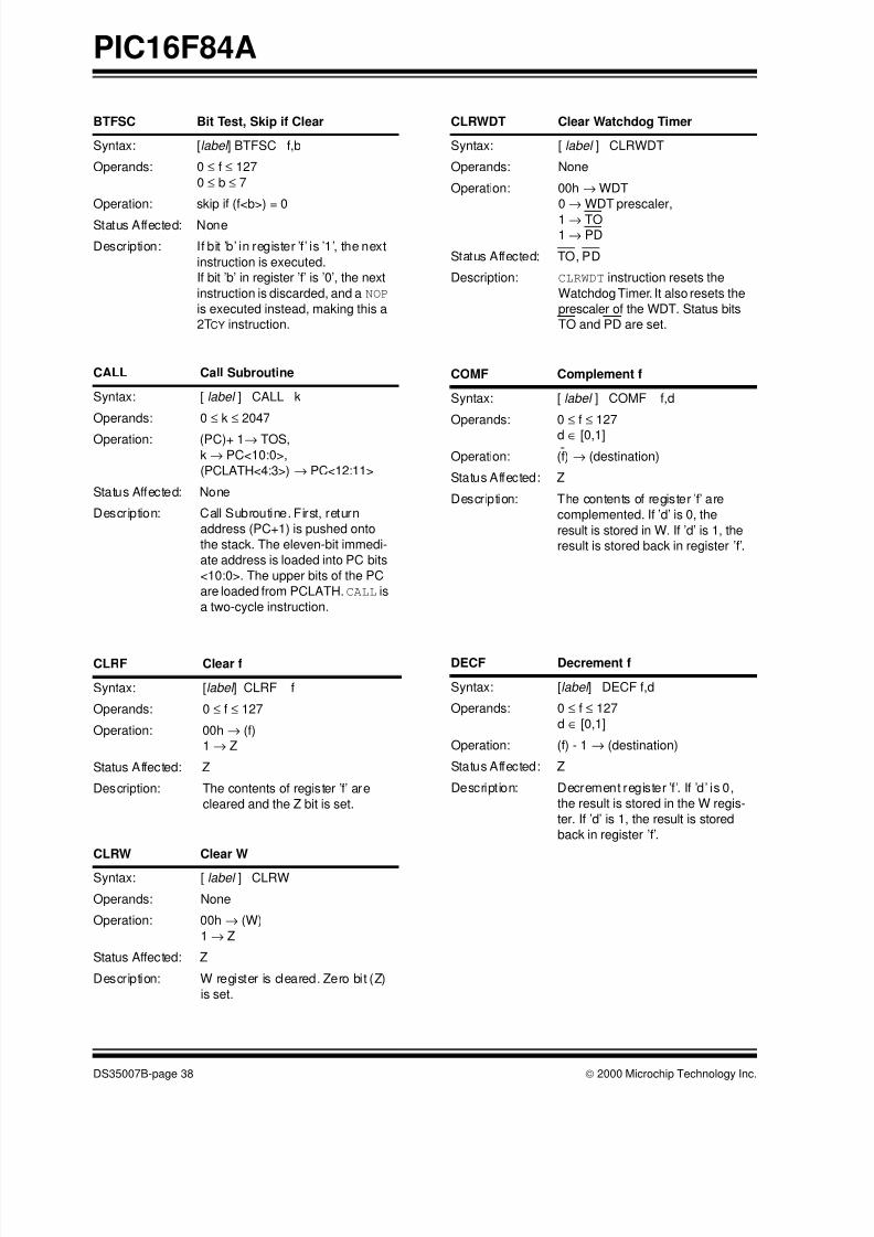
8/8/2019 Datasheet PIC16F84A
http://slidepdf.com/reader/full/datasheet-pic16f84a 40/88
PIC16F84A
DS35007B-page 38 2000 Microchip Technology Inc.
BTFSC Bit Test, Skip if Clear
Syntax: [label ] BTFSC f,b
Operands: 0 ≤ f ≤ 127
0 ≤ b ≤ 7
Operation: skip if (f<b>) = 0
Status Affected: None
Description: If bit ’b’ in register ’f’ is ’1’, the next
instruction is executed.
If bit ’b’ in register ’f’ is ’0’, the next
instruction is discarded, and a NOP
is executed instead, making this a
2TCY instruction.
CALL Call Subroutine
Syntax: [ label ] CALL k
Operands: 0 ≤ k ≤ 2047
Operation: (PC)+ 1→ TOS,
k → PC<10:0>,
(PCLATH<4:3>) → PC<12:11>
Status Affected: None
Description: Call Subroutine. First, return
address (PC+1) is pushed onto
the stack. The eleven-bit immedi-
ate address is loaded into PC bits
<10:0>. The upper bits of the PC
are loaded from PCLATH.CALL is
a two-cycle instruction.
CLRF Clear f
Syntax: [label ] CLRF f
Operands: 0 ≤ f ≤ 127
Operation: 00h → (f)
1 → Z
Status Affected: Z
Description: The contents of register ’f’ are
cleared and the Z bit is set.
CLRW Clear W
Syntax: [ label ] CLRW
Operands: None
Operation: 00h → (W)
1 → Z
Status Affected: Z
Description: W register is cleared. Zero bit (Z)
is set.
CLRWDT Clear Watchdog Timer
Syntax: [ label ] CLRWDT
Operands: None
Operation: 00h → WDT
0 → WDT prescaler,
1 → TO1 → PD
Status Affected: TO, PD
Description: CLRWDT instruction resets the
Watchdog Timer. It also resets the
prescaler of the WDT. Status bits
TO and PD are set.
COMF Complement f
Syntax: [ label ] COMF f,d
Operands: 0 ≤ f ≤ 127
d ∈ [0,1]
Operation: (f) → (destination)
Status Affected: Z
Description: The contents of register ’f’ are
complemented. If ’d’ is 0, the
result is stored in W. If ’d’ is 1, the
result is stored back in register ’f’.
DECF Decrement f
Syntax: [label ] DECF f,d
Operands: 0 ≤ f ≤ 127
d ∈ [0,1]
Operation: (f) - 1 → (destination)
Status Affected: Z
Description: Decrement register ’f ’. If ’d’ is 0,
the result is stored in the W regis-
ter. If ’d’ is 1, the result is stored
back in register ’f’.

8/8/2019 Datasheet PIC16F84A
http://slidepdf.com/reader/full/datasheet-pic16f84a 41/88
2000 Microchip Technology Inc. DS35007B-page 39
PIC16F84A
DECFSZ Decrement f, Skip if 0
Syntax: [ label ] DECFSZ f,d
Operands: 0 ≤ f ≤ 127
d ∈ [0,1]
Operation: (f) - 1 → (destination);
skip if result = 0
Status Affected: None
Description: The contents of register ’f ’ are
decremented. If ’d’ is 0, the result
is placed in the W register. If ’d’ is
1, the result is placed back in
register ’f’.
If the result is 1, the next instruc-
tion is executed. If the result is 0,
then a NOP is executed instead,
making it a 2TCY instruction.
GOTO Unconditional Branch
Syntax: [ label ] GOTO k
Operands: 0 ≤ k ≤ 2047
Operation: k → PC<10:0>
PCLATH<4:3> → PC<12:11>
Status Affected: None
Description: GOTO is an unconditional branch.
The eleven-bit immediate value is
loaded into PC bits <10:0>. The
upper bits of PC are loaded from
PCLATH<4:3>. GOTO is a two-
cycle instruction.
INCF Increment f
Syntax: [ label ] INCF f,d
Operands: 0 ≤ f ≤ 127
d ∈ [0,1]
Operation: (f) + 1 → (destination)
Status Affected: Z
Description: The contents of register ’f ’ are
incremented. If ’d’ is 0, the result
is placed in the W register. If ’d’ is
1, the result is placed back inregister ’f’.
INCFSZ Increment f, Skip if 0
Syntax: [ label ] INCFSZ f,d
Operands: 0 ≤ f ≤ 127
d ∈ [0,1]
Operation: (f) + 1 → (destination),
skip if result = 0
Status Affected: None
Description: The contents of register ’f’ are
incremented. If ’d’ is 0, the result is
placed in the W register. If ’d’ is 1,
the result is placed back in
register ’f’.
If the result is 1, the next instruc-
tion is executed. If the result is 0,
a NOP is executed instead, making
it a 2TCY instruction.
IORLW Inclusive OR Literal with W
Syntax: [ label ] IORLW k
Operands: 0 ≤ k ≤ 255
Operation: (W) .OR. k → (W)
Status Affected: Z
Description: The contents of the W register are
OR’ed with the eight-bit literal 'k'.
The result is placed in the W
register.
IORWF Inclusive OR W with f
Syntax: [ label ] IORWF f,d
Operands: 0 ≤ f ≤ 127
d ∈ [0,1]
Operation: (W) .OR. (f) → (destination)
Status Affected: Z
Description: Inclusive OR the W register with
register 'f'. If 'd' is 0, the result is
placed in the W register. If 'd' is 1,
the result is placed back in
register 'f'.

8/8/2019 Datasheet PIC16F84A
http://slidepdf.com/reader/full/datasheet-pic16f84a 42/88
PIC16F84A
DS35007B-page 40 2000 Microchip Technology Inc.
MOVF Move f
Syntax: [ label ] MOVF f,d
Operands: 0 ≤ f ≤ 127
d ∈ [0,1]
Operation: (f) → (destination)
Status Affected: Z
Description: The contents of register f are
moved to a destination dependant
upon the status of d. If d = 0, des-
tination is W register. If d = 1, the
destination is file register f itself.
d = 1 is useful to test a file register,
since status flag Z is affected.
MOVLW Move Literal to W
Syntax: [ label ] MOVLW k
Operands: 0 ≤ k ≤ 255
Operation: k → (W)
Status Affected: None
Description: The eight-bit li teral ’k’ is loaded
into W register. The don’t cares
will assemble as 0’s.
MOVWF Move W to f
Syntax: [ label ] MOVWF f
Operands: 0 ≤ f ≤ 127
Operation: (W) → (f)
Status Affected: None
Description: Move data from W register to
register 'f'.
NOP No Operation
Syntax: [ label ] NOP
Operands: None
Operation: No operation
Status Affected: None
Description: No operation.
RETFIE Return from Interrupt
Syntax: [ label ] RETFIE
Operands: None
Operation: TOS → PC,
1 → GIE
Status Affected: None
RETLW Return with Literal in W
Syntax: [ label ] RETLW k
Operands: 0 ≤ k ≤ 255
Operation: k → (W);
TOS → PC
Status Affected: None
Description: The W register is loaded with the
eight-bit literal 'k'. The program
counter is loaded from the top of
the stack (the return address).
This is a two-cycle instruction.
RETURN Return from Subroutine
Syntax: [ label ] RETURN
Operands: None
Operation: TOS → PC
Status Affected: None
Description: Return from subroutine. The stack
is POPed and the top of the stack
(TOS) is loaded into the program
counter. This is a two-cycle
instruction.

8/8/2019 Datasheet PIC16F84A
http://slidepdf.com/reader/full/datasheet-pic16f84a 43/88
2000 Microchip Technology Inc. DS35007B-page 41
PIC16F84A
RLF Rotate Left f through Carry
Syntax: [ label ] RLF f,d
Operands: 0 ≤ f ≤ 127
d ∈ [0,1]
Operation: See description below
Status Affected: C
Description: The contents of register ’f’ are
rotated one bit to the left through
the Carry Flag. If ’d’ is 0, the
result is placed in the W register.
If ’d’ is 1, the result is stored back
in register ’f’.
RRF Rotate Right f through Carry
Syntax: [ label ] RRF f,d
Operands: 0 ≤ f ≤ 127
d ∈ [0,1]
Operation: See description below
Status Affected: C
Description: The contents of register ’f’ are
rotated one bit to the right through
the Carry Flag. If ’d’ is 0, the result
is placed in the W register. If ’d’ is
1, the result is placed back in
register ’f’.
SLEEP
Syntax: [ label ] SLEEP
Operands: None
Operation: 00h → WDT,
0 → WDT prescaler,
1 → TO,
0 → PD
Status Affected: TO, PD
Description: The power-down status bi t, PD is
cleared. Time-out status bit, TOis set. Watchdog Timer and its
prescaler are cleared.
The processor is put into SLEEP
mode with the oscillator stopped.
Register fC
Register fC
SUBLW Subtract W from Literal
Syntax: [ label ] SUBLW k
Operands: 0 ≤ k ≤ 255
Operation: k - (W) → (W)
Status Affected: C, DC, ZDescription: The W register is subtracted (2’s
complement method) from the
eight-bit literal 'k'. The result is
placed in the W register.
SUBWF Subtract W from f
Syntax: [ label ] SUBWF f,d
Operands: 0 ≤ f ≤ 127
d ∈ [0,1]
Operation: (f) - (W) → (destination)
Status Affected: C, DC, Z
Description: Subtract (2’s complement method)
W register from register 'f'. If 'd' is 0,
the result is stored in the W regis-
ter. If 'd' is 1, the result is stored
back in register 'f'.
SWAPF Swap Nibbles in f
Syntax: [ label ] SWAPF f,d
Operands: 0 ≤ f ≤ 127
d ∈ [0,1]
Operation: (f<3:0>) → (destination<7:4>),
(f<7:4>) → (destination<3:0>)
Status Affected: None
Description: The upper and lower nibbles of
register 'f' are exchanged. If 'd' is
0, the result is placed in W regis-ter. If 'd' is 1, the result is placed in
register 'f'.

8/8/2019 Datasheet PIC16F84A
http://slidepdf.com/reader/full/datasheet-pic16f84a 44/88
PIC16F84A
DS35007B-page 42 2000 Microchip Technology Inc.
XORLW Exclusive OR Literal with W
Syntax: [label ] XORLW k
Operands: 0 ≤ k ≤ 255
Operation: (W) .XOR. k → (W)
Status Affected: ZDescription: The contents of the W register
are XOR’ed with the eight-bit lit-
eral 'k'. The result is placed in
the W register.
XORWF Exclusive OR W with f
Syntax: [label ] XORWF f,d
Operands: 0 ≤ f ≤ 127
d ∈ [0,1]
Operation: (W) .XOR. (f) → (destination)
Status Affected: Z
Description: Exclusive OR the contents of the
W register with register 'f'. If 'd' is
0, the result is stored in the W
register. If 'd' is 1, the result is
stored back in register 'f'.

8/8/2019 Datasheet PIC16F84A
http://slidepdf.com/reader/full/datasheet-pic16f84a 45/88
2001 Microchip Technology Inc. DS35007B-page 43
PIC16F84A
8.0 DEVELOPMENT SUPPORT
The PICmicro ® microcontrollers are supported with a
full range of hardware and software development tools:
• Integrated Development Environment
- MPLAB ® IDE Software
• Assemblers/Compilers/Linkers
- MPASMTM Assembler
- MPLAB C17 and MPLAB C18 C Compilers
- MPLINKTM Object Linker/
MPLIBTM Object Librarian
• Simulators
- MPLAB SIM Software Simulator
• Emulators
- MPLAB ICE 2000 In-Circuit Emulator
- ICEPIC™ In-Circuit Emulator
• In-Circuit Debugger
- MPLAB ICD
• Device Programmers
- PRO MATE ® II Universal Device Programmer
- PICSTART ® Plus Entry-Level Development
Programmer
• Low Cost Demonstration Boards
- PICDEMTM 1 Demonstration Board
- PICDEM 2 Demonstration Board
- PICDEM 3 Demonstration Board
- PICDEM 17 Demonstration Board
- KEELOQ ® Demonstration Board
8.1 MPLAB Integrated DevelopmentEnvironment Software
The MPLAB IDE software brings an ease of software
development previously unseen in the 8-bit microcon-
troller market. The MPLAB IDE is a Windows ® -based
application that contains:
• An interface to debugging tools
- simulator
- programmer (sold separately)
- emulator (sold separately)
- in-circuit debugger (sold separately)
• A full-featured editor
• A project manager
• Customizable toolbar and key mapping• A status bar
• On-line help
The MPLAB IDE allows you to:
• Edit your source files (either assembly or ‘C’)
• One touch assemble (or compile) and download
to PICmicro emulator and simulator tools (auto-
matically updates all project information)
• Debug using:
- source files- absolute listing file
- machine code
The ability to use MPLAB IDE with multiple debugging
tools allows users to easily switch from the cost-
effective simulator to a full-featured emulator with
minimal retraining.
8.2 MPASM Assembler
The MPASM assembler is a full-featured universal
macro assembler for all PICmicro MCU’s.
The MPASM assembler has a command line interface
and a Windows shell. It can be used as a stand-alone
application on a Windows 3.x or greater system, or it
can be used through MPLAB IDE. The MPASM assem-
bler generates relocatable object files for the MPLINK
object linker, Intel ® standard HEX files, MAP files to
detail memory usage and symbol reference, an abso-
lute LST file that contains source lines and generated
machine code, and a COD file for debugging.
The MPASM assembler features include:
• Integration into MPLAB IDE projects.
• User-defined macros to streamline assembly
code.
• Conditional assembly for multi-purpose source
files.• Directives that allow complete control over the
assembly process.
8.3 MPLAB C17 and MPLAB C18C Compilers
The MPLAB C17 and MPLAB C18 Code Development
Systems are complete ANSI ‘C’ compilers for
Microchip’s PIC17CXXX and PIC18CXXX family of
microcontrollers, respectively. These compilers provide
powerful integration capabilities and ease of use not
found with other compilers.
For easier source level debugging, the compilers pro-
vide symbol information that is compatible with theMPLAB IDE memory display.

8/8/2019 Datasheet PIC16F84A
http://slidepdf.com/reader/full/datasheet-pic16f84a 46/88
PIC16F84A
DS35007B-page 44 2001 Microchip Technology Inc.
8.4 MPLINK Object Linker/MPLIB Object Librarian
The MPLINK object linker combines relocatable
objects created by the MPASM assembler and the
MPLAB C17 and MPLAB C18 C compilers. It can also
link relocatable objects from pre-compiled libraries,
using directives from a linker script.The MPLIB object librarian is a librarian for pre-
compiled code to be used with the MPLINK object
linker. When a routine from a library is called from
another source file, only the modules that contain that
routine will be linked in with the application. This allows
large libraries to be used efficiently in many different
applications. The MPLIB object librarian manages the
creation and modification of library files.
The MPLINK object linker features include:
• Integration with MPASM assembler and MPLAB
C17 and MPLAB C18 C compilers.
• Allows all memory areas to be defined as sections
to provide link-time flexibility.
The MPLIB object librarian features include:
• Easier linking because single libraries can be
included instead of many smaller files.
• Helps keep code maintainable by grouping
related modules together.
• Allows libraries to be created and modules to be
added, listed, replaced, deleted or extracted.
8.5 MPLAB SIM Software Simulator
The MPLAB SIM software simulator allows code devel-
opment in a PC-hosted environment by simulating the
PICmicro series microcontrollers on an instructionlevel. On any given instruction, the data areas can be
examined or modified and stimuli can be applied from
a file, or user-defined key press, to any of the pins. The
execution can be performed in single step, execute
until break, or trace mode.
The MPLAB SIM simulator fully supports symbolic debug-
ging using the MPLAB C17 and the MPLAB C18 C com-
pilers and the MPASM assembler. The software simulator
offers the flexibility to develop and debug code outside of
the laboratory environment, making it an excellent multi-
project software development tool.
8.6 MPLAB ICE High PerformanceUniversal In-Circuit Emulator withMPLAB IDE
The MPLAB ICE universal in-circuit emulator is intended
to provide the product development engineer with a
complete microcontroller design tool set for PICmicro
microcontrollers (MCUs). Software control of theMPLAB ICE in-circuit emulator is provided by the
MPLAB Integrated Development Environment (IDE),
which allows editing, building, downloading and source
debugging from a single environment.
The MPLAB ICE 2000 is a full-featured emulator sys-
tem with enhanced trace, trigger and data monitoring
features. Interchangeable processor modules allow the
system to be easily reconfigured for emulation of differ-
ent processors. The universal architecture of the
MPLAB ICE in-circuit emulator allows expansion to
support new PICmicro microcontrollers.
The MPLAB ICE in-circuit emulator system has been
designed as a real-time emulation system, withadvanced features that are generally found on more
expensive development tools. The PC platform and
Microsoft ® Windows ® environment were chosen to best
make these features available to you, the end user.
8.7 ICEPIC In-Circuit Emulator
The ICEPIC low cost, in-circuit emulator is a solution
for the Microchip Technology PIC16C5X, PIC16C6X,
PIC16C7X and PIC16CXXX families of 8-bit One-
Time-Programmable (OTP) microcontrollers. The mod-
ular system can support different subsets of PIC16C5X
or PIC16CXXX products through the use of inter-
changeable personality modules, or daughter boards.
The emulator is capable of emulating without target
application circuitry being present.

8/8/2019 Datasheet PIC16F84A
http://slidepdf.com/reader/full/datasheet-pic16f84a 47/88
2001 Microchip Technology Inc. DS35007B-page 45
PIC16F84A
8.8 MPLAB ICD In-Circuit Debugger
Microchip’s In-Circuit Debugger, MPLAB ICD, is a pow-
erful, low cost, run-time development tool. This tool is
based on the FLASH PICmicro MCUs and can be used
to develop for this and other PICmicro microcontrollers.
The MPLAB ICD utilizes the in-circuit debugging capa-
bility built into the FLASH devices. This feature, alongwith Microchip’s In-Circuit Serial ProgrammingTM proto-
col, offers cost-effective in-circuit FLASH debugging
from the graphical user interface of the MPLAB
Integrated Development Environment. This enables a
designer to develop and debug source code by watch-
ing variables, single-stepping and setting break points.
Running at full speed enables testing hardware in real-
time.
8.9 PRO MATE II Universal DeviceProgrammer
The PRO MATE II universal device programmer is a
full-featured programmer, capable of operating in
stand-alone mode, as well as PC-hosted mode. ThePRO MATE II device programmer is CE compliant.
The PRO MATE II device programmer has program-
mable VDD and VPP supplies, which allow it to verify
programmed memory at VDD min and VDD max for max-
imum reliability. It has an LCD display for instructions
and error messages, keys to enter commands and a
modular detachable socket assembly to support various
package types. In stand-alone mode, the PRO MATE II
device programmer can read, verify, or program
PICmicro devices. It can also set code protection in this
mode.
8.10 PICSTART Plus Entry LevelDevelopment Programmer
The PICSTART Plus development programmer is an
easy-to-use, low cost, prototype programmer. It con-
nects to the PC via a COM (RS-232) port. MPLAB
Integrated Development Environment software makes
using the programmer simple and efficient.
The PICSTART Plus development programmer sup-
ports all PICmicro devices with up to 40 pins. Larger pin
count devices, such as the PIC16C92X and
PIC17C76X, may be supported with an adapter socket.
The PICSTART Plus development programmer is CE
compliant.
8.11 PICDEM 1 Low Cost PICmicroDemonstration Board
The PICDEM 1 demonstration board is a simple board
which demonstrates the capabilities of several of
Microchip’s microcontrollers. The microcontrollers sup-
ported are: PIC16C5X (PIC16C54 to PIC16C58A),
PIC16C61, PIC16C62X, PIC16C71, PIC16C8X,PIC17C42, PIC17C43 and PIC17C44. All necessary
hardware and software is included to run basic demo
programs. The user can program the sample microcon-
trollers provided with the PICDEM 1 demonstration
board on a PRO MATE II device programmer, or a
PICSTART Plus development programmer, and easily
test firmware. The user can also connect the
PICDEM 1 demonstration board to the MPLAB ICE in-
circuit emulator and download the firmware to the emu-
lator for testing. A prototype area is available for the
user to build some additional hardware and connect it
to the microcontroller socket(s). Some of the features
include an RS-232 interface, a potentiometer for simu-
lated analog input, push button switches and eightLEDs connected to PORTB.
8.12 PICDEM 2 Low Cost PIC16CXXDemonstration Board
The PICDEM 2 demonstration board is a simple dem-
onstration board that supports the PIC16C62,
PIC16C64, PIC16C65, PIC16C73 and PIC16C74
microcontrollers. All the necessary hardware and soft-
ware is included to run the basic demonstration pro-
grams. The user can program the sample
microcontrollers provided with the PICDEM 2 demon-
stration board on a PRO MATE II device programmer,
or a PICSTART Plus development programmer, andeasily test firmware. The MPLAB ICE in-circuit emula-
tor may also be used with the PICDEM 2 demonstration
board to test firmware. A prototype area has been pro-
vided to the user for adding additional hardware and
connecting it to the microcontroller socket(s). Some of
the features include a RS-232 interface, push button
switches, a potentiometer for simulated analog input, a
serial EEPROM to demonstrate usage of the I2CTM
bus and separate headers for connection to an LCD
module and a keypad.

8/8/2019 Datasheet PIC16F84A
http://slidepdf.com/reader/full/datasheet-pic16f84a 48/88
PIC16F84A
DS35007B-page 46 2001 Microchip Technology Inc.
8.13 PICDEM 3 Low Cost PIC16CXXXDemonstration Board
The PICDEM 3 demonstration board is a simple dem-
onstration board that supports the PIC16C923 and
PIC16C924 in the PLCC package. It will also support
future 44-pin PLCC microcontrollers with an LCD Mod-
ule. All the necessary hardware and software isincluded to run the basic demonstration programs. The
user can program the sample microcontrollers pro-
vided with the PICDEM 3 demonstration board on a
PRO MATE II device programmer, or a PICSTART Plus
development programmer with an adapter socket, and
easily test firmware. The MPLAB ICE in-circuit emula-
tor may also be used with the PICDEM 3 demonstration
board to test firmware. A prototype area has been pro-
vided to the user for adding hardware and connecting it
to the microcontroller socket(s). Some of the features
include a RS-232 interface, push button switches, a
potentiometer for simulated analog input, a thermistor
and separate headers for connection to an external
LCD module and a keypad. Also provided on thePICDEM 3 demonstration board is a LCD panel, with 4
commons and 12 segments, that is capable of display-
ing time, temperature and day of the week. The
PICDEM 3 demonstration board provides an additional
RS-232 interface and Windows software for showing
the demultiplexed LCD signals on a PC. A simple serial
interface allows the user to construct a hardware
demultiplexer for the LCD signals.
8.14 PICDEM 17 Demonstration Board
The PICDEM 17 demonstration board is an evaluation
board that demonstrates the capabilities of several
Microchip microcontrollers, including PIC17C752,
PIC17C756A, PIC17C762 and PIC17C766. All neces-
sary hardware is included to run basic demo programs,
which are supplied on a 3.5-inch disk. A programmedsample is included and the user may erase it and
program it with the other sample programs using the
PRO MATE II device programmer, or the PICSTART
Plus development programmer, and easily debug and
test the sample code. In addition, the PICDEM 17 dem-
onstration board supports downloading of programs to
and executing out of external FLASH memory on board.
The PICDEM 17 demonstration board is also usable
with the MPLAB ICE in-circuit emulator, or the
PICMASTER emulator and all of the sample programs
can be run and modified using either emulator. Addition-
ally, a generous prototype area is available for user
hardware.
8.15 KEELOQ Evaluation andProgramming Tools
KEELOQ evaluation and programming tools support
Microchip’s HCS Secure Data Products. The HCS eval-
uation kit includes a LCD display to show changing
codes, a decoder to decode transmissions and a pro-
gramming interface to program test transmitters.

8/8/2019 Datasheet PIC16F84A
http://slidepdf.com/reader/full/datasheet-pic16f84a 49/88
2001 Microchip Technology Inc. DS35007B-page 47
PIC16F84A
TABLE 8-1: DEVELOPMENT TOOLS FROM MICROCHIP
P I C 1 2 C X X X
P I C 1 4 0 0 0
P I C 1 6 C 5 X
P I C 1 6 C 6 X
P I C 1 6 C X X X
P I C 1 6 F 6 2 X
P I C 1 6 C 7 X
P I C 1 6 C 7 X X
P I C 1 6 C 8 X
P I C 1 6 F 8 X X
P I C 1 6 C 9 X X
P I C 1 7 C 4 X
P I C 1 7 C 7 X X
P I C 1 8 C X X 2
P I C 1 8 F X X X
2 4 C X X / 2 5 C X X / 9 3 C X X
H C S X X X
M C R F X X X
M C P 2 5 1 0
S o f t w a r e T o o l s
M P L A B ® I n t e g r a t e d
D e v e l o p m e n t E n v i r o n m e n t
9
9
9
9
9
9
9
9
9
9
9
9
9
9
9
M P L A B ® C 1 7 C C o m p i l e r
9
9
M P L A B ® C 1 8 C C o m p i l e r
9
9
M P A S M T M
A s s e m b l e r /
M P L I N K T M O b j e c t L i n k e r
9
9
9
9
9
9
9
9
9
9
9
9
9
9
9
9
9
E m u l a t o r s
M P L A B ® I C E I n - C i r c u i t E m u
l a t o r
9
9
9
9
9
9
* *
9
9
9
9
9
9
9
9
9
I C E P I C T M
I n - C i r c u i t E m u l a t o r
9
9
9
9
9
9
9
9
D e b u g g e r
M P L A B ® I C D I n - C i r c u i t
D e b u g g e r
9
*
9
*
9
9
P r o g r a m m e r s
P I C S T A R T ® P l u s E n t r y L e v e l
D e v e l o p m e n t P r o g r a m m e r
9
9
9
9
9
9
* *
9
9
9
9
9
9
9
9
9
P R O M A T E ® I I
U n i v e r s a l D e v i c e P r o g r a m m
e r
9
9
9
9
9
9
* *
9
9
9
9
9
9
9
9
9
9
9
D e m o B o a r d s a n d E v a l K i t s
P I C D E M T M
1 D e m o n s t r a t i o n
B o a r d
9
9
9
†
9
9
P I C D E M T M
2 D e m o n s t r a t i o n
B o a r d
9
†
9
†
9
9
P I C D E M T M
3 D e m o n s t r a t i o n
B o a r d
9
P I C D E M T M
1 4 A D e m o n s t r a t i o n
B o a r d
9
P I C D E M T M
1 7 D e m o n s t r a t i o
n
B o a r d
9
K E E L O Q
® E v a l u a t i o n K i t
9
K E E L O Q
® T r a n s p o n d e r K i t
9
m i c r o I D T M
P r o g r a m m e r ’ s K i t
9
1 2 5 k H z m i c r o I D T M
D e v e l o p e r ’ s K i t
9
1 2 5 k H z A n t i c o l l i s i o n m i c r o
I D T M
D e v e l o p e r ’ s K i t
9
1 3 . 5
6 M H z A n t i c o l l i s i o n
m i c r o I D T M
D e v e l o p e r ’ s K i t
9
M C P 2 5 1 0 C A N D e v e l o p e r ’ s
K i t
9
* C o n t a c t t h e M i c r o c h i p T e c h n o
l o g y I n c . w e b s i t e a t w w w . m i c r o c h i p . c o m f o r i n f o r m
a t i o n o n h o w
t o u s e t h e M P L A B ® I
C D
I n - C i r c u i t D
e b u g g e r ( D V 1 6 4 0 0 1 ) w i t h P I C 1 6 C 6 2 , 6 3 , 6 4 , 6 5 ,
7 2 , 7 3 , 7 4 , 7 6 , 7 7 .
* * C o n t a c t M i c r o c h i p T e c h n o l o g y
I n c . f o r a v a i l a b i l i t y d a t e .
†
D e v e l o p m e n t t o o l i s a v a i l a b l e
o n s e l e c t d e v i c e s .

8/8/2019 Datasheet PIC16F84A
http://slidepdf.com/reader/full/datasheet-pic16f84a 50/88
PIC16F84A
DS35007B-page 48 2001 Microchip Technology Inc.
NOTES:

8/8/2019 Datasheet PIC16F84A
http://slidepdf.com/reader/full/datasheet-pic16f84a 51/88
2001 Microchip Technology Inc. DS35007B-page 49
PIC16F84A
9.0 ELECTRICAL CHARACTERISTICS
Absolute Maximum Ratings †
Ambient temperature under bias.............................................................................................................-55°C to +125°C
Storage temperature .............................................................................................................................. -65°C to +150°C
Voltage on any pin with respect to VSS (except VDD, MCLR, and RA4) ......................................... -0.3V to (VDD + 0.3V)
Voltage on VDD with respect to VSS ........................................................................................................... -0.3 to +7.5V
Voltage on MCLR with respect to VSS(1) .......................................................................................................-0.3 to +14V
Voltage on RA4 with respect to VSS ........................................................................................................... -0.3 to +8.5V
Total power dissipation(2) .....................................................................................................................................800 mW
Maximum current out of VSS pin ...........................................................................................................................150 mA
Maximum current into VDD pin ..............................................................................................................................100 mA
Input clamp current, IIK (VI < 0 or VI > VDD).....................................................................................................................± 20 mA
Output clamp current, IOK (VO < 0 or VO > VDD) ............................................................................................................. ± 20 mA
Maximum output current sunk by any I/O pin..........................................................................................................25 mA
Maximum output current sourced by any I/O pin ....................................................................................................25 mA
Maximum current sunk by PORTA..........................................................................................................................80 mA
Maximum current sourced by PORTA.....................................................................................................................50 mA
Maximum current sunk by PORTB........................................................................................................................150 mA
Maximum current sourced by PORTB ..................................................................................................................100 mA
Note 1: Voltage spikes below VSS at the MCLR pin, inducing currents greater than 80 mA, may cause latch-up.
Thus, a series resistor of 50-100Ω should be used when applying a “low” level to the MCLR pin rather than
pulling this pin directly to VSS.
2: Power dissipation is calculated as follows: Pdis = VDD x IDD - ∑ IOH + ∑ (VDD-VOH) x IOH + ∑(VOl x IOL).
† NOTICE: Stresses above those listed under “Absolute Maximum Ratings” may cause permanent damage to the
device. This is a stress rating only and functional operation of the device at those or any other conditions above
those indicated in the operation listings of this specification is not implied. Exposure to maximum rating conditions for
extended periods may affect device reliability.

8/8/2019 Datasheet PIC16F84A
http://slidepdf.com/reader/full/datasheet-pic16f84a 52/88
PIC16F84A
DS35007B-page 50 2001 Microchip Technology Inc.
FIGURE 9-1: PIC16F84A-20 VOLTAGE-FREQUENCY GRAPH
FIGURE 9-2: PIC16LF84A-04 VOLTAGE-FREQUENCY GRAPH
FIGURE 9-3: PIC16F84A-04 VOLTAGE-FREQUENCY GRAPH
Frequency
V o l t a g e
6.0V
5.5V
4.5V
4.0V
2.0V
20 MHz
5.0V
3.5V
3.0V
2.5V
Frequency
V o l t a g e
6.0V
5.5V
4.5V
4.0V
2.0V
5.0V
3.5V
3.0V
2.5V
FMAX = (6.0 MHz/V) (VDDAPPMIN - 2.0V) + 4 MHz
4 MHz 10 MHz
Note 1: VDDAPPMIN is the minimum voltage of the
PICmicro ® device in the application.
2: FMAX has a maximum frequency of 10 MHz.
Frequency
V o l t a g e
6.0V
5.5V
4.5V
4.0V
2.0V
5.0V
3.5V
3.0V
2.5V
4 MHz
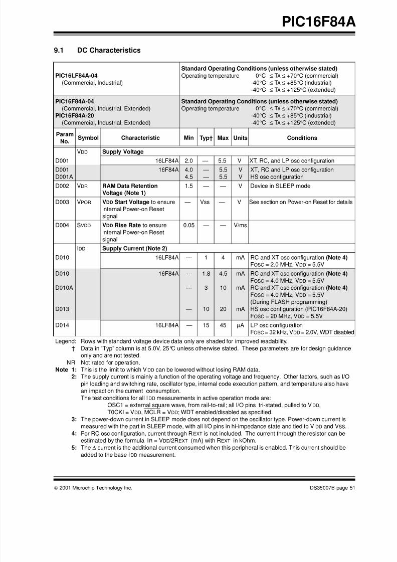
8/8/2019 Datasheet PIC16F84A
http://slidepdf.com/reader/full/datasheet-pic16f84a 53/88
2001 Microchip Technology Inc. DS35007B-page 51
PIC16F84A
9.1 DC Characteristics
PIC16LF84A-04
(Commercial, Industrial)
Standard Operating Conditions (unless otherwise stated)
Operating temperature 0°C ≤ TA ≤ +70°C (commercial)
-40°C ≤ TA ≤ +85°C (industrial)
-40°C ≤ TA ≤ +125°C (extended)
PIC16F84A-04
(Commercial, Industrial, Extended)
PIC16F84A-20
(Commercial, Industrial, Extended)
Standard Operating Conditions (unless otherwise stated)
Operating temperature 0°C ≤ TA ≤ +70°C (commercial)
-40°C ≤ TA ≤ +85°C (industrial)
-40°C ≤ TA ≤ +125°C (extended)
Param
No.Symbol Characteristic Min Typ† Max Units Conditions
VDD Supply Voltage
D001 16LF84A 2.0 — 5.5 V XT, RC, and LP osc configuration
D001
D001A
16F84A 4.0
4.5
—
—
5.5
5.5
V
V
XT, RC and LP osc configuration
HS osc configuration
D002 VDR RAM Data Retention
Voltage (Note 1)
1.5 — — V Device in SLEEP mode
D003 VPOR VDD Start Voltage to ensure
internal Power-on Reset
signal
— Vss — V See section on Power-on Reset for details
D004 SVDD VDD Rise Rate to ensure
internal Power-on Reset
signal
0.05 — — V/ms
IDD Supply Current (Note 2)
D010 16LF84A — 1 4 mA RC and XT osc configuration (Note 4)
FOSC = 2.0 MHz, VDD = 5.5V
D010
D010A
D013
16F84A —
—
—
1.8
3
10
4.5
10
20
mA
mA
mA
RC and XT osc configuration (Note 4)
FOSC = 4.0 MHz, VDD = 5.5V
RC and XT osc configuration (Note 4)
FOSC = 4.0 MHz, VDD = 5.5V(During FLASH programming)
HS osc configuration (PIC16F84A-20)
FOSC = 20 MHz, VDD = 5.5V
D014 16LF84A — 15 45 µA LP osc configuration
FOSC = 32 kHz, VDD = 2.0V, WDT disabled
Legend: Rows with standard voltage device data only are shaded for improved readability.
† Data in "Typ" column is at 5.0V, 25°C unless otherwise stated. These parameters are for design guidance
only and are not tested.
NR Not rated for operation.
Note 1: This is the limit to which VDD can be lowered without losing RAM data.
2: The supply current is mainly a function of the operating voltage and frequency. Other factors, such as I/O
pin loading and switching rate, oscillator type, internal code execution pattern, and temperature also have
an impact on the current consumption.The test conditions for all IDD measurements in active operation mode are:
OSC1 = external square wave, from rail-to-rail; all I/O pins tri-stated, pulled to VDD,
T0CKI = VDD, MCLR = VDD; WDT enabled/disabled as specified.
3: The power-down current in SLEEP mode does not depend on the oscillator type. Power-down current is
measured with the part in SLEEP mode, with all I/O pins in hi-impedance state and tied to VDD and VSS.
4: For RC osc configuration, current through REXT is not included. The current through the resistor can be
estimated by the formula IR = VDD /2REXT (mA) with REXT in kOhm.
5: The ∆ current is the additional current consumed when this peripheral is enabled. This current should be
added to the base IDD measurement.

8/8/2019 Datasheet PIC16F84A
http://slidepdf.com/reader/full/datasheet-pic16f84a 54/88
PIC16F84A
DS35007B-page 52 2001 Microchip Technology Inc.
IPD Power-down Current (Note 3)
D020 16LF84A
D020 16F84A-20
16F84A-04
D021A 16LF84A — 0.4 1.0 µA VDD = 2.0V, WDT disabled, industrial
D021A 16F84A-2016F84A-04
— —
1.51.0
3.53.0
µAµA
VDD = 4.5V, WDT disabled, industrialVDD = 4.0V, WDT disabled, industrial
D021B 16F84A-20
16F84A-04
—
—
1.5
1.0
5.5
5.0
µA
µA
VDD = 4.5V, WDT disabled, extended
VDD = 4.0V, WDT disabled, extended
D022 ∆IWDT
Module Differential Current
(Note 5)
Watchdog Timer —
—
—
—
—
.20
3.5
3.5
4.8
4.8
16
20
28
25
30
µA
µA
µA
µA
µA
VDD = 2.0V, Industrial, Commercial
VDD = 4.0V, Commercial
VDD = 4.0V, Industrial, Extended
VDD = 4.5V, Commercial
VDD = 4.5V, Industrial, Extended
9.1 DC Characteristics (Continued)
PIC16LF84A-04
(Commercial, Industrial)
Standard Operating Conditions (unless otherwise stated)
Operating temperature 0°C ≤ TA ≤ +70°C (commercial)
-40°C ≤ TA ≤ +85°C (industrial)
-40°C ≤ TA ≤ +125°C (extended)
PIC16F84A-04
(Commercial, Industrial, Extended)
PIC16F84A-20
(Commercial, Industrial, Extended)
Standard Operating Conditions (unless otherwise stated)
Operating temperature 0°C ≤ TA ≤ +70°C (commercial)
-40°C ≤ TA ≤ +85°C (industrial)
-40°C ≤ TA ≤ +125°C (extended)
Param
No.Symbol Characteristic Min Typ† Max Units Conditions
Legend: Rows with standard voltage device data only are shaded for improved readability.
† Data in "Typ" column is at 5.0V, 25°C unless otherwise stated. These parameters are for design guidance
only and are not tested.NR Not rated for operation.
Note 1: This is the limit to which VDD can be lowered without losing RAM data.
2: The supply current is mainly a function of the operating voltage and frequency. Other factors, such as I/O
pin loading and switching rate, oscillator type, internal code execution pattern, and temperature also have
an impact on the current consumption.
The test conditions for all IDD measurements in active operation mode are:
OSC1 = external square wave, from rail-to-rail; all I/O pins tri-stated, pulled to VDD,
T0CKI = VDD, MCLR = VDD; WDT enabled/disabled as specified.
3: The power-down current in SLEEP mode does not depend on the oscillator type. Power-down current is
measured with the part in SLEEP mode, with all I/O pins in hi-impedance state and tied to VDD and VSS.
4: For RC osc configuration, current through REXT is not included. The current through the resistor can be
estimated by the formula IR = VDD /2REXT (mA) with REXT in kOhm.
5: The ∆ current is the additional current consumed when this peripheral is enabled. This current should be
added to the base IDD measurement.

8/8/2019 Datasheet PIC16F84A
http://slidepdf.com/reader/full/datasheet-pic16f84a 55/88
2001 Microchip Technology Inc. DS35007B-page 53
PIC16F84A
9.2 DC Characteristics: PIC16F84A-04 (Commercial, Industrial)PIC16F84A-20 (Commercial, Industrial)PIC16LF84A-04 (Commercial, Industrial)
DC CharacteristicsAll Pins Except Power Supply Pins
Standard Operating Conditions (unless otherwise stated)
Operating temperature 0°C ≤ TA ≤ +70°C (commercial)
-40°C ≤ TA ≤ +85°C (industrial)
Operating voltage VDD range as described in DC specifications
(Section 9.1)
Param
No.Symbol Characteristic Min Typ† Max Units Conditions
VIL Input Low Voltage
I/O ports:
D030 with TTL buffer VSS — 0.8 V 4.5V ≤ VDD ≤ 5.5V (Note 4)
D030A VSS — 0.16VDD V Entire range (Note 4)
D031 with Schmitt Trigger buffer VSS — 0.2VDD V Entire range
D032 MCLR, RA4/T0CKI VSS — 0.2VDD V
D033 OSC1 (XT, HS and LP modes) VSS — 0.3VDD V (Note 1)
D034 OSC1 (RC mode) VSS — 0.1VDD V
VIH Input High Voltage
I/O ports: —
D040
D040A
with TTL buffer 2.0
0.25VDD+0.8
—
—
VDD
VDD
V
V
4.5V ≤ VDD ≤ 5.5V (Note 4)
Entire range (Note 4)
D041 with Schmitt Trigger buffer 0.8 VDD — VDD Entire range
D042 MCLR, 0.8 VDD — VDD V
D042A RA4/T0CKI 0.8 VDD — 8.5 V
D043 OSC1 (XT, HS and LP modes) 0.8 VDD — VDD V (Note 1)
D043A OSC1 (RC mode) 0.9 VDD VDD V
D050 VHYS Hysteresis of Schmitt TriggerInputs
— 0.1 — V
D070 IPURB PORTB Weak Pull-up Current 50 250 400 µA VDD = 5.0V, VPIN = VSS
IIL Input Leakage Current
(Notes 2, 3)
D060 I/O ports — — ±1 µA Vss ≤ VPIN ≤ VDD,
Pin at hi-impedance
D061 MCLR, RA4/T0CKI — — ±5 µA Vss ≤ VPIN ≤ VDD
D063 OSC1 — — ±5 µA Vss ≤ VPIN ≤ VDD, XT, HS
and LP osc configuration
† Data in “Typ” column is at 5.0V, 25°C unless otherwise stated. These parameters are for design guidance
only and are not tested.
Note 1: In RC oscillator configuration, the OSC1 pin is a Schmitt Trigger input. Do not drive the PIC16F84A with anexternal clock while the device is in RC mode, or chip damage may result.
2: The leakage current on the MCLR pin is strongly dependent on the applied voltage level. The specified
levels represent normal operating conditions. Higher leakage current may be measured at different input
voltages.
3: Negative current is defined as coming out of the pin.
4: The user may choose the better of the two specs.

8/8/2019 Datasheet PIC16F84A
http://slidepdf.com/reader/full/datasheet-pic16f84a 56/88
PIC16F84A
DS35007B-page 54 2001 Microchip Technology Inc.
VOL Output Low Voltage
D080 I/O ports — — 0.6 V IOL = 8.5 mA, VDD = 4.5V
D083 OSC2/CLKOUT — — 0.6 V IOL = 1.6 mA, VDD = 4.5V,
(RC mode only)
VOH Output High Voltage
D090 I/O ports (Note 3) VDD-0.7 — — V IOH = -3.0 mA, VDD = 4.5V
D092 OSC2/CLKOUT (Note 3) VDD-0.7 — — V IOH = -1.3 mA, VDD = 4.5V(RC mode only)
VOD Open Drain High Voltage
D150 RA4 pin — — 8.5 V
Capacitive Loading Specs on
Output Pins
D100 COSC2 OSC2 pin — — 15 pF In XT, HS and LP modes
when external clock is used
to drive OSC1
D101 CIO All I/O pins and OSC2
(RC mode)
— — 50 pF
Data EEPROM Memory
D120 ED Endurance 1M 10M — E/W 25°C at 5VD121 VDRW VDD for read/write VMIN — 5.5 V VMIN = Minimum operating
voltage
D122 TDEW Erase/Write cycle time — 4 8 ms
Program FLASH Memory
D130 EP Endurance 1000 10K — E/W
D131 VPR VDD for read VMIN — 5.5 V VMIN = Minimum operating
voltage
D132 VPEW VDD for erase/write 4.5 — 5.5 V
D133 TPEW Erase/Write cycle time — 4 8 ms
9.2 DC Characteristics: PIC16F84A-04 (Commercial, Industrial)PIC16F84A-20 (Commercial, Industrial)PIC16LF84A-04 (Commercial, Industrial) (Continued)
DC CharacteristicsAll Pins Except Power Supply Pins
Standard Operating Conditions (unless otherwise stated)
Operating temperature 0°C ≤ TA ≤ +70°C (commercial)
-40°C ≤ TA ≤ +85°C (industrial)Operating voltage VDD range as described in DC specifications
(Section 9.1)
Param
No.Symbol Characteristic Min Typ† Max Units Conditions
† Data in “Typ” column is at 5.0V, 25°C unless otherwise stated. These parameters are for design guidance
only and are not tested.
Note 1: In RC oscillator configuration, the OSC1 pin is a Schmitt Trigger input. Do not drive the PIC16F84A with anexternal clock while the device is in RC mode, or chip damage may result.
2: The leakage current on the MCLR pin is strongly dependent on the applied voltage level. The specified
levels represent normal operating conditions. Higher leakage current may be measured at different input
voltages.
3: Negative current is defined as coming out of the pin.
4: The user may choose the better of the two specs.
8/8/2019 Datasheet PIC16F84A
http://slidepdf.com/reader/full/datasheet-pic16f84a 57/88
2001 Microchip Technology Inc. DS35007B-page 55
PIC16F84A
9.3 AC (Timing) Characteristics
9.3.1 TIMING PARAMETER SYMBOLOGY
The timing parameter symbols have been created fol-
lowing one of the following formats:
1. TppS2ppS2. TppS
T
F Frequency T Time
Lowercase letters (pp) and their meanings:
pp
2 to os, osc OSC1
ck CLKOUT ost oscillator start-up timer
cy cycle time pwrt power-up timer
io I/O port rbt RBx pins
inp INT pin t0 T0CKI
mp MCLR wdt watchdog timer
Uppercase letters and their meanings:
S
F Fall P Period
H High R Rise
I Invalid (high impedance) V Valid
L Low Z High Impedance

8/8/2019 Datasheet PIC16F84A
http://slidepdf.com/reader/full/datasheet-pic16f84a 58/88
PIC16F84A
DS35007B-page 56 2001 Microchip Technology Inc.
9.3.2 TIMING CONDITIONS
The temperature and voltages specified in Table 9-1
apply to all timing specifications unless otherwise
noted. All timings are measured between high and low
measurement points as indicated in Figure 9-4.
Figure 9-5 specifies the load conditions for the timing
specifications.
TABLE 9-1: TEMPERATURE AND VOLTAGE SPECIFICATIONS - AC
FIGURE 9-4: PARAMETER MEASUREMENT INFORMATION
FIGURE 9-5: LOAD CONDITIONS
AC CHARACTERISTICS
Standard Operating Conditions (unless otherwise stated)
Operating temperature 0°C ≤ TA ≤ +70°C for commercial
-40°C ≤ TA ≤ +85°C for industrial
Operating voltage VDD range as described in DC specifications (Section 9.1)
0.9 VDD (High)
0.1 VDD (Low)
0.8 VDD RC
0.3 VDD XTAL
OSC1 Measurement Points I/O Port Measurement Points
0.15 VDD RC
0.7 VDD XTAL(High)
(Low)
Load Condition 1 Load Condition 2
Pin
RL
CL
VSS
VDD /2
VSS
CLPin
RL = 464Ω
CL = 50 pF for all pins except OSC2
15 pF for OSC2 output

8/8/2019 Datasheet PIC16F84A
http://slidepdf.com/reader/full/datasheet-pic16f84a 59/88
2001 Microchip Technology Inc. DS35007B-page 57
PIC16F84A
9.3.3 TIMING DIAGRAMS AND SPECIFICATIONS
FIGURE 9-6: EXTERNAL CLOCK TIMING
OSC1
CLKOUT
Q4 Q1 Q2 Q3 Q4 Q1
1 3 3 4 4
2
TABLE 9-2: EXTERNAL CLOCK TIMING REQUIREMENTS
Param No. Sym Characteristic Min Typ† Max Units Conditions
FOSC External CLKIN Frequency(1) DC — 2 MHz XT, RC osc (-04, LF)
DC — 4 MHz XT, RC osc (-04)
DC — 20 MHz HS osc (-20)
DC — 200 kHz LP osc (-04, LF)
Oscillator Frequency(1) DC — 2 MHz RC osc (-04, LF)
DC — 4 MHz RC osc (-04)
0.1 — 2 MHz XT osc (-04, LF)
0.1 — 4 MHz XT osc (-04)
1.0 — 20 MHz HS osc (-20)
DC — 200 kHz LP osc (-04, LF)
1 TOSC External CLKIN Period(1) 500 — — ns XT, RC osc (-04, LF)
250 — — ns XT, RC osc (-04)
50 — — ns HS osc (-20)
5.0 — — µs LP osc (-04, LF)
Oscillator Period
(1)
500 — — ns RC osc (-04, LF)250 — — ns RC osc (-04)
500 — 10,000 ns XT osc (-04, LF)
250 — 10,000 ns XT osc (-04)
50 — 1,000 ns HS osc (-20)
5.0 — — µs LP osc (-04, LF)
2 TCY Instruction Cycle Time(1) 0.2 4/FOSC DC µs
3 TosL,
TosH
Clock in (OSC1) High or Low
Time
60 — — ns XT osc (-04, LF)
50 — — ns XT osc (-04)
2.0 — — µs LP osc (-04, LF)
17.5 — — ns HS osc (-20)
4 TosR,
TosF
Clock in (OSC1) Rise or Fall
Time
25 — — ns XT osc (-04)
50 — — ns LP osc (-04, LF)7.5 — — ns HS osc (-20)
† Data in "Typ" column is at 5.0V, 25°C unless otherwise stated. These parameters are for design guidance
only and are not tested.
Note 1: Instruction cycle period (TCY) equals four times the input oscillator time-base period. All specified values
are based on characterization data for that particular oscillator type under standard operating conditions
with the device executing code. Exceeding these specified limits may result in an unstable oscillator opera-
tion and/or higher than expected current consumption. All devices are tested to operate at "Min." values
with an external clock applied to the OSC1 pin.
When an external clock input is used, the "Max." cycle time limit is "DC" (no clock) for all devices.
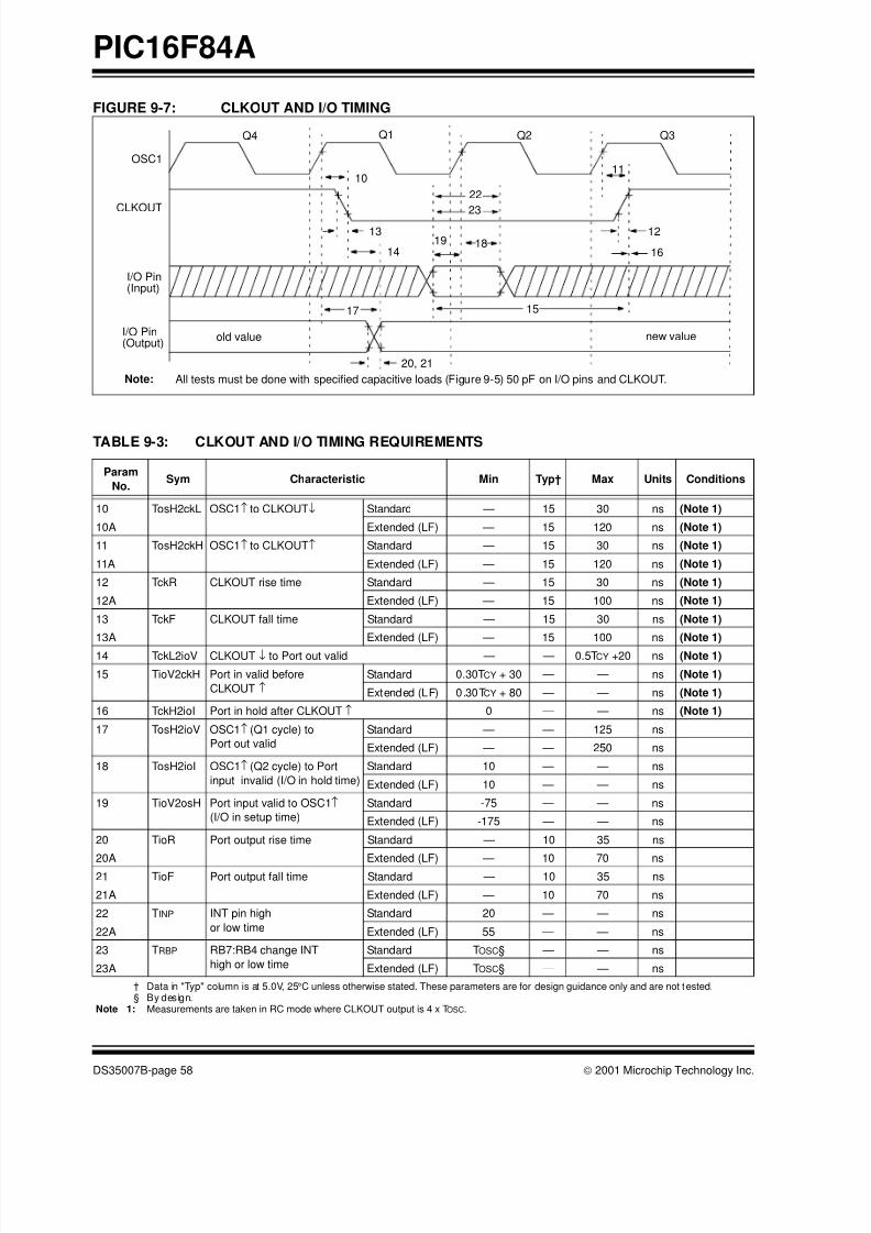
8/8/2019 Datasheet PIC16F84A
http://slidepdf.com/reader/full/datasheet-pic16f84a 60/88
PIC16F84A
DS35007B-page 58 2001 Microchip Technology Inc.
FIGURE 9-7: CLKOUT AND I/O TIMING
TABLE 9-3: CLKOUT AND I/O TIMING REQUIREMENTS
OSC1
CLKOUT
I/O Pin(Input)
I/O Pin(Output)
Q4 Q1 Q2 Q3
10
13
14
17
20, 21
22
23
19 18
15
11
12
16
old value new value
Note: All tests must be done with specified capacitive loads (Figure 9-5) 50 pF on I/O pins and CLKOUT.
Param
No.Sym Characteristic Min Typ† Max Units Conditions
10 TosH2ckL OSC1↑ to CLKOUT↓ Standard — 15 30 ns (Note 1)
10A Extended (LF) — 15 120 ns (Note 1)
11 TosH2ckH OSC1↑ to CLKOUT↑ Standard — 15 30 ns (Note 1)
11A Extended (LF) — 15 120 ns (Note 1)
12 TckR CLKOUT rise time Standard — 15 30 ns (Note 1)
12A Extended (LF) — 15 100 ns (Note 1)
13 TckF CLKOUT fall time Standard — 15 30 ns (Note 1)
13A Extended (LF) — 15 100 ns (Note 1)
14 TckL2ioV CLKOUT ↓ to Port out valid — — 0.5TCY +20 ns (Note 1)
15 TioV2ckH Port in valid before
CLKOUT ↑
Standard 0.30TCY + 30 — — ns (Note 1)
Extended (LF) 0.30TCY + 80 — — ns (Note 1)
16 TckH2ioI Port in hold after CLKOUT ↑ 0 — — ns (Note 1)
17 TosH2ioV OSC1↑ (Q1 cycle) to
Port out valid
Standard — — 125 ns
Extended (LF) — — 250 ns
18 TosH2ioI OSC1↑ (Q2 cycle) to Port
input invalid (I/O in hold time)
Standard 10 — — ns
Extended (LF) 10 — — ns
19 TioV2osH Port input valid to OSC1↑(I/O in setup time)
Standard -75 — — ns
Extended (LF) -175 — — ns
20 TioR Port output rise time Standard — 10 35 ns
20A Extended (LF) — 10 70 ns21 TioF Port output fall time Standard — 10 35 ns
21A Extended (LF) — 10 70 ns
22 TINP INT pin high
or low time
Standard 20 — — ns
22A Extended (LF) 55 — — ns
23 TRBP RB7:RB4 change INT
high or low time
Standard TOSC§ — — ns
23A Extended (LF) TOSC§ — — ns
† Data in "Typ" column is at 5.0V, 25°C unless otherwise stated. These parameters are for design guidance only and are not tested.§ By design.
Note 1: Measurements are taken in RC mode where CLKOUT output is 4 x TOSC.

8/8/2019 Datasheet PIC16F84A
http://slidepdf.com/reader/full/datasheet-pic16f84a 61/88
2001 Microchip Technology Inc. DS35007B-page 59
PIC16F84A
FIGURE 9-8: RESET, WATCHDOG TIMER, OSCILLATOR START-UP TIMER AND POWER-UPTIMER TIMING
TABLE 9-4: RESET, WATCHDOG TIMER, OSCILLATOR START-UP TIMER ANDPOWER-UP TIMER REQUIREMENTS
VDD
MCLR
InternalPOR
PWRTTime-out
OSCTime-out
InternalReset
WatchdogTimerReset
33
32
30
3134
I/O Pins
34
ParameterNo. Sym Characteristic Min Typ† Max Units Conditions
30 TmcL MCLR Pulse Width (low) 2 — — µs VDD = 5.0V
31 TWDTWatchdog Timer Time-out
Period (No Prescaler)7 18 33 ms VDD = 5.0V
32 TOSTOscillation Start-up Timer
Period1024TOSC ms TOSC = OSC1 period
33 TPWRT Power-up Timer Period 28 72 132 ms VDD = 5.0V
34 TIOZ I/O hi-impedance from MCLR
Low or RESET — — 100 ns
† Data in "Typ" column is at 5V, 25°C, unless otherwise stated. These parameters are for design guidance
only and are not tested.

8/8/2019 Datasheet PIC16F84A
http://slidepdf.com/reader/full/datasheet-pic16f84a 62/88
PIC16F84A
DS35007B-page 60 2001 Microchip Technology Inc.
FIGURE 9-9: TIMER0 CLOCK TIMINGS
TABLE 9-5: TIMER0 CLOCK REQUIREMENTS
RA4/T0CKI
40 41
42
Parameter
No.Sym Characteristic Min Typ† Max Units Conditions
40 Tt0H T0CKI High Pulse
Width
No Prescaler 0.5TCY + 20 — — ns
With Prescaler 5030
— —
— —
nsns
2.0V ≤ VDD ≤ 3.0V3.0V ≤ VDD ≤ 6.0V
41 Tt0L T0CKI Low Pulse
Width
No Prescaler 0.5TCY + 20 — — ns
With Prescaler 50
20
—
—
—
—
ns
ns
2.0V ≤ VDD ≤ 3.0V
3.0V ≤ VDD ≤ 6.0V
42 Tt0P T0CKI Period TCY + 40
N
— — ns N = prescale value
(2, 4, ..., 256)
† Data in "Typ" column is at 5.0V, 25°C, unless otherwise stated. These parameters are for design guidance
only and are not tested.

8/8/2019 Datasheet PIC16F84A
http://slidepdf.com/reader/full/datasheet-pic16f84a 63/88
2001 Microchip Technology Inc. DS35007B-page 61
PIC16F84A
10.0 DC/AC CHARACTERISTIC GRAPHS
The graphs provided in this section are for design guidance and are not tested.
In some graphs, the data presented are outside specified operating range (i.e., outside specified VDD range). This is
for information only and devices are ensured to operate properly only within the specified range.
The data presented in this section is a statistical summary of data collected on units from different lots over a period
of time and matrix samples. ‘Typical’ represents the mean of the distribution at 25°C. ‘Max’ or ‘Min’ represents(mean + 3σ) or (mean - 3σ), respectively, where σ is a standard deviation over the whole temperature range.

8/8/2019 Datasheet PIC16F84A
http://slidepdf.com/reader/full/datasheet-pic16f84a 64/88
PIC16F84A
DS35007B-page 62 © 2001 Microchip Technology Inc.
FIGURE 10-1: TYPICAL IDD vs. FOSC OVER VDD (HS MODE, 25°C)
FIGURE 10-2: MAXIMUM IDD vs. FOSC OVER VDD (HS MODE, -40° TO +125°C)
0.0
0.5
1.0
1.5
2.0
2.5
3.0
3.5
4.0
4 6 8 10 12 14 16 18 20FOSC (MHz)
I D D ( m A )
2.5 V
3.0 V
3.5 V
4.0 V
4.5 V
5.0 V
5.5 V
2.0 V
0.0
0.5
1.0
1.5
2.0
2.5
3.0
3.5
4.0
4.5
5.0
4 6 8 10 12 14 16 18 20
FOSC (MHz)
I D D ( m A )
2.5 V
3.0 V
3.5 V
4.0 V
4.5 V
5.0 V
5.5 V
2.0 V
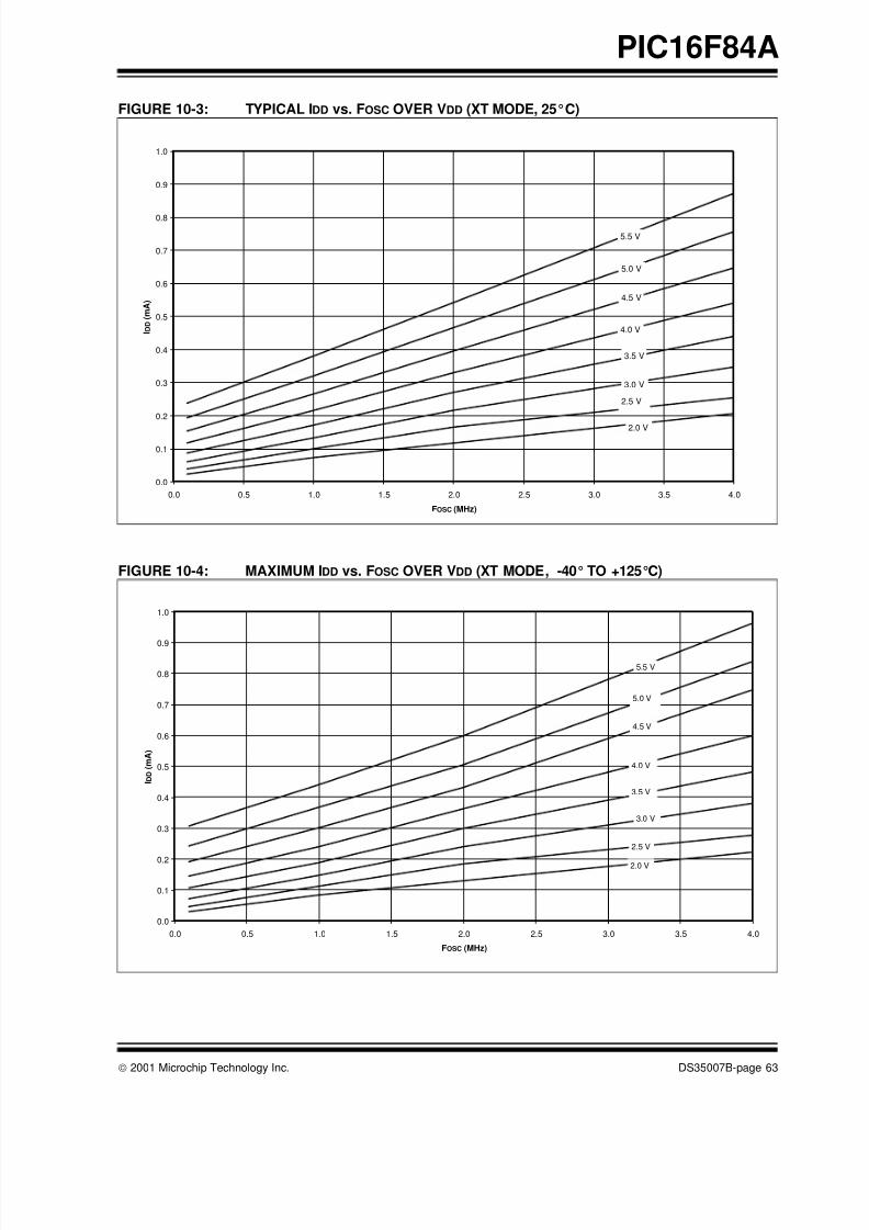
8/8/2019 Datasheet PIC16F84A
http://slidepdf.com/reader/full/datasheet-pic16f84a 65/88
2001 Microchip Technology Inc. DS35007B-page 63
PIC16F84A
FIGURE 10-3: TYPICAL IDD vs. FOSC OVER VDD (XT MODE, 25°C)
FIGURE 10-4: MAXIMUM IDD vs. FOSC OVER VDD (XT MODE, -40° TO +125°C)
0.0
0.1
0.2
0.3
0.4
0.5
0.6
0.7
0.8
0.9
1.0
0.0 0.5 1.0 1.5 2.0 2.5 3.0 3.5 4.0
FOSC (MHz)
I D D ( m A )
2.0 V
2.5 V
3.0 V
3.5 V
4.0 V
4.5 V
5.0 V
5.5 V
0.0
0.1
0.2
0.3
0.4
0.5
0.6
0.7
0.8
0.9
1.0
0.0 0.5 1.0 1.5 2.0 2.5 3.0 3.5 4.0
FOSC (MHz)
I D D ( m A )
2.0 V
2.5 V
3.0 V
3.5 V
4.0 V
4.5 V
5.0 V
5.5 V

8/8/2019 Datasheet PIC16F84A
http://slidepdf.com/reader/full/datasheet-pic16f84a 66/88
PIC16F84A
DS35007B-page 64 © 2001 Microchip Technology Inc.
FIGURE 10-5: TYPICAL IDD vs. FOSC OVER VDD (LP MODE, 25°C)
FIGURE 10-6: MAXIMUM IDD vs. FOSC OVER VDD (LP MODE, -40° TO +125°C)
0
10
20
30
40
50
60
70
80
25 50 75 100 125 150 175 200
FOSC (kHz)
I D D ( µ A )
5.0 V
5.5 V
4.0 V
3.5 V
4.5 V
3.0 V
2.5 V
2.0 V
0
50
100
150
200
250
25 50 75 100 125 150 175 200
FOSC (kHz)
I D D ( µ A )
5.0 V
5.5 V
4.0 V
3.5 V
4.5 V
3.0 V
2.5 V
2.0 V

8/8/2019 Datasheet PIC16F84A
http://slidepdf.com/reader/full/datasheet-pic16f84a 67/88
2001 Microchip Technology Inc. DS35007B-page 65
PIC16F84A
FIGURE 10-7: AVERAGE FOSC vs. VDD FOR R (RC MODE, C = 22 pF, 25°C)
FIGURE 10-8: AVERAGE FOSC vs. VDD FOR R (RC MODE, C = 100 pF, 25°C)
0.0
2.0
4.0
6.0
8.0
10.0
12.0
14.0
16.0
2.0 2.5 3.0 3.5 4.0 4.5 5.0 5.5VDD (V)
F r e q ( M H z )
5.1 kΩ
3.3 kΩ
10 kΩ
100 kΩ
0
200
400
600
800
1000
1200
1400
1600
1800
2000
2.0 2.5 3.0 3.5 4.0 4.5 5.0 5.5
VDD (V)
F r e q ( K H z )
100 kΩ
10 kΩ
5.1 kΩ
3.3 kΩ

8/8/2019 Datasheet PIC16F84A
http://slidepdf.com/reader/full/datasheet-pic16f84a 68/88
PIC16F84A
DS35007B-page 66 © 2001 Microchip Technology Inc.
FIGURE 10-9: AVERAGE FOSC vs. VDD FOR R (RC MODE, C = 300 pF, 25°C)
FIGURE 10-10: IPD vs. VDD (SLEEP MODE, ALL PERIPHERALS DISABLED)
0
100
200
300
400
500
600
700
800
900
2.0 2.5 3.0 3.5 4.0 4.5 5.0 5.5VDD (V)
F r e q ( K H z )
3.3 kΩ
5.1 kΩ
10 kΩ
100 kΩ
0.0
0.1
1.0
10.0
2.0 2.5 3.0 3.5 4.0 4.5 5.0 5.5
VDD (V)
I P D ( µ A )
Max
Typ
Typical: statist ical mean @ 25°CMaximum: mean + 3σ (-40°C to +125°C)Minimum: mean – 3σ (-40°C to +125°C)

8/8/2019 Datasheet PIC16F84A
http://slidepdf.com/reader/full/datasheet-pic16f84a 69/88
2001 Microchip Technology Inc. DS35007B-page 67
PIC16F84A
FIGURE 10-11: IPD vs. VDD (WDT MODE)
FIGURE 10-12: TYPICAL, MINIMUM, AND MAXIMUM WDT PERIOD vs. VDD OVER TEMP
0
1
2
3
4
5
6
7
8
9
10
11
12
13
14
15
2.0 2.5 3.0 3.5 4.0 4.5 5.0 5.5VDD (V)
I P D ( µ A )
Max
Typ
Typical: statist ical mean @ 25°CMaximum: mean + 3σ (-40°C to +125°C)Minimum: mean – 3σ (-40°C to +125°C)
0
10
20
30
40
50
60
2.0 2.5 3.0 3.5 4.0 4.5 5.0 5.5VDD (V)
W D T P e r i o d ( m s )
Max
Min
Typ
Typical: statistical mean @ 25°CMaximum: mean + 3σ (-40°C to +125°C)Minimum: mean – 3σ (-40°C to +125°C)
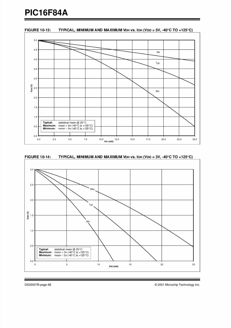
8/8/2019 Datasheet PIC16F84A
http://slidepdf.com/reader/full/datasheet-pic16f84a 70/88

8/8/2019 Datasheet PIC16F84A
http://slidepdf.com/reader/full/datasheet-pic16f84a 71/88
2001 Microchip Technology Inc. DS35007B-page 69
PIC16F84A
FIGURE 10-15: TYPICAL, MINIMUM AND MAXIMUM VOL vs. IOL (VDD = 5V, -40°C TO +125°C)
FIGURE 10-16: TYPICAL, MINIMUM AND MAXIMUM VOL vs. IOL (VDD = 3V, -40°C TO +125°C)
0.0
0.1
0.2
0.3
0.4
0.5
0.6
0.7
0.8
0.9
1.0
0 5 10 15 20 25
IOL (mA)
V O L ( V )
Max
Typ
Min
Typical: statistical mean @ 25°CMaximum: mean + 3σ (-40°C to +125°C)Minimum: mean – 3σ (-40°C to +125°C)
0.0
0.2
0.4
0.6
0.8
1.0
1.2
1.4
1.6
1.8
0.0 2.5 5.0 7.5 10.0 12.5 15.0 17.5 20.0 22.5 25.0IOL (mA)
V O L ( V )
Max
Typ
Min
Typical: statistical mean @ 25°CMaximum: mean + 3σ (-40°C to +125°C)Minimum: mean – 3σ (-40°C to +125°C)
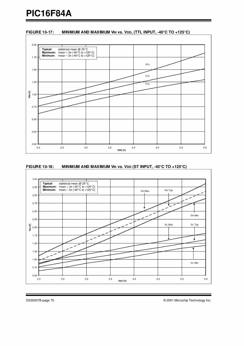
8/8/2019 Datasheet PIC16F84A
http://slidepdf.com/reader/full/datasheet-pic16f84a 72/88
PIC16F84A
DS35007B-page 70 © 2001 Microchip Technology Inc.
FIGURE 10-17: MINIMUM AND MAXIMUM VIN vs. VDD, (TTL INPUT, -40°C TO +125°C)
FIGURE 10-18: MINIMUM AND MAXIMUM VIN vs. VDD (ST INPUT, -40°C TO +125°C)
0.00
0.25
0.50
0.75
1.00
1.25
1.50
1.75
2.00
2.0 2.5 3.0 3.5 4.0 4.5 5.0 5.5VDD (V)
V I N ( V )
VTH
VTH
VTH
Typical: statist ical mean @ 25°CMaximum: mean + 3σ (-40°C to +125°C)Minimum: mean – 3σ (-40°C to +125°C)
0.50
0.75
1.00
1.25
1.50
1.75
2.00
2.25
2.50
2.75
3.00
3.25
3.50
2.0 2.5 3.0 3.5 4.0 4.5 5.0 5.5VDD (V)
V I N ( V )
VIH Max VIH Typ
VIH Min
VIL Max VIL Typ
VIL Min
Typical: statist ical mean @ 25°CMaximum: mean + 3σ (-40°C to +125°C)Minimum: mean – 3σ (-40°C to +125°C)

8/8/2019 Datasheet PIC16F84A
http://slidepdf.com/reader/full/datasheet-pic16f84a 73/88
2001 Microchip Technology Inc. DS35007B-page 71
PIC16F84A
11.0 PACKAGING INFORMATION
11.1 Package Marking Information
18-Lead PDIP
XXXXXXXXXXXXXXXXXXXXXXXXXXXXXXXXXX
YYWWNNN
YYWWNNNXXXXXXXXXXXX
XXXXXXXXXXXX
18-Lead SOIC
Example
XXXXXXXXXXXX
Example
YYWWNNNXXXXXXXXXXXXXXXXXXXXXX
20-Lead SSOP Example
Legend: XX...X Customer specific information*
Y Year code (last digit of calendar year)
YY Year code (last 2 digits of calendar year)
WW Week code (week of January 1 is week ‘01’)
NNN Alphanumeric traceability code
Note: In the event the full Microchip part number cannot be marked on one line, it will
be carried over to the next line thus limiting the number of available charactersfor customer specific information.
* Standard PICmicro device marking consists of Microchip part number, year code, week code, and
traceability code. For PICmicro device marking beyond this, certain price adders apply. Please check
with your Microchip sales office. For QTP devices, any special marking adders are included in QTP
price.
PIC16F84A-04I/P
0110017
0110017
/SOPIC16F84A-04
011001720/SSPIC16F84A-
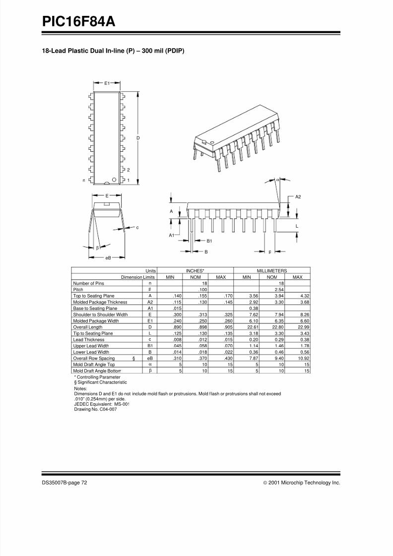
8/8/2019 Datasheet PIC16F84A
http://slidepdf.com/reader/full/datasheet-pic16f84a 74/88
PIC16F84A
DS35007B-page 72 2001 Microchip Technology Inc.
18-Lead Plastic Dual In-line (P) – 300 mil (PDIP)
1510515105βMold Draft Angle Bottom
1510515105αMold Draft Angle Top
10.929.407.87.430.370.310eBOverall Row Spacing §
0.560.460.36.022.018.014BLower Lead Width
1.781.461.14.070.058.045B1Upper Lead Width
0.380.290.20.015.012.008cLead Thickness
3.433.303.18.135.130.125LTip to Seating Plane
22.9922.8022.61.905.898.890DOverall Length
6.606.356.10.260.250.240E1Molded Package Width
8.267.947.62.325.313.300EShoulder to Shoulder Width
0.38.015A1Base to Seating Plane
3.683.302.92.145.130.115A2Molded Package Thickness
4.323.943.56.170.155.140ATop to Seating Plane
2.54.100pPitch
1818nNumber of Pins
MAXNOMMINMAXNOMMINDimension Limits
MILLIMETERSINCHES*Units
1
2
D
n
E1
c
eB
β
E
α
p
A2
L
B1
B
A
A1
* Controlling Parameter
Notes:Dimensions D and E1 do not include mold flash or protrusions. Mold f lash or protrusions shall not exceed.010” (0.254mm) per side.JEDEC Equivalent: MS-001Drawing No. C04-007
§ Significant Characteristic

8/8/2019 Datasheet PIC16F84A
http://slidepdf.com/reader/full/datasheet-pic16f84a 75/88
2001 Microchip Technology Inc. DS35007B-page 73
PIC16F84A
18-Lead Plastic Small Outline (SO) – Wide, 300 mil (SOIC)
Foot Angle φ 0 4 8 0 4 8
1512015120βMold Draft Angle Bottom
1512015120αMold Draft Angle Top
0.510.420.36.020.017.014BLead Width
0.300.270.23.012.011.009cLead Thickness
1.270.840.41.050.033.016LFoot Length
0.740.500.25.029.020.010hChamfer Distance
11.7311.5311.33.462.454.446DOverall Length
7.597.497.39.299.295.291E1Molded Package Width
10.6710.3410.01.420.407.394EOverall Width
0.300.200.10.012.008.004A1Standoff §
2.392.312.24.094.091.088A2Molded Package Thickness
2.642.502.36.104.099.093AOverall Height1.27.050
pPitch
1818nNumber of Pins
MAXNOMMINMAXNOMMINDimension Limits
MILLIMETERSINCHES*Units
Lβ
c
φ
h
45°
1
2
D
p
nB
E1
E
α
A2
A1
A
* Controlling Parameter
Notes:Dimensions D and E1 do not include mold flash or protrusions. Mold flash or protrusions shall not exceed.010” (0.254mm) per side.JEDEC Equivalent: MS-013Drawing No. C04-051
§ Significant Characteristic

8/8/2019 Datasheet PIC16F84A
http://slidepdf.com/reader/full/datasheet-pic16f84a 76/88
PIC16F84A
DS35007B-page 74 2001 Microchip Technology Inc.
20-Lead Plastic Shrink Small Outline (SS) – 209 mil, 5.30 mm (SSOP)
10501050βMold Draft Angle Bottom
10501050αMold Draft Angle Top
0.380.320.25.015.013.010BLead Width
203.20101.600.00840φFoot Angle
0.250.180.10.010.007.004cLead Thickness
0.940.750.56.037.030.022LFoot Length
7.347.207.06.289.284.278DOverall Length
5.385.255.11.212.207.201E1Molded Package Width
8.187.857.59.322.309.299EOverall Width
0.250.150.05.010.006.002A1Standoff §
1.831.731.63.072.068.064A2Molded Package Thickness1.981.851.73.078.073.068AOverall Height
0.65.026pPitch
2020nNumber of Pins
MAXNOMMINMAXNOMMINDimension Limits
MILLIMETERSINCHES*Units
2
1
D
p
n
B
E
E1
L
c
β
φ
α
A2A
A1
* Controlling Parameter
Notes:Dimensions D and E1 do not include mold flash or protrusions. Mold flash or protrusions shall not exceed
.010” (0.254mm) per side.JEDEC Equivalent: MO-150Drawing No. C04-072
§ Significant Characteristic

8/8/2019 Datasheet PIC16F84A
http://slidepdf.com/reader/full/datasheet-pic16f84a 77/88
2001 Microchip Technology Inc. DS35007B-page 75
PIC16F84A
APPENDIX A: REVISION HISTORY
Version Date Revision Description
A 9/98 This is a new data sheet. However, the devices described in this data sheet are
the upgrades to the devices found in the PIC16F8X Data Sheet , DS30430.
B 8/01 Added DC and AC Characteristics Graphs and Tables to Section 10.

8/8/2019 Datasheet PIC16F84A
http://slidepdf.com/reader/full/datasheet-pic16f84a 78/88
PIC16F84A
DS35007B-page 76 2001 Microchip Technology Inc.
APPENDIX B: CONVERSION CONSIDERATIONS
Considerations for converting from one PIC16X8X
device to another are listed in Table 1.
TABLE 1: CONVERSION CONSIDERATIONS - PIC16C84, PIC16F83/F84, PIC16CR83/CR84,PIC16F84A
Difference PIC16C84 PIC16F83/F84PIC16CR83/
CR84PIC16F84A
Program Memory Size 1K x 14 512 x 14 / 1K x 14 512 x 14 / 1K x 14 1K x 14
Data Memory Size 36 x 8 36 x 8 / 68 x 8 36 x 8 / 68 x 8 68 x 8
Voltage Range 2.0V - 6.0V
(-40°C to +85°C)
2.0V - 6.0V
(-40°C to +85°C)
2.0V - 6.0V
(-40°C to +85°C)
2.0V - 5.5V
(-40°C to +125°C)
Maximum Operating Fre-
quency
10 MHz 10 MHz 10 MHz 20 MHz
Supply Current (IDD).
See parameter # D014 in
the electrical specs for
more detail.
IDD (typ) = 60 µA
IDD (max) = 400 µA
(LP osc, FOSC = 32 kHz,
VDD = 2.0V,
WDT disabled)
IDD (typ) = 15 µA
IDD (max) = 45 µA
(LP osc, FOSC = 32 kHz,
VDD = 2.0V,
WDT disabled)
IDD (typ) = 15 µA
IDD (max) = 45 µA
(LP osc, FOSC = 32 kHz,
VDD = 2.0V,
WDT disabled)
IDD (typ) = 15 µA
IDD (max) = 45 µA
(LP osc, FOSC = 32 kHz,
VDD = 2.0V,
WDT disabled)
Power-down Current
(IPD). See parameters #
D020, D021, and D021A
in the electrical specs for
more detail.
IPD (typ) = 26 µA
IPD (max) = 100 µA
(VDD = 2.0V,
WDT disabled, industrial)
IPD (typ) = 0.4 µA
IPD (max) = 9 µA
(VDD = 2.0V,
WDT disabled, industrial)
IPD (typ) = 0.4 µA
IPD (max) = 6 µA
(VDD = 2.0V,
WDT disabled, industrial)
IPD (typ) = 0.4 µA
IPD (max) = 1 µA
(VDD = 2.0V,
WDT disabled, industrial)
Input Low Voltage (VIL).
See parameters # D032
and D034 in the electrical
specs for more detail.
VIL (max) = 0.2VDD
(OSC1, RC mode)
VIL (max) = 0.1VDD
(OSC1, RC mode)
VIL (max) = 0.1VDD
(OSC1, RC mode)
VIL (max) = 0.1VDD
(OSC1, RC mode)
Input High Voltage (VIH).
See parameter # D040 in
the electrical specs for
more detail.
VIH (min) = 0.36VDD
(I/O Ports with TTL,
4.5V ≤ VDD ≤ 5.5V)
VIH (min) = 2.4V
(I/O Ports with TTL,
4.5V ≤ VDD ≤ 5.5V)
VIH (min) = 2.4V
(I/O Ports with TTL,
4.5V ≤ VDD ≤ 5.5V)
VIH (min) = 2.4V
(I/O Ports with TTL,
4.5V ≤ VDD ≤ 5.5V)
Data EEPROM Memory
Erase/Write cycle time
(TDEW). See parameter #
D122 in the electrical
specs for more detail.
TDEW (typ) = 10 ms
TDEW (max) = 20 ms
TDEW (typ) = 10 ms
TDEW (max) = 20 ms
TDEW (typ) = 10 ms
TDEW (max) = 20 ms
TDEW (typ) = 4 ms
TDEW (max) = 8 ms
Port Output Rise/Fall
time (TioR, TioF). See
parameters #20, 20A,
21, and 21A in the elec-
trical specs for more
detail.
TioR, TioF (max) = 25 ns
(C84)
TioR, TioF (max) = 60 ns
(LC84)
TioR, TioF (max) = 35 ns
(C84)
TioR, TioF (max) = 70 ns
(LC84)
TioR, TioF (max) = 35 ns
(C84)
TioR, TioF (max) = 70 ns
(LC84)
TioR, TioF (max) = 35 ns
(C84)
TioR, TioF (max) = 70 ns
(LC84)
MCLR on-chip filter. See
parameter #30 in the
electrical specs for moredetail.
No Yes Yes Yes
PORTA and crystal oscil-
lator values less than
500 kHz
For crystal oscillator con-
figurations operating
below 500 kHz, the device
may generate a spurious
internal Q-clock when
PORTA<0> switches
state.
N/A N/A N/A
RB0/INT pin TTL TTL/ST*
(*Schmitt Trigger)
TTL/ST*
(*Schmitt Trigger)
TTL/ST*
(*Schmitt Trigger)

8/8/2019 Datasheet PIC16F84A
http://slidepdf.com/reader/full/datasheet-pic16f84a 79/88
2001 Microchip Technology Inc. DS35007B-page 77
PIC16F84A
EEADR<7:6> and IDD It is recommended that
the EEADR<7:6> bits becleared. When either of
these bits is set, the maxi-
mum IDD for the device is
higher than when both are
cleared.
N/A N/A N/A
The polarity of the
PWRTE bit
PWRTE PWRTE PWRTE PWRTE
Recommended value of
REXT for RC oscillator
circuits
REXT = 3kΩ - 100kΩ REXT = 5kΩ - 100kΩ REXT = 5kΩ - 100kΩ REXT = 3kΩ - 100kΩ
GIE bit unintentional
enable
If an interrupt occurs while
the Global Interrupt
Enable (GIE) bit is being
cleared, the GIE bit may
unintentionally be re-
enabled by the user’s
Interrupt Service Routine
(the RETFIE instruction).
N/A N/A N/A
Packages PDIP, SOIC PDIP, SOIC PDIP, SOIC PDIP, SOIC, SSOP
Open Drain High
Voltage (VOD)
14V 12V 12V 8.5V
TABLE 1: CONVERSION CONSIDERATIONS - PIC16C84, PIC16F83/F84, PIC16CR83/CR84,PIC16F84A (CONTINUED)
Difference PIC16C84 PIC16F83/F84PIC16CR83/
CR84PIC16F84A

8/8/2019 Datasheet PIC16F84A
http://slidepdf.com/reader/full/datasheet-pic16f84a 80/88
PIC16F84A
DS35007B-page 78 2001 Microchip Technology Inc.
APPENDIX C: MIGRATION FROMBASELINE TOMID-RANGE DEVICES
This section discusses how to migrate from a baseline
device (i.e., PIC16C5X) to a mid-range device (i.e.,
PIC16CXXX).
The following is the list of feature improvements over
the PIC16C5X microcontroller family:
1. Instruction word length is increased to 14-bits.
This allows larger page sizes, both in program
memory (2K now as opposed to 512K before)
and the register file (128 bytes now versus
32 bytes before).
2. A PC latch register (PCLATH) is added to han-
dle program memory paging. PA2, PA1 and PA0
bits are removed from the STATUS register and
placed in the OPTION register.
3. Data memory paging is redefined slightly. The
STATUS register is modified.
4. Four new instructions have been added:
RETURN, RETFIE, ADDLW, and SUBLW. Two
instructions, TRIS and OPTION, are being
phased out, although they are kept for
compatibility with PIC16C5X.
5. OPTION and TRIS registers are made
addressable.
6. Interrupt capability is added. Interrupt vector is
at 0004h.
7. Stack size is increased to eight-deep.
8. RESET vector is changed to 0000h.
9. RESET of all registers is revisited. Five different
RESET (and wake-up) types are recognized.
Registers are reset differently.
10. Wake-up from SLEEP through interrupt is
added.
11. Two separate timers, the Oscillator Start-up
Timer (OST) and Power-up Timer (PWRT), are
included for more reliable power-up. These
timers are invoked selectively to avoid
unnecessary delays on power-up and wake-up.
12. PORTB has weak pull-ups and interrupt-on-
change features.
13. T0CKI pin is also a port pin (RA4/T0CKI).
14. FSR is a full 8-bit register.
15. "In system programming" is made possible. The
user can program PIC16CXX devices using only
five pins: VDD, VSS, VPP, RB6 (clock) and RB7
(data in/out).
To convert code written for PIC16C5X to PIC16F84A,
the user should take the following steps:
1. Remove any program memory page select
operations (PA2, PA1, PA0 bits) for CALL, GOTO.
2. Revisit any computed jump operations (write to
PC or add to PC, etc.) to make sure page bits
are set properly under the new scheme.
3. Eliminate any data memory page switching.
Redefine data variables for reallocation.
4. Verify all writes to STATUS, OPTION, and FSR
registers since these have changed.
5. Change RESET vector to 0000h.

8/8/2019 Datasheet PIC16F84A
http://slidepdf.com/reader/full/datasheet-pic16f84a 81/88
2001 Microchip Technology Inc. DS35007B-page 79
PIC16F84A
INDEX
A
Absolute Maximum Ratings ................................................ 49
AC (Timing) Characteristics ................................................ 55
Architecture, Block Diagram ................................................. 3
Assembler
MPASM Assembler........ ............... ..................... ......... 43
B
Banking, Data Memory .........................................................6
Block Diagrams
Crystal/Ceramic Resonator Operation ................. ....... 22
External Clock Input Operation ................... ................ 22
External Power-on Reset Circuit. ..................... ........... 26
Interrupt Logic.............................................................29
On-Chip Reset ............................................................ 24
PIC16F84A ...................................................................3
PORTA
RA3:RA0 Pins..................................................... 15
RA4 Pins............................................................. 15
PORTB
RB3:RB0 Pins..................................................... 17
RB7:RB4 Pins..................................................... 17RC Oscillator Mode.................. ................. ............... ... 23
Timer0.........................................................................19
Timer0/WDT Prescaler ............................................... 20
Watchdog Timer (WDT)..............................................31
C
C (Carry) bit .......................................................................... 8
CLKIN Pin .............................................................................4
CLKOUT Pin ......................................................................... 4
Code Examples
Clearing RAM Using Indirect Addressing.................... 11
Data EEPOM Write Verify...... ................. ................. ... 14
Indirect Addressing .....................................................11
Initializing PORTA...... ................. ................ ................ 15
Initializing PORTB...... ................. ................ ................ 17Reading Data EEPROM .............................................14
Saving STATUS and W Registers in RAM .................30
Writing to Data EEPROM............................................ 14
Code Protection ........................................................... 21, 33
Configuration Bits........ ................. ............... ................. ....... 21
Configuration Word............................................................. 21
Conversion Considerations............... .................. ................ 76
D
Data EEPROM Memory... ................ ............... ............... ..... 13
Associated Registers ................ .................. ................ 14
EEADR Register .............. ................. ............... 7, 13, 25
EECON1 Register............................................7, 13, 25
EECON2 Register............................................7, 13, 25
EEDATA Register .................. ............... ...........7, 13, 25
Write Complete Enable (EEIE Bit) ................. ............. 29
Write Complete Flag (EEIF Bit)............... ................. ... 29
Data EEPROM Write Complete .......................................... 29
Data Memory ........................................................................ 6
Bank Select (RP0 Bit) ................................................... 6
Banking......................................................................... 6
DC Bit.................................................................................... 8
DC Characteristics ....................................................... 51, 53
Development Support .........................................................43
Device Overview................................................................... 3
E
EECON1 Register
EEIF Bit ...................................................................... 29
Electrical Characteristics .................................................... 49
Load Conditions.......................................................... 56
Parameter Measurement Information.............. ........... 56
PIC16F84A-04 Voltage-Frequency Graph ................. 50
PIC16F84A-20 Voltage-Frequency Graph ................. 50
PIC16LF84A-04 Voltage-Frequency Graph ............... 50
Temperature and Voltage Specifications - AC ........... 56
Endurance ............................................................................ 1
Errata .................................................................................... 2
External Clock Input (RA4/T0CKI). See Timer0
External Interrupt Input (RB0/INT). See Interrupt Sources
External Power-on Reset Circuit............... ................. ......... 26
F
Firmware Instructions ......................................................... 35
I
I/O Ports ............................................................................. 15
ICEPIC In-Circuit Emulator................................................. 44ID Locations..................................................................21, 33
In-Circuit Serial Programming (ICSP)...........................21, 33
INDF Register....................................................................... 7
Indirect Addressing............................................................. 11
FSR Register .............................................. 6, 7, 11, 25
INDF Register..................................................7, 11, 25
Instruction Format............................................................... 35
Instruction Set..................................................................... 35
ADDLW....................................................................... 37
ADDWF ...................................................................... 37
ANDLW....................................................................... 37
ANDWF ...................................................................... 37
BCF ............................................................................ 37
BSF............................................................................. 37
BTFSC........................................................................ 38BTFSS ........................................................................ 37
CALL........................................................................... 38
CLRF.......................................................................... 38
CLRW......................................................................... 38
CLRWDT .................................................................... 38
COMF......................................................................... 38
DECF.......................................................................... 38
DECFSZ ..................................................................... 39
GOTO......................................................................... 39
INCF........................................................................... 39
INCFSZ....................................................................... 39
IORLW........................................................................ 39
IORWF........................................................................ 39
MOVF......................................................................... 40
MOVLW...................................................................... 40
MOVWF...................................................................... 40
NOP............................................................................ 40
RETFIE....................................................................... 40
RETLW....................................................................... 40
RETURN..................................................................... 40
RLF............................................................................. 41
RRF ............................................................................ 41
SLEEP ........................................................................ 41
SUBLW....................................................................... 41
SUBWF....................................................................... 41
SWAPF....................................................................... 41
XORLW ...................................................................... 42

8/8/2019 Datasheet PIC16F84A
http://slidepdf.com/reader/full/datasheet-pic16f84a 82/88
PIC16F84A
DS35007B-page 80 2001 Microchip Technology Inc.
XORWF........... ............... ................ ............... .............. 42
Summary Table......... ............... ................. ................. . 36
INT Interrupt (RB0/INT).......................................................29
INTCON Register ....................................... 7, 10, 20, 25, 29
EEIE Bit.......................................................................29
GIE Bit.................................................................. 10, 29
INTE Bit................................................................ 10, 29
INTF Bit................................................................ 10, 29
PEIE Bit....................................................................... 10RBIE Bit ............................................................... 10, 29
RBIF Bit..........................................................10, 17, 29
T0IE Bit ................................................................ 10, 29
T0IF Bit ..........................................................10, 20, 29
Interrupt Sources.................. ................ ............... ......... 21, 29
Block Diagram............................................................. 29
Data EEPROM Write Complete .................. .........29, 32
Interrupt-on-Change (RB7:RB4) ............... 4, 17, 29, 32
RB0/INT Pin, External...............................4, 18, 29, 32
TMR0 Overflow .................................................... 20, 29
Interrupts, Context Saving During ................. ................... ... 30
Interrupts, Enable Bits
Data EEPROM Write Complete Enable
(EEIE Bit) ............................................................29
Global Interrupt Enable (GIE Bit) ................................10Interrupt-on-Change (RB7:RB4) Enable
(RBIE Bit)............................................................10
Peripheral Interrupt Enable (PEIE Bit) .............. .......... 10
RB0/INT Enable (INTE Bit) .........................................10
TMR0 Overflow Enable (T0IE Bit)....................... ........ 10
Interrupts, Flag Bits ................ .................. ................. .......... 29
Data EEPROM Write Complete Flag
(EEIF Bit) ............................................................29
Interrupt-on-Change (RB7:RB4) Flag
(RBIF Bit) ............................................................ 10
RB0/INT Flag (INTF Bit)......... ............... ................. ..... 10
TMR0 Overflow Flag (T0IF Bit) ................. .................. 10
IRP bit ...................................................................................8
K
KEELOQ Evaluation and Programming Tools ................ ...... 46
M
Master Clear (MCLR)
MCLR Pin...................................................................... 4
MCLR Reset, Normal Operation ............... ............... ... 24
MCLR Reset, SLEEP........................................... 24, 32
Memory Organization.... ................. ................. ................. ..... 5
Data EEPROM Memory..............................................13
Data Memory ................................................................ 6
Program Memory ..........................................................5
Migration from Baseline to Mid-Range Devices........ .......... 78
MPLAB C17 and MPLAB C18 C Compilers........................ 43
MPLAB ICD In-Circuit Debugger................. ................... ..... 45
MPLAB ICE High Performance Universal In-Circuit
Emulator with MPLAB IDE ................ .................... ...... 44MPLAB Integrated Development Environment
Software......................................................................43
MPLINK Object Linker/MPLIB Object Librarian .................. 44
O
OPCODE Field Descriptions .............. ................... .............. 35
OPTION Register ..................................................................9
INTEDG Bit ...................................................................9
PS2:PS0 Bits ................................................................9
PSA Bit..........................................................................9
RBPU Bit.......................................................................9
T0CS Bit ....................................................................... 9
T0SE Bit ....................................................................... 9
OPTION_REG Register.................................... 7, 18, 20, 25
INTEDG Bit................................................................. 29
PS2:PS0 Bits.............................................................. 19
PSA Bit ....................................................................... 19
OSC1 Pin.............................................................................. 4
OSC2 Pin.............................................................................. 4
Oscillator Configuration ................................................21, 22Block Diagram ......................................................22, 23
Capacitor Selection for Ceramic Resonators.............. 22
Capacitor Selection for Crystal Oscillator ................... 23
Crystal Oscillator/Ceramic Resonators....................... 22
HS.........................................................................22 , 28
LP .........................................................................22, 28
Oscillator Types.......................................................... 22
RC .................................................................22, 23, 28
XT.........................................................................22, 28
P
Packaging Information ........................................................ 71
Marking....................................................................... 71
PD Bit.................................................................................... 8
PICDEM 1 Low Cost PICmicroDemonstration Board......... ................. ................. ....... 45
PICDEM 17 Demonstration Board.................... ................. . 46
PICDEM 2 Low Cost PIC16CXX
Demonstration Board......... ................. ................. ....... 45
PICDEM 3 Low Cost PIC16CXXX
Demonstration Board......... ................. ................. ....... 46
PICSTART Plus Entry Level Development
Programmer................................................................ 45
Pinout Descriptions............................................................... 4
Pointer, FSR ....................................................................... 11
POR. See Power-on Reset
PORTA ...........................................................................4, 15
Associated Registers.................................................. 16
Functions .................................................................... 16
Initializing..................................................... ............... 15
PORTA Register....................................... 7, 15, 16, 25
RA3:RA0 Block Diagram ............................................ 15
RA4 Block Diagram ............... ................. .................... 15
RA4/T0CKI Pin ................................................ 4, 15, 19
TRISA Register...................................7, 15, 16, 20, 25
PORTB ...........................................................................4, 17
Associated Registers.................................................. 18
Functions .................................................................... 18
Initializing..................................................... ............... 17
PORTB Register....................................... 7, 17, 18, 25
Pull-up Enable Bit (RBPU Bit)....................................... 9
RB0/INT Edge Select (INTEDG Bit) ................ ............. 9
RB0/INT Pin, External............... .................. ..... 4, 18, 29
RB3:RB0 Block Diagram ............................................ 17
RB7:RB4 Block Diagram ............ .................. .............. 17
RB7:RB4 Interrupt-on-Change ........................4, 17, 29RB7:RB4 Interrupt-on-Change
Enable (RBIE Bit) ............................................... 10
RB7:RB4 Interrupt-on-Change
Flag (RBIF Bit)..............................................10, 17
TRISB Register......................................... 7, 17, 18, 25
Postscaler, WDT
Assignment (PSA Bit) ................................................... 9
Rate Select (PS2:PS0 Bits) .......................................... 9
Postscaler. See Prescaler
Power-down (PD) Bit. See Power-on Reset (POR)
Power-down Mode. See SLEEP

8/8/2019 Datasheet PIC16F84A
http://slidepdf.com/reader/full/datasheet-pic16f84a 83/88
2001 Microchip Technology Inc. DS35007B-page 81
PIC16F84A
Power-on Reset (POR) .................... ................. .....21, 24, 26
Oscillator Start-up Timer (OST) ........................... 21, 26
PD Bit................................................. 8, 24, 28, 32, 33
Power-up Timer (PWRT) ..................................... 21, 26
Time-out Sequence.....................................................28
Time-out Sequence on Power-up ........................ 27, 28
TO Bit...........................................8, 24, 28, 30, 32, 33
Prescaler. .................. ................. ................. ............... ......... 19
Assignment (PSA Bit) ................................................. 19Block Diagram...... .................. ................. ................. ... 20
Rate Select (PS2:PS0 Bits) ........................................19
Switching Prescaler Assignment................. ................ 20
Prescaler, Timer0
Assignment (PSA Bit) ................................................... 9
Rate Select (PS2:PS0 Bits) ..........................................9
PRO MATE II Universal Device Programmer ................ ..... 45
Program Counter ................................................................ 11
PCL Register....................................................7, 11, 25
PCLATH Register ............................................7, 11, 25
Reset Conditions.......... ................. ................. ............. 24
Program Memory ..................................................................5
General Purpose Registers........................................... 6
Interrupt Vector ...................................................... 5, 29
RESET Vector............................................................... 5Special Function Registers ...................................... 6, 7
Programming, Device Instructions ................ ................. ..... 35
R
RAM. See Data Memory
Register File.......................................................................... 6
Register File Map.................................................................. 6
Registers
Configuration Word ................ ................. ................. ... 21
EECON1 (EEPROM Control).......... ................... ......... 13
INTCON ...................................................................... 10
OPTION ........................................................................ 9
STATUS.................................................................... .... 8
Reset............................................................................ 21, 24
Block Diagram...................................................... 24, 26
MCLR Reset. See MCLR
Power-on Reset (POR). See Power-on Reset (POR)
Reset Conditions for All Registers ................... ........... 25
Reset Conditions for Program Counter..... .................. 24
Reset Conditions for STATUS Register........ .............. 24
WDT Reset. See Watchdog Timer (WDT)
Revision History ..................................................................75
RP1:RP0 (Bank Select) bits ................ .................. ................ 8
S
Saving W Register and STATUS in RAM ........................... 30
SLEEP ............................................................21, 24, 29, 32
Software Simulator (MPLAB SIM)....... ................... ............. 44
Special Features of the CPU ............ .................. ................ 21
Special Function Registers ............... ............................... 6, 7
Speed, Operating.............................................. 1, 22, 23, 57Stack ............... ............... ................ ............... ...................... 11
STATUS Register ............................................... 7, 8, 25, 30
C Bit ..............................................................................8
DC Bit............................................................................ 8
PD Bit................................................. 8, 24, 28, 32, 33
RESET Conditions...................................................... 24
RP0 Bit.......................................................................... 6
TO Bit...........................................8, 24, 28, 30, 32, 33
Z Bit............. ............... ............... ................ ............... ..... 8
T
Time-out (TO) Bit. See Power-on Reset (POR)
Timer0 ................................................................................ 19
Associated Registers.................................................. 20
Block Diagram............................................................ 19
Clock Source Edge Select (T0SE Bit) .......................... 9
Clock Source Select (T0CS Bit) ................ ................... 9
Overflow Enable (T0IE Bit) ............... ................... .10
,29
Overflow Flag (T0IF Bit) ................................ 10, 20, 29
Overflow Interrupt ............... .................. ............... .20, 29
Prescaler. See Prescaler
RA4/T0CKI Pin, External Clock ................. ................. 19
TMR0 Register ................................................ 7, 20, 25
Timing Conditions............................................................... 56
Timing Diagrams
CLKOUT and I/O ........................................................ 58
Diagrams and Specifications ...................................... 57
CLKOUT and I/O Requirements......................... 58
External Clock Requirements............................. 57
RESET, Watchdog Timer, Oscillator Start-up
Timer and Power-up
Timer Requirements................................... 59
Timer0 Clock Requirements............................... 60
External Clock ............................................................ 57RESET, Watchdog Timer, Oscillator Start-up
Timer and Power-up Timer................................. 59
Time-out Sequence on Power-up.........................27, 28
Timer0 Clock .............................................................. 60
Wake-up From SLEEP Through Interrupt .................. 32
Timing Parameter Symbology ............................................ 55
TO bit.................................................................................... 8
W
W Register....................................................................25, 30
Wake-up from SLEEP...............................21, 26, 28, 29, 32
Interrupts ..............................................................32, 33
MCLR Reset............................................................... 32
WDT Reset .............. ............... ............... ................ ..... 32
Watchdog Timer (WDT)................................................21, 30Block Diagram............................................................ 31
Postscaler. See Prescaler
Programming Considerations ..................................... 31
RC Oscillator .............................................................. 30
Time-out Period .......................................................... 30
WDT Reset, Normal Operation................................... 24
WDT Reset, SLEEP .............................................24, 32
WWW, On-Line Support ....................................................... 2
Z
Z (Zero) bit............................................................................ 8

8/8/2019 Datasheet PIC16F84A
http://slidepdf.com/reader/full/datasheet-pic16f84a 84/88
PIC16F84A
DS35007B-page 82 2001 Microchip Technology Inc.
NOTES:

8/8/2019 Datasheet PIC16F84A
http://slidepdf.com/reader/full/datasheet-pic16f84a 85/88
2001 Microchip Technology Inc. DS35007B-page 83
PIC16F84A
ON-LINE SUPPORT
Microchip provides on-line support on the Microchip
World Wide Web (WWW) site.
The web site is used by Microchip as a means to make
files and information easily available to customers. To
view the site, the user must have access to the Internet
and a web browser, such as Netscape ® or Microsoft ®
Explorer. Files are also available for FTP download
from our FTP site.
Connecting to the Microchip Internet Web Site
The Microchip web site is available by using your
favorite Internet browser to attach to:
www.microchip.com
The file transfer site is available by using an FTP ser-
vice to connect to:
ftp://ftp.microchip.com
The web site and file transfer site provide a variety of
services. Users may download files for the latestDevelopment Tools, Data Sheets, Application Notes,
User’s Guides, Articles and Sample Programs. A vari-
ety of Microchip specific business information is also
available, including listings of Microchip sales offices,
distributors and factory representatives. Other data
available for consideration is:
• Latest Microchip Press Releases
• Technical Support Section with Frequently Asked
Questions
• Design Tips
• Device Errata
• Job Postings
• Microchip Consultant Program Member Listing
• Links to other useful web sites related to
Microchip Products
• Conferences for products, Development Systems,
technical information and more
• Listing of seminars and events
Systems Information and Upgrade Hot Line
The Systems Information and Upgrade Line provides
system users a listing of the latest versions of all of
Microchip's development systems software products.
Plus, this line provides information on how customers
can receive any currently available upgrade kits.The
Hot Line Numbers are:
1-800-755-2345 for U.S. and most of Canada, and
1-480-792-7302 for the rest of the world.
013001

8/8/2019 Datasheet PIC16F84A
http://slidepdf.com/reader/full/datasheet-pic16f84a 86/88
PIC16F84A
DS35007B-page 84 2001 Microchip Technology Inc.
READER RESPONSE
It is our intention to provide you with the best documentation possible to ensure successful use of your Microchip prod-
uct. If you wish to provide your comments on organization, clarity, subject matter, and ways in which our documentation
can better serve you, please FAX your comments to the Technical Publications Manager at (480) 792-4150.
Please list the following information, and use this outline to provide us with your comments about this Data Sheet.
1. What are the best features of this document?
2. How does this document meet your hardware and software development needs?
3. Do you find the organization of this data sheet easy to follow? If not, why?
4. What additions to the data sheet do you think would enhance the structure and subject?
5. What deletions from the data sheet could be made without affecting the overall usefulness?
6. Is there any incorrect or misleading information (what and where)?
7. How would you improve this document?
8. How would you improve our software, systems, and silicon products?
To: Technical Publications Manager
RE: Reader Response
Total Pages Sent
From: Name
Company
Address
City / State / ZIP / Country
Telephone: (_______) _________ - _________
Application (optional):
Would you like a reply? Y N
Device: Literature Number:
Questions:
FAX: (______) _________ - _________
DS35007BPIC16F84A

8/8/2019 Datasheet PIC16F84A
http://slidepdf.com/reader/full/datasheet-pic16f84a 87/88
© 2001 Microchip Technology Inc. DS35007B-page85
PIC16F84A
PIC16F84A PRODUCT IDENTIFICATION SYSTEM
To order or obtain information (e.g., on pricing or delivery) refer to the factory or the listed sales office.
Sales and Support
Data SheetsProducts supported by a preliminary Data Sheet may have an errata sheet describing minor operational differences and recom-
mended workarounds. To determine if an errata sheet exists for a particular device, please contact one of the following:
1. Your local Microchip sales office2. The Microchip Corporate Literature Center U.S. FAX: (480) 792-72773. The Microchip Worldwide Site (www.microchip.com)
Please specify which device, revision of silicon and Data Sheet (include Literature #) you are using.
New Customer Notification SystemRegister on our web site (www.microchip.com/cn) to receive the most current information on our products.
Device PIC16F84A(1), PIC16F84AT(2)
PIC16LF84A(1), PIC16LF84AT(2)
Frequency Range 04 = 4 MHz
20 = 20 MHz
Temperature
Range
- = 0°C to +70°C
I = -40°C to +85°C
Package P = PDIP
SO = SOIC (Gull Wing, 300 mil body)
SS = SSOP
Pattern QTP, SQTP, ROM Code (factory specified) or
Special Requirements . Blank for OTP and
Windowed devices.
Examples:
a) PIC16F84A -04/P 301 = Commercial
temp., PDIP package, 4 MHz, normal VDD
limits, QTP pattern #301.b) PIC16LF84A - 04I/SO = Industrial temp.,
SOIC package, 200 kHz, Extended VDD
limits.
c) PIC16F84A - 20I/P = Industrial temp.,
PDIP package, 20 MHz, normal VDD limits.
Note 1: F = Standard VDD range
LF = Extended VDD range
2: T = in tape and reel - SOIC and
SSOP packages only.
PART NO. -XX X /XX XXX
PatternPackageTemperatureRange
FrequencyRange
Device

8/8/2019 Datasheet PIC16F84A
http://slidepdf.com/reader/full/datasheet-pic16f84a 88/88
MAMERICAS
Corporate Office2355 West Chandler Blvd.Chandler, AZ 85224-6199Tel: 480-792-7200 Fax: 480-792-7277Technical Support: 480-792-7627Web Address: http://www.microchip.com
Rocky Mountain2355 West Chandler Blvd.Chandler, AZ 85224-6199Tel: 480-792-7966 Fax: 480-792-7456
Atlanta500 Sugar Mill Road, Suite 200BAtlanta, GA 30350Tel: 770-640-0034 Fax: 770-640-0307
Austin - Analog
13740 North Highway 183Building J, Suite 4Austin, TX 78750Tel: 512-257-3370 Fax: 512-257-8526
Boston2 Lan Drive, Suite 120Westford, MA 01886Tel: 978-692-3848 Fax: 978-692-3821
Boston - AnalogUnit A-8-1 Millbrook Tarry Condominium97 Lowell RoadConcord, MA 01742Tel: 978-371-6400 Fax: 978-371-0050
Chicago333 Pierce Road, Suite 180Itasca, IL 60143Tel: 630-285-0071 Fax: 630-285-0075
Dallas
4570 Westgrove Drive, Suite 160Addison, TX 75001Tel: 972-818-7423 Fax: 972-818-2924
DaytonTwo Prestige Place, Suite 130Miamisburg, OH 45342Tel: 937-291-1654 Fax: 937-291-9175
DetroitTri-Atria Office Building32255 Northwestern Highway, Suite 190Farmington Hills, MI 48334Tel: 248-538-2250 Fax: 248-538-2260
Los Angeles18201 Von Karman, Suite 1090Irvine CA 92612
ASIA/PACIFIC
AustraliaMicrochip Technology Australia Pty LtdSuite 22, 41 Rawson StreetEpping 2121, NSWAustraliaTel: 61-2-9868-6733 Fax: 61-2-9868-6755
China - BeijingMicrochip Technology Consulting (Shanghai)Co., Ltd., Beijing Liaison OfficeUnit 915Bei Hai Wan Tai Bldg.No. 6 Chaoyangmen BeidajieBeijing, 100027, No. ChinaTel: 86-10-85282100 Fax: 86-10-85282104
China - Chengdu
Microchip Technology Consulting (Shanghai)Co., Ltd., Chengdu Liaison OfficeRm. 2401, 24th Floor,Ming Xing Financial TowerNo. 88 TIDU StreetChengdu 610016, ChinaTel: 86-28-6766200 Fax: 86-28-6766599
China - FuzhouMicrochip Technology Consulting (Shanghai)Co., Ltd., Fuzhou Liaison OfficeRm. 531, North BuildingFujian Foreign Trade Center Hotel73 Wusi RoadFuzhou 350001, ChinaTel: 86-591-7557563 Fax: 86-591-7557572
China - ShanghaiMicrochip Technology Consulting (Shanghai)Co., Ltd.Room 701, Bldg. B
Far East International PlazaNo. 317 Xian Xia RoadShanghai, 200051Tel: 86-21-6275-5700 Fax: 86-21-6275-5060
China - ShenzhenMicrochip Technology Consulting (Shanghai)Co., Ltd., Shenzhen Liaison OfficeRm. 1315, 13/F, Shenzhen Kerry Centre,Renminnan LuShenzhen 518001, ChinaTel: 86-755-2350361 Fax: 86-755-2366086
Hong KongMicrochip Technology Hongkong Ltd.Unit 901-6, Tower 2, Metroplaza223 Hing Fong Road
JapanMicrochip Technology Japan K.K.Benex S-1 6F3-18-20, ShinyokohamaKohoku-Ku, Yokohama-shiKanagawa, 222-0033, Japan
Tel: 81-45-471- 6166 Fax: 81-45-471-6122
KoreaMicrochip Technology Korea168-1, Youngbo Bldg. 3 FloorSamsung-Dong, Kangnam-KuSeoul, Korea 135-882Tel: 82-2-554-7200 Fax: 82-2-558-5934
SingaporeMicrochip Technology Singapore Pte Ltd.200 Middle Road#07-02 Prime Centre
Singapore, 188980Tel: 65-334-8870 Fax: 65-334-8850
TaiwanMicrochip Technology Taiwan11F-3, No. 207Tung Hua North RoadTaipei, 105, TaiwanTel: 886-2-2717-7175 Fax: 886-2-2545-0139
EUROPE
DenmarkMicrochip Technology Denmark ApSRegus Business CentreLautrup hoj 1-3Ballerup DK-2750 DenmarkTel: 45 4420 9895 Fax: 45 4420 9910
France
Arizona Microchip Technology SARLParc d’Activite du Moulin de Massy43 Rue du Saule TrapuBatiment A - ler Etage91300 Massy, FranceTel: 33-1-69-53-63-20 Fax: 33-1-69-30-90-79
GermanyArizona Microchip Technology GmbHGustav-Heinemann Ring 125D-81739 Munich, GermanyTel: 49-89-627-144 0 Fax: 49-89-627-144-44
Germany - AnalogLochhamer Strasse 13D-82152 Martinsried, GermanyTel: 49-89-895650-0 Fax: 49-89-895650-22
WORLDWIDE SALES AND SERVICE