Datasheet IPP051N15N5 - Infineon Technologies
10
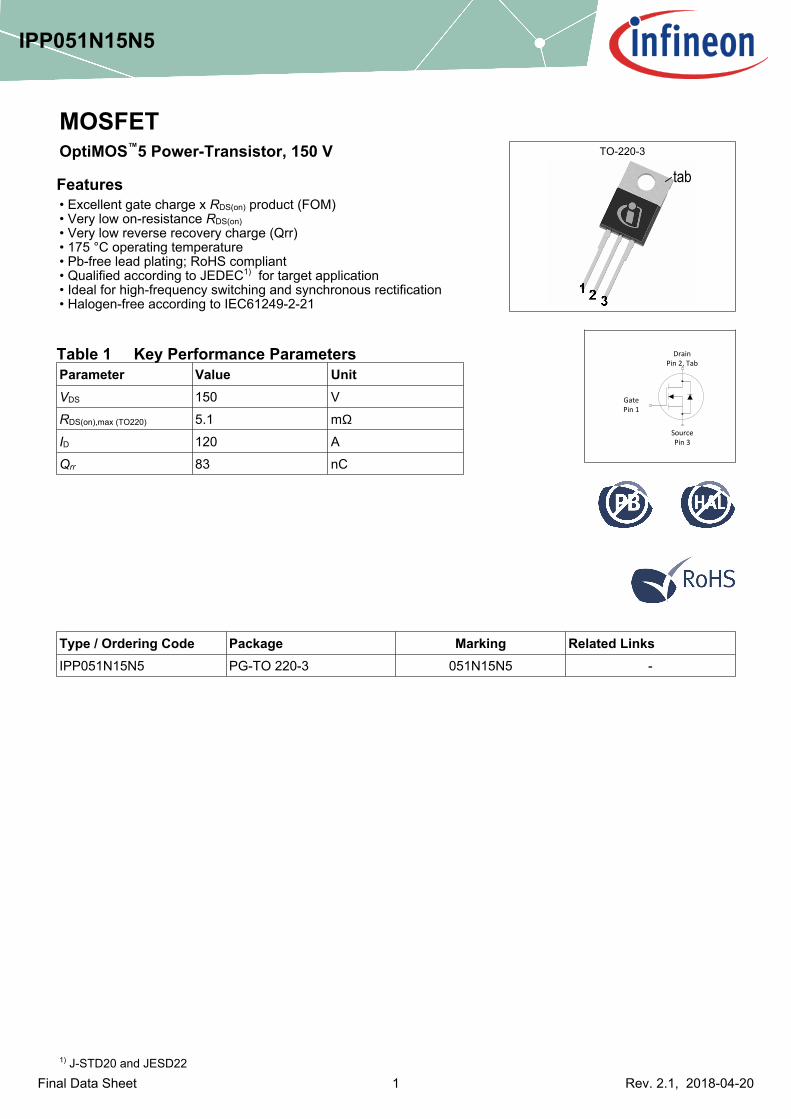
1 IPP051N15N5 Rev. 2.1, 2018-04-20 Final Data Sheet tab TO-220-3 Drain Pin 2, Tab Gate Pin 1 Source Pin 3 MOSFET OptiMOS ª 5 Power-Transistor, 150 V Features • Excellent gate charge x RDS(on) product (FOM) • Very low on-resistance RDS(on) • Very low reverse recovery charge (Qrr) • 175 °C operating temperature • Pb-free lead plating; RoHS compliant • Qualified according to JEDEC 1) for target application • Ideal for high-frequency switching and synchronous rectification • Halogen-free according to IEC61249-2-21 Table 1 Key Performance Parameters Parameter Value Unit VDS 150 V RDS(on),max (TO220) 5.1 mΩ ID 120 A Qrr 83 nC Type / Ordering Code Package Marking Related Links IPP051N15N5 PG-TO 220-3 051N15N5 - 1) J-STD20 and JESD22
Transcript of Datasheet IPP051N15N5 - Infineon Technologies
1
IPP051N15N5
Rev.2.1,2018-04-20Final Data Sheet
tabTO-220-3
DrainPin 2, Tab
GatePin 1
SourcePin 3
MOSFETOptiMOSª5Power-Transistor,150V
Features•ExcellentgatechargexRDS(on)product(FOM)•Verylowon-resistanceRDS(on)•Verylowreverserecoverycharge(Qrr)•175°Coperatingtemperature•Pb-freeleadplating;RoHScompliant•QualifiedaccordingtoJEDEC1)fortargetapplication•Idealforhigh-frequencyswitchingandsynchronousrectification•Halogen-freeaccordingtoIEC61249-2-21
Table1KeyPerformanceParametersParameter Value UnitVDS 150 V
RDS(on),max(TO220) 5.1 mΩ
ID 120 A
Qrr 83 nC
Type/OrderingCode Package Marking RelatedLinksIPP051N15N5 PG-TO 220-3 051N15N5 -
1) J-STD20 and JESD22
2
OptiMOSª5Power-Transistor,150VIPP051N15N5
Rev.2.1,2018-04-20Final Data Sheet
TableofContentsDescription . . . . . . . . . . . . . . . . . . . . . . . . . . . . . . . . . . . . . . . . . . . . . . . . . . . . . . . . . . . . . . . . . . . . . . . . . . . . . 1
Maximum ratings . . . . . . . . . . . . . . . . . . . . . . . . . . . . . . . . . . . . . . . . . . . . . . . . . . . . . . . . . . . . . . . . . . . . . . . . 3
Thermal characteristics . . . . . . . . . . . . . . . . . . . . . . . . . . . . . . . . . . . . . . . . . . . . . . . . . . . . . . . . . . . . . . . . . . . . 3
Electrical characteristics . . . . . . . . . . . . . . . . . . . . . . . . . . . . . . . . . . . . . . . . . . . . . . . . . . . . . . . . . . . . . . . . . . . 3
Electrical characteristics diagrams . . . . . . . . . . . . . . . . . . . . . . . . . . . . . . . . . . . . . . . . . . . . . . . . . . . . . . . . . . . 5
Package Outlines . . . . . . . . . . . . . . . . . . . . . . . . . . . . . . . . . . . . . . . . . . . . . . . . . . . . . . . . . . . . . . . . . . . . . . . . 9
Revision History . . . . . . . . . . . . . . . . . . . . . . . . . . . . . . . . . . . . . . . . . . . . . . . . . . . . . . . . . . . . . . . . . . . . . . . . 10
Trademarks . . . . . . . . . . . . . . . . . . . . . . . . . . . . . . . . . . . . . . . . . . . . . . . . . . . . . . . . . . . . . . . . . . . . . . . . . . . 10
Disclaimer . . . . . . . . . . . . . . . . . . . . . . . . . . . . . . . . . . . . . . . . . . . . . . . . . . . . . . . . . . . . . . . . . . . . . . . . . . . . 10

3
OptiMOSª5Power-Transistor,150VIPP051N15N5
Rev.2.1,2018-04-20Final Data Sheet
1MaximumratingsatTA=25°C,unlessotherwisespecified
Table2MaximumratingsValues
Min. Typ. Max.Parameter Symbol Unit Note/TestCondition
Continuous drain current ID --
--
120115 A TC=25°C
TC=100°C
Pulsed drain current1) ID,pulse - - 480 A TC=25°CAvalanche energy, single pulse2) EAS - - 230 mJ ID=100A,RGS=25ΩGate source voltage VGS -20 - 20 V -
Power dissipation Ptot - - 300 W TC=25°C
Operating and storage temperature Tj,Tstg -55 - 175 °C IEC climatic category;DIN IEC 68-1: 55/175/56
2Thermalcharacteristics
Table3ThermalcharacteristicsValues
Min. Typ. Max.Parameter Symbol Unit Note/TestCondition
Thermal resistance, junction - case RthJC - 0.3 0.5 K/W -
Thermal resistance, junction - ambient,minimal footprint RthJA - - 62 K/W -
3ElectricalcharacteristicsatTj=25°C,unlessotherwisespecified
Table4StaticcharacteristicsValues
Min. Typ. Max.Parameter Symbol Unit Note/TestCondition
Drain-source breakdown voltage V(BR)DSS 150 - - V VGS=0V,ID=1mAGate threshold voltage VGS(th) 3.0 3.8 4.6 V VDS=VGS,ID=264µA
Zero gate voltage drain current IDSS --
0.110
1100 µA VDS=120V,VGS=0V,Tj=25°C
VDS=120V,VGS=0V,Tj=125°C
Gate-source leakage current IGSS - 1 100 nA VGS=20V,VDS=0V
Drain-source on-state resistance RDS(on)--
4.04.3
5.15.7 mΩ VGS=10V,ID=60A
VGS=8V,ID=30A
Gate resistance3) RG - 1.1 1.6 Ω -
Transconductance gfs 59 117 - S |VDS|>2|ID|RDS(on)max,ID=60A
1) See Diagram 32) See Diagram 133) Defined by design. Not subject to production test

4
OptiMOSª5Power-Transistor,150VIPP051N15N5
Rev.2.1,2018-04-20Final Data Sheet
Table5DynamiccharacteristicsValues
Min. Typ. Max.Parameter Symbol Unit Note/TestCondition
Input capacitance1) Ciss - 6000 7800 pF VGS=0V,VDS=75V,f=1MHzOutput capacitance1) Coss - 1500 1950 pF VGS=0V,VDS=75V,f=1MHzReverse transfer capacitance1) Crss - 34 60 pF VGS=0V,VDS=75V,f=1MHz
Turn-on delay time td(on) - 19.6 - ns VDD=75V,VGS=10V,ID=60A,RG,ext=1.6Ω
Rise time tr - 5.3 - ns VDD=75V,VGS=10V,ID=60A,RG,ext=1.6Ω
Turn-off delay time td(off) - 25.5 - ns VDD=75V,VGS=10V,ID=60A,RG,ext=1.6Ω
Fall time tf - 4.5 - ns VDD=75V,VGS=10V,ID=60A,RG,ext=1.6Ω
Table6Gatechargecharacteristics2)Values
Min. Typ. Max.Parameter Symbol Unit Note/TestCondition
Gate to source charge Qgs - 33 - nC VDD=75V,ID=60A,VGS=0to10VGate to drain charge1) Qgd - 16 24 nC VDD=75V,ID=60A,VGS=0to10VSwitching charge Qsw - 26 - nC VDD=75V,ID=60A,VGS=0to10VGate charge total1) Qg - 80 100 nC VDD=75V,ID=60A,VGS=0to10VGate plateau voltage Vplateau - 5.4 - V VDD=75V,ID=60A,VGS=0to10VOutput charge1) Qoss - 225 299 nC VDD=75V,VGS=0V
Table7ReversediodeValues
Min. Typ. Max.Parameter Symbol Unit Note/TestCondition
Diode continous forward current IS - - 120 A TC=25°CDiode pulse current IS,pulse - - 480 A TC=25°CDiode forward voltage VSD - 0.87 1.1 V VGS=0V,IF=60A,Tj=25°CReverse recovery time1) trr - 60 120 ns VR=75V,IF=60A,diF/dt=100A/µsReverse recovery charge1) Qrr - 83 166 nC VR=75V,IF=60A,diF/dt=100A/µs
1) Defined by design. Not subject to production test2) See ″Gate charge waveforms″ for parameter definition
5
OptiMOSª5Power-Transistor,150VIPP051N15N5
Rev.2.1,2018-04-20Final Data Sheet
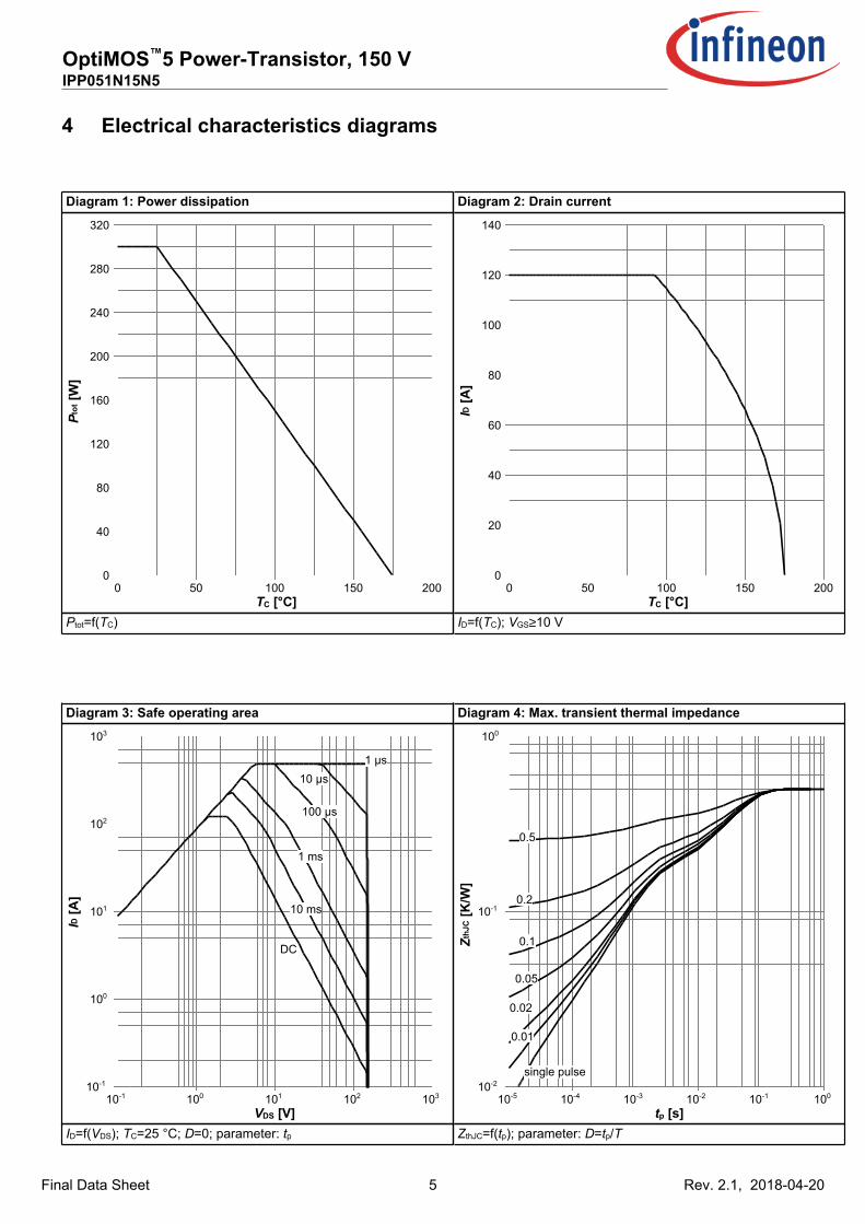
4Electricalcharacteristicsdiagrams
Diagram1:Powerdissipation
TC[°C]
Ptot[W
]
0 50 100 150 2000
40
80
120
160
200
240
280
320
Ptot=f(TC)
Diagram2:Draincurrent
TC[°C]
ID[A
]
0 50 100 150 2000
20
40
60
80
100
120
140
ID=f(TC);VGS≥10V
Diagram3:Safeoperatingarea
VDS[V]
ID[A
]
10-1 100 101 102 10310-1
100
101
102
103
1 µs
10 µs
100 µs
1 ms
10 ms
DC
ID=f(VDS);TC=25°C;D=0;parameter:tp
Diagram4:Max.transientthermalimpedance
tp[s]
ZthJC[K
/W]
10-5 10-4 10-3 10-2 10-1 10010-2
10-1
100
0.5
0.2
0.1
0.05
0.02
0.01
single pulse
ZthJC=f(tp);parameter:D=tp/T

6
OptiMOSª5Power-Transistor,150VIPP051N15N5
Rev.2.1,2018-04-20Final Data Sheet
Diagram5:Typ.outputcharacteristics
VDS[V]
ID[A
]
0 1 2 3 4 50
50
100
150
200
250
300
350
400
8 V
10 V
7 V
6 V
5.5 V
5 V
4.5 V
ID=f(VDS);Tj=25°C;parameter:VGS
Diagram6:Typ.drain-sourceonresistance
ID[A]
RDS(on
) [m
Ω]
0 50 100 150 200 250 300 350 4000
2
4
6
8
10
5.5 V
6 V
7 V
8 V
10 V
8 V
10 V
RDS(on)=f(ID);Tj=25°C;parameter:VGS
Diagram7:Typ.transfercharacteristics
VGS[V]
ID[A
]
0 2 4 6 80
50
100
150
200
250
300
350
400
175 °C 25 °C
ID=f(VGS);|VDS|>2|ID|RDS(on)max;parameter:Tj
Diagram8:Typ.forwardtransconductance
ID[A]
gfs [S]
0 40 80 1200
40
80
120
160
200
gfs=f(ID);Tj=25°C
7
OptiMOSª5Power-Transistor,150VIPP051N15N5
Rev.2.1,2018-04-20Final Data Sheet
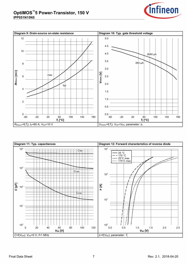
Diagram9:Drain-sourceon-stateresistance
Tj[°C]
RDS(on
) [m
Ω]
-60 -20 20 60 100 140 1800
2
4
6
8
10
12
max
typ
RDS(on)=f(Tj);ID=60A;VGS=10V
Diagram10:Typ.gatethresholdvoltage
Tj[°C]
VGS(th) [V]
-60 -20 20 60 100 140 1800.0
0.5
1.0
1.5
2.0
2.5
3.0
3.5
4.0
4.5
5.0
2640 µA
264 µA
VGS(th)=f(Tj);VGS=VDS;parameter:ID
Diagram11:Typ.capacitances
VDS[V]
C[p
F]
0 20 40 60 80 100 120100
101
102
103
104Ciss
Coss
Crss
C=f(VDS);VGS=0V;f=1MHz
Diagram12:Forwardcharacteristicsofreversediode
VSD[V]
IF [A]
0.0 0.5 1.0 1.5 2.0 2.5100
101
102
103
25 °C175 °C25°C max175°C max
IF=f(VSD);parameter:Tj
8
OptiMOSª5Power-Transistor,150VIPP051N15N5
Rev.2.1,2018-04-20Final Data Sheet
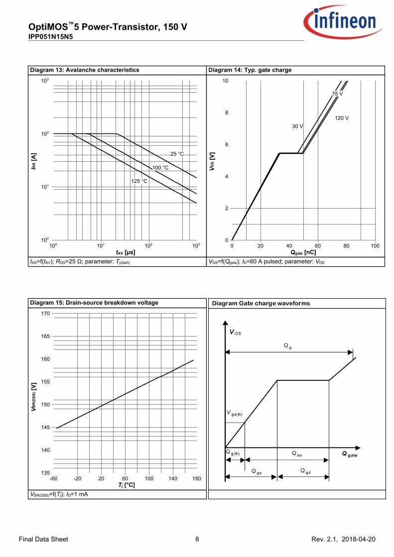
Diagram13:Avalanchecharacteristics
tAV[µs]
IAS [A]
100 101 102 103100
101
102
103
25 °C
100 °C
125 °C
IAS=f(tAV);RGS=25Ω;parameter:Tj(start)
Diagram14:Typ.gatecharge
Qgate[nC]
VGS [V]
0 20 40 60 80 1000
2
4
6
8
10
120 V
75 V
30 V
VGS=f(Qgate);ID=60Apulsed;parameter:VDD
Diagram15:Drain-sourcebreakdownvoltage
Tj[°C]
VBR(DSS
) [V]
-60 -20 20 60 100 140 180135
140
145
150
155
160
165
170
VBR(DSS)=f(Tj);ID=1mA
Diagram Gate charge waveforms
9
OptiMOSª5Power-Transistor,150VIPP051N15N5
Rev.2.1,2018-04-20Final Data Sheet
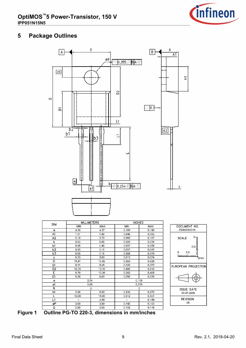
5PackageOutlines
Figure1OutlinePG-TO220-3,dimensionsinmm/inches

10
OptiMOSª5Power-Transistor,150VIPP051N15N5
Rev.2.1,2018-04-20Final Data Sheet
RevisionHistoryIPP051N15N5
Revision:2018-04-20,Rev.2.1
Previous Revision
Revision Date Subjects (major changes since last revision)
2.0 2016-02-01 Release of final version
2.1 2018-04-20 Update tf, td(off), trr and Qrr
TrademarksofInfineonTechnologiesAG
AURIX™,C166™,CanPAK™,CIPOS™,CoolGaN™,CoolMOS™,CoolSET™,CoolSiC™,CORECONTROL™,CROSSAVE™,DAVE™,DI-POL™,DrBlade™,EasyPIM™,EconoBRIDGE™,EconoDUAL™,EconoPACK™,EconoPIM™,EiceDRIVER™,eupec™,FCOS™,HITFET™,HybridPACK™,Infineon™,ISOFACE™,IsoPACK™,i-Wafer™,MIPAQ™,ModSTACK™,my-d™,NovalithIC™,OmniTune™,OPTIGA™,OptiMOS™,ORIGA™,POWERCODE™,PRIMARION™,PrimePACK™,PrimeSTACK™,PROFET™,PRO-SIL™,RASIC™,REAL3™,ReverSave™,SatRIC™,SIEGET™,SIPMOS™,SmartLEWIS™,SOLIDFLASH™,SPOC™,TEMPFET™,thinQ™,TRENCHSTOP™,TriCore™.
TrademarksupdatedAugust2015
OtherTrademarks
Allreferencedproductorservicenamesandtrademarksarethepropertyoftheirrespectiveowners.
WeListentoYourCommentsAnyinformationwithinthisdocumentthatyoufeeliswrong,unclearormissingatall?Yourfeedbackwillhelpustocontinuouslyimprovethequalityofthisdocument.Pleasesendyourproposal(includingareferencetothisdocument)to:[email protected]
PublishedbyInfineonTechnologiesAG81726München,Germany©2018InfineonTechnologiesAGAllRightsReserved.
LegalDisclaimerTheinformationgiveninthisdocumentshallinnoeventberegardedasaguaranteeofconditionsorcharacteristics(“Beschaffenheitsgarantie”).
Withrespecttoanyexamples,hintsoranytypicalvaluesstatedhereinand/oranyinformationregardingtheapplicationoftheproduct,InfineonTechnologiesherebydisclaimsanyandallwarrantiesandliabilitiesofanykind,includingwithoutlimitationwarrantiesofnon-infringementofintellectualpropertyrightsofanythirdparty.Inaddition,anyinformationgiveninthisdocumentissubjecttocustomer’scompliancewithitsobligationsstatedinthisdocumentandanyapplicablelegalrequirements,normsandstandardsconcerningcustomer’sproductsandanyuseoftheproductofInfineonTechnologiesincustomer’sapplications.Thedatacontainedinthisdocumentisexclusivelyintendedfortechnicallytrainedstaff.Itistheresponsibilityofcustomer’stechnicaldepartmentstoevaluatethesuitabilityoftheproductfortheintendedapplicationandthecompletenessoftheproductinformationgiveninthisdocumentwithrespecttosuchapplication.
InformationForfurtherinformationontechnology,deliverytermsandconditionsandpricespleasecontactyournearestInfineonTechnologiesOffice(www.infineon.com).
WarningsDuetotechnicalrequirements,componentsmaycontaindangeroussubstances.Forinformationonthetypesinquestion,pleasecontactthenearestInfineonTechnologiesOffice.TheInfineonTechnologiescomponentdescribedinthisDataSheetmaybeusedinlife-supportdevicesorsystemsand/orautomotive,aviationandaerospaceapplicationsorsystemsonlywiththeexpresswrittenapprovalofInfineonTechnologies,ifafailureofsuchcomponentscanreasonablybeexpectedtocausethefailureofthatlife-support,automotive,aviationandaerospacedeviceorsystemortoaffectthesafetyoreffectivenessofthatdeviceorsystem.Lifesupportdevicesorsystemsareintendedtobeimplantedinthehumanbodyortosupportand/ormaintainandsustainand/orprotecthumanlife.Iftheyfail,itisreasonabletoassumethatthehealthoftheuserorotherpersonsmaybeendangered.