Datasheet FS3862 - ic-fortune.com
32
REV. 1.3 FS3862-DS-13_EN MAY. 2007 Datasheet FS3862 8-bit MCU with 1k program EPROM, 64-byte SRAM, 5-bit I/O port, Intelligent Charger Management Controller
Transcript of Datasheet FS3862 - ic-fortune.com
REV. 1.3 FS3862-DS-13_EN MAY. 2007
Datasheet
FS3862 8-bit MCU with 1k program EPROM, 64-byte SRAM, 5-bit I/O port, Intelligent Charger Management Controller

FS3862
Fortune Semiconductor Corporation 富晶電子股份有限公司
28F., No.27, Sec. 2, Zhongzheng E. Rd., Danshui Town, Taipei County 251, Taiwan Tel.:886-2-28094742 Fax:886-2-28094874 www.ic-fortune.com
This manual contains new product information. Fortune Semiconductor Corporation reserves the rights to modify the product specification without further notice. No liability is assumed by Fortune Semiconductor Corporation as a result of the use of this product. No rights under any patent accompany the sale of the product.
Rev. 1.3 2/32
FS3862
Contents
1. GENERAL DESCRIPTION................................................................................................................... 5 2. FEATURES.......................................................................................................................................... 5 3. APPLICATIONS................................................................................................................................... 5 4. ORDERING INFORMATION................................................................................................................. 5 5. PIN CONFIGURATIONS ...................................................................................................................... 6
5.1 FS3862 SSOP16 Package........................................................................................................ 6 5.2 Pin Description ....................................................................................................................... 6
6. FUNCTIONAL BLOCK DIAGRAM ....................................................................................................... 7 7. ELECTRICAL CHARACTERISTICS..................................................................................................... 8
7.1 Absolute Maximum Ratings.................................................................................................... 8 7.2 D.C. Characteristics (VDD= 5.0V, Ta=25°C, unless otherwise noted) ..................................... 8
8. FUNCTIONAL DESCRIPTION ............................................................................................................. 9 8.1 Typical Charging Conditions and Phases .............................................................................. 9 8.2 Charging Application Circuit .................................................................................................11 8.3 Operation Flow Chart of Charging Application .....................................................................13 8.4 The Architecture of FS3862 ...................................................................................................13
9. MEMORY ORGANIZATION.................................................................................................................14 9.1 Program Memory Organization..............................................................................................14 9.2 Data Memory Structure ..........................................................................................................14 9.3 System Special Registers......................................................................................................15 9.4 Peripheral Special Registers .................................................................................................15 9.5 Power System ........................................................................................................................16 9.6 CCCTL....................................................................................................................................16 9.7 CVCTL ....................................................................................................................................17 9.8 Comparator ............................................................................................................................18 9.9 8-bits Timer ............................................................................................................................19 9.10 LED and General I/O ..............................................................................................................20 9.11 External Reset........................................................................................................................20
10. CALIBRATION....................................................................................................................................21 11. HALT AND SLEEP MODES ................................................................................................................21
11.1 Halt Mode ...............................................................................................................................21 11.2 Sleep Mode.............................................................................................................................21
12. INSTRUCTION SET............................................................................................................................21 12.1 Instruction Set Summary .......................................................................................................22
Rev. 1.3 3/32

FS3862
12.2 Struction Description.............................................................................................................23 13. PACKAGE INFORMATION .................................................................................................................30
13.1 Package Outline & Dimensions .............................................................................................30 14. REVISION HISTORY...........................................................................................................................32
Rev. 1.3 4/32

FS3862
1. General Description The FS3862 is a low-cost high-performance Li+ single-cell 4.2v/4.1v battery charger control IC which includes all the required constant-current and constant-voltage regulations of charge functions addressed for linear charger mode operations in typical four phases: pre-charging conditioning, constant current, constant voltage, and charge terminations (usually based on the minimum current reached). The maintenance re-charge (or called post-charge stage) proceeds if the full-charged battery voltage is once again lower than the desired full-capacity voltage because of consumptions of its capacity which occurs either at the battery’s internal voltage drop across its terminals, or at the use of the battery. This chip with built-in 8-bit RISC-type MCU with 1K-word OTP PROM and 64-Byte data RAM employs a minimum numbers of external transistor and passive resistor & capacitor devices to fulfill complete charger implementations at cost-effective solutions. The available 16-pin SSOP-16 package is offered for balanced area and cost effective requirements for size-sensitive applications. The FS3862 is suitable for the control of charge sequences of a variety of portable battery-powered applications, such as cellular phone’s travel and base charger devices, digital camera, digital-video camcorder (DV), MP3 player ,etc.
2. Features Ideal for the Li-ion/polymer Single-Cell 4.2v/4.1v charge control. Built-in 8-bit RISC-typed MCU with 1K-word OTP program ROM and 64-Byte data RAM. Integrated voltage and current regulation with programmable charge current. Supports typical Li+ battery’s charge sequences such as pre-charge (trickle-mode charge), C-C (constant-current charge), C-V (constant-voltage charge), charge terminations, and re-charge operations. Batter than 1% charge voltage regulation accuracy. Charge operation can be monitored by the external host through the general I/O data bus. 2 LED output for charge status. Optional Temp and battery ID input through voltage sense input. Low-cost peripheral components of capacitor and resistor combinations for minimum BOM cost in manufacturing considerations. Development kit of LQFP-64 ICE evaluation (EV) board and reference charge program available for prototype design and facilitating debug use. SSOP-16 Package.
3. Applications Cellular phone external base or built-in charger MP3 player External charger through USB Digital still camera (DSC) Digital video camcorder (DV)
4. Ordering Information
Product Number Description Package Type FS3862-nnnV-POA Customer’s compiled hex code can be
programmed by FSC or customer itself into EPROM at factory before shipping.
SSOP-16
Note1: Code number (nnnV) is assigned for customer. Note2: Code number (nnn = 001~999); Version (V = A~Z).
Rev. 1.3 5/32

FS3862
5. Pin Configurations
5.1 FS3862 SSOP16 Package
5.2 Pin Description
Name I/O Pin No Description SNS I 1 Current sensing using an external sensing resistor RSNS VCC I 2 Supply voltage
RST_/VPP I 3 Active low reset or as active high OTP program write
TEST I 4 Test mode input. Test=1 is the normal mode. Test Mode is initiated while Test=0 before reset. This pin is suggested pulled inactive high for regular operation without Test Mode.
GPIO[0] I/O 5 General purpose bi-directional I/O pin 0 GPIO[1] I/O 6 General purpose bi-directional I/O pin 1 GPIO[2] I/O 8 General purpose bi-directional I/O pin 2
GND 7 Ground
OSC I 9 Oscillator input. Connect to an external resistor R=200kΩ, the oscillator frequency is around 4.5MHz
NC - 10 No connection. LED0 O 11 Source or sink LED0 display LED1 O 12 Source or sink LED1 display
TS I 13 Battery temperature sensing input
VBATID I 14 Battery ID-type selected by the voltage drop across the series resistor. Battery ID is for identification of either thick, thin battery or other selected types
VBAT I 15 Battery input voltage CC O 16 Charge control output to drive pass transistor
Rev. 1.3 6/32
FS3862
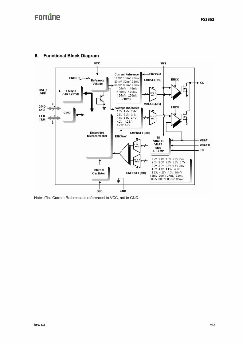
6. Functional Block Diagram
Note1:The Current Reference is referenced to VCC, not to GND.
Rev. 1.3 7/32
FS3862
7. Electrical Characteristics
7.1 Absolute Maximum Ratings
Parameter Rating Unit Supply Voltage to Ground Potential -0.3 to 6.0 V Applied Input/Output Voltage VSS-0.3 to VDD+0.3 V Ambient Operating Temperature -20 to +70 °C Storage Temperature -55 to +150 °C Soldering Temperature, Time 260°C, 10 Sec ESD immunity, Human Body Mode / Machine Model ≧2kV / 200V Latch-up immunity ≧100mA
7.2 D.C. Characteristics (VDD= 5.0V, Ta=25°C, unless otherwise noted)
Symbol Parameter Test Conditions Min. Typ. Max. Unit
VCC Recommend Operation Power Voltage 4.35 5.0 5.5 V
ICC1 Input VCC current on charge mode (regular operation)
VCC > VCC (min) 1 3 mA
ICC2 Input VCC current on sleep mode. VCC > VCC (min) 25 uA
IBAT Input VBAT current on sleep mode
VBAT>VCC; VCC is OFF VBAT=4.2V; VCC disconnect 100 uA
VIH Digital I/O input high voltage
VCC Voltage applied 4.35v to 5.5v 2.5 5.5 V
VIL Digital I/O input low voltage
VCC Voltage applied 4.35v to 5.5v -0.3 0.8 V
Digital I/O output sink current
Output sink current of digital I/O pins set as output mode 20 mA
Isink LED I/O output sink current
Output sink current of LED I/O pins set as output mode 20 mA
Digital I/O output source current
Output source current of digital I/O pins set as input mode 0.1 mA
Isource LED I/O output source current
Output source current of LED I/O pins set as input mode 10 mA
Vref Internal reference voltage The oltage is defined by selected register
VREF (Target) -0.05
VREF ( Target)
VREF (Target) +0.05
V
Vcref Build in reference voltage temperature coefficient TA=0~60°C 150 ppm/°C
FRC Internal RC oscillator External R=650kΩ 150 kHz
Rev. 1.3 8/32

FS3862
8. Functional Description
8.1 Typical Charging Conditions and Phases
The FS3862 uses flexible control schemes of charger’s current and voltage regulations in conjunction with the built-in 8-bit RISC-type MCU core running at typical 100kHz for desired charge sequence controls during its operations. It is embedded with the constant-current and constant-voltage regulations as well as the additional facilities of PWM voltages for user-defined intermediate voltage levels used for various applications. The external sensing resistors together with built-in parameters of the 8-bit MCU enable the device performing charge cycle operations through selections of small to larger charge current’s amounts primarily for Li+ battery’s linear mode charge applications, where the pulse-mode charging can be implemented using the internal hardware to control the charge sequences as implemented by the built-in MCU program code for various charger applications.
Fig.8-1 Typical Charge Profile
The typical Li+ charge steps are mainly four stages to conduct: ˙Pre-charge conditioning (or called trickle-mode charge, as the Phase-0 stage): where the low-voltage discharged battery typical lower than 3.0v (or 2.8v, depending on how the battery’s parameters are set) gets wake-up by applying typical 1/10 of full-rate charge current (a small amount of selectable charge current, also called trickle current, such as 85mA of 850mA charge current ) until reaching the threshold voltage 3.0v. If the trickle current has been applied to the battery for more than 30 minutes by timer’s measurement and not reaching the required 3.0v, it could be detected as bad battery without continuing to the next step of charge operations.
Rev. 1.3 9/32

FS3862
˙Constant current charge (as Phase-1, referred as C-C stage): where the programmable constant current ranging from typical 250mA to 1,050mA is applied to the battery, until the battery voltage reaches to the full-level at 4.2v or similar value such as 4.1v or even 4.0v. Some applications require the constant current charge at USB current of 500mA when its power line at 5v is applied, and such charge stage can be implemented with selection of the current regulation at 500mA by setting the corresponding C-C reference bit and current select values at the specified control registers, as explained in details descriptions in later section. ˙Constant voltage charge (shown as Phase-2, referred as C-V stage): using the regulated voltage at 4.2v reached at the constant current charge stage until the termination condition is met at the final low termination top-off current at smaller amount (such as 100mA which can be programmable to select), and then charges to the full capacity when termination occurs. Selections of the C-V charge’s voltage level can be made with corresponding C-V enable and voltage select values at the individual specified control registers. ˙Maintenance re-charge (shown as Phase-3 stage): can be called Post-charge stage, which is to resume charges to the battery when the battery’s voltage drops is more than 0.1v (i.e. The battery terminal voltage becomes 4.10v or less from its full voltage at 4.20v) as a result of the internal resistor during its idle state through some time. If the battery has been taken off for use on its portable device, there is no re-charge check to conduct since the state transitions to the initial state without the battery itself. In some other cases, the preliminary charge stage which can be conducted as one step prior to the phase-0 to assure the battery to be through the charge sequences has working functions to perform. This stage would involve in applying constant-voltage charge pulses at defined level of 4.0v or so to the battery, which was examined to determine if it’s at low voltage of 2.5v or less. The charge pulses applied to the battery for a short period of 15 intervals with 10 seconds high (at 4.0v voltage beats) and 5 seconds low (ground) each to examine if the battery voltage still remain low at 2.5v or less, which is then considered as defective and should be discarded. Sometimes another additional check-up procedure follows the termination of the C-V stage to assure the battery in proper waiting stage for operation. That is to have the battery stay idle from its charge termination at full voltage of 4.20v (or 4.1v, depending on the battery’s manufacturer’s parameters). Then the battery stays in for additional 10 (or 15, also an adjustable parameter) minutes, and then its voltage is examined to assure the terminal voltage won’t be decreased to lower than 4.05v (or 3.95v if the situation prevails), then the battery is also determined as a defective one without reliable performance since it could be losing more than 0.15v within a short period of just 10 (or 15) minutes. These check-up procedures are optional. In brief summary, the typical Li+ battery charger’s procedures could be summarized in the following few steps: pre-charge conditioning, constant-current (C-C), constant voltage (C-V) stage, charge termination and monitor to re-charge, etc. There might have some individual charge’s current- or voltage-control schemes within the designated step to perform.
Rev. 1.3 10/32
FS3862
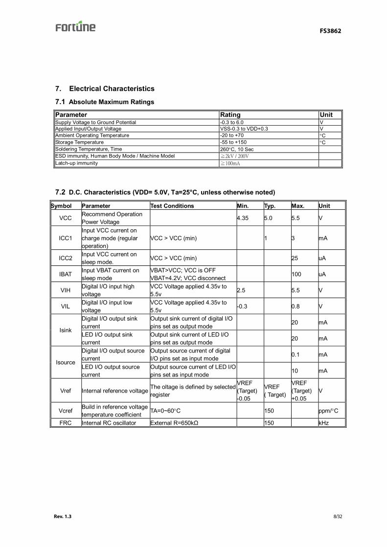
8.2 Charging Application Circuit
Fig.8-2 FS3862 Type Application Circuit
Fig.8-3 FS3862 Host Control Application Circuit
Rev. 1.3 11/32
FS3862
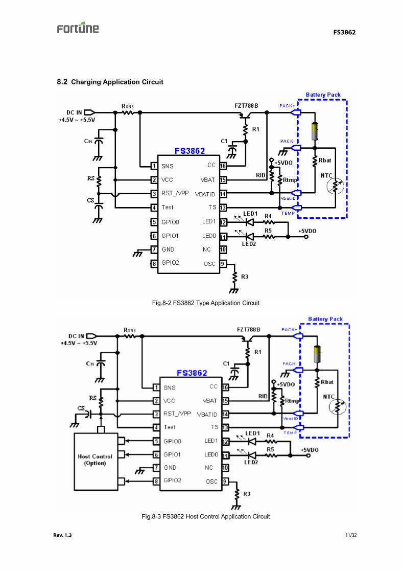
Fig.8-4 FS3862 P-MOS Application Circuit
The Fig.8-2 shows the typical FS3862 application circuit used at base or travel charger devices of a variety of cellular phone and other portable devices. The above application circuitry shows the chip connected with an one-cell Li+ 4.2v battery, which features battery ID (at the VBATID input pin) and temperature sense output (at TS pin) for relevant controls. Interface to external host is optional at the general I/O bus pins with connections to the host side which commands the base charger with monitor facilities to control the charger operations. The use of PNP or PMOS (Fig.8-4) as the pass transistor realizes the control of C-C and/or C-V mode current/voltage regulations.
Rev. 1.3 12/32
FS3862
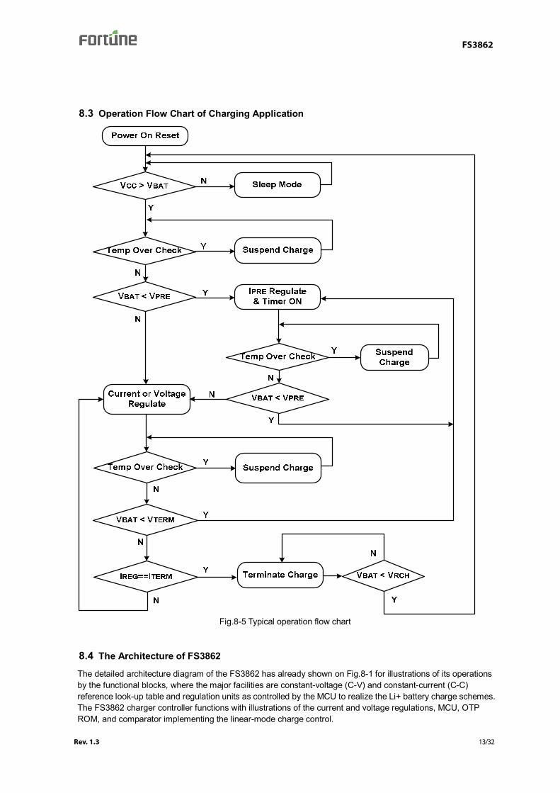
8.3 Operation Flow Chart of Charging Application
Fig.8-5 Typical operation flow chart
8.4 The Architecture of FS3862
The detailed architecture diagram of the FS3862 has already shown on Fig.8-1 for illustrations of its operations by the functional blocks, where the major facilities are constant-voltage (C-V) and constant-current (C-C) reference look-up table and regulation units as controlled by the MCU to realize the Li+ battery charge schemes. The FS3862 charger controller functions with illustrations of the current and voltage regulations, MCU, OTP ROM, and comparator implementing the linear-mode charge control.
Rev. 1.3 13/32

FS3862
9. Memory Organization
FS3862 has an 1k x 16bits program memory space and a 6 level depth 12bits Stack Register. The Start up/Reset Vector is at 0x0000H. When FS3862 is started or its program is reset, the Program Counter will point to Reset Vector. The Interrupt Vector is at 0x0004H. No matter what ISR is processed, the Program Counter will point to Interrupt Vector.
9.1 Program Memory Organization
CPU has a 10-bit program counter capable of address up to 1k x 16 program memory space. The reset vector is at 0000H and the interrupt vector is at 0004H.
9.2 Data Memory Structure
FS3862 has a 64 byte SRAM for Data Memory. The data memory is partitioned into three parts. The area with address 00h~07h is reserved for system special registers, such as indirect address, indirect address pointer, status register, working register, interrupt flag, interrupt control register. The address 08h~1Fh areas are peripheral special registers, such as I/O ports, timer, ADC, signal conditional network control register, LCD driver. The address 80h~BFh areas are general data memory.
Start Address End Address Data Memory
0X00H 0X07H System Special Registers
0X08H 0X1FH Peripheral Special Registers
0X80H 0XBFH General Data Memory
Rev. 1.3 14/32
FS3862
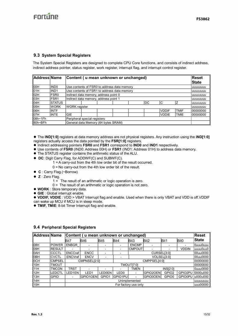
9.3 System Special Registers
The System Special Registers are designed to complete CPU Core functions, and consists of indirect address, indirect address pointer, status register, work register, interrupt flag, and interrupt control register. Address Name Content ( u mean unknown or unchanged) Reset
State 00H IND0 Use contents of FSR0 to address data memory uuuuuuuu 01H IND1 Use contents of FSR1 to address data memory uuuuuuuu 02H FSR0 Indirect data memory, address point 0 uuuuuuuu 03H FSR1 Indirect data memory, address point 1 uuuuuuuu 04H STATUS DC C Z uuuuuuuu 05H WORK WORK register uuuuuuuu 06H INTF VDDIF TMIF 00000000 07H INTE GIE VDDIE TMIE 00000000 08h~1Fh Peripheral special registers 80h~BFh General data Memory (64 bytes SRAM)
The IND[1:0] registers at data memory address are not physical registers. Any instruction using the IND[1:0] registers actually access the data pointed by the FSR[1:0] registers.
Indirect addressing pointers FSR0 and FSR1 correspond to IND0 and IND1 respectively. Use contents of FSR0 (IND0: Address 00H) or FSR1 (IND1: Address 01H) to address data memory. The STATUS register contains the arithmetic status of the ALU. DC: Digit Carry Flag, for ADDWF(C) and SUBWF(C).
1 = A carry-out from the 4th low order bit of the result occurred. 0 = No carry-out from the 4th low order bit of the result.
C : Carry Flag.(~Borrow) Z : Zero Flag.
1 = The result of an arithmetic or logic operation is zero. 0 = The result of an arithmetic or logic operation is not zero.
WORK : Store temporary data. GIE : Global interrupt enable. VDDIF, VDDIE : VDD > VBAT Interrupt flag and enable. Used when there is only VBAT and VDD is off.VDDIF
can wake up MCU if MCU is in sleep mode. TMIF, TMIE: 8-bit Timer Interrupt flag and enable.
9.4 Peripheral Special Registers
Content ( u mean unknown or unchanged) Address Name Bit7 Bit6 Bit5 Bit4 Bit3 Bit2 Bit1 Bit0
Reset State
08H POWER ENBGR_ - - - ENCMP - - - 0uuu0uuu09H RESULT - - - - CMPOUT - - VDDIN uuuu0uu00AH CCCTL ENCCref ENCC - - CURSEL[3:0] 00uu00000BH CVCTL ENCVref ENCV - - VOLSEL[3:0] 00uu00000CH CMPSEL CMPNSEL[2:0] CMPPSEL[4:0] 0000000010H TMOUT TMOUT[7:0] 0000000011H TMCON TRST - - - TMEN INS[2:0] 0uuu000012H LEDCTL LED1EN LED1 LED0EN LED0 - GPIO2OEN GPIO2 GPIO2PU 0000u00013H GPIO - GPIO1OEN GPIO1 GPIO1PU - GPIO0OEN GPIO0 GPIO0PU u000u00014H Unimplemented uuuuuuuu15H For factory use only uuu00000
Rev. 1.3 15/32

FS3862
9.5 Power System
Address Name Content ( u mean unknown or unchanged) Reset State
08H POWER ENBGR ENCMP 0uuu0uuu
ENBGR_=0 is enable,”1” is Disable; This bit is active LOW enable. ENBGR_=0 is enable Voltage and Current and Comparator regulations. Before enabling ENCCref or ENCVref and ENCMP, ENBGR_ must be set.
9.6 CCCTL
Address Name Content ( u mean unknown or unchanged) Reset State
0AH CCCTL ENCCref ENCC - - CURSEL[3:0] 00uu0000
The Current Reference is referenced to VCC, not to GND. Enable ENCCref can be constant current regulation reference current. ENCC=1 Enables the constant current regulation for constant current charge with desired current amount
selected.
Rev. 1.3 16/32
FS3862
Select CURSEL[3:0] set constant current regulation reference current. The regulation current accuracy is ±10% (unless otherwise noted). If Enables ENCC, ENCV must be Disables. Current sensing using an external sensing resistor RSNS=0.22ohm. Through selecting VRSNS , you can decide the charge current. ( VRSNS/ RSNS=Charge Current) is the formula
of VRSNS converting to the current value.
CURSEL[3:0] 0000 0001 0010 0011 0100 0101 0110 0111
VRSNS Select 10mV ±4mV
15mV ±4mV
20mV ±4mV
27mV ±4mV
32mV ±4mV
38mV ±4mV
60mV ±6mV
83mV ±8mV
換算成電流值 27mA ~64mA
50mA ~86mA
73mA ~109mA
105mA~141mA
127mA~164mA
155mA ~191mA
245mA ~300mA
341mA ~414mA
CURSEL[3:0] 1000 1001 1010 1011 1100 1101 1110 1111
VRSNS Select 95mV ±9mV
105mV±10mV
115mV±11mV
150mV±15mV
175mV±17mV
195mV ±20mV
220mV ±22mV
240mV ±24mV
換算成電流值 391mA ~473mA
432mA~523mA
473mA~573mA
614mA~750mA
718mA~873mA
795mA ~977mA
900mA ~1100mA
982mA ~1200mA
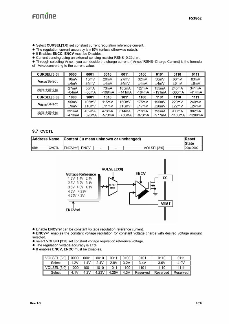
9.7 CVCTL
Address Name Content ( u mean unknown or unchanged) Reset State
0BH CVCTL ENCVref ENCV - - VOLSEL[3:0] 00uu0000
Enable ENCVref can be constant voltage regulation reference current. ENCV=1 enables the constant voltage regulation for constant voltage charge with desired voltage amount
selected. select VOLSEL[3:0] set constant voltage regulation reference voltage. The regulation voltage accuracy is ±1%. If enables ENCV, ENCC must be Disables.
VOLSEL [3:0] 0000 0001 0010 0011 0100 0101 0110 0111
Select 1.2V 1.4V 2.4V 2.8V 3.2V 3.4V 3.6V 4.0V VOLSEL [3:0] 1000 1001 1010 1011 1100 1101 1110 1111
Select 4.1V 4.2V 4.23V 4.25V 4.3V Reserved Reserved Reserved
Rev. 1.3 17/32

FS3862
9.8 Comparator
Address Name Content ( u mean unknown or unchanged) Reset State
08H POWER ENCMP 0uuu0uuu09H RESULT CMPOUT VDDIN uuuu0uu00CH CMPSEL CMPNSEL[2:0] CMPPSEL [4:0] 00000000
The comparator enable bit enables the internal comparator for comparison between the measured input parameters (such as the battery voltage, sensed charged current, battery temperature, etc.) and the pre-set current or voltage values selected by the comparator select CMPPSEL[4:0] (ADDRESS 0CH).
Also refer to ENCMP (ADDRESS 08H) and CMPOUT (ADDRESS 09H) register bits. Enable ENCMP can be constant current and voltage regulation reference current. The bit CMPOUT is the compared output and would be set high on comparator’s measured input value (like
current across the sense resistor Rsns with selecting the desired measured item by setting the CMPNSEL[2:0]) match exactly with the positive input of the selected reference value.
The VDDIN status indicator (Read Only) of supply voltage VCC greater than VBAT, i.e. VDDIN is set high when VCC > VBAT. If there is no VCC and only the VBAT of battery is connected, then the VDDIN is set inactive low.
CMPNSEL[2:0] select comparator negative input.
CMPNSEL [2:0] 000 001 010 011 100 101 110 111 Select TS VBATID VBAT SNS ICTEMP Reserved Reserved Reserved
TS The voltage of external thermistor, with either PTC (positive temperature) or NTC (negative
temperature) coefficient, and is compared with VPWM for temperature measurements and subsequent control actions.
VBATID The voltage of external Battery ID, and is compared with VPWM for determining the battery’s types before charges.
VBAT Battery voltage and will be compared with 2.5V, 2.6V, 3.0V, 3.9V,….4.25V, 4.3V, also shown on the voltage regulations.
SNS The current sensing voltage and will be compared with the 50mA, 100mA, 150mA to determine the termination current.
Rev. 1.3 18/32
FS3862
CMPPSEL[4:0] select comparator positive input. CMPPSEL [4:0] 00000 00001 00010 00011 00100 00101 00110 00111
Select Reserved 1.2V 1.4V 1.5V 2.0V 2.4V 2.5V 2.6V CMPPSEL [4:0] 01000 01001 01010 01011 01100 01101 01110 01111
Select 2.8V 3.0V 3.1V 3.2V 3.3V 3.4V 3.6V 3.9V CMPPSEL [4:0] 10000 10001 10010 10011 10100 10101 10110 10111
Select 4.0V 4.10V 4.15V 4.20V 4.23V 4.25V 4.3V 10mV ±4mV
CMPPSEL [4:0] 11000 11001 11010 11011 11100 11101 11110 11111
Select 15mV ±4mV
20mV±4mV
27mV ±4mV
32mV±4mV
38mV ±4mV
60mV±6mV
83mV ±8mV
95mV ±9mV
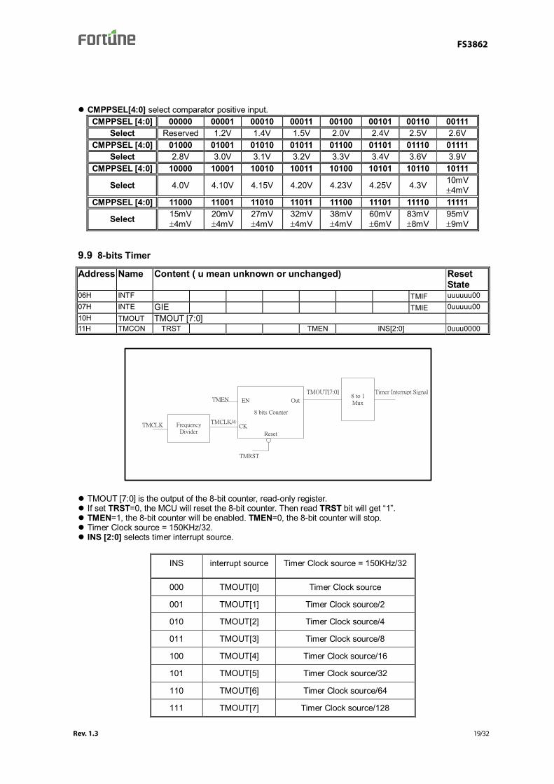
9.9 8-bits Timer
Address Name Content ( u mean unknown or unchanged) Reset State
06H INTF TMIF uuuuuu0007H INTE GIE TMIE 0uuuuu0010H TMOUT TMOUT [7:0] 11H TMCON TRST TMEN INS[2:0] 0uuu0000
8 bits Counter
Reset
EN
CK
Out8 to 1Mux
Timer Interrupt SignalTMOUT[7:0]
TMRST
TMEN
FrequencyDivider
TMCLK/4TMCLK
TMOUT [7:0] is the output of the 8-bit counter, read-only register. If set TRST=0, the MCU will reset the 8-bit counter. Then read TRST bit will get “1”. TMEN=1, the 8-bit counter will be enabled. TMEN=0, the 8-bit counter will stop. Timer Clock source = 150KHz/32. INS [2:0] selects timer interrupt source.
INS interrupt source Timer Clock source = 150KHz/32
000 TMOUT[0] Timer Clock source
001 TMOUT[1] Timer Clock source/2
010 TMOUT[2] Timer Clock source/4
011 TMOUT[3] Timer Clock source/8
100 TMOUT[4] Timer Clock source/16
101 TMOUT[5] Timer Clock source/32
110 TMOUT[6] Timer Clock source/64
111 TMOUT[7] Timer Clock source/128
Rev. 1.3 19/32
FS3862
9.10 LED and General I/O
Address Name Content ( u mean unknown or unchanged) Reset State
12H LEDCTL LED1EN LED1 LED0EN LED0 - GPIO2OEN GPIO2 GPIO2PU 0000u00013H GPIO - GPIO1OEN GPIO1 GPIO1PU GPIO0OEN GPIO0 GPIO0PU u000u000
GPIO[N] is the data register of I/O port. LED[N] is the data register LED Display. can be as Source or sink LED[N] display.(10mA) LED[N]EN =”0”: LED[N] is as input port, “1”: LED[N] is as output port. GPIO[N]OEN =”0”: GPIO [N] is as input port, “1”: GPIO [N] is as output port. GPIO[N]PU : I/O ports with pull-up resistor enable control. GPIO[N]PU=”0”: GPIO[N] without pull-up resistor,
“1”: GPIO[N] with pull-up resistor. GPIO[N] Internal pull up 10kΩ.
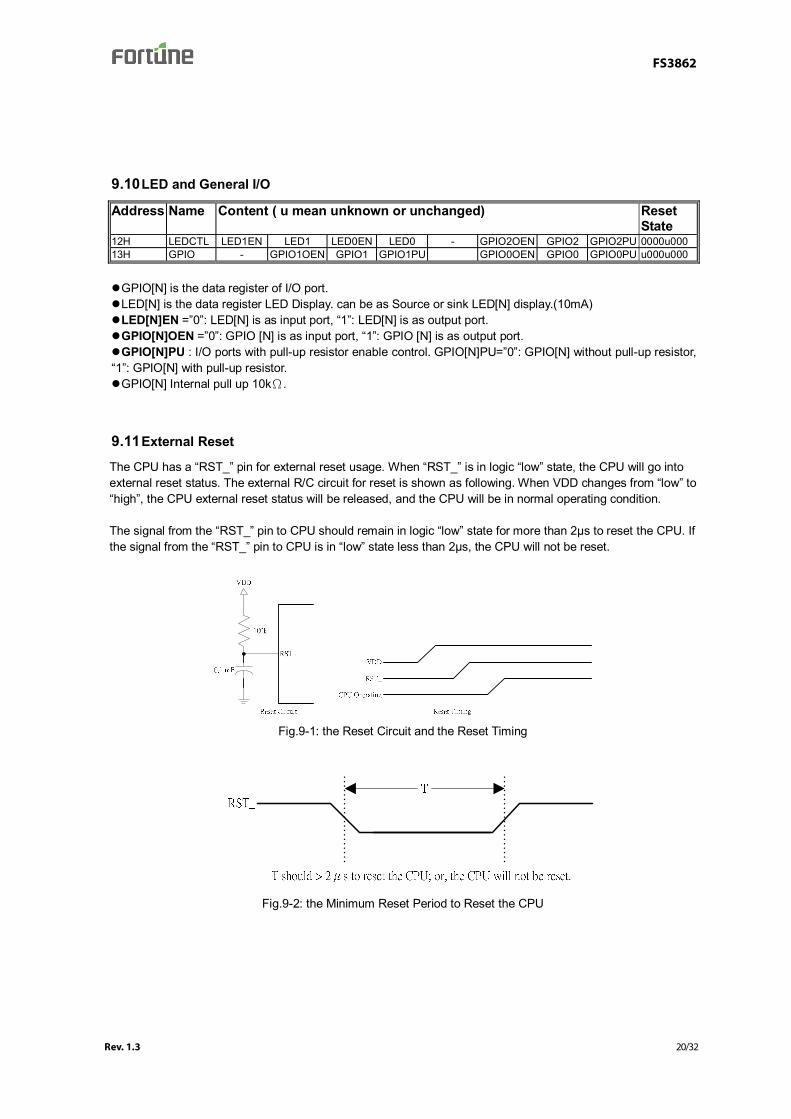
9.11 External Reset
The CPU has a “RST_” pin for external reset usage. When “RST_” is in logic “low” state, the CPU will go into external reset status. The external R/C circuit for reset is shown as following. When VDD changes from “low” to “high”, the CPU external reset status will be released, and the CPU will be in normal operating condition. The signal from the “RST_” pin to CPU should remain in logic “low” state for more than 2µs to reset the CPU. If the signal from the “RST_” pin to CPU is in “low” state less than 2µs, the CPU will not be reset.
Fig.9-1: the Reset Circuit and the Reset Timing
Fig.9-2: the Minimum Reset Period to Reset the CPU
Rev. 1.3 20/32

FS3862
10. Calibration
FS3862 provides a regular resource with 1% accuracy, which to put the calibrating vale into the Peripheral special registers (15H) of Data Memory Structure in IC. They would be burned into ICs during producing. In order to running the calibrating value before the program is running, the Start up /Reset Vector in Program Memory of FS3862 is set to 0000h. Therefore, please add up the following codes during programming:
ORG 0
MOVLW 0ffh
MOVWF 15h
11. Halt and Sleep Modes
FS3862 supports low power working mode. When the user want FS3862 to do nothing and just stand by, FS3862 could be set to Halt mode or Sleep mode to reduce the power consumption by stopping the CPU core working. The two modes will be described below.
11.1 Halt Mode
After CPU executes a Halt command, CPU Program Counter (PC) stops counting until an interrupt command is issued. To avoid program errors caused by Interrupt Return, it is suggested to add a NOP command after Halt to guarantee the program’s normal execution when turning back.
11.2 Sleep Mode After CPU executes Sleep command, all oscillators stop working until an external interrupt command is issued or the CPU is reset. To avoid program errors caused by Interrupt return, it is suggested to add a NOP command after Sleep to guarantee the program’s normal execution. The sleep mode power consumption is about 25uA.
To make sure that CPU consumes minimum power in Sleep mode, it is necessary to close all power blocks and analog circuits before issuing the Sleep command, and make sure that all I/O Ports are in VDD or VSS voltage levels.
It is recommended that users execute the following program before issuing the Sleep command:
MOVLW 080h MOVWF POWER ; Power is off. CLRF GENIO ; Pull up resistor is disconnected and assigned to be input ports. CLRF LEDCTL ; Pull up resistor is disconnected and assigned to be input ports. CLRF CCCTL ; Current regulation reference current is off. CLRF CVCTL ; Voltage regulation reference current is off. CLRF INTF ; Clear the interrupt flags. MOVLW 082h MOVWF INTE ; Enable the external interrupt. SLEEP ; Set the FS3862 into Sleep mode. NOP ; Guarantee that the program works normally when CPU wakes up.
12. Instruction Set
The FS3862 instruction set consists of 37 instructions. Each instruction is a 16-bit word with an OPCODE and one or more operands. The detailed descriptions are shown as below.
Rev. 1.3 21/32
FS3862
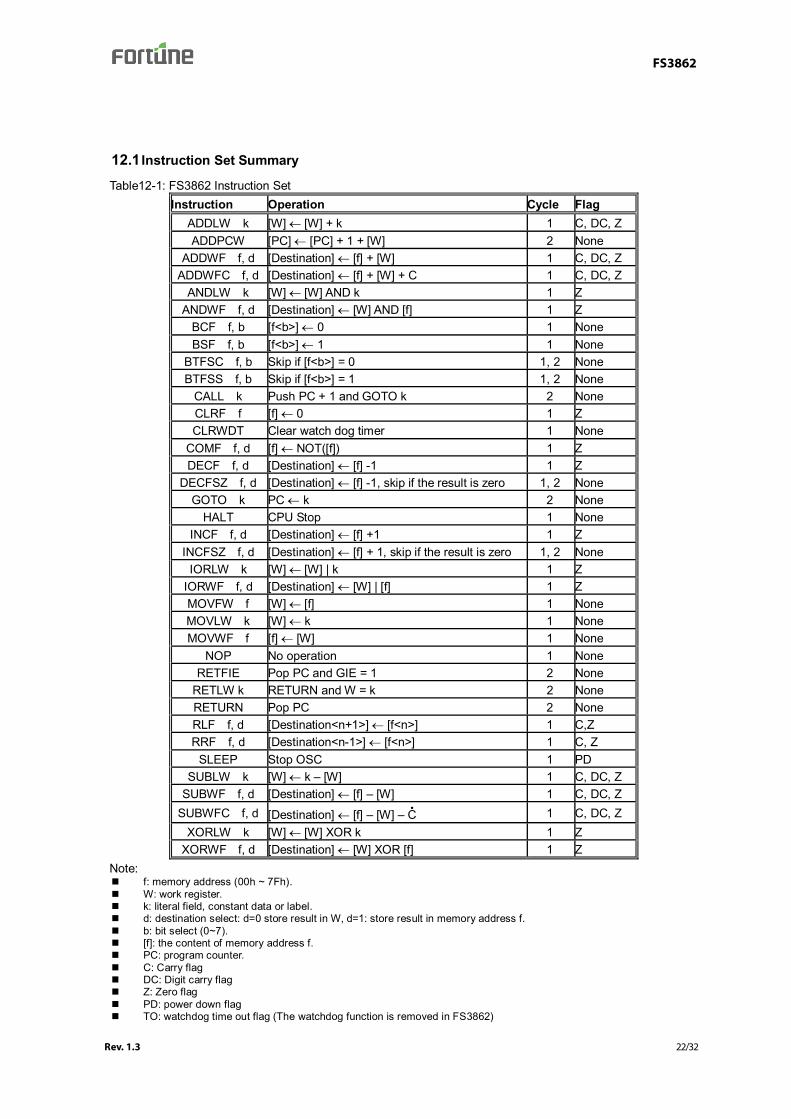
12.1 Instruction Set Summary
Table12-1: FS3862 Instruction Set Instruction Operation Cycle Flag
ADDLW k [W] ← [W] + k 1 C, DC, Z ADDPCW [PC] ← [PC] + 1 + [W] 2 None
ADDWF f, d [Destination] ← [f] + [W] 1 C, DC, Z ADDWFC f, d [Destination] ← [f] + [W] + C 1 C, DC, Z
ANDLW k [W] ← [W] AND k 1 Z ANDWF f, d [Destination] ← [W] AND [f] 1 Z
BCF f, b [f<b>] ← 0 1 None BSF f, b [f<b>] ← 1 1 None
BTFSC f, b Skip if [f<b>] = 0 1, 2 None BTFSS f, b Skip if [f<b>] = 1 1, 2 None
CALL k Push PC + 1 and GOTO k 2 None CLRF f [f] ← 0 1 Z CLRWDT Clear watch dog timer 1 None
COMF f, d [f] ← NOT([f]) 1 Z DECF f, d [Destination] ← [f] -1 1 Z
DECFSZ f, d [Destination] ← [f] -1, skip if the result is zero 1, 2 None GOTO k PC ← k 2 None
HALT CPU Stop 1 None INCF f, d [Destination] ← [f] +1 1 Z
INCFSZ f, d [Destination] ← [f] + 1, skip if the result is zero 1, 2 None IORLW k [W] ← [W] | k 1 Z
IORWF f, d [Destination] ← [W] | [f] 1 Z MOVFW f [W] ← [f] 1 None MOVLW k [W] ← k 1 None MOVWF f [f] ← [W] 1 None
NOP No operation 1 None RETFIE Pop PC and GIE = 1 2 None
RETLW k RETURN and W = k 2 None RETURN Pop PC 2 None RLF f, d [Destination<n+1>] ← [f<n>] 1 C,Z RRF f, d [Destination<n-1>] ← [f<n>] 1 C, Z
SLEEP Stop OSC 1 PD SUBLW k [W] ← k – [W] 1 C, DC, Z
SUBWF f, d [Destination] ← [f] – [W] 1 C, DC, Z SUBWFC f, d [Destination] ← [f] – [W] – C• 1 C, DC, Z
XORLW k [W] ← [W] XOR k 1 Z XORWF f, d [Destination] ← [W] XOR [f] 1 Z
Note: f: memory address (00h ~ 7Fh). W: work register. k: literal field, constant data or label. d: destination select: d=0 store result in W, d=1: store result in memory address f. b: bit select (0~7). [f]: the content of memory address f. PC: program counter. C: Carry flag DC: Digit carry flag Z: Zero flag PD: power down flag TO: watchdog time out flag (The watchdog function is removed in FS3862)
Rev. 1.3 22/32
FS3862
12.2 Struction Description
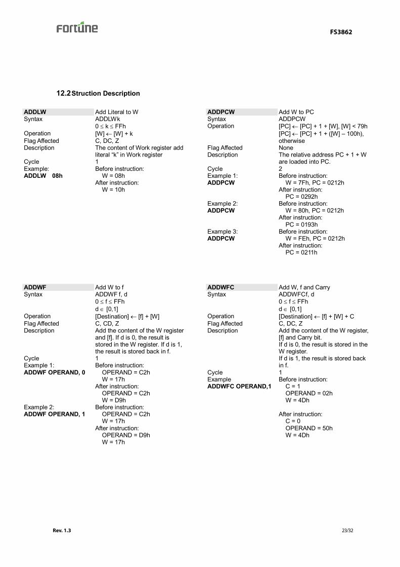
ADDLW Add Literal to W Syntax ADDLW k
0 ≤ k ≤ FFh Operation [W] ← [W] + k Flag Affected C, DC, Z Description The content of Work register add
literal “k” in Work register Cycle 1 Example: ADDLW 08h
Before instruction: W = 08h
After instruction: W = 10h
ADDPCW Add W to PC Syntax ADDPCW Operation [PC] ← [PC] + 1 + [W], [W] < 79h
[PC] ← [PC] + 1 + ([W] – 100h), otherwise
Flag Affected None Description The relative address PC + 1 + W
are loaded into PC. Cycle 2 Example 1: ADDPCW
Before instruction: W = 7Fh, PC = 0212h
After instruction: PC = 0292h
Example 2: ADDPCW
Before instruction: W = 80h, PC = 0212h
After instruction: PC = 0193h
Example 3: ADDPCW
Before instruction: W = FEh, PC = 0212h
After instruction: PC = 0211h
ADDWF Add W to f Syntax ADDWF f, d
0 ≤ f ≤ FFh d ∈ [0,1]
Operation [Destination] ← [f] + [W] Flag Affected C, CD, Z Description Add the content of the W register
and [f]. If d is 0, the result is stored in the W register. If d is 1, the result is stored back in f.
Cycle 1 Example 1: ADDWF OPERAND, 0
Before instruction: OPERAND = C2h W = 17h
After instruction: OPERAND = C2h W = D9h
Example 2: ADDWF OPERAND, 1
Before instruction: OPERAND = C2h W = 17h
After instruction: OPERAND = D9h W = 17h
ADDWFC Add W, f and Carry Syntax ADDWFC f, d
0 ≤ f ≤ FFh d ∈ [0,1]
Operation [Destination] ← [f] + [W] + C Flag Affected C, DC, Z Description Add the content of the W register,
[f] and Carry bit. If d is 0, the result is stored in the W register. If d is 1, the result is stored back in f.
Cycle 1 Example ADDWFC OPERAND,1
Before instruction: C = 1 OPERAND = 02h W = 4Dh
After instruction:
C = 0 OPERAND = 50h W = 4Dh
Rev. 1.3 23/32

FS3862
ANDLW AND literal with W Syntax ANDLW k
0 ≤ k ≤ FFh Operation [W] ← [W] AND k Flag Affected Z Description AND the content of the W register
with the eight-bit literal "k". The result is stored in the W register.
Cycle 1 Example: ANDLW 5Fh
Before instruction: W = A3h
After instruction: W = 03h
ANDWF AND W and f Syntax ANDWF f, d
0 ≤ f ≤ FFh d ∈ [0,1]
Operation [Destination] ← [W] AND [f] Flag Affected Z Description AND the content of the W register
with [f]. If d is 0, the result is stored in the W register. If d is 1, the result is stored back in f.
Cycle 1 Example 1: ANDWF OPERAND,0
Before instruction: W = 0Fh, OPERAND = 88h
After instruction: W = 08h, OPERAND = 88h
Example 2: ANDWF OPERAND,1
Before instruction: W = 0Fh, OPERAND = 88h
After instruction: W = 88h, OPERAND = 08h
BCF Bit Clear f Syntax BCF f, b
0 ≤ f ≤ FFh 0 ≤ b ≤ 7
Operation [f<b>] ← 0 Flag Affected None Description Bit b in [f] is reset to 0. Cycle 1 Example: BCF FLAG, 2
Before instruction: FLAG = 8Dh
After instruction: FLAG = 89h
BSF Bit Set f Syntax BSF f, b
0 ≤ f ≤ FFh 0 ≤ b ≤ 7
Operation [f<b>] ← 1 Flag Affected None Description Bit b in [f] is set to 1. Cycle 1 Example: BSF FLAG, 2
Before instruction: FLAG = 89h
After instruction: FLAG = 8Dh
BTFSC Bit Test skip if Clear Syntax BTFSC f, b
0 ≤ f ≤ FFh 0 ≤ b ≤ 7
Operation Skip if [f<b>] = 0 Flag Affected None Description If bit 'b' in [f] is 0, the next fetched
instruction is discarded and a NOP is executed instead of making it a two-cycle instruction.
Cycle 1, 2 Example: Node BTFSC FLAG, 2 OP1 : OP2 :
Before instruction: PC = address (Node)
After instruction: If FLAG<2> = 0 PC = address(OP2) If FLAG<2> = 1 PC = address(OP1)
BTFSS Bit Test skip if Set Syntax BTFSS f, b
0 ≤ f ≤ FFh 0 ≤ b ≤ 7
Operation Skip if [f<b>] = 1 Flag Affected None Description If bit 'b' in [f] is 1, the next fetched
instruction is discarded and a NOP is executed instead of making it a two-cycle instruction.
Cycle 1, 2 Example: Node BTFSS FLAG, 2OP1 : OP2 :
Before instruction: PC = address (Node)
After instruction: If FLAG<2> = 0 PC = address(OP1) If FLAG<2> = 1 PC = address(OP2)
Rev. 1.3 24/32
FS3862
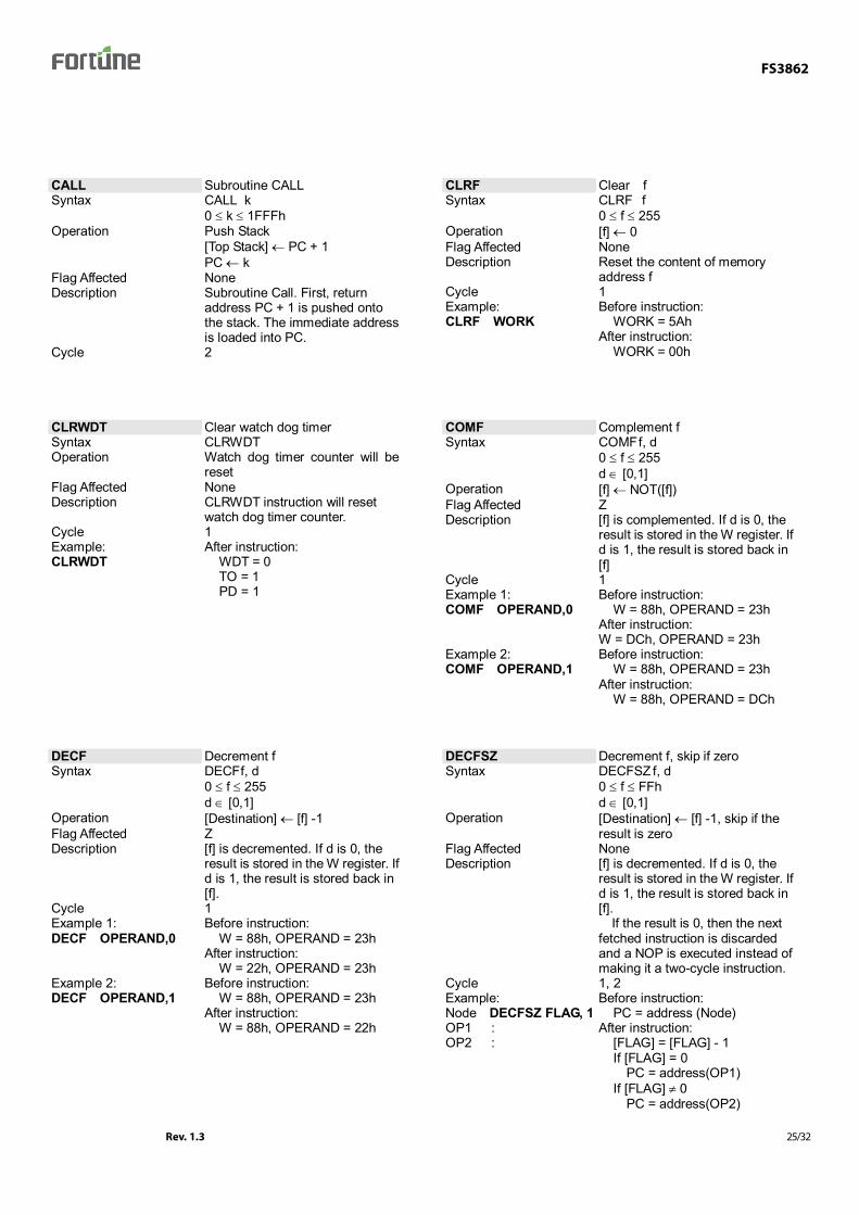
CALL Subroutine CALL Syntax CALL k
0 ≤ k ≤ 1FFFh Operation Push Stack
[Top Stack] ← PC + 1 PC ← k
Flag Affected None Description Subroutine Call. First, return
address PC + 1 is pushed onto the stack. The immediate address is loaded into PC.
Cycle 2
CLRF Clear f Syntax CLRF f
0 ≤ f ≤ 255 Operation [f] ← 0 Flag Affected None Description Reset the content of memory
address f Cycle 1 Example: CLRF WORK
Before instruction: WORK = 5Ah
After instruction: WORK = 00h
CLRWDT Clear watch dog timer Syntax CLRWDT Operation Watch dog timer counter will be
reset Flag Affected None Description CLRWDT instruction will reset
watch dog timer counter. Cycle 1 Example: CLRWDT
After instruction: WDT = 0 TO = 1 PD = 1
COMF Complement f Syntax COMF f, d
0 ≤ f ≤ 255 d ∈ [0,1]
Operation [f] ← NOT([f]) Flag Affected Z Description [f] is complemented. If d is 0, the
result is stored in the W register. If d is 1, the result is stored back in [f]
Cycle 1 Example 1: COMF OPERAND,0
Before instruction: W = 88h, OPERAND = 23h
After instruction: W = DCh, OPERAND = 23h
Example 2: COMF OPERAND,1
Before instruction: W = 88h, OPERAND = 23h
After instruction: W = 88h, OPERAND = DCh
DECF Decrement f Syntax DECF f, d
0 ≤ f ≤ 255 d ∈ [0,1]
Operation [Destination] ← [f] -1 Flag Affected Z Description [f] is decremented. If d is 0, the
result is stored in the W register. If d is 1, the result is stored back in [f].
Cycle 1 Example 1: DECF OPERAND,0
Before instruction: W = 88h, OPERAND = 23h
After instruction: W = 22h, OPERAND = 23h
Example 2: DECF OPERAND,1
Before instruction: W = 88h, OPERAND = 23h
After instruction: W = 88h, OPERAND = 22h
DECFSZ Decrement f, skip if zero Syntax DECFSZ f, d
0 ≤ f ≤ FFh d ∈ [0,1]
Operation [Destination] ← [f] -1, skip if the result is zero
Flag Affected None Description [f] is decremented. If d is 0, the
result is stored in the W register. If d is 1, the result is stored back in [f]. If the result is 0, then the next fetched instruction is discarded and a NOP is executed instead of making it a two-cycle instruction.
Cycle 1, 2 Example: Node DECFSZ FLAG, 1OP1 : OP2 :
Before instruction: PC = address (Node)
After instruction: [FLAG] = [FLAG] - 1 If [FLAG] = 0 PC = address(OP1) If [FLAG] ≠ 0 PC = address(OP2)
Rev. 1.3 25/32
FS3862
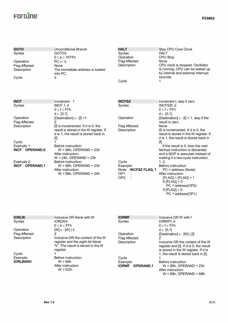
GOTO Unconditional Branch Syntax GOTO k
0 ≤ k ≤ 1FFFh Operation PC ← k Flag Affected None Description The immediate address is loaded
into PC. Cycle 2
HALT Stop CPU Core Clock Syntax HALT Operation CPU Stop Flag Affected None Description CPU clock is stopped. Oscillator
is running. CPU can be waked up by internal and external interrupt sources.
Cycle 1
INCF Increment f Syntax INCF f, d
0 ≤ f ≤ FFh d ∈ [0,1]
Operation [Destination] ← [f] +1 Flag Affected Z Description [f] is incremented. If d is 0, the
result is stored in the W register. If d is 1, the result is stored back in [f].
Cycle 1 Example 1: INCF OPERAND,0
Before instruction: W = 88h, OPERAND = 23h
After instruction: W = 24h, OPERAND = 23h
Example 2: INCF OPERAND,1
Before instruction: W = 88h, OPERAND = 23h
After instruction: W = 88h, OPERAND = 24h
INCFSZ Increment f, skip if zero Syntax INCFSZf, d
0 ≤ f ≤ FFh d ∈ [0,1]
Operation [Destination] ← [f] + 1, skip if the result is zero
Flag Affected None Description [f] is incremented. If d is 0, the
result is stored in the W register. If d is 1, the result is stored back in [f]. If the result is 0, then the next fetched instruction is discarded and a NOP is executed instead of making it a two-cycle instruction.
Cycle 1, 2 Example: Node INCFSZ FLAG, 1OP1 : OP2 :
Before instruction: PC = address (Node)
After instruction: [FLAG] = [FLAG] + 1 If [FLAG] = 0 PC = address(OP2) If [FLAG] ≠ 0 PC = address(OP1)
IORLW Inclusive OR literal with W Syntax IORLW k
0 ≤ k ≤ FFh Operation [W] ← [W] | k Flag Affected Z Description Inclusive OR the content of the W
register and the eight-bit literal "k". The result is stored in the W register.
Cycle 1 Example: IORLW 85H
Before instruction: W = 69h
After instruction: W = EDh
IORWF Inclusive OR W with f Syntax IORWF f, d
0 ≤ f ≤ FFh d ∈ [0,1]
Operation [Destination] ← [W] | [f] Flag Affected Z Description Inclusive OR the content of the W
register and [f]. If d is 0, the result is stored in the W register. If d is 1, the result is stored back in [f].
Cycle 1 Example: IORWF OPERAND,1
Before instruction: W = 88h, OPERAND = 23h
After instruction: W = 88h, OPERAND = ABh
Rev. 1.3 26/32

FS3862
MOVFW Move f to W Syntax MOVFW f
0 ≤ f ≤ FFh Operation [W] ← [f] Flag Affected None Description Move data from [f] to the W
register. Cycle 1 Example: MOVFW OPERAND
Before instruction: W = 88h, OPERAND = 23h
After instruction: W = 23h, OPERAND = 23h
MOVLW Move literal to W Syntax MOVLW k
0 ≤ k ≤ FFh Operation [W] ← k Flag Affected None Description Move the eight-bit literal "k" to the
content of the W register. Cycle 1 Example: MOVLW 23H
Before instruction: W = 88h
After instruction: W = 23h
MOVWF Move W to f Syntax MOVWF f
0 ≤ f ≤ FFh Operation [f] ← [W] Flag Affected None Description Move data from the W register to
[f]. Cycle 1 Example: MOVWF OPERAND
Before instruction: W = 88h, OPERAND = 23h
After instruction: W = 88h, OPERAND = 88h
NOP
No Operation Syntax NOP Operation No Operation Flag Affected None Description No operation. NOP is used for
one instruction cycle delay. Cycle 1
RETFIE Return from Interrupt Syntax RETFIE Operation [Top Stack] => PC
Pop Stack 1 => GIE
Flag Affected None Description The program counter is loaded
from the top stack, then pop stack. Setting the GIE bit enables interrupts.
Cycle 2
RETLW Return and move literal to W Syntax RETLW k
0 ≤ k ≤ FFh Operation [W] ← k
[Top Stack] => PC Pop Stack
Flag Affected None Description Move the eight-bit literal "k" to the
content of the W register. The program counter is loaded from the top stack, then pop stack.
Rev. 1.3 27/32
FS3862
Return Return from Subroutine Syntax RETURN Operation [Top Stack] => PC
Pop Stack Flag Affected None Description The program counter is loaded
from the top stack, then pop stack.
Cycle 2
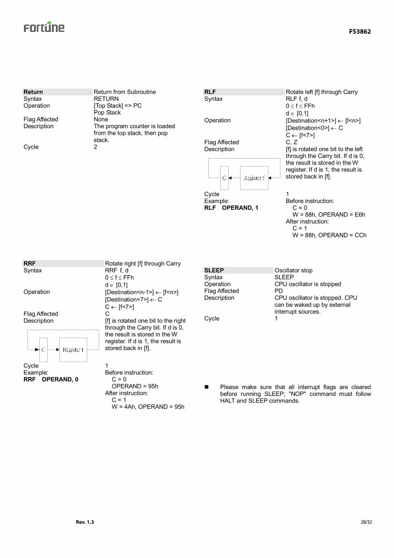
RLF Rotate left [f] through Carry Syntax RLF f, d
0 ≤ f ≤ FFh d ∈ [0,1]
Operation
[Destination<n+1>] ← [f<n>] [Destination<0>] ← C C ← [f<7>]
Flag Affected C, Z Description
[f] is rotated one bit to the left through the Carry bit. If d is 0, the result is stored in the W register. If d is 1, the result is stored back in [f].
Cycle 1 Example: RLF OPERAND, 1
Before instruction: C = 0 W = 88h, OPERAND = E6h
After instruction: C = 1 W = 88h, OPERAND = CCh
RRF Rotate right [f] through Carry Syntax RRF f, d
0 ≤ f ≤ FFh d ∈ [0,1]
Operation [Destination<n-1>] ← [f<n>] [Destination<7>] ← C C ← [f<7>]
Flag Affected C Description
[f] is rotated one bit to the right through the Carry bit. If d is 0, the result is stored in the W register. If d is 1, the result is stored back in [f].
Cycle 1 Example: RRF OPERAND, 0
Before instruction: C = 0 OPERAND = 95h
After instruction: C = 1 W = 4Ah, OPERAND = 95h
SLEEP Oscillator stop Syntax SLEEP Operation CPU oscillator is stopped Flag Affected PD Description CPU oscillator is stopped. CPU
can be waked up by external interrupt sources.
Cycle 1
Please make sure that all interrupt flags are cleared before running SLEEP; "NOP" command must follow HALT and SLEEP commands.
Rev. 1.3 28/32
FS3862
SUBLW Subtract W from literal Syntax SUBLW k
0 ≤ k ≤ FFh Operation [W] ← k – [W] Flag Affected C, DC, Z Description Subtract the content of the W
register from the eight-bit literal "k". The result is stored in the W register.
Cycle 1 Example 1: SUBLW 02H
Before instruction: W = 01h
After instruction: W = 01h C = 1 Z = 0
Example 2: SUBLW 02H
Before instruction: W = 02h
After instruction: W = 00h C = 1 Z = 1
Example 3: SUBLW 02H
Before instruction: W = 03h
After instruction: W = FFh C = 0 Z = 0
SUBWF Subtract W from f Syntax SUBWFf, d
0 ≤ f ≤ FFh d ∈ [0,1]
Operation [Destination] ← [f] – [W] Flag Affected C, DC, Z Description Subtract the content of the W
register from [f]. If d is 0, the result is stored in the W register. If d is 1, the result is stored back in [f],
Cycle 1 Example 1: SUBWF OPERAND, 1
Before instruction: OPERAND = 33h, W = 01h
After instruction: OPERAND = 32h C = 1 Z = 0
Example 2: SUBWF OPERAND, 1
Before instruction: OPERAND = 01h, W = 01h
After instruction: OPERAND = 00h C = 1 Z = 1
Example 3: SUBWF OPERAND, 1
Before instruction: OPERAND = 04h, W = 05h
After instruction: OPERAND = FFh C = 0 Z = 0
SUBWFC Subtract W and Carry from f Syntax SUBWFC f, d
0 ≤ f ≤ FFh d ∈ [0,1]
Operation [Destination] ← [f] – [W] –C• Flag Affected C, DC, Z Description Subtract the content of the W
register from [f]. If d is 0, the result is stored in the W register. If d is 1, the result is stored back in [f].
Cycle 1 Example 1: SUBWFC OPERAND, 1
Before instruction: OPERAND = 33h, W = 01h C = 1
After instruction: OPERAND = 32h, C = 1, Z = 0
Example 2: SUBWFC OPERAND, 1
Before instruction: OPERAND = 02h, W = 01h C = 0
After instruction: OPERAND = 00h, C = 1, Z = 1
Example 3: SUBWFC OPERAND, 1
Before instruction: OPERAND = 04h, W = 05h C = 0
After instruction: OPERAND = FEh, C = 0, Z = 0
XORWF Exclusive OR W and f Syntax XORWF f, d
0 ≤ f ≤ FFh d ∈ [0,1]
Operation [Destination] ← [W] XOR [f] Flag Affected Z Description Exclusive OR the content of the
W register and [f]. If d is 0, the result is stored in the W register. If d is 1, the result is stored back in [f].
Cycle 1 Example: XORWF OPERAND, 1
Before instruction: OPERAND = 5Fh, W = ACh
After instruction: OPERAND = F3h
Rev. 1.3 29/32
FS3862
XORLW Exclusive OR literal with W Syntax XORLWk
0 ≤ k ≤ FFh Operation [W] ← [W] XOR k Flag Affected Z Description Exclusive OR the content of the
W register and the eight-bit literal "k". The result is stored in the W register.
Cycle 1 Example: XORLW 5Fh
Before instruction: W = ACh
After instruction: W = F3h
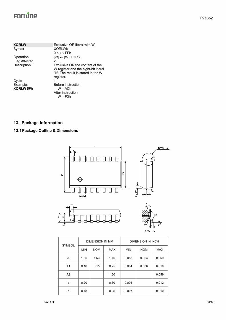
13. Package Information
13.1 Package Outline & Dimensions
DIMENSION IN MM DIMENSION IN INCH SYMBOL
MIN NOM MAX MIN NOM MAX
A 1.35 1.63 1.75 0.053 0.064 0.069
A1 0.10 0.15 0.25 0.004 0.006 0.010
A2 1.50 0.059
b 0.20 0.30 0.008 0.012
c 0.18 0.25 0.007 0.010
Rev. 1.3 30/32

FS3862
e 0.635 BASIC 0.025 BASIC
D 4.80 4.90 5.00 0.189 0.193 0.197
E 5.79 5.99 6.20 0.228 0.236 0.244
E1 3.81 3.91 3.99 0.150 0.154 0.157
L 0.41 0.635 1.27 0.016 0.025 0.050
h 0.25 0.50 0.010 0.020
L1 0.254 BASIC 0.010 BASIC
ZD 0.229 REF 0.009 REF
R1 0.20 0.33 0.008 0.013
R 0.20 0.008
θ 0 ゚ 8 ゚ 0 ゚ 8 ゚
θ1 0 ゚ 8 ゚ 0 ゚ 8 ゚
θ2 5 ゚ 10 ゚ 15 ゚ 5 ゚ 10 ゚ 15 ゚
JEDEC MO-137(AB)
Notes: Dimension D does not include mold protrusions or gate burrs.
Mold protrusions and gate burrs shall not exceed 0.06 inch per side.
Rev. 1.3 31/32

FS3862
14. Revision History
Version Date Page Description 1.3 2007/05 3 ~ 32 Revise all chapters
Rev. 1.3 32/32


![[Tugas Materi] IC Datasheet](https://static.fdocuments.net/doc/165x107/55cf9680550346d0338be37c/tugas-materi-ic-datasheet.jpg)