Data Sheet - Department of Physics |cms/cfeb/datasheets/hdmp1032.pdfAgilent HDMP-1032/1034...
32
Agilent HDMP-1032/1034 Transmitter/Receiver Chip Set Data Sheet Features • 3.3 V supply, low power dissipation 590 mW Tx, 660 mW Rx • On-chip encode/decode using Conditional Inversion Master Transition (CIMT) protocol • 1:N broadcast ready configurable receiver inputs allow multi-point data broadcast using a single transmitter • Parallel Automatic Synchronization System (PASS) allows receiver to read recovered words with local reference clock • Robust simplex mode • Wide range serial rate 260-1400 MBaud (user selectable) • 5 V tolerant TTL interface 16 or 17 Bits wide • Low cost 64 pin plastic package 14x14 mm 2 PQFP Applications • Cellular base station • ATM switch • Backplane/bus extender • Video, image acquisition • Point to point data link • Implement SCI-FI standard Description The HDMP-1032 transmitter and HDMP-1034 receiver are used together to build a high-speed data link for point-to-point communication. These silicon bipolar transmitter and receiver chips are housed in standard plastic 64 pin PQFP packages. From the user’s viewpoint, these products can be thought of as a “virtual ribbon cable” interface for the transmission of data and con- trol words. A parallel word loaded into the Tx (transmitter) chip is delivered to the Rx (receiver) chip over a serial channel and is then reconstructed into its origi- nal parallel form. The channel can be either a coaxial copper cable or optical link The chip set hides from the user the complexity of encoding, multiplexing, clock extraction, demultiplexing and decoding. The CIMT encoding scheme used en- sures the DC balance of the serial line. When data or control words are not being sent the transmitter sends idle words. The serial data rate of the Tx/Rx link is selectable in three ranges and extends from 208 to 1120 Mbit/s. This translates into an encoded serial rate of 260 to 1400 MBaud. The parallel data interface is 16 bit TTL. A flag bit is also present and can be used as an extra 17th bit under the user’s control. This bit can be used as an even or odd word indicator for dual-word transmission. The encoding of the flag bit can be scrambled to reduce the probabil- ity of erroneous word alignment. A user control space is also provided. If TXCNTL is asserted on the Tx chip, the least signifi- cant 14 bits of the data will be sent and the RXCNTL line on the Rx chip will indicate the data is a Control Word. At the Rx, the PASS feature allows the recovered words to be clocked out with the local 1.4 GBd Transmitter/Receiver Chip Set with CIMT Encoder/Decoder and Variable Data Rate.
-
Upload
nguyenthuan -
Category
Documents
-
view
215 -
download
0
Transcript of Data Sheet - Department of Physics |cms/cfeb/datasheets/hdmp1032.pdfAgilent HDMP-1032/1034...

Agilent HDMP-1032/1034Transmitter/ReceiverChip SetData Sheet
Features• 3.3 V supply, low power
dissipation590 mW Tx, 660 mW Rx
• On-chip encode/decode usingConditional Inversion MasterTransition (CIMT) protocol
• 1:N broadcast readyconfigurable receiver inputs allowmulti-point data broadcast using asingle transmitter
• Parallel AutomaticSynchronization System (PASS)allows receiver to read recoveredwords with local reference clock
• Robust simplex mode• Wide range serial rate
260-1400 MBaud (user selectable)• 5 V tolerant TTL interface
16 or 17 Bits wide• Low cost 64 pin plastic package
14x14 mm2 PQFP
Applications• Cellular base station• ATM switch• Backplane/bus extender• Video, image acquisition• Point to point data link• Implement SCI-FI standard
DescriptionThe HDMP-1032 transmitter andHDMP-1034 receiver are usedtogether to build a high-speeddata link for point-to-pointcommunication. These siliconbipolar transmitter and receiverchips are housed in standardplastic 64 pin PQFP packages.
From the user’s viewpoint, theseproducts can be thought of as a“virtual ribbon cable” interface forthe transmission of data and con-trol words. A parallel word loadedinto the Tx (transmitter) chip isdelivered to the Rx (receiver)chip over a serial channel and isthen reconstructed into its origi-nal parallel form. The channelcan be either a coaxial coppercable or optical link
The chip set hides from theuser the complexity of encoding,multiplexing, clock extraction,demultiplexing and decoding. TheCIMT encoding scheme used en-sures the DC balance of the serialline. When data or control words
are not being sent the transmittersends idle words.
The serial data rate of the Tx/Rxlink is selectable in three rangesand extends from 208 to 1120Mbit/s. This translates into anencoded serial rate of 260 to1400 MBaud. The parallel datainterface is 16 bit TTL. A flag bitis also present and can be used asan extra 17th bit under the user’scontrol. This bit can be used asan even or odd word indicatorfor dual-word transmission. Theencoding of the flag bit can bescrambled to reduce the probabil-ity of erroneous word alignment.
A user control space is alsoprovided. If TXCNTL is assertedon the Tx chip, the least signifi-cant 14 bits of the data will besent and the RXCNTL line on theRx chip will indicate the data isa Control Word.
At the Rx, the PASS featureallows the recovered words tobe clocked out with the local
1.4 GBd Transmitter/Receiver Chip Set withCIMT Encoder/Decoder and Variable Data Rate.
2
REFCLK. This feature is particu-larly useful when the Tx clockand REFCLK are synchronous.The PASS system also supportssynchronization of multiplechannels.
The chipset is compatible withprevious versions of the G-Linkchipset (HDMP-10x2/10x4) pro-vided the latter are used in 16 bitSimplex with Periodic Sync Pulseor External Reference OscillatorMode (Simplex Method II or III).
Table of Contents
Topic Page
Typical Applications ................................................................................................... 3Setting the Operating Data Rate Range .................................................................. 4Transmitter Block Diagram ....................................................................................... 5Receiver Block Diagram ............................................................................................ 6Parallel Automatic Synchronization System .......................................................... 7Transmitter Timing .................................................................................................... 10Receiver Timing ........................................................................................................... 11DC Electrical Specifications ..................................................................................... 12AC Electrical Specifications ..................................................................................... 12TXCLK and REFCLK Requirements ........................................................................... 13Absolute Maximum Ratings ...................................................................................... 13Thermal Characteristics ............................................................................................ 14I/O Type Definitions .................................................................................................... 14Pin-Out Diagrams ........................................................................................................ 15Transmitter Pin Definitions ........................................................................................ 16Receiver Pin Definitions ............................................................................................ 18Mechanical Dimensions ............................................................................................ 21
Appendix: Internal Architecture Information
Line Code Description ................................................................................................ 22Data, Control, and Idle Word Codes ........................................................................ 22Tx Operation Principles – Encoding & Phase Lock Loop .................................... 24Rx Operation Principles – Decoding & Phase Lock Loop.................................... 25Integrator Capacitor & Power SupplyBypassing/Grounding ................................................................................................. 26TTL and High Speed I/O ............................................................................................. 26Data Bus Line/Broadcast Transmission ................................................................. 27Nomenclature Changes betweenHDMP-1032/34 and HDMP-1022/24 .......................................................................... 30Pin Cross Reference Table ........................................................................................ 31

3
Typical ApplicationsThe HDMP-1032/1034 chipsetwas designed for ease of useand flexibility. The customer cantailor the use of this productthrough the configuration of thelink based on specific system re-quirements and application needs.Typical applications range frombackplane serialization and busextension to cellular base stations.
All modes are built up from thebasic simplex transmission modeas shown in Figure 1a.
For digital video transmission,simplex links are common. TheHDMP-1032/1034 chipset cantransmit 16 bits of parallel datain standard or broadcast simplexmode (Figures 1a, 1b).
If the bus is 32 bits wide, theHDMP-1032/1034 chipset is ca-pable of sending this data word astwo separate word segments withthe use of an external mux anddemux as shown in Figure 1c. Inthis mode, the transmitter andreceiver use the FLAG bit to indi-cate the first or second wordsegment. The HDMP-1032/1034chipset may also be configuredin full duplex to achieve a 32 bitwide bus extension. In addition,32 bit wide data can be transmit-ted over two parallel serial linesas shown in Figure 1d.
Low latency bus extension ofa 16 bit wide data bus may beachieved using the full duplexconfiguration (Figure 1e). In thismode, link startup is achievedby exchange of control words.
Figure 1. Various configurations using the HDMP-1032/1034.
Tx RxTXCLK RXCLK0/1
A) 16 BIT SIMPLEX TRANSMISSION
REFCLK
TXCLKTx Rx RXCLK0/1
B) 16 BIT BROADCAST TRANSMISSION
Rx RXCLK0/1
Rx RXCLK0/1
REFCLK
REFCLK
REFCLK
TXCLKTx Rx RXCLK0/1MUX DEMUX
C) 32 BIT SIMPLEX TRANSMISSION
REFCLK
TXCLKTx Rx RXCLK0/1
TXCLKTx Rx RXCLK0/1
D) 32 BIT SIMPLEX TRANSMISSION
REFCLK
REFCLK
TXCLKTx Rx RXCLK0/1
RXCLK0/1 Rx TxTXCLK
E) 16 BIT DUPLEX TRANSMISSION
REFCLK
REFCLK

4
HDMP-1032 (Tx), HDMP-1034 (Rx)Typical Operating Rates1,2
Tc = –20°C to +85°C, VCC = 3.15V to 3.45V
Parallel Word Rate Serial Data Rate Serial Baud Rate(MWord/sec) (MBits/sec) (MBaud)
DIV1 DIV0 Range Range Range
0 0 40 70 (max) 640 1120 (max) 800 1400 (max)
0 1 20 45 320 720 400 900
1 0 13 (min) 26 208 (min) 416 260 (min) 520
Figure 2. Typical data rates showing ranges of operation1.
Notes:1. All values in this table and graph are typical unless otherwise noted by (min) or (max), (min) indicates a minimum guaranteed value,(max) indicates a maximum guaranteed value.2. All values in this table are expected for a BER less than 10-14.
0/0
0/1
1/0
5 25 50 75 100
200015001000500100
800
400
260 (MIN.) 520
900
1400 (MAX.)
DIV
1 /
DIV
0
SERIAL BAUD RATE (MBaud)
WORD RATE (MWords/sec)
is unique. The user serial datarate is calculated as:
The baud rate includes an addi-tional four encoding bits (20 bitstotal) that the HDMP-1032/34G-Link chipset transmits. Theserial baud rate is calculated as:
Example 2 (Overlapping Ranges)Some applications may have aparallel word rate that seemsto fit in two ranges of opera-tion. For example, a 42.5 MHz(42.5 MWord/s) parallel datarate falls within two ranges:DIV1/0 = (0/0) and DIV1/0 =(0/1). According to the table, asetting of DIV1/0 = (0/1) gives
Serial Baud Rate =
(–––––) (–––––) =
1200 MBaud
20bitsWord
60MWsec
Serial Data Rate =
(–––––) (–––––) =
960 MBits/sec
16bitsWord
60MWsec
Setting the Operating Data Rate RangeThe HDMP-1032/1034 chipsetcan operate from 260 MBaud to1400 MBaud. It is divided intothree operating data ranges witheach range selected by settingDIV1/0 as shown in the TypicalOperating Rates table. Twoexamples have been provided inorder to help in understandingand using this table.
Example 1 (Unique Range)It is desired to transmit a 16 bitparallel word operating at a fre-quency of 60 MHz (60 MWord/sec). Both the Tx and Rx mustbe set to a range that covers thisword rate. According to the tableonly a setting of DIV1/0 = (0/0)allows a parallel input word rateof 40 to 70 MHz. This rangesetting easily accommodates therequired 60 MHz word rate and
an upper rate of 45 MHz while asetting of DIV1/0 = (0/0) gives alower rate of 40 MHz. The upperand lower data rates stated in thetables are typical values unlessindicated by (min) or (max) andmay vary between individual parts.However, each transmitter/receiverhas overlapping ranges of opera-tion providing continuous bandcoverage from 260 to 1400 MBaud.
In this example, each transmitter/receiver will permit a 42.5 MHzparallel data rate but it is sug-gested that DIV0 be tied to ajumper that can be set either tologic ‘1’ (open allowing DIV0 tofloat high) or logic ‘0’ (ground).This allows the design to accom-modate both ranges for maximumflexibility. This technique is rec-ommended whenever operatingnear the upper and lower ends oftwo adjacent word rate ranges.

5
Figure 3. HDMP-1032 Transmitter Block Diagram.
The C-Field logic, based on theinputs at TXCNTL, TXDATA,TXFLGENB and TXFLAG, sup-plies the four bits of the C-fieldto the encoded word mux. Thesebits contain information regard-ing the word type: Control, Dataor Idle. In order for the TXFLAGbit to be used as an additionaldata bit, TXFLGENB must be sethigh on the Tx and RXFLGENBmust be set high on the Rx. Ifscrambling of the encoding of theflag bit is desired, ESMPXENB pinmust be set high on both the Txand Rx. See Flag Descramblersection on next page for a moredetailed description of theenhanced simplex mode.
The W-Field logic (word field)presents either bits TX[0-15]or an Idle Word to the encodedword mux.
Encoded Word MuxThe Word Mux accepts the fourencoding bits from the C-Fieldand 16 data bits from theW-Field. These 20 bits of parallelinformation are then multiplexedto a serial line based on theinternal high-speed serial clock.
HDMP-1032 Tx Block DiagramThe HDMP-1032 transmitter wasdesigned to accept 16 bit wideparallel words and transmit themover a high-speed serial line. TheHDMP-1032 performs the follow-ing functions:• Latching parallel word input• Phase lock to TXCLK• High speed clock multiplication• Word encoding• Parallel to Serial Multiplexing
PLL/Clock GeneratorThe Phase Lock Loop and ClockGenerator are responsible forgenerating all the internal clocksneeded by the transmitter toperform its functions. Theseclocks are based on a suppliedword clock (TXCLK) and controlsignals (TXDIV1/0, TCLKENB).TXCLK is the incoming wordclock. The PLL/Clock Generatorlocks on to this incomingrate and multiplies the wordrate clock by 20 (16 word bits+ 4 encoding bits). As lock isachieved, LOCKED is set high.The TXDIV1/0 pins configure thetransmitter to accept incomingdata words within the desiredfrequency range.
By setting TCLKENB high, theuser may provide an externalTTL high speed serial clock atTXCLK. This clock replaces theinternal VCO clock and is in-tended for diagnostic purposesonly. This uncharacterized signalis used directly by the high-speedserial circuitry to output the se-rial data at speeds that are notwithin the VCO range.
C-Field and W-FieldEncoder LogicThis logic determines what infor-mation is sent to the encodedword mux. If TXCNTL is high, thelogic sends bits TX[0-13] and aC-Field (coding field) encodedas a control word regardless ofthe state of TXDATA. If TXCNTLis low and TXDATA is high,the logic sends TX[0-15] and aC-Field encoded as a data word.If neither TXCNTL nor TXDATAis set high, then the transmitterassumes the link is not beingused. In this case, the logic sub-mits an Idle Word to the encodedword mux to maintain the DCbalance on the serial link andallow the receiver to maintainfrequency and phase lock.
C-FIELD ENCODER
TXFLAG
TX[0-15]W-FIELD
ENCODER
INVERT
WORD MUX
TX
FLG
EN
B
ES
MP
XE
NB
TX
CLK
TX
DIV
1/0
TC
LKE
NB
LOC
KE
D
PLL / CLOCK GENERATOR
AC
CU
MU
LAT
E
TXCAP0
TXCAP1
HSOUT
FLAG ENCODER
TXDATA
TXCNTL LAT
CH
IN
PU
TIN
PU
T
LAT
CH
SIGN
+

6
SignThe sign circuitry determines thedisparity of the encoded word.Disparity is defined as the totalnumber of high bits minus thetotal number of low bits.
Accumulator BlockThis block is responsible forkeeping track of total disparityof all previously sent words.
Invert BlockThe Invert block is responsiblefor maintaining the DC balanceof the serial line. It determinesbased on history and the signof the current encoded wordwhether the current encodedword should be inverted tobring the serial line closer tothe desired 50% duty cycle.
HDMP-1034 Rx Block DiagramThe HDMP-1034 receiver wasdesigned to convert a serial datasignal sent from the HDMP-1032
into either 16 or 17 bit wideparallel data. The HDMP-1034performs the following functions:• Frequency Lock• Phase Lock• Encoded Word Synchronization• De-multiplexing• Word Decoding• Encoding Error Detection
Input Sampler and Clock-DataRecovery (CDR)In order to compensate for anyamplitude distortion present inthe serial data signal, the high-speed inputs, HSIN± , are alwaysequalized. The CDR block locksto the frequency of the REFCLKand to the phase of the sampledinput signal. The recovereddata is sent to the DEMUX blockand a bit-rate clock is sent tothe Clock Generator block. Ifthe serial data signal is absent,the CDR block will maintainfrequency lock onto REFCLK.
Figure 4. HDMP-1034 Receiver Block Diagram.
The RXDIV1/0 pins select thedata rate range by dividing theVCO range by 1, 2 or 4. WhenRXDIV1/0 = 1/1, the internalVCO is bypassed and the testclock input TSTCLK can beused as the serial input.
Clock GeneratorUsing the recovered bit-rateclock, the CLOCK GENERATORblock generates all of the re-quired internal clocks includingthe word rate clocks: RXCLK0/1.
Using the WORD ALIGN block’sbit adjust output, the phase ofthe word-rate clocks is adjustedbit by bit for proper word align-ment. For testing purposesthis adjustment function can bedisabled using the WSYNCDSBinput; word alignment can alsobe forced using the #RESET pin.
RXREADY
WORD ALIGN SYNC
LOGIC
RXERROR
RXDATA
RXCNTL
SHFOUT
SRQOUT
RXDSLIP
OU
TP
UT
LA
TC
H
DE
LAY
RXFLAG
RX[0-15]
SHFIN
SRQIN
PASSENB
INVERT
DECODE
FLAG DESCRM
HSIN
RX
FLG
EN
B
ES
MP
XE
NB
CLOCK GENERATOR
DEMUXCDR
RXCLK0/1
#RE
SE
T
WS
YN
CD
SB
REFCLK
RX
DIV
1/0
PASS SYSTEM
RXCAP1/0TS
TC
LK
+

7
When the Tx and Rx clock arenot synchronous, FIFO’s are usu-ally used to cross the frequencydomains. The size of the FIFOand the frequency differencedetermine the maximum packetsize of transmission.
When the clock from the Tx issynchronous with the Rx clock,data can be transmitted continu-ously without FIFO’s since theparallel output data is synchro-nous with the local REFCLK.However, due to link distance andother physical variables, the rela-tive phase of the REFCLK to therecovered data is unpredictable.Because of this unknown phase,the sampling of the recoveredword must be adjusted so that theinternal setup/hold times are notviolated. Furthermore, in a multi-channel system, the setting of thephase must be consistent so thattime slots across the channelsare preserved.
The PASS system was designed toaddress these issues by sensingthe phase difference between thelocal REFCLK with the recoveredclock, and shifts the phase ofthe parallel output data with theDELAY block, such that it can beclocked out with the rising edge
static valid code-field bits beingembedded within the data-field.
Enhanced simplex mode can beturned off (ESMPXENB=0) tomake it compatible withprevious versions of G-Link.With this mode turned off andTXFLGENB=1, the flag bit issent unscrambled to the Rx.If TXFLGENB=0, the flagbit will alternate at the Tx.When RXFLGENB=0, the Rxwill use this alternating flag forerror checking.
Parallel Automatic SynchronizationSystem (Pass)As shown in Figure 4, this systemconsists of three blocks: theparallel delay block (DELAY),the output latch block (OUTPUTLATCH), and the synchronizationlogic block (SYNC LOGIC). Thissystem was designed to providea simple interface to the paralleloutputs for a synchronous system.
BackgroundTraditionally, the parallel outputsare clocked out with the fallingedge of RXCLK1 as shown inFigure 4.1. Since this clock isrecovered from the serial data,this clock is synchronous withthe remote clock at the Tx.
Demultiplexer (DEMUX)This block takes the recoveredserial data from the CDR blockand demultiplexes it into a 20-bitparallel word comprised of a16-bit word-field and 4-bitcode-field.
Decoder (DECODE)This block decodes the 4-bitcode-field and determineswhether the 16-bit word-field is:normal or inverted; data, control,or idle words; or errors. Theflag bit is also decoded fromthe data word.
Word Alignment (WORD ALIGN)This block detects the error out-put of the decoder block. Upondetecting two consecutive errors,WORD ALIGN requests a bitadjustment to the clock generator(assuming WSYNCDSB=0).
If enhanced simplex mode isengaged (ESMPXENB=1), theWord Align block looks for atransition in the scrambled flagbit over a window of 32 words.If a transition is not detected,WORD ALIGN requests a bitadjustment to the clock generator(assuming WSYNCDSB=0).
When the bit adjustment outputhas been low for 64 up to 128words, the RXREADY output goeshigh. If the bit adjustment outputgoes high, RXREADYimmediately goes low.
Flag Descrambler(FLAG DESCRM)This block descrambles the flagbit if the enhanced simplex modeis engaged (ESMPXENB=1); oth-erwise, the flag bit is unaltered.Scrambling ensures that the flagbit is dynamic and thus can bedetected by the word alignmentblock. Scrambling of the flagbit provides an extra level ofprotection to guard against im-proper word alignment caused by Figure 4.1. Traditional G-Link configuration with PASS disabled (PASSENB=0).
Recovered data words and RXCLK0/1 are synchronous with TXCLK.
HSOUT± HSIN±RxTx
TXCLK
TXCLK
REFCLK
REFCLKSRQOUT
NC
NC
SRQIN SHFINSHFOUT
RXCLK0/1RX[0-15]
NCNC
DATA 16 BITS TX[0-15]
PASSENB

8
of the REFCLK. By adjusting thephase of the data word ratherthan REFCLK, the optimal setuptime is achieved for the inputlatches of the chip interfacing tothe Rx.
As the relative phase between theHSIN± input and the REFCLKdrift slowly over time due to envi-ronmental variations, the PASSsystem is able to absorb this tosome degree, and is able to resetand re-optimize the samplingwhen the margin is exceeded.
DELAY BlockThe parallel DELAY block has anadjustable delay range of 20% to80% of the data word. Its delayis controlled by the SYNC LOGICblock. This delay block is usedfor all of the data bits, flag bit,as well as the status bits.
OUTPUT LATCH BlockThis block is a bank of positiveedge triggered D-flip/flops. Theclock is selected by the SYNCLOGIC block to be either the re-covered clock RXCLK1 when thePASS system is disabled, or theREFCLK when the PASS systemis enabled (PASSENB=1).
SYNC LOGIC BlockThe SYNC LOGIC block’s func-tion is to compare the phase ofthe recovered data to REFCLK, toset the state of the DELAY block,to detect when the DELAY rangehas been exceeded, and to re-cover with a new DELAY setting.It is also designed to support amaster/slave configuration in amulti-channel environment.
When RXREADY goes high, theoptimal delay choice is deter-mined at the shift outputSHFOUT:SHFOUT = 0 DELAY retractSHFOUT = 1 DELAY extend
The actual setting of the DELAYblock is determined with the shiftinput SHFIN.
When the phase of the REFCLKdrifts to within 10% of the wordboundary, the RXDSLIP outputis set high, and a new choice ofSHFOUT is chosen. The shift re-quest output SQROUT is set highwhen a RXDSLIP condition isdetected, or if the shift requestinput SRQIN goes high.
Figure 4.2. Single channel configuration with PASS enabled (PASSENB=1).Recovered data words and RXCLK0/1 are synchronous with REFCLK.
HSOUT± HSIN±RxTx
TXCLK
REFCLK
REFCLKSRQOUT
NC
SRQIN SHFINSHFOUT
RXCLK0/1RX[0-15]DATA 16 BITS TX[0-15]
PASSENB
+VCC
Single Channel ConfigurationIn a single channel configuration,SHFIN is simply tied to SHFOUTas shown in Figure 4.2. The daisychaining signal SRQIN is set low(grounded) and SRQOUT is leftunconnected.
After RXREADY goes high, theDELAY block can absorb a phasevariation between the serial inputHSIN± and the REFCLK a mini-mum of ideally ± 4 serial bits,or 20% of the word period. Thismargin is reduced due to finiterise/fall times and setup timesof the internal circuitry.

9
a shift request (SRQOUT=1) isissued which propagates to themaster. The master again selectsan optimum SHFOUT, which setsthe DELAY blocks of all receiversconsistently.
The phase absorption margin fora multiple channel configurationis the same as the single channelcase, less the channel-to-channelskews.
Figure 4.3. Multiple channel configuration with PASS Enabled (PASSENB=1).
Multiple Channel ConfigurationThe connections for a multiplechannel configuration are shownin Figure 4.3. The daisy-chainsignals SRQIN and SRQOUT areused to allow each receiver’s PASSsystem shift requests to propagateto the master, which is the last ofthe chain. The master then con-trols the shift command SHFOUT,which is tied common to theSHFIN of each receiver. The first
SRQIN in the chain is grounded;the SRQOUT of the master aswell as the SHFOUT outputs ofthe slave units are left uncon-nected.
When the internal parallel databoundary of the master, or anyof the slaves come within 10% ofthe REFCLK, the RXDSLIP outputis set high by the respective Rx,
HSOUT– HSIN–Rx
(SLAVE)Tx
TXCLK REFCLKSRQOUT
SRQIN SHFINSHFOUT
RXCLK0/1RX[0-15]DATA 16 BITS TX[0-15]
PASSENB
+VCC
HSOUT– HSIN–Tx
TXCLK REFCLKSRQOUT
SRQIN SHFINSHFOUT
RXCLK0/1RX[0-15]DATA 16 BITS TX[0-15]
PASSENB
+VCC
HSOUT– HSIN–Tx
TXCLK
REFCLK
REFCLKSRQOUT
NC
SRQIN SHFINSHFOUT
RXCLK0/1RX[0-15]DATA 16 BITS TX[0-15]
PASSENB
+VCC
Rx (SLAVE)
Rx (MASTER)
NC
NC

10
Figure 5. HDMP-1032 (Tx) Timing Diagram.
HDMP-1032 (Tx) Timing CharacteristicsTc = –20°C to +85°C, VCC = 3.15V to 3.45V
Symbol Parameter Unit Min. Typ. Max.
ts Setup Time, for TX[0-15], TXDATA, TXCNTL and nsec 2.5TXFLAG Relative to Rising Edge of TXCLK.
th Hold Time, for TX[0-15], TXDATA, TXCNTL and nsec 2.5TXFLAG Relative to Rising Edge of TXCLK.
HDMP-1032 (Tx) TimingThe Tx timing diagram is shownin Figure 5. Under normal opera-tions, the Tx PLL locks an inter-nally generated clock to theincoming TXCLK at which timeLOCKED is set high. The incom-ing data, TX[0-15], TXDATA,TXCNTL, and TXFLAG arelatched by this internal clock. Thedata must be valid for tsbefore it is sampled and remainvalid for a time th after it issampled.
The setup and hold time param-eters, ts and th, are referenced tothe rising edge of TXCLK.
The start of a word, bit TX[0],in the high speed serial outputoccurs after a delay of td afterthe rising edge of the TXCLK.The typical value of td isapproximately one clock cycle.
ts th
td
W-FIELDC-FIELD
TXCLK
TX[0-15] TXDATA TXCNTL TXFLAG
HSOUT

11
Figure 6. HDMP-1034 (Rx) Timing Diagram.
HDMP-1034 (Rx) Timing CharacteristicsTc = –20°C to +85°C, VCC = 3.15V to 3.45V. Typical values are at Tc = 25°C, VCC = 3.3V
Symbol Parameter Unit Min. Typ. Max.
td Synchronous Output Delay referenced to the falling nsec 0 2.0 3.5edge of RXCLK1, PASS System Disabled (PASSENB=0).
tdp Synchronous Output Delay referenced to the rising nsec 6.0 6.6 8.0edge of REFCLK, PASS System Enabled (PASSENB=1).
tsk Allowable skew between HSIN and REFCLK before nsec 20% wordPASS system resets, PASSENB=1. period
-0.4 nsec
HDMP-1034 (Rx) TimingThe Rx timing diagram whenRXREADY=1 is shown in Figure6. The serial data stream isdeserialized into a parallel wordat 1/20 the serial baud rate.
When the PASS system is dis-abled (PASSENB=0), there is alatency delay of two words fromthe input of the first serial bit of aword to the parallel outputs. Theparallel outputs, RX[0-15],RXFLAG, RXREADY, RXERROR,
RXDATA, RXCNTL and RXDSLIPare clocked out with the fallingedge of RXCLK1 and appear aftera delay of td. RXCLK1 and itscomplement RXCLK0 are both50% duty cycle clocks.
When the PASS system is enabled(PASSENB=1), the timing of theparallel word is adjusted auto-matically ± 30% of the word pe-riod so that it can be clocked outwith the rising edge of REFCLKand appear after a delay of tdp.
CWORD 1
W CWORD 2
W CWORD 3
W CWORD 4
W
HSIN
RXCLK1
RXCLK0
REFCLK
tdp
td
RX[0]
BIT 0
NOTE: W = 16 BIT WORD FIELD, C = 4 BIT CODE FIELD
12
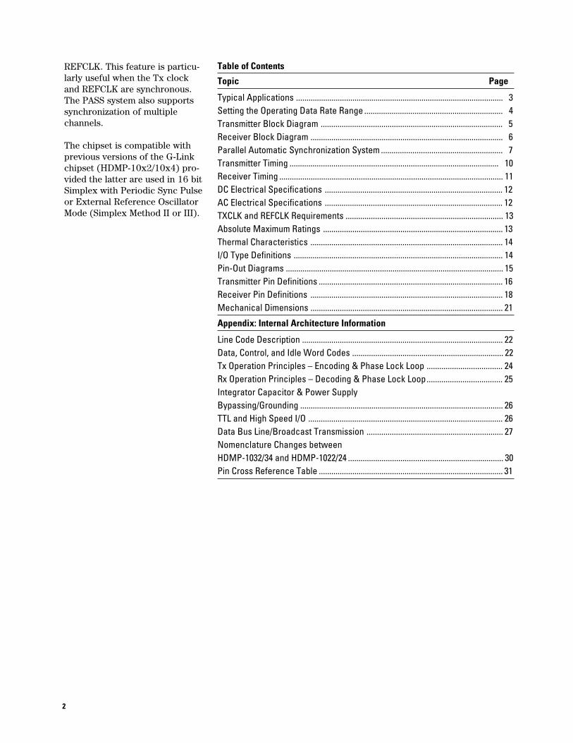
HDMP-1032 (Tx), HDMP-1034 (Rx)DC Electrical SpecificationsTc = –20°C to +85°C, VCC = 3.15V to 3.45V, Typical values are at Tc = 25°C, VCC = 3.3V
Symbol Parameter Unit Min. Typ. Max.
VIH,TTL TTL Input High Voltage Level, Guaranteed high signal V 2.0 VCCfor all inputs.
VIL,TTL TTL Input Low Voltage Level, Guaranteed low signal V 0 0.8for all inputs.
VOH,TTL TTL Output High Voltage Level, IOH = -400 µA V 2.2 VCC
VOL,TTL TTL Output Low Voltage Level, IOL = 500 µA V 0 0.6
IIH,TTL Input High Current, VIN = VCC µA 40
IIL,TTL Input Low Current, VIN = 0 volts µA 600
VIP,H50 H50 Input Peak-To-Peak Differential Voltage mV 200
VOP,BLL BLL Output Peak-To-Peak Differential Voltage, mV 1000Terminated with 50 Ω, ac coupled
ICC,Tx Transmitter VCC Supply Current mA 180
ICC,Rx Receiver VCC Supply Current mA 200
AC Electrical SpecificationsTc = 25°C
Symbol Parameter Unit Min. Typ. Max.
tr,TTL in Input TTL Rise Time, 0.8 to 2.0 volts nsec 2
tf,TTL in Input TTL Fall Time, 2.0 to 0.8 volts nsec 2
tr,TTL out Output TTL Rise time, 0.8 to 2.0 volts, 10 pF load nsec 3.0
tf,TTL out Output TTL Fall Time, 2.0 to 0.8 volts, 10 pF load nsec 3.0
tr,BLL BLL Rise Time, Terminated with 50, ac coupled1 psec 240
tf,BLL BLL Fall Time, Terminated with 50, ac coupled1 psec 240
VSWRi,H50 H50 Input VSWR 2:1
VSWRo,BLL BLL Output VSWR 2:1
tfa Transmitter & Receiver Frequency Acquisition Time msec 4at Power-on2
tRx_wa Receiver Word Alignment Time Words 300
Notes1. Rise and fall times are measured between 20% and 80% of the voltage range.2. Frequency acquisition time is independent of DIV1/DIV0 data rate range.

13
LatencyTc = 25°C
Latency Latency Definition (Word Clock Cycles)
PASSENB = 0 PASSENB = 1
Tx 1.4 1.4 Delay from the rising edge of TXCLK to the first bit TX[0]in the serial stream
Rx 2.6 3.0 Delay from the first bit RX[0] in the serial stream to thefalling edge of RXCLK1 (or the rising edge of REFCLK ifthe PASS system is enabled, PASSENB=1)
Link 4.0 4.4
Transmit Word Clock (TXCLK) and Receiver Reference Clock (REFCLK) RequirementsTc = –20°C to +85°C, VCC = 3.15 V to 3.45 V
Symbol Parameter Unit Min. Typ. Max.
Ftol TXCLK and REFCLK Frequency Tolerance ppm -100 +100(REFCLK is referenced to TXCLK)
Symm Symmetry (Duty Cycle) % 40 60
HDMP-1032 (Tx), HDMP-1034 (Rx)Absolute Maximum RatingsTA = 25°C except as specified. Operation in excess of any one of these conditions may result in permanent damage tothe device.
Symbol Parameter Unit Min. Max.
VCC Supply Voltage V -0.5 5.0
VIN,TTL TTL Input Voltage V -0.7 5.5
VIN,BLL H50 Input Voltage V 2.0 VCC
IO,TTL TTL Output Source Current mA 13
Tstg Storage Temperature °C -65 +150
TJ Junction Temperature °C 0 +150
Tmax Maximum Assembly Temperature (10 seconds maximum) °C +260

14
HDMP-1032 (Tx) Thermal CharacteristicsTA = 25°C
Symbol Parameter Unit Typ.
θjc1 Thermal Resistance, Die to Case °C/W 8
PD Power Dissipation, VCC = 3.3 V mW 590
HDMP-1034 (Rx) Thermal CharacteristicsTA = 25°C
Symbol Parameter Unit Typ.
θjc1 Thermal Resistance, Die to Case °C/W 8
PD Power Dissipation, VCC = 3.3 V mW 660
Note:1. Based on independent package testing by HP. θjc for the HDMP-1032 and HDMP-1034 is 50°C/W. θjc is measured on a standard3" x 3" two layer PCB in a still air environment. In order to determine the actual junction temperature in a given application, use the followingformula: TJ = TC + (θjc x PD), where TC is the case temperature measured on the top center of the package and PD is the power being dissipated.
I/O Type Definitions
I/O Type Definition
I-TTL Input TTL. Floats high when left open.
O-TTL Output TTL
HS_OUT 50 Ω Matched Output Driver. Will drive AC coupled 50 Ω loads. All unused outputsshould be AC coupled to a 50 Ω resistor to ground.
HS IN High Speed Input
C Filter Capacitor Node
S Power Supply or Ground

15
Figure 7. HDMP-1032 (Tx) Package Layout, Top View.
Figure 8. HDMP-1034 (Rx) Package Layout, Top View.
A HDMP-1032 LOT# Tx DATE CODE
GND 1TX[14] 2TX[15] 3
TXCNTL 4TXDATA 5TXFLAG 6
NC 7VCC_TTL 8
GND_TTL 9TXFLGENB 10
ESMPXENB 11LOCKED 12
VCC 13GND 14
NC 15NC 16
48 GND47 TX[1]46 TX[0]45 NC44 NC43 NC42 NC41 VCC_TTL40 GND_TTL39 NC38 NC37 TXCLK36 VCC35 GND34 NC33 TXCAP1
VC
C_H
S 1
7G
ND
_HS
18
HS
OU
T–
19
HS
OU
T+
20
NC
21
NC
22
NC
23
VC
C 2
4G
ND
25
TX
DIV
0 2
6T
XD
IV1
27
TC
LKE
NB
28
NC
29
GN
D_A
1 3
0V
CC
_A1
31
TX
CA
P0
32
64 V
CC
63 T
X[1
3]62
TX
[12]
61 T
X[1
1]60
TX
[10]
59 T
X[9
]58
TX
[8]
57 V
CC
_A2
56 G
ND
_A2
55 T
X[7
]54
TX
[6]
53 T
X[5
]52
TX
[4]
51 T
X[3
]50
TX
[2]
49 V
CC
A HDMP-1034 LOT# Rx DATE CODE
GND_TTL 1RX[1] 2RX[0] 3
RXREADY 4RXERROR 5RXDSLIP 6VCC_TTL 7
GND_TTL 8VCC 9
GND 10REFCLK 11TSTCLK 12
SHFIN 13SHFOUT 14SRQOUT 15VCC_HS 16
48 GND_TTL47 RX[14]46 RX[15]45 RXFLAG44 RXDATA43 RXCNTL42 VCC_TTL41 GND_TTL40 VCC39 GND38 RXCLK137 RXCLK036 WSYNCDSB35 #RESET34 SRQIN33 RXCAP1
GN
D_H
S 1
7H
SIN
+ 1
8H
SIN
– 1
9G
ND
_HS
20
NC
21
RX
FLG
EN
B 2
2E
SM
PX
EN
B 2
3V
CC
24
GN
D 2
5P
AS
SE
NB
26
NC
27
RX
DIV
0 2
8R
XD
IV1
29
VC
C_A
30
GN
D_A
31
RX
CA
P0
32
64 V
CC
_TT
L63
RX
[2]
62 R
X[3
]61
RX
[4]
60 R
X[5
]59
RX
[6]
58 R
X[7
]57
VC
C_T
TL
56 G
ND
55 R
X[8
]54
RX
[9]
53 R
X[1
0]52
RX
[11]
51 R
X[1
2]50
RX
[13]
49 V
CC
_TT
L
16
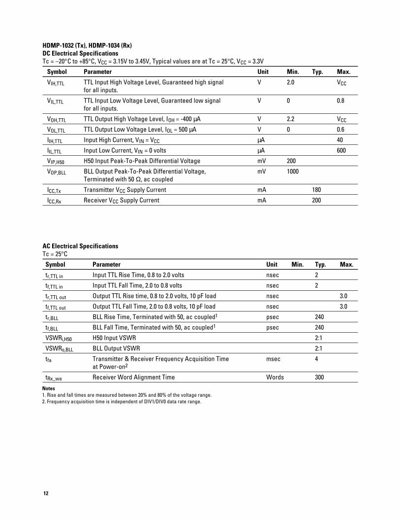
HDMP-1032 (Tx) Pin Definition
User Mode Options
Name Pin Type Signal
TXFLGENB 10 I-TTL Flag Bit Mode Select: When this input is high, the TXFLAG bitinput is sent as an extra 17th data bit during data word transfers.As an example, the flag bit can be used as an even or odd wordindicator for 32 bit transmission. The RXFLGENB input on the Rxchip must be set to the same value as the TXFLGENB pin.
ESMPXENB 11 I-TTL Enhanced Simplex Mode Enable: Enables scrambling of the FlagBit encoding. The ESMPXENB pin on the Rx chip must be set tothe same value. This mode should be enabled unless compatibilitywith previous versions of G-Link (i.e. HDMP-1024/1014) is desireddesired which don’t have this feature.
TXDATA 5 I-TTL Transmit Data Word: This input tells the chip that the user hasvalid data to be transmitted. When this pin is asserted andTXCNTL is low, bits TX[0-15] and optionally TXFLAG are encodedand sent as a data word.
TXCNTL 4 I-TTL Transmit Control Word: This input tells the Tx chip that the useris requesting a control word to be transmitted. When this pin isasserted, bits TX[0-13] are sent as a control word. If TXCNTL andTXDATA are asserted simultaneously, TXCNTL takes precedence.Idle words are transmitted if both TXDATA and TXCNTL are low.
High-Speed Serial/Parallel I/O
HSOUT+ 20 HS_OUT Serial Data Output: These pins form a buffer line logic driver,HSOUT- 19 which is a 50 Ω terminated PECL compatible output.
TX[0] 46 I-TTL Word Inputs: When sending data words, TX[0-15] are serialized.TX[1] 47 When sending control words, TX[0-13] are serialized.TX[2] 50TX[3] 51TX[4] 52TX[5] 53TX[6] 54TX[7] 55TX[8] 58TX[9] 59TX[10] 60TX[11] 61TX[12] 62TX[13] 63TX[14] 2TX[15] 3
TXFLAG 6 I-TTL Flag Bit: When TXFLGENB is active, this input is sent as an extradata bit in addition to the 16 data word bits. When TXFLGENB isnot asserted, this input is ignored and an alternating internal flagbit is transmitted to allow the Rx chip to perform error detectionduring data word transfers. The Flag Bit is not sent when a controlword is transmitted.

17
HDMP-1032 (Tx) Pin Definition (continued)
PLL/Clock Generator
Name Pin Type Signal
TXCAP0 32 C Loop Filter Capacitor: A 0.1 µF min. loop filter capacitor, C2, mustTXCAP1 33 be connected across TXCAP0 and TXCAP1 for all combinations of
TXDIV1/TXDIV0. See Figure 12.
TXCLK 37 I-TTL Transmit Word Clock Input: When TCLKENB is low, this word rateclock input is phase locked and multiplied to generate the high-speed serial clock. When TCLKENB is high, the PLL is bypassedand TXCLK becomes the serial clock.
TXDIV0 26 I-TTL VCO Divider Select: These pins program the VCO divider chain toTXDIV1 27 operate at full, half or quarter speed. See Typical Operating Rates
table and Figure 2.
LOCKED 12 O-TTL Locked to TXCLK: This pin goes high when the transmit PLLachieves frequency lock to the TXCLK signal.
Power Supply/Ground
VCC 13 S Logic Power Supply: Normally 3.3 volts. This power supply is24 used for the internal transmitter logic.364964
VCC_TTL 8 S TTL Power Supply: Normally 3.3 volts. Used for all TTL transmitter41 input and output buffer cells.
VCC_HS 17 S Serial Output Power Supply: Normally 3.3 volts. Used for SerialOutput pins.
VCC_A1 31 S Analog Power Supply: Normally 3.3 volts. Used for the analogVCC_A2 57 section.GND 1 S Ground: Normally 0 volts. Tie to ground.
14253548
GND_TTL 9 S TTL Ground: Normally 0 volts. Tie to ground.40
GND_HS 18 S Serial Output Ground: Normally 0 volts.
GND_A1 30 S Analog Ground: Normally 0 volts.GND_A2 56
Test Mode/No Connect Pins
TCLKENB 28 I-TTL Enable External Serial Rate Clock Input: When set high, this inputcauses the TXCLK input to be used for the serial transmit clockrather than the internal VCO clock. It is intended for diagnosticpurposes and normally tied low.
NC 7 No Connect: These pins should be left unconnected.15162122232934383942434445

18
HDMP-1034 (Rx) Pin Definition
User Mode Options/Status
Name Pin Type Signal
RXFLGENB 22 I-TTL Flag Bit Mode Select: When set high, the RXFLAG bit output isavailable to the user as an extra 17th data bit.
ESMPXENB 23 I-TTL Enhanced Simplex Mode Enable: Enables descrambling of the FlagBit encoding. The ESMPXENB pin on the Tx chip must be set to thesame value. This mode should be enabled unless compatibility withprevious versions of G-Link (i.e. HDMP-1022/1012) is desired whichdon’t have this feature.
PASSENB 26 I-TTL Enable Parallel Automatic Synchronization System: The parallelRx data and control words are read out with REFCLK insteadof the incoming word’s parallel clock. The relative phase of theparallel output bits is internally adjusted so that they are clockedout with the rising edge of the REFCLK.
RXDATA 44 O-TTL Data Word Available Output: This output indicates that the Rxchip word outputs RX[0-15] have a data word.
RXCNTL 43 O-TTL Control Word Available Output: This output indicates that the Rxchip word outputs RX[0-13] have a control word.
High-Speed Serial/Parallel I/O
HSIN+ 18 HS_IN Serial Data InputHSIN- 19
RX[0] 3 O-TTL Word OutputsRX[1] 2RX[2] 63RX[3] 62RX[4] 61RX[5] 60RX[6] 59RX[7] 58RX[8] 55RX[9] 54RX[10] 53RX[11] 52RX[12] 51RX[13] 50RX[14] 47RX[15] 46
RXFLAG 45 O-TTL Flag Bit: If both TXFLGENB and RXFLGENB have been asserted,this output indicates the value of the transmitted flag bit whichcan be used as an extra 17th data bit.
Link Status
RXREADY 4 O-TTL Receiver Ready: This signal is asserted when the word alignmentblock has seen error-free code field nibbles for 64 up to 128consecutive words. When ESMPXENB = 1, the toggling of thescrambled flag bit is also checked. RXREADY is de-assertedupon 2 consecutive errors in the code field or if the toggling ofthe flag bit is absent when ESMPXENB=1.
RXERROR 5 O-TTL Received Data Error: Asserted when a word is received whichdoes not correspond to either a valid Data, Control, or IdleWord encoding.

19
HDMP-1034 (Rx) Pin Definition (continued)
CDR/Clock Generator
Name Pin Type Signal
RXCAP0 32 C Loop Filter Capacitor: A 0.1 µF min. loop filter capacitor, C2, mustRXCAP1 33 be connected across RXCAP0 and RXCAP1 for all combinations
of RXDIV1/RXDIV0. See Figure 12.
REFCLK 11 I-TTL Reference Clock Input: The Rx PLL uses this input for frequencylock. In addition, RX[0-15], RXFLAG, RXDATA, RXCNTL, RXREADY,RXERROR, and RXDSLIP are clocked out on the rising edge ofREFCLK when PASSENB=1.
RXDIV0 28 I-TTL VCO Divider Select: These pins program the VCO divider chainRXDIV1 29 to operate at full, half, or quarter speed. See Typical Operating
Rates table and Figure 2.
RXCLK0 37 O-TTL Recovered Word-Rate Clock Outputs: These outputs are the PLLRXCLK1 38 recovered word rate clocks. RX[0-15], RXFLAG, RXDATA,
RXCNTL, RXREADY, RXERROR, and RXDSLIP are clocked out onthe falling edge of RXCLK1 when PASSENB=0. RXCLK0 is theinverse of RXCLK1.
Power Supply/Ground
VCC 9 S Power Supply: Normally 3.3 volts. This power supply is used for24 all the core logic other than the output drivers.40
VCC_TTL 7 S TTL Power Supply: Normally 3.3 volts. Used for all TTL receiver42 input and output buffer cells.495764
VCC_HS 16 S High-Speed Supply: Normally 3.3 volts. This supply is used toprovide clean references for the high-speed inputs, HSIN+and HSIN-.
VCC_A 30 S Analog Power Supply: Normally 3.3 volts. This supply is used tofeed power to the analog section of the chip.
GND 10 S Ground: Normally 0 volts. Tie to ground.253956
GND_TTL 1 S TTL Ground: Normally 0 volts. Tie to ground.84148
GND_HS 17 S High-Speed Input Ground: When tied to ground, the input20 impedance of HSIN+ and HSIN- are each matched to 50 Ω. In
order to obtain high impedance (high-Z) inputs for 1:N broadcastapplications, 18 KΩ series resistors to -5 V are recommended.
GND_A 31 S Analog Ground: Normally 0 volts. This ground is used for theanalog PLL portion of the chip.

20
HDMP-1034 (Rx) Pin Definition (continued)
Pass System
RXDSLIP 6 O-TTL Rx Word Slip: This output is asserted whenever the phase of theparallel word relative to the reference clock has exceeded therange of the internal delay, which results in a slippage of oneword. See discussion of PASS system on page 7.
SHFIN 13 I-TTL Shift Input: This input controls the delay of the parallel bits tobe clocked out by REFCLK when PASSENB=1. In a single Rxconfiguration, SHFIN is connected to SHFOUT. In a multiple Rxconfiguration, all SHFIN are connected to the master’s SHFOUT.
SHFOUT 14 O-TTL Shift Output: This output, normally connected to SHFIN, isgenerated based on the relative phase between REFCLK andthe internal parallel output bits.
SRQIN 34 I-TTL Shift Request Input: In a daisy chain configuration, this inputallows a shift request to be propagated to the master. SRQIN isconnected to the SRQOUT of the previous Rx in a multi-receiverconfiguration.
SRQOUT 15 O-TTL Shift Request Output: In a daisy chain configuration, this outputis connected to the SRQIN input of the next receiver. SRQOUTgoes high when a SRQIN=1 or when the relative phase betweenthe REFCLK and the internal parallel bits requires a shift.
Test Mode/No Connect Pins
TSTCLK 12 I-TTL External Serial Rate Clock Input: When RXDIV1/0 = 1/1, this inputis used in place of the normal VCO signal, effectively disablingthe PLL and allowing the user to provide an external serial clockfor testing. Pin is normally tied to VCC_TTL.
#RESET 35 I-TTL Reset: When this active low input is asserted the word alignmentis reset. Upon release (low to high) the normal word alignmentprocess is reinstated. Pin used for test purposes and is normallytied to VCC_TTL.
WSYNCDSB 36 I-TTL Word Sync Disable: When high, disables resynchronization toword edge upon errors encountered in the C-field of the incomingencoded word. Pin used for test purposes and is normally tied low.
NC 21 No Connect: These pins should be left unconnected.27

21
Package Information
Item Details
Package Material Plastic
Lead Finish Material 85% Tin, 15% Lead
Lead Finish Thickness 300–800 µm
Lead Skew 0.20 mm max
Lead Coplanarity 0.10 mm max(seating plane method)
Mechanical Dimensions of HDMP-1032/34
Dimensional Parameter D1/E1 D/E b e L c G A2 A1 A(in millmeters)
HDMP-103X 14.00 17.20 0.35 0.80 0.88 0.17 0.25 2.00 0.25 2.35Max
Tolerance ±0.10 ±0.25 ±0.05 Basic +0.15/ Max Gage +0.10/ Max-0.10 Plane -0.05
Mechanical Dimensions
PIN #1 ID
EE1
D
D1
e
b
c
A1
A2
L
G
A
HDMP-103x TOP VIEW
12345678910111213141516
48474645444342414039383736353433
64 63 62 61 60 59 58 57 56 55 54 53 52 51 50 49
17 18 19 20 21 22 23 24 25 26 27 28 29 30 31 32

22
Line Code DescriptionThe HDMP-1032/1034 line codeis Conditional Invert Master Tran-sition (CIMT) as illustrated inFigure 9. The CIMT line codeuses three types of words: Datawords, Control words, and Idlewords. Idle words are generatedinternally by the Tx when bothTXDATA and TXCNTL are low.Each word consists of a WordField (W-Field) followed by aCoding Field (C-Field). TheC-Field has a master transition.Users can send arbitrary informa-tion carried by Data or ControlWords. The DC balance of theline code is enforced automati-cally by the Tx. Idle words havea single rising edge at the mastertransition when operating innon-enhanced simplex mode.
The coding definitions are sum-marized in the table on the next
page. Note that the leftmost bit ineach table is the first bit to betransmitted in time, while therightmost bit is the last bit tobe transmitted.
Data Word CodesIn Data Word mode, all 16 bitsof the Tx are transmitted tothe Rx, along with a flag bit. IfTXFLGENB=1, then the usercontrols this bit with TXFLAG;otherwise it is internally set toalternate.
Control Word CodesIn Control Word mode, 14 bits aretransmitted to the Rx. The lower7 bits X0-X6 are sent in thew0-w6 space, and the upper7 bits X7-X13 are sent in thew9-w15 space. Bits w7 and w8are forced 01 for true, and 10for inverted control words. Theshifting of the word field is for
backward compatibility with pre-vious versions of G-Links chip sets.
Idle Word and Error CodesTwo Idle Words, IW1a and IW1bare provided. Unused word codesare mapped into Error States.
Enhanced Simplex ModeIn this mode (ESMPXENB=1),the flag bit is scrambled at theTx and descrambled at the Rx.Since the Rx uses the scrambledflag bit for frame alignment, it isalso defined for Control and IdleWords. However, the flag bit isonly available to the user in theData Word mode. The first bitw0 is also scrambled to aid wordalignment.
Figure 9. HDMP-1032/1034 (Tx/Rx Pair) Line Code.
Appendix: Internal Architecture Information
WORD FIELD
16 BITS
CODING FIELD 4 BITS
IDLE WORD
SERIAL BIT STREAM
WORD K WORD K+1
MASTER TRANSITION
MASTER TRANSITION

23
Coding1 with ESMPXENB=0(Compatible with previous G-Link chips, HDMP-1012/14, HDMP-1022/24)Word Type Flag W-Field C-Field
w0 w1 w2 w3 w4 w5 w6 w7 w8 w9 w10 w11 w12 w13 w14 w15 c0 c1 c2 c3Data Word StructureData = True 0 X0 X1 X2 X3 X4 X5 X6 X7 X8 X9 X10 X11 X12 X13 X14 X15 1 1 0 1Data = Inverted 0 #(X0 X1 X2 X3 X4 X5 X6 X7 X8 X9 X10 x11 X12 X13 X14 X15) 0 0 1 0Data = True 1 X0 X1 X2 X3 X4 X5 X6 X7 X8 X9 X10 X11 X12 X13 X14 X15 1 0 1 1Data = Inverted 1 #(X0 X1 X2 X3 X4 X5 X6 X7 X8 X9 X10 x11 X12 X13 X14 X15) 0 1 0 0Control Word StructureControl = True X0 X1 X2 X3 X4 X5 X6 0 1 X7 X8 X9 X10 X11 X12 X13 0 0 1 1Control = Inverted #(X0 X1 X2 X3 X4 X5 X6) 1 0 #(X7 X8 X9 X10 X11 X12 X13) 1 1 0 0Idle Word StructureIdle Word 1a 1 1 1 1 1 1 1 1 1 0 0 0 0 0 0 0 0 0 1 1Idle Word 1b 1 1 1 1 1 1 1 0 0 0 0 0 0 0 0 0 0 0 1 1Detectable Error States
d d d d d d d d d d d d d d d d d 0 0 dd d d d d d d d d d d d d d d d d 1 1 dd d d d d d d 0 d d d d d d d d 1 1 0 0d d d d d d d 1 1 d d d d d d d 1 1 0 0d d d d d d d d d d d d d d d d 1 0 1 0d d d d d d d d d d d d d d d d 0 1 0 1
Coding1 with ESMPXENB=1Word Type Flag2 W-Field C-Field
w03 w1 w2 w3 w4 w5 w6 w7 w8 w9 w10 w11 w12 w13 w14 w15 c0 c1 c2 c3Data Word StructureData = True 0 X0 X1 X2 X3 X4 X5 X6 X7 X8 X9 X10 X11 X12 X13 X14 X15 1 1 0 1Data = Inverted 0 #(X0 X1 X2 X3 X4 X5 X6 X7 X8 X9 X10 x11 X12 X13 X14 X15) 0 0 1 0Data = True 1 X0 X1 X2 X3 X4 X5 X6 X7 X8 X9 X10 X11 X12 X13 X14 X15 1 0 1 1Data = Inverted 1 #(X0 X1 X2 X3 X4 X5 X6 X7 X8 X9 X10 x11 X12 X13 X14 X15) 0 1 0 0Control Word StructureControl = True 0 X0 X1 X2 X3 X4 X5 X6 0 1 X7 X8 X9 X10 X11 X12 X13 0 0 1 1Control = Inverted 0 #(X0 X1 X2 X3 X4 X5 X6) 1 0 #(X7 X8 X9 X10 X11 X12 X13) 1 1 0 0Control = True 1 X0 X1 X2 X3 X4 X5 X6 0 1 X7 X8 X9 X10 X11 X12 X13 0 1 0 1Control = Inverted 1 #(X0 X1 X2 X3 X4 X5 X6) 1 0 #(X7 X8 X9 X10 X11 X12 X13) 1 0 1 0Idle Word StructureIdle Word 1a 0 1 1 1 1 1 1 1 1 1 0 0 0 0 0 0 0 0 0 1 1Idle Word 1b 0 1 1 1 1 1 1 1 0 0 0 0 0 0 0 0 0 0 0 1 1Idle Word 1a 1 1 1 1 1 1 1 1 1 1 0 0 0 0 0 0 0 0 1 0 1Idle Word 1b 1 1 1 1 1 1 1 1 0 0 0 0 0 0 0 0 0 0 1 0 1Detectable Error States
d d d d d d d d d d d d d d d d d 0 0 dd d d d d d d d d d d d d d d d d 1 1 dd d d d d d d 0 d d d d d d d d 1 1 0 0d d d d d d d 1 1 d d d d d d d 1 1 0 0
Notes:1. Xi denotes Txi or Rxi pin, # indicates Inversion, d denotes Don't Care cases.2. Flag bit is scrambled prior to sending. It is only available to the user in Data Word mode.3. w0 is scrambled during transmission to further enhance word alignment.

24
Tx Operation PrinciplesThe HDMP-1032 (Tx) is imple-mented monolithically in a highperformance 25 GHz ft siliconbipolar process. The Tx performsthe following functions for linkoperation:• Latching Parallel Word Input• Phase Lock to TXCLK• High-Speed Clock
Multiplication• Word Encoding• Parallel to Serial Multiplexing
In normal operation, the Txphase locks to a user suppliedword rate clock and multipliesthe frequency to producethe high-speed serial clock.
The Tx can accept either 16 or17 bit wide parallel data andproduce a 20 bit encoded word.Similarly, 14 bit control wordscan be transmitted in a 20 bitencoded word.
Tx EncodingA simplified block diagram of thetransmitter is shown in Figure 3.The PLL/Clock Generator locksonto the incoming word rateclock and multiplies it up to theserial clock rate. It also generates
all the internal clock signalsrequired by the Tx chip.
The data inputs, TX[0-15],as well as the control signals;TXDATA, TXCNTL and TXFLAGare latched in on the rising edgeof an internally generated wordrate clock. The word field is thenencoded depending on the stateof the TXDATA and TXCNTLsignals. At the same time, thecoding field is generated. At thispoint, the entire word has beenconstructed in parallel form andits sign is determined. This wordsign is compared with the accu-mulated sign of previously trans-mitted bits to decide whether toinvert the word. If the sign of thecurrent word is the same as thesign of the previously transmittedbits, then the word is inverted. Ifthe signs are opposite, the wordis not inverted. No inversion isperformed if the word is an idleword.
The Word Field and CodingField are encoded depending onTXDATA, TXCNTL, TXFLAG,TXFLGENB as well as two inter-nally generated signals, O/E andACCMSB.
When TXFLGENB is highand ESMPXENB is low, O/E isequivalent to TXFLAG. Thisis equivalent to adding an addi-tional bit to the data field. WhenTXFLGENB is also low, O/Ealternates between high and lowfor data words. This allows thelink to perform more extensiveerror detection when the extrabit is unused.
ACCMSB is the sign of the previ-ously transmitted data. This isused to determine which typeof Idle Word should be sent.When ACCMSB is low, IW1a issent and when ACCMSB is high,IW1b is sent. This effectivelydrives the accumulated offset oftransmitted bits back toward thebalanced state.
Tx Phase-Lock LoopThe block diagram of the trans-mitter phase-lock loop (PLL) isshown in Figure 10. It consistsof a sequential frequency detector,loop filter, VCO, clock generationcircuitry and a lock indicator.The outputs of the frequencydetector pass through a chargepump filter that controls thecenter frequency of the VCO.
Figure 10. HDMP-1032 (Tx) Phase-Lock Loop.
FREQUENCY DETECTOR
TXCLK
CLOCK GENERATOR
LOCK DETECT
DIVIDE BY N
LOOP FILTER
VCO
TSTCLKEN
TXCLK1
0
TXDIV1/0
INTERNAL CLOCKS
EXTERNAL CAP

25
An external serial clock can beused instead of the VCO clock.This is accomplished by settingTCLKENB high and applyinga serial rate clock to TXCLK.Note that this mode is used fordiagnostic purposes only.
One of three frequency bandsmay be selected by applying theappropriate values to TXDIV1/0.The VCO or TXCLK frequencyis divided by N where N is 1, 2,or 4 based on the settings ofTXDIV1/0 as shown in the tablebelow. This divided version of theVCO clock or TXCLK is used asthe serial rate clock.
N TXDIV1 TXDIV0
1 0 0
2 0 1
4 1 X
Rx Operation PrinciplesThe HDMP-1034 (Rx) is imple-mented monolithically in a highperformance 25 GHz ft siliconbipolar process. The Rx acceptsa serial stream of 20 bit Condi-tional Invert with Master Transi-tion (CIMT) line code words andoutputs parallel 16 bit/17 bit DataWords or 14 bit Control Words.The Rx performs the followingfunctions for link operation:• Frequency Lock• Phase Lock• Word Synchronization• Demultiplexing
• Word Decoding• Error Detection• Automatic Parallel Word Phase
Adjustment
Rx Data PathFigure 4 shows a simplified blockdiagram of the receiver. The datapath consists of an Input Sampler,a Word Demultiplexer, a CodingField (C-Field) Decoder, and aWord Field (W-Field) Decoder.An on-chip phase-lock loop(PLL) is used to extract timingreference from the serial input(HSIN± ). The PLL includes aPhase-Frequency Detector, aLoop Filter, and a voltage con-trolled oscillator (VCO). All theRx internal clock signals are gen-erated from a Clock Generatorthat is driven by either the inter-nal VCO or an external signal,TSTCLK, depending on whetherboth RXDIV1/0 are set high.
Rx Phase-Lock LoopA detailed block diagram for theRx Phase Lock Loop is shown inFigure 11. A frequency detectorlocks the VCO to the referenceclock. Once this is achieved,a lock indication engages thephase detector, which maintainsphase lock of the high speed in-coming bits to that of the internalbit clock.
The integrator, which requiresone external capacitor, controlsthe frequency of the VCO. Theoutput of the VCO is fed into a
Range Selector block, whichfurther divides the VCO clock tothe bit rate clock. The RXDIV1/0inputs select between divide by1, 2, or 4 ranges, as well as a testclock bypass mode. The bit rateclock then drives the clock gen-erator, which provides clocks tothe entire chip.
Rx DecodingIn Figure 4, the worddemultiplexer de-serializes therecovered serial data from theInput Sampler, and outputsthe resulting parallel data oneword at a time. Every word iscomposed of a 16-bit Word Field(W-Field) and a 4-bit CodingField (C-Field). The C-Field(c0-c3) together with the twocenter bits of the W-Field(w7 and w8) are then decoded bythe C-Field decoder to determinethe content of the word. TheW-Field decoder is controlled bythe outputs of the C-Field de-coder. If an inverted Data Wordor Control Word is detected, theW-Field decoder will automati-cally invert the W-Field data. Ifa Control Word is detected, theW-Field decoder will shift thebottom half of the W-Field so thatthe outputs are at pins RX[0-13].RXDATA = 1 indicates that dataword is detected by the receiver.RXCNTL = 1 indicates that acontrol word is detected by thereceiver. An idle word is detectedby the receiver if RXDATA = 0,RXCNTL = 0, and RXERROR = 0.
Figure 11. HDMP-1034 (Rx) Phase-Lock Loop.
0
1
HSINPHASE
DETECTORLOOP
FILTER VCO
RXDIV1/0
FREQUENCY DETECTOR
INTERNAL CLOCKS
REFCLK
EXTERNAL CAP
DIVIDE BY N
CLOCK GENERATOR
TSTCLK
INTERNAL CLOCKS
LOCK

26
Integrator Capacitor and SupplyBypassing/GroundingFigure 12 shows the PLL inte-grator capacitors, power supplycapacitors and required ground-ing for the Tx and Rx chips.
Integrator CapacitorAn integrator capacitor (C2) isrequired by both the Tx and Rxfor them to function properly.This cap is used by the PLL forfrequency and phase lock, and di-rectly sets the stability and lockuptimes. A 0.1 µF capacitor is recom-mended for each DIV1/0 setting.
Supply Bypassing/GroundingThe HDMP-1032/34 chipset hasbeen tested to work well with asingle power plane, assuming thatit is a fairly clean power plane. As
a result, all of the separate powersupplies (VCC, VCC_TTL, andVCC_HS) can be connected ontothis plane. The bypassing of VCCto ground should be done with a0.1 µF capacitor (C1).
TTL and HighSpeedI/O I-TTL and O-TTLThese I/O pins are TTL compatible.A simplified schematic diagram ofthe I/O cells is shown in Figure 13.
High-Speed Interface: HS_IN andHS_OUTThe simplified schematic diagramsof HS_IN and HS_OUT are shownin Figure 14. The HS_IN input cellis implemented with internal 50Ωresistors between the differentialinput lines HSIN± to GND_HS.
The HSIN± inputs have internalbias provided and the signals areAC coupled in with 0.1µF capaci-tors. It is recommended thatdifferential signals be appliedacross the HSIN± inputs (Figure15a), although a single-endedconnection is acceptable. In thiscase, the unused input must beterminated with 50Ω AC coupledto ground.
The HS_OUT output cell isdesigned to deliver PECL swingsdirectly into 50Ω. The outputimpedance is matched to 50Ω andhas a VSWR of less than 2:1 toabove 2 GHz. This output isideal for driving the HS_IN inputthrough a 50Ω cable and a0.1 µF coupling capacitor. TheHS_OUT driver can also be
Figure 12. HDMP-1032 (Tx) and HDMP-1034 (Rx) Power Supply Pins.
C1
C1 = BYPASS CAPACITOR C2 = PLL INTEGRATOR CAPACITOR
0.1 µF 0.1 µF
VCC_A1
HDMP-1032 Tx
C1
C1 C1 C1
C2
C1
C1
C1C1
VCC_A2
C1
NOTE: VCC_A PINS SUPPLY VOLTAGE SHOULD COME FROM A LOW NOISE SOURCE.
VCC_A
HDMP-1034 Rx
C1 C1
C2
C1C1
C1
C1
C1

27
connected directly into a high-speed 50Ω oscilloscope. For opti-mum performance, both outputsshould see the same impedance.It is necessary that all HS_OUToutputs be terminated into 50Ω.Figure 15 shows various methodsof interfacing HS_OUT to HS_INand standard PECL logic.
Data Bus Line/BroadcastTransmissionThe GND_HS pins are normallytied to ground to provide 50Ω in-put impedance. For 1:N broadcastapplications, 18KΩ series resistorscan be inserted between GND_HSand -5V to providean effective high impedance asshown in Figure 16. A Port-Bypass Circuit (PBC) can also be
used in a broadcast application asshown in Figure 17. Eachinput and output PBC is a dedi-cated channel and impedancematched to the transmissionline. This is a superior method ofachieving a broadcast mode com-pared to Figure 16, but does addan additional IC. More receiverscan be added by cascading PBCICs or using a PBC with more ports.
Figure 13. O-TTL and I-TTL Simplified Circuit Schematic.
VCC_TTL
O_TTL I_TTL
VCC
GND
1.4 V
GND_TTL
GND
VCC
ESD PROTECTION
ESD PROTECTION
Figure 14. HS_OUT and HS_IN Simplified Circuit Schematic.
50 Ω
VCC
HS_IN
0.1 µF
GND GND
VCC
50 ΩZO = 50 Ω
HS_OUT
GND_HS
ESD PROTECTION
ESD PROTECTION
0.1 µF

28
Figure 15. Methods of Interfacing HS_OUT and HS_IN.
Tx HDMP-1032
Rx HDMP-1034
50 Ω
50 Ω
A) G-LINK Tx TO Rx INTERCONNECTION
HSOUT+
HSOUT–
HSIN+
HSIN–
0.1 µF
0.1 µF
NOTE THAT NO EXTERNAL TERMINATIONS OR BIAS RESISTORS ARE REQUIRED.
R2
R1
+VCC
0.1 µF
PECL INPUT
Tx HDMP-1032
Z0
Z0
B) DIFFERENTIAL DRIVE TO GENERIC PECL INPUT
HSOUT+
HSOUT–
0.1 µF
0.1 µF
THE THEVENIN EQUIVALENT RESISTANCE IS EQUAL TO THE TRANSMISSION LINE IMPEDANCE (Z0) AND PROVIDES PROPER DC BIAS TO THE PECL INPUTS.
R2
R1
+
_ 191 Ω
68 Ω
+5 V
0.1 µF OPTICAL TRANSCEIVER
(+5 V)
Tx HDMP-1032
50 Ω
50 Ω
D) G-LINK INTERFACE TO OPTICAL TRANSCEIVER
HSOUT+
HSOUT–
0.1 µF
0.1 µF
191 Ω
68 Ω
270 Ω
Rx HDMP-1034
50 Ω
50 Ω
HSIN+
HSIN–
0.1 µF
0.1 µF
270 Ω
RD+
RD–
TD+
TD–
PECL OUTPUT
Rx HDMP-1034
Z0
Z0
C) GENERIC PECL OUTPUT TO G-LINK Rx INPUT
HSIN+
HSIN–
0.1 µF
0.1 µF
RESISTOR VALUE R1 SETS PROPER BIAS FOR THE PECL OUTPUT STAGE. THE G-LINK Rx IS INTERNALLY TERMINATED AND DOESN'T REQUIRE EXTERNAL BIAS OR TERMINATION RESISTORS.
R1 R1

29
Figure 16. Data Bus Line Transmission.
Figure 17. Broadcast Transmission using a HDMP-0450 Port-Bypass Circuit.
0
11
TO
_NO
DE
[1]
Rx #1 HDMP-1034
FM_N
OD
E[1
]
0
12
TO
_NO
DE
[2]
Rx #2 HDMP-1034
FM_N
OD
E[2
]
BY
PA
SS
[1]-
= 0
0
13
TO
_NO
DE
[3]
Rx #3 HDMP-1034
FM_N
OD
E[3
]
BY
PA
SS
[2]-
= 0
0
14
TO
_NO
DE
[4]
Rx #4 HDMP-1034
FM_N
OD
E[4
]
BY
PA
SS
[3]-
= 0
0
1
TO
_NO
DE
[0]
Rx #5 HDMP-1034
FM_N
OD
E[0
]
BY
PA
SS
[4]-
= 0
BY
PA
SS
[0]-
= 1
Tx #1 HDMP-1032
HDMP-0450
0
Rs
0.1 µF
Tx HDMP-1032
HSOUT+
HSOUT–
0.1 µF
0.1 µF
NOTES: Rs (DAMPING RESISTOR) = 50 Ω Rb (BIAS RESISTOR) = 18 KΩ Zstub = 50 Ω OR HIGHER, AND NO LONGER THAN 2.54 CM (1 INCH)
Rs
50 Ω
0.1 µF
Rx #1 HDMP-1034
Rb
–5 V 20
Zstub
Rb
17 –5 V
Rs
0.1 µF
Rs
50 Ω
0.1 µF
Rx #2 HDMP-1034
Rb
–5 V 20
Zstub
Rb
17 –5 V
Rs
0.1 µF
Rs
50 Ω
0.1 µF
Rx #N HDMP-1034
Rb
–5 V 20
Zstub
Rb
17 –5 V
50 Ω
100 Ω
THE 18 KΩ RESISTOR TO –5 V BIAS THE Rx INPUT AND ALLOW HIGH-IMPEDANCE Rx INPUTS FOR 1:N BROADCAST APPLICATIONS.

30
Nomenclature Changes betweenHDMP-1032/34 and HDMP-1022/24In previous versions of G-Linksuch as the HDMP-1022/24 eachparallel unit of data was called aframe. This has been changed toa word with the HDMP-1032/34.Frame usually stands for a seriesof words that form a logical unit.For example, each unit of PPPunit is called a frame. It consistsof a header and a checksum atthe end.
The encoded 20 bit entity for theHDMP-1022/24 was composedof a data field and also a controlfield. This was confusing becausethe data field contained dataframes and control frames. Inother words control and datawere used in two different con-texts which left the reader toidentify which of the two mean-ings was meant. The encodedword was split into a word fieldand an encoding field.
With the HDMP-1032/34 wehave:• control words• data words• word field• where one may find control
words or data words• encoding field
In addition with the HDMP-1032/34, fill frames have been changedtoidle words following the customused in Fibre Channel and Giga-bit Ethernet where idles are in-sertedif no information is being fed tothe transmitter.
Pin names have been changedto specify if they belong to thetransmitter (Tx) or the receiver(Rx). In addition, some nameshave been changed to namesanalogous to those used in FibreChannel and Gigabit Ethernet.Examples are TXCLK instead ofSTRBIN and RXCLK instead ofSTRBOUT. A pin cross referencetable for the HDMP-1032/34 &HDMP-1022/24 is provided in thetable on the next page.

31
CAUTION: As with all semiconductor ICs, it is advised that normal static precautions be taken in handling and assembly ofthis component to prevent damage and/or degradation which may be induced by electrostatic discharge (ESD).
Pin Cross Reference TableHDMP-1032 (Tx) HDMP-1022 (Rx)
Pin Name Name
1 GND2 TX[14] D143 TX[15] D154 TXCNTL CAV*5 TXDATA DAV*6 TXFLAG FLAG7 NC8 VCC_TTL9 GND_TTL10 TXFLGENB FLAGSEL11 ESMPXENB12 LOCKED13 VCC14 GND15 NC16 NC17 VCC_HS18 GND_HS19 HSOUT- DOUT*20 HSOUT+ DOUT21 NC22 NC23 NC24 VCC25 GND26 TXDIV0 DIV027 TXDIV1 DIV128 TCLKENB EHCLKSEL29 NC MDFSEL30 GND_A131 VCC_A132 TXCAP0 CAP0B33 TXCAP1 CAP1B34 NC35 GND36 VCC37 TXCLK STRBIN38 NC39 NC40 GND_TTL41 VCC_TTL42 NC43 NC44 NC45 NC46 TX[0] D047 TX[1] D148 GND49 VCC50 TX[2] D251 TX[3] D352 TX[4] D453 TX[5] D554 TX[6] D655 TX[7] D756 GND_A257 VCC_A258 TX[8] D859 TX[9] D960 TX[10] D1061 TX[11] D1162 TX[12] D1263 TX[13] D1364 VCC
HDMP-1034 (Rx) HDMP-1024 (Rx)Pin Name Name
1 GND_TTL2 RX[1] D13 RX[0] D04 RXREADY LINKRDY*5 RXERROR ERROR6 RXDSLIP7 VCC_TTL8 GND_TTL9 VCC10 GND11 REFCLK12 TSTCLK TCLK13 SHFIN14 SHFOUT15 SRQOUT16 VCC_HS17 GND_HS18 HSIN+ DIN19 HSIN- DIN*20 GND_HS21 NC22 RXFLGENB FLAGSEL23 ESMPXENB24 VCC25 GND26 PASSENB27 NC TCLKSEL28 RXDIV0 DIV029 RXDIV1 DIV130 VCC_A31 GND_A32 RXCAP0 CAP0B33 RXCAP1 CAP1B34 SRQIN35 #RESET36 WSYNCDSB37 RXCLK0 STRBOUT38 RXCLK139 GND40 VCC41 GND_TTL42 VCC_TTL43 RXCNTL CAV*44 RXDATA DAV*45 RXFLAG FLAG46 RX[15] D1547 RX[14] D1448 GND_TTL49 VCC_TTL50 RX[13] D1351 RX[12] D1252 RX[11] D1153 RX[10] D1054 RX[9] D955 RX[8] D856 GND57 VCC_TTL58 RX[7] D759 RX[6] D660 RX[5] D561 RX[4] D462 RX[3] D363 RX[2] D264 VCC_TTL

www.semiconductor.agilent.comData subject to change.Copyright © 2000 Agilent Technologies, Inc.5968-5909E (2/00)