Data Sheet - Case Western Reserve Universitybear.ces.cwru.edu/eecs_382/ARM7-TDMI-manual-pt1.pdf ·...
42
Advanced RISC Machines ARM Document Number:ARM DDI 0029E Issued: August 1995 Copyright Advanced RISC Machines Ltd (ARM) 1995 All rights reserved ARM 7TDMI Data Sheet Open Access Proprietary Notice ARM, the ARM Powered logo, EmbeddedICE, BlackICE and ICEbreaker are trademarks of Advanced RISC Machines Ltd. Neither the whole nor any part of the information contained in, or the product described in, this datasheet may be adapted or reproduced in any material form except with the prior written permission of the copyright holder. The product described in this datasheet is subject to continuous developments and improvements. All particulars of the product and its use contained in this datasheet are given by ARM in good faith. However, all warranties implied or expressed, including but not limited to implied warranties or merchantability, or fitness for purpose, are excluded. This datasheet is intended only to assist the reader in the use of the product. ARM Ltd shall not be liable for any loss or damage arising from the use of any information in this datasheet, or any error or omission in such information, or any incorrect use of the product. Change Log Issue Date By Change A (Draft 0.1) Sept 1994 EH/BJH Created. (Draft 0.2) Oct 1994 EH First pass review comments added. B Dec 1994 EH/AW First formal release C Dec 1994 AW Further review comments Mar 1995 AW Reissued with open access status. No change to the content. D draft1 Mar 1995 AW Changes in line with the ARM7TDM datasheet. Further technical changes. D Mar 1995 AW Review comments added. E Aug 1995 AP Signals added plus minor changes.
Transcript of Data Sheet - Case Western Reserve Universitybear.ces.cwru.edu/eecs_382/ARM7-TDMI-manual-pt1.pdf ·...
Advanced RISC Machines
ARM
Document Number:ARM DDI 0029E
Issued: August 1995
Copyright Advanced RISC Machines Ltd (ARM) 1995
All rights reserved
ARM 7TDMIData Sheet
Ope
n A
cces
s
Proprietary NoticeARM, the ARM Powered logo, EmbeddedICE, BlackICE and ICEbreaker are trademarks ofAdvanced RISC Machines Ltd.
Neither the whole nor any part of the information contained in, or the product described in, thisdatasheet may be adapted or reproduced in any material form except with the prior writtenpermission of the copyright holder.
The product described in this datasheet is subject to continuous developments andimprovements. All particulars of the product and its use contained in this datasheet are given byARM in good faith. However, all warranties implied or expressed, including but not limited toimplied warranties or merchantability, or fitness for purpose, are excluded.
This datasheet is intended only to assist the reader in the use of the product. ARM Ltd shall notbe liable for any loss or damage arising from the use of any information in this datasheet, or anyerror or omission in such information, or any incorrect use of the product.
Change LogIssue Date By Change
A (Draft 0.1) Sept 1994 EH/BJH Created.(Draft 0.2) Oct 1994 EH First pass review comments added.
B Dec 1994 EH/AW First formal releaseC Dec 1994 AW Further review comments
Mar 1995 AW Reissued with open access status.No change to the content.
D draft1 Mar 1995 AW Changes in line with the ARM7TDMdatasheet. Further technical changes.
D Mar 1995 AW Review comments added.E Aug 1995 AP Signals added plus minor changes.

iiARM7TDMI Data Sheet
ARM DDI 0029E
Ope
n A
cces
s
Key:Open Access No confidentiality
To enable document tracking, the document number has two codes:
Major release- Pre-releaseA First releaseB Second releaseetc etc
Draft StatusFull and complete
draft1 First Draftdraft2 Second Draftetc etcE Embargoed (date given)
ARM7TDMI Data SheetARM DDI 0029E
Contents-i
111
Ope
n A
cces
s
1 Introduction 1-11.1 Introduction 1-2
1.2 ARM7TDMI Architecture 1-2
1.3 ARM7TDMI Block Diagram 1-4
1.4 ARM7TDMI Core Diagram 1-5
1.5 ARM7TDMI Functional Diagram 1-6
2 Signal Description 2-12.1 Signal Description 2-2
3 Programmer’s Model 3-13.1 Processor Operating States 3-2
3.2 Switching State 3-2
3.3 Memory Formats 3-2
3.4 Instruction Length 3-3
3.5 Data Types 3-3
3.6 Operating Modes 3-4
3.7 Registers 3-4
3.8 The Program Status Registers 3-8
3.9 Exceptions 3-10
3.10 Interrupt Latencies 3-14
3.11 Reset 3-15
ContentsTOC
Contents
ARM7TDMI Data SheetARM DDI 0029E
Contents-ii
Ope
n A
cces
s
4 ARM Instruction Set 4-14.1 Instruction Set Summary 4-2
4.2 The Condition Field 4-5
4.3 Branch and Exchange (BX) 4-6
4.4 Branch and Branch with Link (B, BL) 4-8
4.5 Data Processing 4-10
4.6 PSR Transfer (MRS, MSR) 4-18
4.7 Multiply and Multiply-Accumulate (MUL, MLA) 4-23
4.8 Multiply Long and Multiply-Accumulate Long (MULL,MLAL) 4-25
4.9 Single Data Transfer (LDR, STR) 4-28
4.10 Halfword and Signed Data Transfer 4-34
4.11 Block Data Transfer (LDM, STM) 4-40
4.12 Single Data Swap (SWP) 4-47
4.13 Software Interrupt (SWI) 4-49
4.14 Coprocessor Data Operations (CDP) 4-51
4.15 Coprocessor Data Transfers (LDC, STC) 4-53
4.16 Coprocessor Register Transfers (MRC, MCR) 4-57
4.17 Undefined Instruction 4-60
4.18 Instruction Set Examples 4-61
5 THUMB Instruction Set 5-15.1 Format 1: move shifted register 5-5
5.2 Format 2: add/subtract 5-7
5.3 Format 3: move/compare/add/subtract immediate 5-9
5.4 Format 4: ALU operations 5-11
5.5 Format 5: Hi register operations/branch exchange 5-13
5.6 Format 6: PC-relative load 5-16
5.7 Format 7: load/store with register offset 5-18
5.8 Format 8: load/store sign-extended byte/halfword 5-20
5.9 Format 9: load/store with immediate offset 5-22
5.10 Format 10: load/store halfword 5-24
5.11 Format 11: SP-relative load/store 5-26
5.12 Format 12: load address 5-28
5.13 Format 13: add offset to Stack Pointer 5-30
5.14 Format 14: push/pop registers 5-32
5.15 Format 15: multiple load/store 5-34
5.16 Format 16: conditional branch 5-36
5.17 Format 17: software interrupt 5-38
Contents
ARM7TDMI Data SheetARM DDI 0029E
Contents-iii
Ope
n A
cces
s
5.18 Format 18: unconditional branch 5-39
5.19 Format 19: long branch with link 5-40
5.20 Instruction Set Examples 5-42
6 Memory Interface 6-16.1 Overview 6-2
6.2 Cycle Types 6-2
6.3 Address Timing 6-4
6.4 Data Transfer Size 6-9
6.5 Instruction Fetch 6-10
6.6 Memory Management 6-12
6.7 Locked Operations 6-12
6.8 Stretching Access Times 6-12
6.9 The ARM Data Bus 6-13
6.10 The External Data Bus 6-15
7 Coprocessor Interface 7-17.1 Overview 7-2
7.2 Interface Signals 7-2
7.3 Register Transfer Cycle 7-3
7.4 Privileged Instructions 7-3
7.5 Idempotency 7-4
7.6 Undefined Instructions 7-4
8 Debug Interface 8-18.1 Overview 8-2
8.2 Debug Systems 8-2
8.3 Debug Interface Signals 8-3
8.4 Scan Chains and JTAG Interface 8-6
8.5 Reset 8-8
8.6 Pullup Resistors 8-9
8.7 Instruction Register 8-9
8.8 Public Instructions 8-9
8.9 Test Data Registers 8-12
8.10 ARM7TDMI Core Clocks 8-18
8.11 Determining the Core and System State 8-19
8.12 The PC’s Behaviour During Debug 8-23
8.13 Priorities / Exceptions 8-25
8.14 Scan Interface Timing 8-26
8.15 Debug Timing 8-30

Contents
ARM7TDMI Data SheetARM DDI 0029E
Contents-iv
Ope
n A
cces
s
9 ICEBreaker Module 9-19.1 Overview 9-2
9.2 The Watchpoint Registers 9-3
9.3 Programming Breakpoints 9-6
9.4 Programming Watchpoints 9-8
9.5 The Debug Control Register 9-9
9.6 Debug Status Register 9-10
9.7 Coupling Breakpoints and Watchpoints 9-11
9.8 Disabling ICEBreaker 9-13
9.9 ICEBreaker Timing 9-13
9.10 Programming Restriction 9-13
9.11 Debug Communications Channel 9-14
10 Instruction Cycle Operations 10-110.1 Introduction 10-2
10.2 Branch and Branch with Link 10-2
10.3 THUMB Branch with Link 10-3
10.4 Branch and Exchange (BX) 10-3
10.5 Data Operations 10-4
10.6 Multiply and Multiply Accumulate 10-6
10.7 Load Register 10-8
10.8 Store Register 10-9
10.9 Load Multiple Registers 10-9
10.10 Store Multiple Registers 10-11
10.11 Data Swap 10-11
10.12 Software Interrupt and Exception Entry 10-12
10.13 Coprocessor Data Operation 10-13
10.14 Coprocessor Data Transfer (from memory to coprocessor) 10-14
10.15 Coprocessor Data Transfer (from coprocessor to memory) 10-15
10.16 Coprocessor Register Transfer (Load from coprocessor) 10-16
10.17 Coprocessor Register Transfer (Store to coprocessor) 10-17
10.18 Undefined Instructions and Coprocessor Absent 10-18
10.19 Unexecuted Instructions 10-18
10.20 Instruction Speed Summary 10-19
11 DC Parameters 11-111.1 Absolute Maximum Ratings 11-2
11.2 DC Operating Conditions 11-2

Contents
ARM7TDMI Data SheetARM DDI 0029E
Contents-v
Ope
n A
cces
s
12 AC Parameters 12-112.1 Introduction 12-2
12.2 Notes on AC Parameters 12-11

Contents
ARM7TDMI Data SheetARM DDI 0029E
Contents-vi
Ope
n A
cces
s
ARM7TDMI Data SheetARM DDI 0029E
1-1
111
Ope
n A
cces
s
Introduction
This chapter introduces the ARM7TDMI architecture, and shows block, core, andfunctional diagrams for the ARM7TDMI.
1.1 Introduction 1-2
1.2 ARM7TDMI Architecture 1-2
1.3 ARM7TDMI Block Diagram 1-4
1.4 ARM7TDMI Core Diagram 1-5
1.5 ARM7TDMI Functional Diagram 1-6
1
Introduction
ARM7TDMI Data SheetARM DDI 0029E
1-2
Ope
n A
cces
s
1.1 IntroductionThe ARM7TDMI is a member of the Advanced RISC Machines (ARM) family ofgeneral purpose 32-bit microprocessors, which offer high performance for very lowpower consumption and price.
The ARM architecture is based on Reduced Instruction Set Computer (RISC)principles, and the instruction set and related decode mechanism are much simplerthan those of microprogrammed Complex Instruction Set Computers. This simplicityresults in a high instruction throughput and impressive real-time interrupt responsefrom a small and cost-effective chip.
Pipelining is employed so that all parts of the processing and memory systems canoperate continuously. Typically, while one instruction is being executed, its successoris being decoded, and a third instruction is being fetched from memory.
The ARM memory interface has been designed to allow the performance potential tobe realised without incurring high costs in the memory system. Speed-critical controlsignals are pipelined to allow system control functions to be implemented in standardlow-power logic, and these control signals facilitate the exploitation of the fast localaccess modes offered by industry standard dynamic RAMs.
1.2 ARM7TDMI ArchitectureThe ARM7TDMI processor employs a unique architectural strategy known as THUMB,which makes it ideally suited to high-volume applications with memory restrictions, orapplications where code density is an issue.
1.2.1 The THUMB Concept
The key idea behind THUMB is that of a super-reduced instruction set. Essentially, theARM7TDMI processor has two instruction sets:
• the standard 32-bit ARM set• a 16-bit THUMB set
The THUMB set’s 16-bit instruction length allows it to approach twice the density ofstandard ARM code while retaining most of the ARM’s performance advantage over atraditional 16-bit processor using 16-bit registers. This is possible because THUMBcode operates on the same 32-bit register set as ARM code.
THUMB code is able to provide up to 65% of the code size of ARM, and 160% of theperformance of an equivalent ARM processor connected to a 16-bit memory system.
Introduction
ARM7TDMI Data SheetARM DDI 0029E
1-3
Ope
n A
cces
s
1.2.2 THUMB’s Advantages
THUMB instructions operate with the standard ARM register configuration, allowingexcellent interoperability between ARM and THUMB states. Each 16-bit THUMBinstruction has a corresponding 32-bit ARM instruction with the same effect on theprocessor model.
The major advantage of a 32-bit (ARM) architecture over a 16-bit architecture is itsability to manipulate 32-bit integers with single instructions, and to address a largeaddress space efficiently. When processing 32-bit data, a 16-bit architecture will takeat least two instructions to perform the same task as a single ARM instruction.
However, not all the code in a program will process 32-bit data (for example, code thatperforms character string handling), and some instructions, like Branches, do notprocess any data at all.
If a 16-bit architecture only has 16-bit instructions, and a 32-bit architecture only has32-bit instructions, then overall the 16-bit architecture will have better code density,and better than one half the performance of the 32-bit architecture. Clearly 32-bitperformance comes at the cost of code density.
THUMB breaks this constraint by implementing a 16-bit instruction length on a 32-bitarchitecture, making the processing of 32-bit data efficient with a compact instructioncoding. This provides far better performance than a 16-bit architecture, with bettercode density than a 32-bit architecture.
THUMB also has a major advantage over other 32-bit architectures with 16-bitinstructions. This is the ability to switch back to full ARM code and execute at fullspeed. Thus critical loops for applications such as
• fast interrupts• DSP algorithms
can be coded using the full ARM instruction set, and linked with THUMB code. Theoverhead of switching from THUMB code to ARM code is folded into sub-routine entrytime. Various portions of a system can be optimised for speed or for code density byswitching between THUMB and ARM execution as appropriate.

Introduction
ARM7TDMI Data SheetARM DDI 0029E
1-4
Ope
n A
cces
s
1.3 ARM7TDMI Block Diagram
Figure 1-1: ARM7TDMI block diagram
•
•
Scan Chain 0
A[31:0]
Core
Scan Chain 1D[31:0]
nOPCnRW
AllOther
Signals
TCK TMS TDInTRST TDO
EXTERN1
EXTERN0
nTRANSnMREQ
Scan Chain 2
ICEBreaker
TAP controller
MAS[1:0]
Bus
Spl
itter
DIN[31:0]
DOUT[31:0]
RANGEOUT1
RANGEOUT0
TAPSM[3:0] IR[3:0] SCREG[3:0]
Introduction
ARM7TDMI Data SheetARM DDI 0029E
1-5
Ope
n A
cces
s
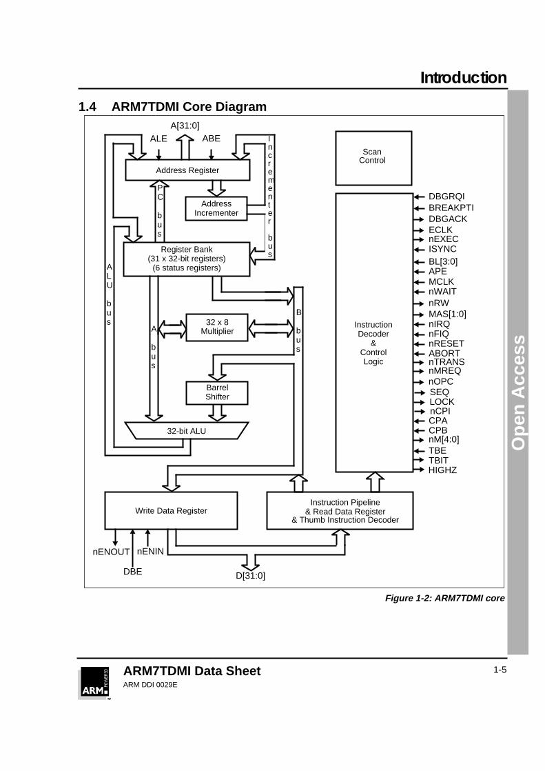
1.4 ARM7TDMI Core Diagram
Figure 1-2: ARM7TDMI core
nRESET
nMREQ
SEQ
ABORT
nIRQnFIQ
nRW
LOCKnCPICPACPB
nWAITMCLK
nOPC
nTRANS
InstructionDecoder
&ControlLogic
Instruction Pipeline& Read Data Register
DBE D[31:0]
32-bit ALU
BarrelShifter
AddressIncrementer
Address Register
Register Bank(31 x 32-bit registers)
(6 status registers)
A[31:0]ALE
Multiplier
ABE
Write Data Register
nM[4:0]
32 x 8
nENOUT nENIN
TBE
ScanControl
BREAKPTIDBGRQI
nEXEC
DBGACKECLK
ISYNC
B
bus
ALU
bus
A
bus
PC
bus
Incrementer
bus
APEBL[3:0]
MAS[1:0]
TBITHIGHZ
& Thumb Instruction Decoder
Introduction
ARM7TDMI Data SheetARM DDI 0029E
1-6
Ope
n A
cces
s
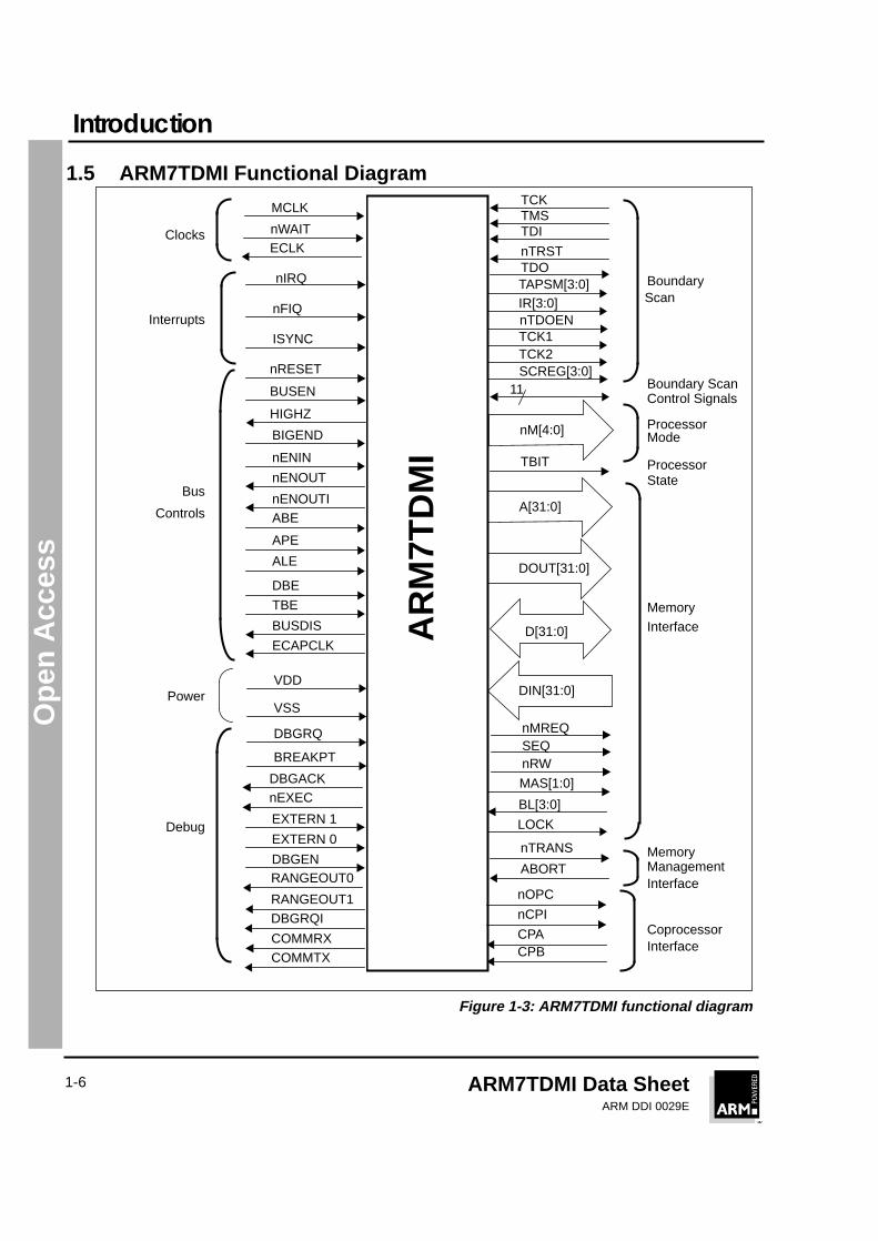
1.5 ARM7TDMI Functional Diagram
Figure 1-3: ARM7TDMI functional diagram
LOCK
A[31:0]
ABORTMemoryManagement
nOPC
nCPI
CPACPB
CoprocessorInterface
nTRANS
MemoryInterface
Interface
D[31:0]
TCKTMSTDI
nTRST
BoundaryScan
TDO
ProcessorMode
nRW
nMREQSEQ
BL[3:0]
MAS[1:0]
APE
TBIT ProcessorState
nM[4:0]A
RM
7TD
MI
DIN[31:0]
DOUT[31:0]
TAPSM[3:0]IR[3:0]
Boundary Scan
TCK1TCK2
11Control Signals
nTDOEN
SCREG[3:0]
ABE
ALE
nIRQ
nFIQ
Bus
Interrupts
ISYNC
nRESET
MCLK
nWAITClocks
VDD
VSSPower
DBGRQ
BREAKPT
DBGACKnEXEC
Debug
Controls
EXTERN 1
DBE
TBE
EXTERN 0
nENOUT
nENIN
ECLK
DBGEN
APE
HIGHZ
BIGEND
BUSEN
RANGEOUT0
RANGEOUT1DBGRQI
COMMRXCOMMTX
nENOUTI
ECAPCLK
BUSDIS
ARM7TDMI Data SheetARM DDI 0029E
2-1
111
Ope
n A
cces
s
Signal Description
This chapter lists and describes the signals for the ARM7TDMI.
2.1 Signal Description 2-2
2
Signal Description
ARM7TDMI Data SheetARM DDI 0029E
2-2
Ope
n A
cces
s
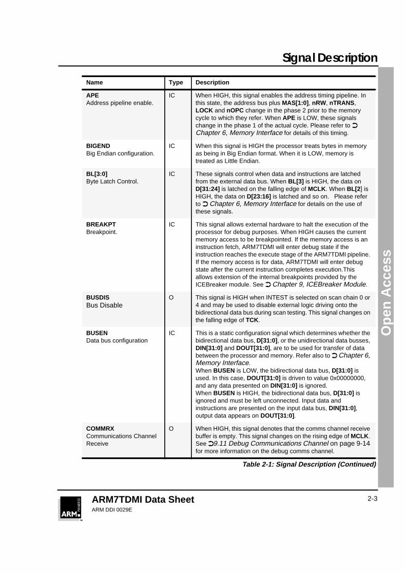
2.1 Signal DescriptionThe following table lists and describes all the signals for the ARM7TDMI.
Transistor sizes
For a 0.6 µm ARM7TDMI:
INV4 driver has transistor sizes of p = 22.32 µm/0.6 µmN = 12.6 µm/0.6 µm
INV8 driver has transistor sizes of p = 44.64 µm/0.6 µmN = 25.2 µm/0.6 µm
Key to signal types
IC Input CMOS thresholdsP PowerO4 Output with INV4 driverO8 Output with INV8 driver
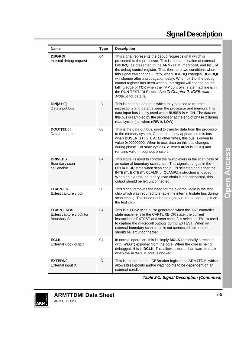
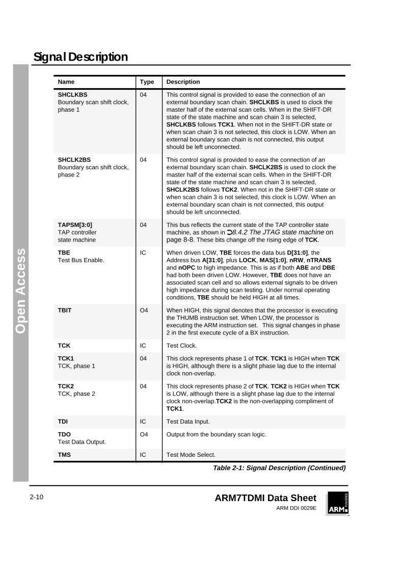
Name Type Description
A[31:0]Addresses
08 This is the processor address bus. If ALE (address latch enable)is HIGH and APE (Address Pipeline Enable) is LOW, theaddresses become valid during phase 2 of the cycle before theone to which they refer and remain so during phase 1 of thereferenced cycle. Their stable period may be controlled by ALEor APE as described below.
ABEAddress bus enable
IC This is an input signal which, when LOW, puts the address busdrivers into a high impedance state. This signal has a similareffect on the following control signals: MAS[1:0] , nRW, LOCK ,nOPC and nTRANS . ABE must be tied HIGH when there is nosystem requirement to turn off the address drivers.
ABORTMemory Abort
IC This is an input which allows the memory system to tell theprocessor that a requested access is not allowed.
ALEAddress latch enable.
IC This input is used to control transparent latches on the addressoutputs. Normally the addresses change during phase 2 to thevalue required during the next cycle, but for direct interfacing toROMs they are required to be stable to the end of phase 2.Taking ALE LOW until the end of phase 2 will ensure that thishappens. This signal has a similar effect on the following controlsignals: MAS[1:0] , nRW, LOCK , nOPC and nTRANS . If thesystem does not require address lines to be held in this way,ALE must be tied HIGH. The address latch is static, so ALE maybe held LOW for long periods to freeze addresses.
Table 2-1: Signal Description
Signal Description
ARM7TDMI Data SheetARM DDI 0029E
2-3
Ope
n A
cces
s
APEAddress pipeline enable.
IC When HIGH, this signal enables the address timing pipeline. Inthis state, the address bus plus MAS[1:0] , nRW, nTRANS ,LOCK and nOPC change in the phase 2 prior to the memorycycle to which they refer. When APE is LOW, these signalschange in the phase 1 of the actual cycle. Please refer to ➲Chapter 6, Memory Interface for details of this timing.
BIGENDBig Endian configuration.
IC When this signal is HIGH the processor treats bytes in memoryas being in Big Endian format. When it is LOW, memory istreated as Little Endian.
BL[3:0]Byte Latch Control.
IC These signals control when data and instructions are latchedfrom the external data bus. When BL[3] is HIGH, the data onD[31:24] is latched on the falling edge of MCLK . When BL[2 ] isHIGH, the data on D[23:16] is latched and so on. Please referto ➲ Chapter 6, Memory Interface for details on the use ofthese signals.
BREAKPTBreakpoint.
IC This signal allows external hardware to halt the execution of theprocessor for debug purposes. When HIGH causes the currentmemory access to be breakpointed. If the memory access is aninstruction fetch, ARM7TDMI will enter debug state if theinstruction reaches the execute stage of the ARM7TDMI pipeline.If the memory access is for data, ARM7TDMI will enter debugstate after the current instruction completes execution.Thisallows extension of the internal breakpoints provided by theICEBreaker module. See ➲ Chapter 9, ICEBreaker Module.
BUSDISBus Disable
O This signal is HIGH when INTEST is selected on scan chain 0 or4 and may be used to disable external logic driving onto thebidirectional data bus during scan testing. This signal changes onthe falling edge of TCK.
BUSENData bus configuration
IC This is a static configuration signal which determines whether thebidirectional data bus, D[31:0] , or the unidirectional data busses,DIN[31:0] and DOUT[31:0] , are to be used for transfer of databetween the processor and memory. Refer also to ➲ Chapter 6,Memory Interface.When BUSEN is LOW, the bidirectional data bus, D[31:0] isused. In this case, DOUT[31:0] is driven to value 0x00000000,and any data presented on DIN[31:0] is ignored.When BUSEN is HIGH, the bidirectional data bus, D[31:0] isignored and must be left unconnected. Input data andinstructions are presented on the input data bus, DIN[31:0] ,output data appears on DOUT[31:0] .
COMMRXCommunications ChannelReceive
O When HIGH, this signal denotes that the comms channel receivebuffer is empty. This signal changes on the rising edge of MCLK .See ➲9.11 Debug Communications Channel on page 9-14for more information on the debug comms channel.
Name Type Description
Table 2-1: Signal Description (Continued)

Signal Description
ARM7TDMI Data SheetARM DDI 0029E
2-4
Ope
n A
cces
s
COMMTXCommunications ChannelTransmit
O When HIGH, this signal denotes that the comms channeltransmit buffer is empty. This signal changes on the rising edgeof MCLK . See ➲9.11 Debug Communications Channel onpage 9-14 for more information on the debug comms channel.
CPACoprocessor absent.
IC A coprocessor which is capable of performing the operation thatARM7TDMI is requesting (by asserting nCPI) should take CPALOW immediately. If CPA is HIGH at the end of phase 1 of thecycle in which nCPI went LOW, ARM7TDMI will abort thecoprocessor handshake and take the undefined instruction trap.If CPA is LOW and remains LOW, ARM7TDMI will busy-wait untilCPB is LOW and then complete the coprocessor instruction.
CPBCoprocessor busy.
IC A coprocessor which is capable of performing the operationwhich ARM7TDMI is requesting (by asserting nCPI), but cannotcommit to starting it immediately, should indicate this by drivingCPB HIGH. When the coprocessor is ready to start it should takeCPB LOW. ARM7TDMI samples CPB at the end of phase 1 ofeach cycle in which nCPI is LOW.
D[31:0]Data Bus.
IC08
These are bidirectional signal paths which are used for datatransfers between the processor and external memory. Duringread cycles (when nRW is LOW), the input data must be validbefore the end of phase 2 of the transfer cycle. During writecycles (when nRW is HIGH), the output data will become validduring phase 1 and remain valid throughout phase 2 of thetransfer cycle.Note that this bus is driven at all times, irrespective of whetherBUSEN is HIGH or LOW. When D[31:0] is not being used toconnect to the memory system it must be left unconnected. See➲ Chapter 6, Memory Interface.
DBEData Bus Enable.
IC This is an input signal which, when driven LOW, puts the databus D[31:0] into the high impedance state. This is included fortest purposes, and should be tied HIGH at all times.
DBGACKDebug acknowledge.
04 When HIGH indicates ARM is in debug state.
DBGENDebug Enable.
IC This input signal allows the debug features of ARM7TDMI to bedisabled. This signal should be driven LOW when debugging isnot required.
DBGRQDebug request.
IC This is a level-sensitive input, which when HIGH causesARM7TDMI to enter debug state after executing the currentinstruction. This allows external hardware to force ARM7TDMIinto the debug state, in addition to the debugging featuresprovided by the ICEBreaker block. See ➲ Chapter 9,ICEBreaker Module for details.
Name Type Description
Table 2-1: Signal Description (Continued)
Signal Description
ARM7TDMI Data SheetARM DDI 0029E
2-5
Ope
n A
cces
s
DBGRQIInternal debug request
04 This signal represents the debug request signal which ispresented to the processor. This is the combination of externalDBGRQ, as presented to the ARM7TDMI macrocell, and bit 1 ofthe debug control register. Thus there are two conditions wherethis signal can change. Firstly, when DBGRQ changes, DBGRQIwill change after a propagation delay. When bit 1 of the debugcontrol register has been written, this signal will change on thefalling edge of TCK when the TAP controller state machine is inthe RUN-TEST/IDLE state. See ➲ Chapter 9, ICEBreakerModule for details.
DIN[31:0]Data input bus
IC This is the input data bus which may be used to transferinstructions and data between the processor and memory.Thisdata input bus is only used when BUSEN is HIGH. The data onthis bus is sampled by the processor at the end of phase 2 duringread cycles (i.e. when nRW is LOW).
DOUT[31:0]Data output bus
08 This is the data out bus, used to transfer data from the processorto the memory system. Output data only appears on this buswhen BUSEN is HIGH. At all other times, this bus is driven tovalue 0x00000000. When in use, data on this bus changesduring phase 1 of store cycles (i.e. when nRW is HIGH) andremains valid throughout phase 2.
DRIVEBSBoundary scancell enable
04 This signal is used to control the multiplexers in the scan cells ofan external boundary scan chain. This signal changes in theUPDATE-IR state when scan chain 3 is selected and either theINTEST, EXTEST, CLAMP or CLAMPZ instruction is loaded.When an external boundary scan chain is not connected, thisoutput should be left unconnected.
ECAPCLKExtest capture clock
O This signal removes the need for the external logic in the testchip which was required to enable the internal tristate bus duringscan testing. This need not be brought out as an external pin onthe test chip.
ECAPCLKBSExtest capture clock forBoundary Scan
04 This is a TCK2 wide pulse generated when the TAP controllerstate machine is in the CAPTURE-DR state, the currentinstruction is EXTEST and scan chain 3 is selected. This is usedto capture the macrocell outputs during EXTEST. When anexternal boundary scan chain is not connected, this outputshould be left unconnected.
ECLKExternal clock output.
04 In normal operation, this is simply MCLK (optionally stretchedwith nWAIT ) exported from the core. When the core is beingdebugged, this is DCLK . This allows external hardware to trackwhen the ARM7DM core is clocked.
EXTERN0External input 0.
IC This is an input to the ICEBreaker logic in the ARM7TDMI whichallows breakpoints and/or watchpoints to be dependent on anexternal condition.
Name Type Description
Table 2-1: Signal Description (Continued)

Signal Description
ARM7TDMI Data SheetARM DDI 0029E
2-6
Ope
n A
cces
s
EXTERN1External input 1.
IC This is an input to the ICEBreaker logic in the ARM7TDMI whichallows breakpoints and/or watchpoints to be dependent on anexternal condition.
HIGHZ 04 This signal denotes that the HIGHZ instruction has been loadedinto the TAP controller. See ➲ Chapter 8, Debug Interface fordetails.
ICAPCLKBSIntest capture clock
04 This is a TCK2 wide pulse generated when the TAP controllerstate machine is in the CAPTURE-DR state, the currentinstruction is INTEST and scan chain 3 is selected. This is usedto capture the macrocell outputs during INTEST. When anexternal boundary scan chain is not connected, this outputshould be left unconnected.
IR[3:0]TAP controller Instructionregister
04 These 4 bits reflect the current instruction loaded into the TAPcontroller instruction register. The instruction encoding is asdescribed in ➲8.8 Public Instructions on page 8-9. These bitschange on the falling edge of TCK when the state machine is inthe UPDATE-IR state.
ISYNCSynchronous interrupts.
IC When LOW indicates that the nIRQ and nFIQ inputs are to besynchronised by the ARM core. When HIGH disables thissynchronisation for inputs that are already synchronous.
LOCKLocked operation.
08 When LOCK is HIGH, the processor is performing a “locked”memory access, and the memory controller must wait until LOCKgoes LOW before allowing another device to access the memory.LOCK changes while MCLK is HIGH, and remains HIGH for theduration of the locked memory accesses. It is active only duringthe data swap (SWP) instruction. The timing of this signal may bemodified by the use of ALE and APE in a similar way to theaddress, please refer to the ALE and APE descriptions. Thissignal may also be driven to a high impedance state by drivingABE LOW.
MAS[1:0]Memory Access Size.
08 These are output signals used by the processor to indicate to theexternal memory system when a word transfer or a half-word orbyte length is required. The signals take the value 10 (binary) forwords, 01 for half-words and 00 for bytes. 11 is reserved. Thesevalues are valid for both read and write cycles. The signals willnormally become valid during phase 2 of the cycle before the onein which the transfer will take place. They will remain stablethroughout phase 1 of the transfer cycle. The timing of thesignals may be modified by the use of ALE and APE in a similarway to the address, please refer to the ALE and APEdescriptions. The signals may also be driven to high impedancestate by driving ABE LOW.
Name Type Description
Table 2-1: Signal Description (Continued)
Signal Description
ARM7TDMI Data SheetARM DDI 0029E
2-7
Ope
n A
cces
s
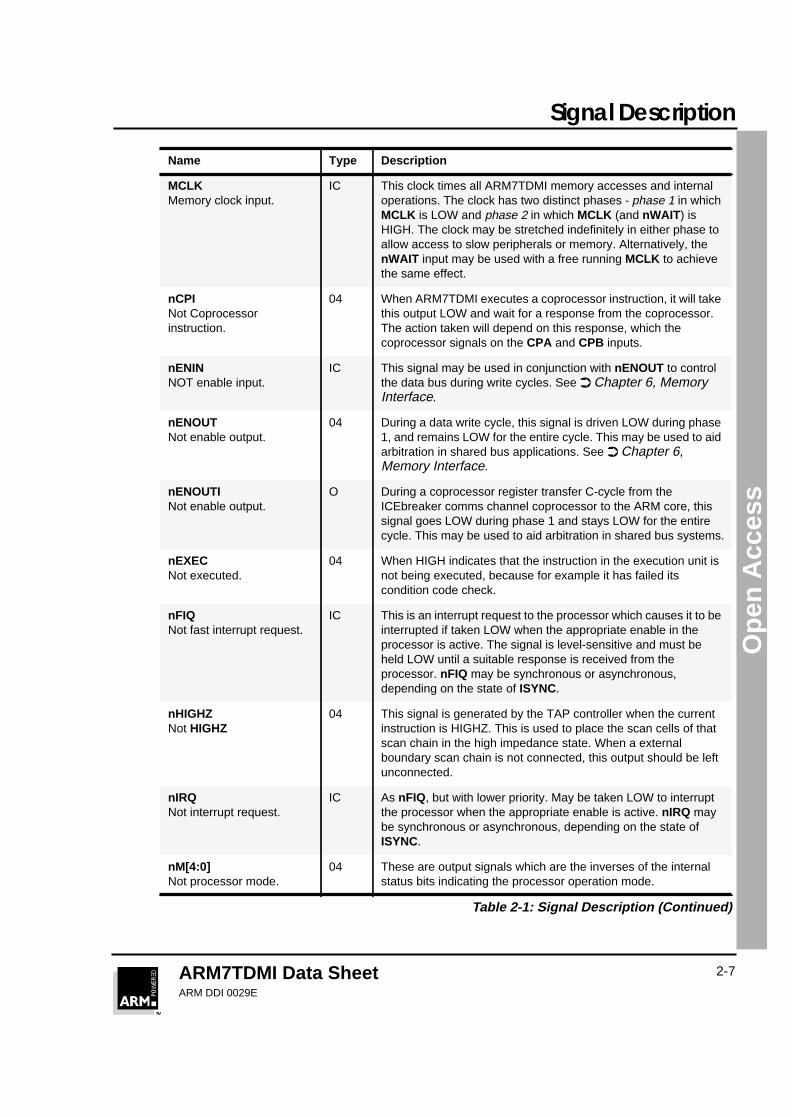
MCLKMemory clock input.
IC This clock times all ARM7TDMI memory accesses and internaloperations. The clock has two distinct phases - phase 1 in whichMCLK is LOW and phase 2 in which MCLK (and nWAIT ) isHIGH. The clock may be stretched indefinitely in either phase toallow access to slow peripherals or memory. Alternatively, thenWAIT input may be used with a free running MCLK to achievethe same effect.
nCPINot Coprocessorinstruction.
04 When ARM7TDMI executes a coprocessor instruction, it will takethis output LOW and wait for a response from the coprocessor.The action taken will depend on this response, which thecoprocessor signals on the CPA and CPB inputs.
nENINNOT enable input.
IC This signal may be used in conjunction with nENOUT to controlthe data bus during write cycles. See ➲ Chapter 6, MemoryInterface.
nENOUTNot enable output.
04 During a data write cycle, this signal is driven LOW during phase1, and remains LOW for the entire cycle. This may be used to aidarbitration in shared bus applications. See ➲ Chapter 6,Memory Interface.
nENOUTINot enable output.
O During a coprocessor register transfer C-cycle from theICEbreaker comms channel coprocessor to the ARM core, thissignal goes LOW during phase 1 and stays LOW for the entirecycle. This may be used to aid arbitration in shared bus systems.
nEXECNot executed.
04 When HIGH indicates that the instruction in the execution unit isnot being executed, because for example it has failed itscondition code check.
nFIQNot fast interrupt request.
IC This is an interrupt request to the processor which causes it to beinterrupted if taken LOW when the appropriate enable in theprocessor is active. The signal is level-sensitive and must beheld LOW until a suitable response is received from theprocessor. nFIQ may be synchronous or asynchronous,depending on the state of ISYNC.
nHIGHZNot HIGHZ
04 This signal is generated by the TAP controller when the currentinstruction is HIGHZ. This is used to place the scan cells of thatscan chain in the high impedance state. When a externalboundary scan chain is not connected, this output should be leftunconnected.
nIRQNot interrupt request.
IC As nFIQ, but with lower priority. May be taken LOW to interruptthe processor when the appropriate enable is active. nIRQ maybe synchronous or asynchronous, depending on the state ofISYNC.
nM[4:0]Not processor mode.
04 These are output signals which are the inverses of the internalstatus bits indicating the processor operation mode.
Name Type Description
Table 2-1: Signal Description (Continued)
Signal Description
ARM7TDMI Data SheetARM DDI 0029E
2-8
Ope
n A
cces
s
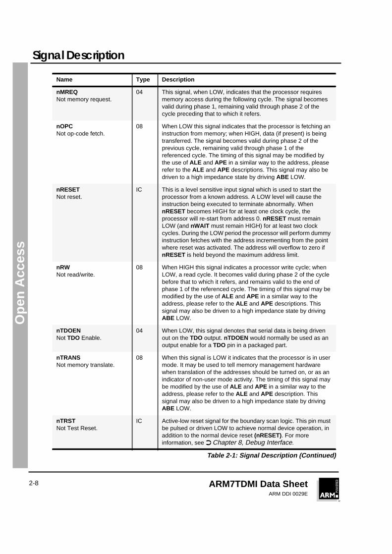
nMREQNot memory request.
04 This signal, when LOW, indicates that the processor requiresmemory access during the following cycle. The signal becomesvalid during phase 1, remaining valid through phase 2 of thecycle preceding that to which it refers.
nOPCNot op-code fetch.
08 When LOW this signal indicates that the processor is fetching aninstruction from memory; when HIGH, data (if present) is beingtransferred. The signal becomes valid during phase 2 of theprevious cycle, remaining valid through phase 1 of thereferenced cycle. The timing of this signal may be modified bythe use of ALE and APE in a similar way to the address, pleaserefer to the ALE and APE descriptions. This signal may also bedriven to a high impedance state by driving ABE LOW.
nRESETNot reset.
IC This is a level sensitive input signal which is used to start theprocessor from a known address. A LOW level will cause theinstruction being executed to terminate abnormally. WhennRESET becomes HIGH for at least one clock cycle, theprocessor will re-start from address 0. nRESET must remainLOW (and nWAIT must remain HIGH) for at least two clockcycles. During the LOW period the processor will perform dummyinstruction fetches with the address incrementing from the pointwhere reset was activated. The address will overflow to zero ifnRESET is held beyond the maximum address limit.
nRWNot read/write.
08 When HIGH this signal indicates a processor write cycle; whenLOW, a read cycle. It becomes valid during phase 2 of the cyclebefore that to which it refers, and remains valid to the end ofphase 1 of the referenced cycle. The timing of this signal may bemodified by the use of ALE and APE in a similar way to theaddress, please refer to the ALE and APE descriptions. Thissignal may also be driven to a high impedance state by drivingABE LOW.
nTDOENNot TDO Enable.
04 When LOW, this signal denotes that serial data is being drivenout on the TDO output. nTDOEN would normally be used as anoutput enable for a TDO pin in a packaged part.
nTRANSNot memory translate.
08 When this signal is LOW it indicates that the processor is in usermode. It may be used to tell memory management hardwarewhen translation of the addresses should be turned on, or as anindicator of non-user mode activity. The timing of this signal maybe modified by the use of ALE and APE in a similar way to theaddress, please refer to the ALE and APE description. Thissignal may also be driven to a high impedance state by drivingABE LOW.
nTRSTNot Test Reset.
IC Active-low reset signal for the boundary scan logic. This pin mustbe pulsed or driven LOW to achieve normal device operation, inaddition to the normal device reset (nRESET). For moreinformation, see ➲ Chapter 8, Debug Interface.
Name Type Description
Table 2-1: Signal Description (Continued)
Signal Description
ARM7TDMI Data SheetARM DDI 0029E
2-9
Ope
n A
cces
s
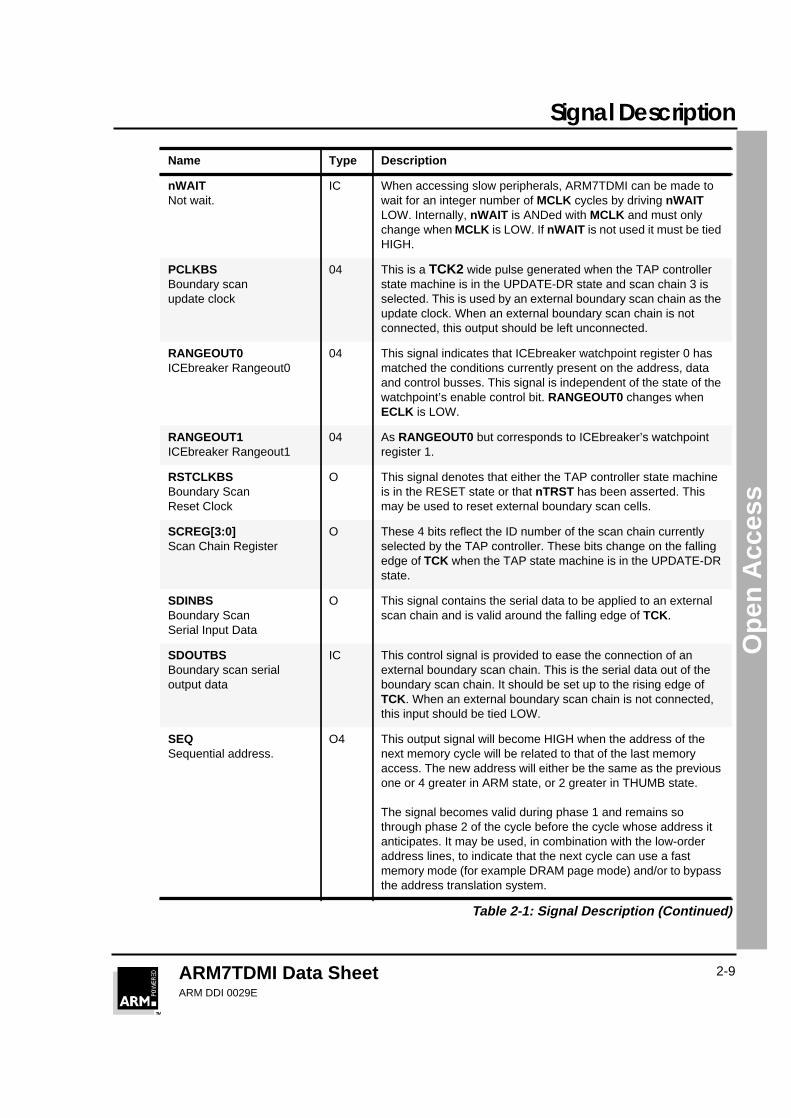
nWAITNot wait.
IC When accessing slow peripherals, ARM7TDMI can be made towait for an integer number of MCLK cycles by driving nWAITLOW. Internally, nWAIT is ANDed with MCLK and must onlychange when MCLK is LOW. If nWAIT is not used it must be tiedHIGH.
PCLKBSBoundary scanupdate clock
04 This is a TCK2 wide pulse generated when the TAP controllerstate machine is in the UPDATE-DR state and scan chain 3 isselected. This is used by an external boundary scan chain as theupdate clock. When an external boundary scan chain is notconnected, this output should be left unconnected.
RANGEOUT0ICEbreaker Rangeout0
04 This signal indicates that ICEbreaker watchpoint register 0 hasmatched the conditions currently present on the address, dataand control busses. This signal is independent of the state of thewatchpoint’s enable control bit. RANGEOUT0 changes whenECLK is LOW.
RANGEOUT1ICEbreaker Rangeout1
04 As RANGEOUT0 but corresponds to ICEbreaker’s watchpointregister 1.
RSTCLKBSBoundary ScanReset Clock
O This signal denotes that either the TAP controller state machineis in the RESET state or that nTRST has been asserted. Thismay be used to reset external boundary scan cells.
SCREG[3:0]Scan Chain Register
O These 4 bits reflect the ID number of the scan chain currentlyselected by the TAP controller. These bits change on the fallingedge of TCK when the TAP state machine is in the UPDATE-DRstate.
SDINBSBoundary ScanSerial Input Data
O This signal contains the serial data to be applied to an externalscan chain and is valid around the falling edge of TCK.
SDOUTBSBoundary scan serialoutput data
IC This control signal is provided to ease the connection of anexternal boundary scan chain. This is the serial data out of theboundary scan chain. It should be set up to the rising edge ofTCK. When an external boundary scan chain is not connected,this input should be tied LOW.
SEQSequential address.
O4 This output signal will become HIGH when the address of thenext memory cycle will be related to that of the last memoryaccess. The new address will either be the same as the previousone or 4 greater in ARM state, or 2 greater in THUMB state.
The signal becomes valid during phase 1 and remains sothrough phase 2 of the cycle before the cycle whose address itanticipates. It may be used, in combination with the low-orderaddress lines, to indicate that the next cycle can use a fastmemory mode (for example DRAM page mode) and/or to bypassthe address translation system.
Name Type Description
Table 2-1: Signal Description (Continued)
Signal Description
ARM7TDMI Data SheetARM DDI 0029E
2-10
Ope
n A
cces
s
SHCLKBSBoundary scan shift clock,phase 1
04 This control signal is provided to ease the connection of anexternal boundary scan chain. SHCLKBS is used to clock themaster half of the external scan cells. When in the SHIFT-DRstate of the state machine and scan chain 3 is selected,SHCLKBS follows TCK1. When not in the SHIFT-DR state orwhen scan chain 3 is not selected, this clock is LOW. When anexternal boundary scan chain is not connected, this outputshould be left unconnected.
SHCLK2BSBoundary scan shift clock,phase 2
04 This control signal is provided to ease the connection of anexternal boundary scan chain. SHCLK2BS is used to clock themaster half of the external scan cells. When in the SHIFT-DRstate of the state machine and scan chain 3 is selected,SHCLK2BS follows TCK2. When not in the SHIFT-DR state orwhen scan chain 3 is not selected, this clock is LOW. When anexternal boundary scan chain is not connected, this outputshould be left unconnected.
TAPSM[3:0]TAP controllerstate machine
04 This bus reflects the current state of the TAP controller statemachine, as shown in ➲8.4.2 The JTAG state machine onpage 8-8. These bits change off the rising edge of TCK.
TBETest Bus Enable.
IC When driven LOW, TBE forces the data bus D[31:0] , theAddress bus A[31:0] , plus LOCK , MAS[1:0] , nRW, nTRANSand nOPC to high impedance. This is as if both ABE and DBEhad both been driven LOW. However, TBE does not have anassociated scan cell and so allows external signals to be drivenhigh impedance during scan testing. Under normal operatingconditions, TBE should be held HIGH at all times.
TBIT O4 When HIGH, this signal denotes that the processor is executingthe THUMB instruction set. When LOW, the processor isexecuting the ARM instruction set. This signal changes in phase2 in the first execute cycle of a BX instruction.
TCK IC Test Clock.
TCK1TCK, phase 1
04 This clock represents phase 1 of TCK. TCK1 is HIGH when TCKis HIGH, although there is a slight phase lag due to the internalclock non-overlap.
TCK2TCK, phase 2
04 This clock represents phase 2 of TCK. TCK2 is HIGH when TCKis LOW, although there is a slight phase lag due to the internalclock non-overlap.TCK2 is the non-overlapping compliment ofTCK1.
TDI IC Test Data Input.
TDOTest Data Output.
O4 Output from the boundary scan logic.
TMS IC Test Mode Select.
Name Type Description
Table 2-1: Signal Description (Continued)

Signal Description
ARM7TDMI Data SheetARM DDI 0029E
2-11
Ope
n A
cces
s
VDDPower supply.
P These connections provide power to the device.
VSSGround.
P These connections are the ground reference for all signals.
Name Type Description
Table 2-1: Signal Description (Continued)
Signal Description
ARM7TDMI Data SheetARM DDI 0029E
2-12
Ope
n A
cces
s
ARM7TDMI Data SheetARM DDI 0029E
3-1
111
Ope
n A
cces
s
Programmer’s Model
This chapter describes the two operating states of the ARM7TDMI.
3.1 Processor Operating States 3-2
3.2 Switching State 3-2
3.3 Memory Formats 3-2
3.4 Instruction Length 3-3
3.5 Data Types 3-3
3.6 Operating Modes 3-4
3.7 Registers 3-4
3.8 The Program Status Registers 3-8
3.9 Exceptions 3-10
3.11 Reset 3-15
3

Programmer’s Model
ARM7TDMI Data SheetARM DDI 0029E
3-2
Ope
n A
cces
s
3.1 Processor Operating StatesFrom the programmer’s point of view, the ARM7TDMI can be in one of two states:
ARM state which executes 32-bit, word-aligned ARM instructions.
THUMB state which operates with 16-bit, halfword-aligned THUMBinstructions. In this state, the PC uses bit 1 to select betweenalternate halfwords.
Note Transition between these two states does not affect the processor mode or thecontents of the registers.
3.2 Switching State
Entering THUMB state
Entry into THUMB state can be achieved by executing a BX instruction with the statebit (bit 0) set in the operand register.
Transition to THUMB state will also occur automatically on return from an exception(IRQ, FIQ, UNDEF, ABORT, SWI etc.), if the exception was entered with the processorin THUMB state.
Entering ARM state
Entry into ARM state happens:
1 On execution of the BX instruction with the state bit clear in the operandregister.
2 On the processor taking an exception (IRQ, FIQ, RESET, UNDEF, ABORT,SWI etc.).
In this case, the PC is placed in the exception mode’s link register, andexecution commences at the exception’s vector address.
3.3 Memory FormatsARM7TDMI views memory as a linear collection of bytes numbered upwards fromzero. Bytes 0 to 3 hold the first stored word, bytes 4 to 7 the second and so on.ARM7TDMI can treat words in memory as being stored either in Big Endian or LittleEndian format.
Programmer’s Model
ARM7TDMI Data SheetARM DDI 0029E
3-3
Ope
n A
cces
s
3.3.1 Big endian format
In Big Endian format, the most significant byte of a word is stored at the lowestnumbered byte and the least significant byte at the highest numbered byte. Byte 0 ofthe memory system is therefore connected to data lines 31 through 24.
3.3.2 Little endian format
In Little Endian format, the lowest numbered byte in a word is considered the word’sleast significant byte, and the highest numbered byte the most significant. Byte 0 ofthe memory system is therefore connected to data lines 7 through 0.
3.4 Instruction LengthInstructions are either 32 bits long (in ARM state) or 16 bits long (in THUMB state).
3.5 Data TypesARM7TDMI supports byte (8-bit), halfword (16-bit) and word (32-bit) data types.Words must be aligned to four-byte boundaries and half words to two-byte boundaries.
Higher Address 31 24 23 16 15 8 7 0 Word Address
8 9 10 11 8
4 5 6 7 4
0 1 2 3 0
Lower Address • Most significant byte is at lowest address• Word is addressed by byte address of most significant byte
Figure 3-1: Big endian addresses of bytes within words
Higher Address 31 24 23 16 15 8 7 0 Word Address
11 10 9 8 8
7 6 5 4 4
3 2 1 0 0
Lower Address • Least significant byte is at lowest address• Word is addressed by byte address of least significant byte
Figure 3-2: Little endian addresses of bytes within words

Programmer’s Model
ARM7TDMI Data SheetARM DDI 0029E
3-4
Ope
n A
cces
s
3.6 Operating ModesARM7TDMI supports seven modes of operation:
User (usr): The normal ARM program execution state
FIQ (fiq): Designed to support a data transfer or channel process
IRQ (irq): Used for general-purpose interrupt handling
Supervisor (svc): Protected mode for the operating system
Abort mode (abt): Entered after a data or instruction prefetch abort
System (sys): A privileged user mode for the operating system
Undefined (und): Entered when an undefined instruction is executed
Mode changes may be made under software control, or may be brought about byexternal interrupts or exception processing. Most application programs will execute inUser mode. The non-user modes - known as privileged modes - are entered in orderto service interrupts or exceptions, or to access protected resources.
3.7 RegistersARM7TDMI has a total of 37 registers - 31 general-purpose 32-bit registers and sixstatus registers - but these cannot all be seen at once. The processor state andoperating mode dictate which registers are available to the programmer.
3.7.1 The ARM state register set
In ARM state, 16 general registers and one or two status registers are visible at anyone time. In privileged (non-User) modes, mode-specific banked registers areswitched in. ➲Figure 3-3: Register organization in ARM state shows which registersare available in each mode: the banked registers are marked with a shaded triangle.
The ARM state register set contains 16 directly accessible registers: R0 to R15. All ofthese except R15 are general-purpose, and may be used to hold either data oraddress values. In addition to these, there is a seventeenth register used to storestatus information
Register 14 is used as the subroutine link register. This receives a copy ofR15 when a Branch and Link (BL) instruction is executed. Atall other times it may be treated as a general-purposeregister. The corresponding banked registers R14_svc,R14_irq, R14_fiq, R14_abt and R14_und are similarly usedto hold the return values of R15 when interrupts andexceptions arise, or when Branch and Link instructions areexecuted within interrupt or exception routines.
Register 15 holds the Program Counter (PC). In ARM state, bits [1:0] ofR15 are zero and bits [31:2] contain the PC. In THUMB state,bit [0] is zero and bits [31:1] contain the PC.
Register 16 is the CPSR (Current Program Status Register). Thiscontains condition code flags and the current mode bits.

Programmer’s Model
ARM7TDMI Data SheetARM DDI 0029E
3-5
Ope
n A
cces
s
FIQ mode has seven banked registers mapped to R8-14 (R8_fiq-R14_fiq). In ARMstate, many FIQ handlers do not need to save any registers. User, IRQ, Supervisor,Abort and Undefined each have two banked registers mapped to R13 and R14,allowing each of these modes to have a private stack pointer and link registers.
Figure 3-3: Register organization in ARM state
ARM State General Registers and Program Counter
R0
R1
R2
R3
R4
R5
R6
R7
R8
R9
R10
R11
R12
R13
R14
R15 (PC)
R0
R1
R2
R3
R4
R5
R6
R7
R8_fiq
R9_fiq
R10_fiq
R11_fiq
R12_fiq
R13_fiq
R14_fiq
R15 (PC)
R0
R1
R2
R3
R4
R5
R6
R7
R8
R9
R10
R11
R12
R13_svc
R14_svc
R15 (PC)
R0
R1
R2
R3
R4
R5
R6
R7
R8
R9
R10
R11
R12
R13_abt
R14_abt
R15 (PC)
R0
R1
R2
R3
R4
R5
R6
R7
R8
R9
R10
R11
R12
R13_irq
R14_irq
R15 (PC)
R0
R1
R2
R3
R4
R5
R6
R7
R8
R9
R10
R11
R12
R13_und
R14_und
R15 (PC)
System & User FIQ Supervisor Abort IRQ Undefined
CPSR CPSR
SPSR_fiq
CPSR
SPSR_svc
CPSR
SPSR_abt
CPSR
SPSR_irq
CPSR
SPSR_und
ARM State Program Status Registers
= banked register
Programmer’s Model
ARM7TDMI Data SheetARM DDI 0029E
3-6
Ope
n A
cces
s
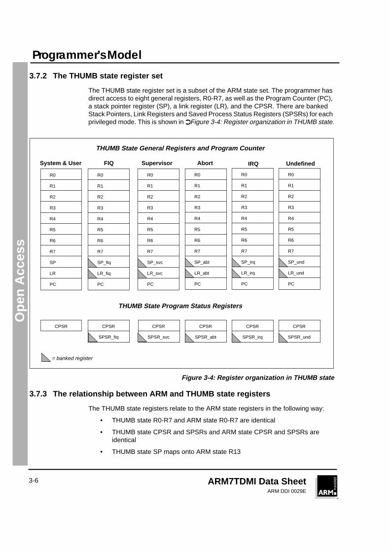
3.7.2 The THUMB state register set
The THUMB state register set is a subset of the ARM state set. The programmer hasdirect access to eight general registers, R0-R7, as well as the Program Counter (PC),a stack pointer register (SP), a link register (LR), and the CPSR. There are bankedStack Pointers, Link Registers and Saved Process Status Registers (SPSRs) for eachprivileged mode. This is shown in ➲Figure 3-4: Register organization in THUMB state.
Figure 3-4: Register organization in THUMB state
3.7.3 The relationship between ARM and THUMB state registers
The THUMB state registers relate to the ARM state registers in the following way:
• THUMB state R0-R7 and ARM state R0-R7 are identical
• THUMB state CPSR and SPSRs and ARM state CPSR and SPSRs areidentical
• THUMB state SP maps onto ARM state R13
R0
R1
R2
R3
R4
R5
R6
R7
SP
LR
PC
System & User FIQ Supervisor Abort IRQ Undefined
CPSR CPSR
SPSR_fiq
CPSR
SPSR_svc
CPSR
SPSR_abt
CPSR
SPSR_irq
CPSR
SPSR_und
R0
R1
R2
R3
R4
R5
R6
R7
SP_fiq
LR_fiq
PC
R0
R1
R2
R3
R4
R5
R6
R7
SP_svc
LR_svc
PC
R0
R1
R2
R3
R4
R5
R6
R7
SP_abt
LR_abt
PC
R0
R1
R2
R3
R4
R5
R6
R7
SP_irq
LR_irq
PC
R0
R1
R2
R3
R4
R5
R6
R7
SP_und
LR_und
PC
THUMB State General Registers and Program Counter
THUMB State Program Status Registers
= banked register
Programmer’s Model
ARM7TDMI Data SheetARM DDI 0029E
3-7
Ope
n A
cces
s
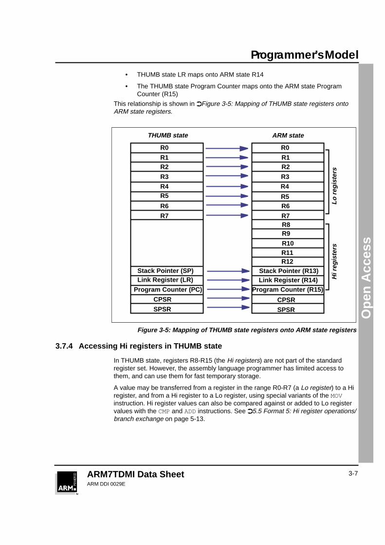
• THUMB state LR maps onto ARM state R14
• The THUMB state Program Counter maps onto the ARM state ProgramCounter (R15)
This relationship is shown in ➲Figure 3-5: Mapping of THUMB state registers ontoARM state registers.
Figure 3-5: Mapping of THUMB state registers onto ARM state registers
3.7.4 Accessing Hi registers in THUMB state
In THUMB state, registers R8-R15 (the Hi registers) are not part of the standardregister set. However, the assembly language programmer has limited access tothem, and can use them for fast temporary storage.
A value may be transferred from a register in the range R0-R7 (a Lo register) to a Hiregister, and from a Hi register to a Lo register, using special variants of the MOVinstruction. Hi register values can also be compared against or added to Lo registervalues with the CMP and ADD instructions. See ➲5.5 Format 5: Hi register operations/branch exchange on page 5-13.
R0
R1R2
R3
R5R6
R7R8R9
R10R11R12
Stack Pointer (R13)Link Register (R14)
Program Counter (R15)
R0
R1R2
R3
R5
R6
R7
Stack Pointer (SP)Link Register (LR)
Program Counter (PC)
CPSR CPSRSPSR SPSR
THUMB state ARM state
R4R4
Lo r
egis
ters
Hi r
egis
ters
Programmer’s Model
ARM7TDMI Data SheetARM DDI 0029E
3-8
Ope
n A
cces
s
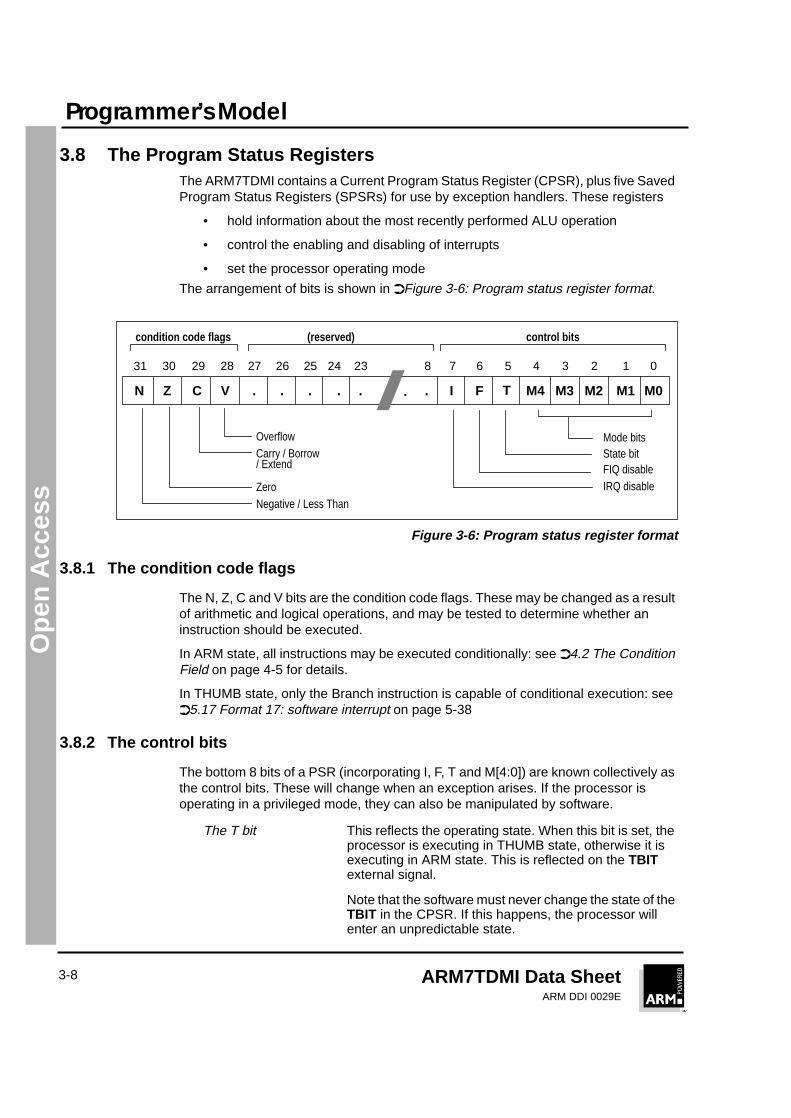
3.8 The Program Status RegistersThe ARM7TDMI contains a Current Program Status Register (CPSR), plus five SavedProgram Status Registers (SPSRs) for use by exception handlers. These registers
• hold information about the most recently performed ALU operation
• control the enabling and disabling of interrupts
• set the processor operating mode
The arrangement of bits is shown in ➲Figure 3-6: Program status register format.
Figure 3-6: Program status register format
3.8.1 The condition code flags
The N, Z, C and V bits are the condition code flags. These may be changed as a resultof arithmetic and logical operations, and may be tested to determine whether aninstruction should be executed.
In ARM state, all instructions may be executed conditionally: see ➲4.2 The ConditionField on page 4-5 for details.
In THUMB state, only the Branch instruction is capable of conditional execution: see➲5.17 Format 17: software interrupt on page 5-38
3.8.2 The control bits
The bottom 8 bits of a PSR (incorporating I, F, T and M[4:0]) are known collectively asthe control bits. These will change when an exception arises. If the processor isoperating in a privileged mode, they can also be manipulated by software.
The T bit This reflects the operating state. When this bit is set, theprocessor is executing in THUMB state, otherwise it isexecuting in ARM state. This is reflected on the TBITexternal signal.
Note that the software must never change the state of theTBIT in the CPSR. If this happens, the processor willenter an unpredictable state.
0123456782728293031
M0M1M2M3M4. FIVCZN
OverflowCarry / Borrow
ZeroNegative / Less Than
Mode bits
FIQ disableIRQ disable
. .
condition code flags control bits
State bit
(reserved)
23
. .
24
T
25
.
26
.
/ Extend
Programmer’s Model
ARM7TDMI Data SheetARM DDI 0029E
3-9
Ope
n A
cces
s
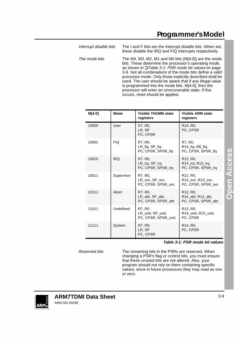
Interrupt disable bits The I and F bits are the interrupt disable bits. When set,these disable the IRQ and FIQ interrupts respectively.
The mode bits The M4, M3, M2, M1 and M0 bits (M[4:0]) are the modebits. These determine the processor’s operating mode,as shown in ➲Table 3-1: PSR mode bit values on page3-9. Not all combinations of the mode bits define a validprocessor mode. Only those explicitly described shall beused. The user should be aware that if any illegal valueis programmed into the mode bits, M[4:0], then theprocessor will enter an unrecoverable state. If thisoccurs, reset should be applied.
Reserved bits The remaining bits in the PSRs are reserved. Whenchanging a PSR’s flag or control bits, you must ensurethat these unused bits are not altered. Also, yourprogram should not rely on them containing specificvalues, since in future processors they may read as oneor zero.
M[4:0] Mode Visible THUMB stateregisters
Visible ARM stateregisters
10000 User R7..R0,LR, SPPC, CPSR
R14..R0,PC, CPSR
10001 FIQ R7..R0,LR_fiq, SP_fiqPC, CPSR, SPSR_fiq
R7..R0,R14_fiq..R8_fiq,PC, CPSR, SPSR_fiq
10010 IRQ R7..R0,LR_irq, SP_irqPC, CPSR, SPSR_irq
R12..R0,R14_irq..R13_irq,PC, CPSR, SPSR_irq
10011 Supervisor R7..R0,LR_svc, SP_svc,PC, CPSR, SPSR_svc
R12..R0,R14_svc..R13_svc,PC, CPSR, SPSR_svc
10111 Abort R7..R0,LR_abt, SP_abt,PC, CPSR, SPSR_abt
R12..R0,R14_abt..R13_abt,PC, CPSR, SPSR_abt
11011 Undefined R7..R0LR_und, SP_und,PC, CPSR, SPSR_und
R12..R0,R14_und..R13_und,PC, CPSR
11111 System R7..R0,LR, SPPC, CPSR
R14..R0,PC, CPSR
Table 3-1: PSR mode bit values
Programmer’s Model
ARM7TDMI Data SheetARM DDI 0029E
3-10
Ope
n A
cces
s
3.9 ExceptionsExceptions arise whenever the normal flow of a program has to be halted temporarily,for example to service an interrupt from a peripheral. Before an exception can behandled, the current processor state must be preserved so that the original programcan resume when the handler routine has finished.
It is possible for several exceptions to arise at the same time. If this happens, they aredealt with in a fixed order - see ➲3.9.10 Exception priorities on page 3-14.
3.9.1 Action on entering an exception
When handling an exception, the ARM7TDMI:
1 Preserves the address of the next instruction in the appropriate Link Register.If the exception has been entered from ARM state, then the address of thenext instruction is copied into the Link Register (that is, current PC + 4 or PC+ 8 depending on the exception. See ➲Table 3-2: Exception entry/exit onpage 3-11 for details). If the exception has been entered from THUMB state,then the value written into the Link Register is the current PC offset by a valuesuch that the program resumes from the correct place on return from theexception. This means that the exception handler need not determine whichstate the exception was entered from. For example, in the case of SWI, MOVSPC, R14_svc will always return to the next instruction regardless of whetherthe SWI was executed in ARM or THUMB state.
2 Copies the CPSR into the appropriate SPSR
3 Forces the CPSR mode bits to a value which depends on the exception
4 Forces the PC to fetch the next instruction from the relevant exception vector
It may also set the interrupt disable flags to prevent otherwise unmanageable nestingsof exceptions.
If the processor is in THUMB state when an exception occurs, it will automaticallyswitch into ARM state when the PC is loaded with the exception vector address.
3.9.2 Action on leaving an exception
On completion, the exception handler:
1 Moves the Link Register, minus an offset where appropriate, to the PC. (Theoffset will vary depending on the type of exception.)
2 Copies the SPSR back to the CPSR
3 Clears the interrupt disable flags, if they were set on entry
Note An explicit switch back to THUMB state is never needed, since restoring the CPSRfrom the SPSR automatically sets the T bit to the value it held immediately prior to theexception.

Programmer’s Model
ARM7TDMI Data SheetARM DDI 0029E
3-11
Ope
n A
cces
s
3.9.3 Exception entry/exit summary
➲Table 3-2: Exception entry/exit summarises the PC value preserved in the relevantR14 on exception entry, and the recommended instruction for exiting the exceptionhandler.
Notes
1 Where PC is the address of the BL/SWI/Undefined Instruction fetch which hadthe prefetch abort.
2 Where PC is the address of the instruction which did not get executed sincethe FIQ or IRQ took priority.
3 Where PC is the address of the Load or Store instruction which generated thedata abort.
4 The value saved in R14_svc upon reset is unpredictable.
3.9.4 FIQ
The FIQ (Fast Interrupt Request) exception is designed to support a data transfer orchannel process, and in ARM state has sufficient private registers to remove the needfor register saving (thus minimising the overhead of context switching).
FIQ is externally generated by taking the nFIQ input LOW. This input can except eithersynchronous or asynchronous transitions, depending on the state of the ISYNC inputsignal. When ISYNC is LOW, nFIQ and nIRQ are considered asynchronous, and acycle delay for synchronization is incurred before the interrupt can affect the processorflow.
Irrespective of whether the exception was entered from ARM or Thumb state, a FIQhandler should leave the interrupt by executing
SUBS PC,R14_fiq,#4
Return Instruction Previous StateARM THUMBR14_x R14_x
Notes
BL MOV PC, R14 PC + 4 PC + 2 1
SWI MOVS PC, R14_svc PC + 4 PC + 2 1
UDEF MOVS PC, R14_und PC + 4 PC + 2 1
FIQ SUBS PC, R14_fiq, #4 PC + 4 PC + 4 2
IRQ SUBS PC, R14_irq, #4 PC + 4 PC + 4 2
PABT SUBS PC, R14_abt, #4 PC + 4 PC + 4 1
DABT SUBS PC, R14_abt, #8 PC + 8 PC + 8 3
RESET NA - - 4
Table 3-2: Exception entry/exit

Programmer’s Model
ARM7TDMI Data SheetARM DDI 0029E
3-12
Ope
n A
cces
s
FIQ may be disabled by setting the CPSR’s F flag (but note that this is not possiblefrom User mode). If the F flag is clear, ARM7TDMI checks for a LOW level on theoutput of the FIQ synchroniser at the end of each instruction.
3.9.5 IRQ
The IRQ (Interrupt Request) exception is a normal interrupt caused by a LOW level onthe nIRQ input. IRQ has a lower priority than FIQ and is masked out when a FIQsequence is entered. It may be disabled at any time by setting the I bit in the CPSR,though this can only be done from a privileged (non-User) mode.
Irrespective of whether the exception was entered from ARM or Thumb state, an IRQhandler should return from the interrupt by executing
SUBS PC,R14_irq,#4
3.9.6 Abort
An abort indicates that the current memory access cannot be completed. It can besignalled by the external ABORT input. ARM7TDMI checks for the abort exceptionduring memory access cycles.
There are two types of abort:
Prefetch abort occurs during an instruction prefetch.
Data abort occurs during a data access.
If a prefetch abort occurs, the prefetched instruction is marked as invalid, but theexception will not be taken until the instruction reaches the head of the pipeline. If theinstruction is not executed - for example because a branch occurs while it is in thepipeline - the abort does not take place.
If a data abort occurs, the action taken depends on the instruction type:
1 Single data transfer instructions (LDR, STR) write back modified baseregisters: the Abort handler must be aware of this.
2 The swap instruction (SWP) is aborted as though it had not been executed.
3 Block data transfer instructions (LDM, STM) complete. If write-back is set, thebase is updated. If the instruction would have overwritten the base with data(ie it has the base in the transfer list), the overwriting is prevented. All registeroverwriting is prevented after an abort is indicated, which means in particularthat R15 (always the last register to be transferred) is preserved in an abortedLDM instruction.
The abort mechanism allows the implementation of a demand paged virtual memorysystem. In such a system the processor is allowed to generate arbitrary addresses.When the data at an address is unavailable, the Memory Management Unit (MMU)signals an abort. The abort handler must then work out the cause of the abort, makethe requested data available, and retry the aborted instruction. The applicationprogram needs no knowledge of the amount of memory available to it, nor is its statein any way affected by the abort.
Programmer’s Model
ARM7TDMI Data SheetARM DDI 0029E
3-13
Ope
n A
cces
s
After fixing the reason for the abort, the handler should execute the followingirrespective of the state (ARM or Thumb):
SUBS PC,R14_abt,#4 for a prefetch abort, or
SUBS PC,R14_abt,#8 for a data abort
This restores both the PC and the CPSR, and retries the aborted instruction.
3.9.7 Software interrupt
The software interrupt instruction (SWI) is used for entering Supervisor mode, usuallyto request a particular supervisor function. A SWI handler should return by executingthe following irrespective of the state (ARM or Thumb):
MOV PC, R14_svc
This restores the PC and CPSR, and returns to the instruction following the SWI.
3.9.8 Undefined instruction
When ARM7TDMI comes across an instruction which it cannot handle, it takes theundefined instruction trap. This mechanism may be used to extend either the THUMBor ARM instruction set by software emulation.
After emulating the failed instruction, the trap handler should execute the followingirrespective of the state (ARM or Thumb):
MOVS PC,R14_und
This restores the CPSR and returns to the instruction following the undefinedinstruction.
3.9.9 Exception vectors
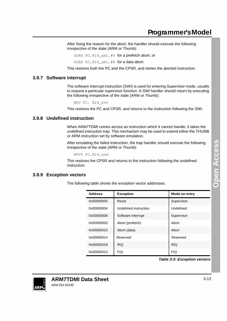
The following table shows the exception vector addresses.
Address Exception Mode on entry
0x00000000 Reset Supervisor
0x00000004 Undefined instruction Undefined
0x00000008 Software interrupt Supervisor
0x0000000C Abort (prefetch) Abort
0x00000010 Abort (data) Abort
0x00000014 Reserved Reserved
0x00000018 IRQ IRQ
0x0000001C FIQ FIQ
Table 3-3: Exception vectors
Programmer’s Model
ARM7TDMI Data SheetARM DDI 0029E
3-14
Ope
n A
cces
s
3.9.10 Exception priorities
When multiple exceptions arise at the same time, a fixed priority system determinesthe order in which they are handled:
Highest priority:
1 Reset
2 Data abort
3 FIQ
4 IRQ
5 Prefetch abort
Lowest priority:
6 Undefined Instruction, Software interrupt.
Not all exceptions can occur at once:
Undefined Instruction and Software Interrupt are mutually exclusive, since they eachcorrespond to particular (non-overlapping) decodings of the current instruction.
If a data abort occurs at the same time as a FIQ, and FIQs are enabled (ie the CPSR’sF flag is clear), ARM7TDMI enters the data abort handler and then immediatelyproceeds to the FIQ vector. A normal return from FIQ will cause the data abort handlerto resume execution. Placing data abort at a higher priority than FIQ is necessary toensure that the transfer error does not escape detection. The time for this exceptionentry should be added to worst-case FIQ latency calculations.
3.10 Interrupt LatenciesThe worst case latency for FIQ, assuming that it is enabled, consists of the longesttime the request can take to pass through the synchroniser (Tsyncmax ifasynchronous), plus the time for the longest instruction to complete (Tldm, the longestinstruction is an LDM which loads all the registers including the PC), plus the time forthe data abort entry (Texc), plus the time for FIQ entry (Tfiq). At the end of this timeARM7TDMI will be executing the instruction at 0x1C.
Tsyncmax is 3 processor cycles, Tldm is 20 cycles, Texc is 3 cycles, and Tfiq is 2cycles. The total time is therefore 28 processor cycles. This is just over 1.4microseconds in a system which uses a continuous 20 MHz processor clock. Themaximum IRQ latency calculation is similar, but must allow for the fact that FIQ hashigher priority and could delay entry into the IRQ handling routine for an arbitrarylength of time. The minimum latency for FIQ or IRQ consists of the shortest time therequest can take through the synchroniser (Tsyncmin) plus Tfiq. This is 4 processorcycles.

Programmer’s Model
ARM7TDMI Data SheetARM DDI 0029E
3-15
Ope
n A
cces
s
3.11 ResetWhen the nRESET signal goes LOW, ARM7TDMI abandons the executing instructionand then continues to fetch instructions from incrementing word addresses.
When nRESET goes HIGH again, ARM7TDMI:
1 Overwrites R14_svc and SPSR_svc by copying the current values of the PCand CPSR into them. The value of the saved PC and SPSR is not defined.
2 Forces M[4:0] to 10011 (Supervisor mode), sets the I and F bits in the CPSR,and clears the CPSR’s T bit.
3 Forces the PC to fetch the next instruction from address 0x00.
4 Execution resumes in ARM state.
Programmer’s Model
ARM7TDMI Data SheetARM DDI 0029E
3-16
Ope
n A
cces
s