
Data Sheet
20
Sunplus Innovation Technology Inc. reserves the right to change this documentation without prior notice. Information provided by Sunplus Innovation Technology Inc. is believed to be accurate and reliable. However, Sunplus Innovation Technology Inc. makes no warranty for any errors which may appear in this document. Contact Sunplus Innovation Technology Inc. to obtain the latest version of device specifications before placing your order. No responsibility is assumed by Sunplus Innovation Technology Inc. for any infringement of patent or other rights of third parties which may result from its use. In addition, SunplusIT products are not authorized for use as critical components in life support devices/ systems or aviation devices/systems, where a malfunction or failure of the product may reasonably be expected to result in significant injury to the user, without the express written approval of SunplusIT. Preliminary Dec. 13, 2010 Version 1.2 S S P P C C P P 1 1 6 6 8 8 A A ( ( C C 3 3 1 1 4 4 5 5 ) ) USB Optical Mouse SoC Free Datasheet http://www.Datasheet4U.com
-
Upload
alejandro-torres-perez -
Category
Documents
-
view
1 -
download
0
description
datasheet motor
Transcript of Data Sheet

Sunplus Innovation Technology Inc. reserves the right to change this documentation without prior notice. Information provided by Sunplus Innovation Technology Inc. is believed to be accurate and reliable. However, Sunplus Innovation Technology Inc. makes no warranty for any errors which may appear in this document. Contact Sunplus Innovation Technology Inc. to obtain the latest version of device specifications before placing your order. No responsibility is assumed by Sunplus Innovation Technology Inc. for any infringement of patent or other rights of third parties which may result from its use. In addition, SunplusIT products are not authorized for use as critical components in life support devices/ systems or aviation devices/systems, where a malfunction or failure of the product may reasonably be expected to result in significant injury to the user, without the express written approval of SunplusIT.
PPrreelliimmiinnaarryy Dec. 13, 2010
Version 1.2
SSPPCCPP116688AA ((CC33114455))
UUSSBB OOppttiiccaall MMoouussee SSooCC
Free Datasheet http://www.Datasheet4U.com

PPrreelliimmiinnaarryy
SPCP168A
© Sunplus Innovation Technology Inc. Proprietary & Confidential
2 Dec. 13, 2010Preliminary Version: 1.2
Table of Contents PAGE
1. GENERAL DESCRIPTION .......................................................................................................................................................................... 3 2. FEATURES .................................................................................................................................................................................................. 3 3. PIN DESCRIPTION...................................................................................................................................................................................... 4 4. PIN ASSIGNMENT....................................................................................................................................................................................... 4 5. MANUFACTURING OPTION....................................................................................................................................................................... 5 6. ELECTRICAL CHARACTERISTICS ............................................................................................................................................................ 6 7. FUNCTION BLOCK DESCRIPTION...........................................................................................................................................................11 8. THE SENSOR ARRAY PIXELS MAPPING ................................................................................................................................................ 12 9. APPLICATION CIRCUIT EXAMPLE FOR SPCP168A............................................................................................................................... 13 10. EMI TEST SUMMARY REFERENCE ................................................................................................................................................................ 16 11 PACKAGE................................................................................................................................................................................................... 19 12. DISCLAIMER............................................................................................................................................................................................. 20 13. REVISION HISTORY ................................................................................................................................................................................. 20
Free Datasheet http://www.Datasheet4U.com

PPrreelliimmiinnaarryy
SPCP168A
© Sunplus Innovation Technology Inc. Proprietary & Confidential
3 Dec. 13, 2010Preliminary Version: 1.2
SPCP168A
1. GENERAL DESCRIPTION
The SPCP168A sensor SoC is a low cost single chip optical mouse General solution used to implement a non-mechanical tracking engine for computer mice. It is based on SPCP138A optical navigation technology which measures changes in position by optically acquiring sequential surface images and mathematically determining the direction and magnitude of movement. The General optical mouse SoC provides a complete and compact mouse solution. There are no moving parts, and precision optical alignment is not required, few outside components use and facilitate high volume assembly.
The SPCP168A is in a SFF (Small form factor) symmetrical PDIP14-pin optical package and comes with multiple CPI(counts per inch) resolution by CPI button switching and the speed of motion up to 25 inches per second. It includes 3 generally buttons (R、M、L); X-Y motion and a mechanical wheel encoding (1:2) for vertical scrolling and 2 extra 4th / 5th buttons optional.
USB MCU inside so that it’s no more mouse controller is needed to interface through USB. The SPCP168A can receive USB command and echo status or data format, both complete USB spec V2.0 and USB HID spec V1.1 compatibility. It is also a cost effective solution to support USB Optical Mouse.
2. FEATURES
Optical Navigation Technology
No Mechanical Parts
Accurate Motion Up to 25’’/sec
Enhanced navigation over a wide variety on surfaces
5V Power Supply
Power Saving During No Motion
On Chip LED Drive with Regulated Current
IEC 60825-1 eye safety under single fault conditions
Internal oscillator – no clock input needed .
Compliant USB Rev2.0 Specification
Compliant USB HID Rev1.1 Specification
CPI resolution optional by CPI button switching (see section 5.1) − two segment CPI adjust :1000(default)/1600CPI − support one LED for CPI inducting.
12bits X-Y motion for high resolution CPI
Support generally 3 buttons and mechanical wheel encoding for vertical scrolling
Support extend 4th / 5th buttons. (see section 5.2) Small form factor 14Pin PDIP package available
Free Datasheet http://www.Datasheet4U.com

PPrreelliimmiinnaarryy
SPCP168A
© Sunplus Innovation Technology Inc. Proprietary & Confidential
4 Dec. 13, 2010Preliminary Version: 1.2
3. PIN DESCRIPTION
14 Pin SPCP168A
Pin Name Type Description
1 R1 I Key Scan Input 1 2 R0 I/O Key Scan Input 0 / CPI LED Output 3 DM/DA I/O USB D- or PS/2 data 4 DP/CK I/O USB D+ or PS/2 clock 5 VDD P +5 volt power supply
6 VC25 P Internal 2.5 voltage regulator poweroutput
7 VC33 P USB 3.3 voltage power input 8 VSSA P Analog Ground 9 XY_LED O LED control (sink current)
10 S0 O Key Scan Output 0 11 S1 O Key Scan Output 1 12 ZB I Z axis input B 13 ZA I Z axis input A 14 R2 I Key Scan Input 2
4. PIN ASSIGNMENT
DP/CK
7
6
5
4
3
2
1R1
R0
VC25
VC33 VSSA
XY_LED
S0
S1
R2
ZA
ZB
8
14
13
12
11
10
9
SPCP168ADM/DA
VDD
Figure 1: SPCP168A Top View Pinout
Figure 2: Top View of Mouse
Free Datasheet http://www.Datasheet4U.com
PPrreelliimmiinnaarryy
SPCP168A
© Sunplus Innovation Technology Inc. Proprietary & Confidential
5 Dec. 13, 2010Preliminary Version: 1.2
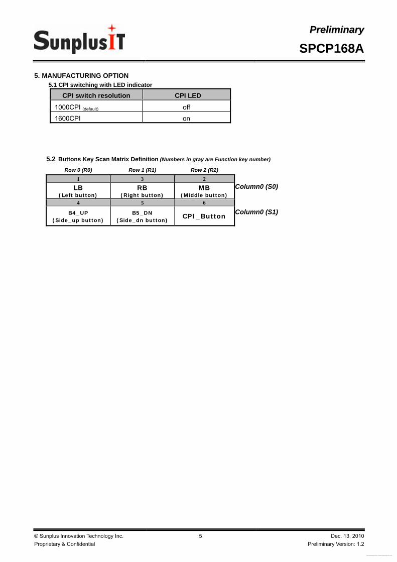
5. MANUFACTURING OPTION 5.1 CPI switching with LED indicator
CPI switch resolution CPI LED
1000CPI (default) off
1600CPI on
5.2 Buttons Key Scan Matrix Definition (Numbers in gray are Function key number)
Row 0 (R0) Row 1 (R1) Row 2 (R2) 1 3 2
LB (Left button)
RB (Right button)
MB (Middle button)
Column0 (S0)
4 5 6
B4_UP (Side_up button)
B5_DN (Side_dn button)
CPI_Button Column0 (S1)
Free Datasheet http://www.Datasheet4U.com

PPrreelliimmiinnaarryy
SPCP168A
© Sunplus Innovation Technology Inc. Proprietary & Confidential
6 Dec. 13, 2010Preliminary Version: 1.2
6. ELECTRICAL CHARACTERISTICS
6.1 Absolute Maximum Ratings
Parameter Symbol Minimum Maximum Units Notes Supply Voltage VDD -0.5 5.5 V Operating Temperature TA -15 55 Storage temperature TS -40 85 Lead Solder temp - - 260 ESD - - 2 KV All pins, human body model Input Voltage VIN -0.5 5.5 V
6.2 Recommend Operating Conditions
Parameter Symbol Minimum Typical Maximum Units Notes Supply Voltage VDD 4.25 5.0 5.25 V Operating Temperature TA 0 - 40 Internal OSC Frequency fCLK - 6.0 - MHz VDD=5V Power Consumption IDD - - TBD mA VDD=5.5V USB Suspend Current ISUSP - - 400 uA VDD=5.25V Low Voltage Detect VLVDZ - 3.6 - V Low Voltage Reset VLVRZ - 3.0 - V
6.3 Optical Navigation Operating Conditions
Parameter Symbol Minimum Typical Maximum Units Notes Distance From lens reference plane to surface Z 2.3 2.4 2.5 mm
Speed S - - 25 In/sec Acceleration A - 0.15 8 G Light level onto IC IRRINC - TBD - MW/m2
λ=639 nm XY_LED Current ILED - 30 - mA @Voltage of XY_LED
= 0.8v
Free Datasheet http://www.Datasheet4U.com

PPrreelliimmiinnaarryy
SPCP168A
© Sunplus Innovation Technology Inc. Proprietary & Confidential
7 Dec. 13, 2010Preliminary Version: 1.2
6.4 DC Electrical Specifications (VDD = 5.0V, Temperature = 25ºC)
Mnemonic Description Item Min. Typ. Max. Unit Condition
VC33 3.3 V regulator output reference VO33 3.0 3.3 3.6 V VDD=5V
VC25 2.5 V regulator output reference VO25 - 2.5 V VDD=5V
Input Voltage High VIH 2.0 - V Input Voltage Low VIL - - 0.8 V DP/CK Output Voltage High VOH 2.8 - 3.6 V Output Voltage Low VOL 0 - 0.3 V Input Voltage High VIH 2.0 - V Input Voltage Low VIL - - 0.8 V Output Voltage High VOH 2.8 - 3.6 V DM/DA Output Voltage Low VOL 0 - 0.3 V USB mode Pull-up RPU 1.20 1.50 1.80 KΩ
Input Voltage High VIH 2.0 - V Input Voltage Low VIL - - 0.8 V VOH =2.2V for ZA/ZB onlyOutput Voltage High VOH 2.2/2.4 - V Source current = 8 mA Output Voltage Low VOL - - 0.5 V Sink current = 8 mA Pull down Resistor RPD 35 50 65 KΩ VIN = VDD Pull up Resistor RPU 10.5 15 19.5 KΩ VIN = VSS
R0 ~ R2 S0 ~ S1 ZA/ZB
RPUP 75 150 225 KΩ All I/O Port Hi-Z Leakage IZ - - 10 µA RP inactive
* The frequency defined in this item is based on the CPU frequency. It is one-half of the oscillation frequency.
6.5 AC Electrical Specifications (VDD = 5.0V, Temperature = 25ºC)
Characteristics Item Min. Typ. Max. Unit Condition Internal Ring oscillator frequency FROSC 1.75 3.5 5.25 KHz Sleep mode delay from no motion to low power
TSLEEP - 1000 - ms
Wakeup delay from sleep mode due to motion
TWUPP - 50 100 ms
Power up delay TPUP - - 50 ms From VDD reach 4.25V until spec’s met
Flashing frequency of LED FLED - 125 - Hz Debounce delay on button input TDBB 5 9 15 ms Z Wheel sampling period TZW 120 200 300 us
Free Datasheet http://www.Datasheet4U.com

PPrreelliimmiinnaarryy
SPCP168A
© Sunplus Innovation Technology Inc. Proprietary & Confidential
8 Dec. 13, 2010Preliminary Version: 1.2
6.6 USB Electrical Specifications (VDD = 5.0V, Temperature = 25ºC)
Characteristics Item Min. Max. Unit Condition Output Signal Crossover Voltage VCRS 1.3 2.0 V CL = 200pF ~ 600pF Input Signal Crossover Voltage VICRS 1.2 2.1 V CL = 200pF ~ 600pF Differential Input Sensitivity VDI 0.2 - V |(D+) – (D-)| See Figure 5 Differential Input Common Mode Range VCM 0.8 2.5 V Include VDI , See Figure 5 Single Ended Receiver Threshold VSE 0.8 2.0 V Transceiver Input Capacitance CIN - 20 pF D+ to VBUS, D- to VBUS
Output High COH 2.8 3.6 V
with 15kΩ to GND and 3.3V internal regulator through 1.5KΩ to D-, See Figure 4
Output Low COH 0 0.3 V
with 15kΩ to GND and 3.3V internal regulator through 1.5KΩ to D-, See Figure 5
Single Ended Output VSED - 0.8 V Input High (Driven) VIH - 2.0 V Input High (Floating) VIHZ 2.7 3.6 V Input Low VIL - 0.5 V
6.7 USB Timing Specifications (VDD = 5.0V, Temperature = 25ºC)
Characteristics Item Min. Max. Unit Condition USB Low-Speed Rise Time / Fall Time TLR/TLF 75 300 ns CL = 200pF ~ 600pF, See
Figure 4
Rise and Fall time matching VLRFM 80 125 % TR/TF; CL = 200pF; Excluding the first transition from the idle time
USB reset time TRESET 8.6 10 us Data Rate tLDRATE 1.4775 1.5225 Mb/s Average bit rate, 1.5Mb/s
+/-1/5% Receiver Jitter Tolerance tDJR1 -75 75 ns To next transition, see Figure
7 Receiver Jitter Tolerance tDJR2 -45 45 ns For paired transition, see
Figure 7 Differential to EOP Transition Skew tLDEOP -40 100 ns See Figure 7 EOP Width at Receiver tLEOPR 670 - ns Accepts EOP, see Figure 7 Source EOP Width tLEOPT 1.25 1.5 us Width of SE0 interval during differential Transition
tLST - 210 ns
Differential Output Jitter tUDJ1 -95 95 ns To next transition, see Figure 8
Differential Output Jitter tUDJ2 -150 150 ns For paired transition, see Figure 8
Free Datasheet http://www.Datasheet4U.com

PPrreelliimmiinnaarryy
SPCP168A
© Sunplus Innovation Technology Inc. Proprietary & Confidential
9 Dec. 13, 2010Preliminary Version: 1.2
Figure 3: Data Signal Rise and Fall Times
Figure 4: Data Signal Voltage Levels
Figure 5: Differential Receiver Input Sensitivity vs. Common Mode Input Range
Free Datasheet ht tp : //www.Datasheet4U.com

PPrreelliimmiinnaarryy
SPCP168A
© Sunplus Innovation Technology Inc. Proprietary & Confidential
10 Dec. 13, 2010Preliminary Version: 1.2
Figure 6: Receiver Jitter Tolerance
Figure 7: Differential to EOP Transition Skew and EOP Width
Figure 8: Differential Output Jitter
Free Datasheet http://www.Datasheet4U.com

PPrreelliimmiinnaarryy
SPCP168A
© Sunplus Innovation Technology Inc. Proprietary & Confidential
11 Dec. 13, 2010Preliminary Version: 1.2
7. FUNCTION BLOCK DESCRIPTION
Please contact SunplusIT sales representatives for more information.
CPU uC
GPIO
Sensor Pixel Array
ZA
VC25
Image Sensor
Power-Down Control
LED Controller XY_LED
internalOscillator
VoltageRegulator
DM/DA
VDD VSS
NavigationEngine
USB / PS2PHY
Power downControl
PLL 24MHz
ZB
VC33
DP/CK
MCU
Optical Navigator
R0 ~ R2S0~S1
Figure 9: Block Diagram
Free Datasheet http://www.Datasheet4U.com
PPrreelliimmiinnaarryy
SPCP168A
© Sunplus Innovation Technology Inc. Proprietary & Confidential
12 Dec. 13, 2010Preliminary Version: 1.2
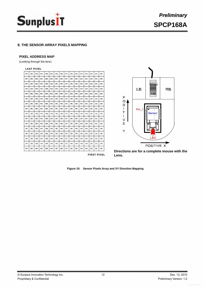
8. THE SENSOR ARRAY PIXELS MAPPING
000102030405060708090A0B0C0D0E0F
101112131415161718191A1B1C1D1E1F
202122232425262728292A2B2C2D2E2F
303132333435363738393A3B3C3D3E3F
404142434445464748494A4B4C4D4E4F
505152535455565758595A5B5C5D5E5F
606162636465666768696A6B6C6D6E6F
707172737475767778797A7B7C7D7E7F
808182838485868788898A8B8C8D8E8F
909192939495969798999A9B9C9D9E9F
A0A1A2A3A4A5A6A7A8A9AAABACADAEAF
B0B1B2B3B4B5B6B7B8B9BABBBCBDBEBF
C0C1C2C3C4C5C6C7C8C9CACBCCCDCECF
D0D1D2D3D4D5D6D7D8D9DADBDCDDDEDF
E0E1E2E3E4E5E6E7E8E9EAEBECEDEEEF
F0F1F2F3F4F5F6F7F8F9FAFBFCFDFEFF
LAST PIXEL
FIRST PIXEL
PIXEL ADDRESS MAP(Looking through the lens)
Directions are for a complete mouse with the Lens.
Figure 10: Sensor Pixels Array and XY Direction Mapping
Free Datasheet http://www.Datasheet4U.com

PPrreelliimmiinnaarryy
SPCP168A
© Sunplus Innovation Technology Inc. Proprietary & Confidential
13 Dec. 13, 2010Preliminary Version: 1.2
9. APPLICATION CIRCUIT EXAMPLE FOR SPCP168A
B4
R151 ohm
VCC
B5
D+/CLK
C40.1uF
R1
SPCP168A
U1
SPCP168A
21110
8
3
7
12
5
13
4
9
6
114
R0S1S0
VSS
DM
VC33
ZB
VD
D
ZA
DP
XY_LED
VC25
R1R2Closed to Conn #
R0
D-/DATA
R2
C6100pF
C14.7 uF
12
C6, C7 for USB /EMI complianced
S1
R0
C310uF
12Buttons Matrix
S2
Closed to Chip
Z Axis
SW1Z Encoder
231
C510uF
12
C20.1uF
S1
S3
MB
# Not Mounted
C7100pF
VCC
S0
S5
VCC
GND
LED ED80LD1
12
RB
S0
Surface
JP1
USB/PS2 CONN
12345
R1
S1
Closed to Chip
ESDR2
S4LB
#
Figure11: SPCP168A – 5 Buttons Wheel Mouse SoC application circuitry (Generic)
VCC
JP1
USB/PS2 CONN
12345
CPI
GND
LED ED80
RB
R1
Surface
LD1
12
S1
R151 ohm
Closed to Chip
LB
VCC
R2
S6
#
S1
B4
ESD
S0
R0
C40.1uF
SPCP168A
U1
SPCP168A
21110
8
3
7
12
5
13
4
9
6
114
R0S1S0
VSS
DM
VC33
ZB
VD
D
ZA
DP
XY_LED
VC25
R1R2
Closed to Chip
B5
D+/CLK
C6100pF
#Closed to Conn
C14.7 uF
12
D-/DATA
S0
R2
R1
C310uF
12
S2
S4
C6, C7 for USB /EMI complianced
SW1Z Encoder
231
C510uF
12
Buttons Matrix
S1
C20.1uF
R0
S3
C7100pF
Z Axis
VCC
S5
MB
# Not Mounted
Figure 12: SPCP168A – 5 Buttons Wheel Mouse SoC with CPI switch application circuitry (none CPI LED)
Free Datasheet http://www.Datasheet4U.com

PPrreelliimmiinnaarryy
SPCP168A
© Sunplus Innovation Technology Inc. Proprietary & Confidential
14 Dec. 13, 2010Preliminary Version: 1.2
C310uF
12
S5
Closed to Chip
# Not Mounted
R1
CPI
Z Axis
Closed to Chip
#
C20.1uF
R2
GND
S1R3
2K ohm
R0
C510uF
12
R2470
S6
ESD
S0
Surface
C7100pF
R151 ohm
S0
S1
#
S3
CPI LED
D-/DATA
R0
VCC
R1
R0
JP1
USB/PS2 CONN
12345
B4
B5
SPCP168A
U1
SPCP168A
21110
8
3
7
12
5
13
4
9
6
114
R0S1S0
VSS
DM
VC33
ZB
VD
D
ZA
DP
XY_LED
VC25
R1R2
LD2CPI_1
12
S2
C40.1uF
RB
VCC
S1
LD1
12
C6100pF
LB
Buttons Matrix
D+/CLK
LED ED80
S4
C6, C7 for USB /EMI complianced
VCC
MB
C14.7 uF
12
R2
SW1Z Encoder
231
Closed to Conn
Figure 13: SPCP168A - 5Buttons Wheel Mouse SoC with CPI and LED application circuitry
Closed to Chip
D+/CLK
S0Buttons Matrix
C7100pF
R0
LD1
12
C6, C7 for USB /EMI complianced
S2
S3
JP1
USB/PS2 CONN
12345
Surface
VCC
# Not Mounted
VCC
C20.1uF
R2
##Closed to Conn
R1
S1
SPCP168A
U1
SPCP168A
21110
8
3
7
12
5
13
4
9
6
114
R0S1S0
VSS
DM
VC33
ZB
VD
D
ZA
DP
XY_LED
VC25
R1R2
RB
Z Axis
S0
GND
LED ED80
C14.7 uF
12
C510uF
12
SW1Z Encoder
231
R151 ohm
D-/DATA
R0
VCC
LB
C40.1uF
ESD
C310uF
12
R2
Closed to Chip
C6100pF
R1
MB
Figure 14: SPCP168A – 3 Buttons Wheel Mouse SoC application circuitry (Generic)
Free Datasheet http://www.Datasheet4U.com

PPrreelliimmiinnaarryy
SPCP168A
© Sunplus Innovation Technology Inc. Proprietary & Confidential
15 Dec. 13, 2010Preliminary Version: 1.2
D+/CLK
VCC
C20.1uF
VCC
S3
Z Axis
C40.1uFButtons Matrix
#
R151 ohm
#
S0
LD1
12
SPCP168A
U1
SPCP168A
21110
8
3
7
12
5
13
4
9
6
114
R0S1S0
VSS
DM
VC33
ZB
VD
D
ZA
DP
XY_LED
VC25
R1R2
CPI
JP1
USB/PS2 CONN
12345
C14.7 uF
12
GNDClosed to Conn
S1
S0
R1
C6100pF
LB
R2
RB
Closed to Chip
SW1Z Encoder
231
S2
S1
R0
S1
VCC
# Not Mounted
R1
D-/DATA
C7100pF
ESD
R2
R0
C510uF
12
S6
MB
C6, C7 for USB /EMI complianced C310uF
12
Closed to Chip
Surface
LED ED80
Figure 15: SPCP168A – 3 Buttons Wheel Mouse SoC with CPI switch application circuitry (none CPI LED)
R0ESD Closed to Conn
Buttons Matrix
Z Axis
# Not Mounted
SW1Z Encoder
231
VCCClosed to Chip
C40.1uF
C14.7 uF
12
SPCP168A
U1
SPCP168A
21110
8
3
7
12
5
13
4
9
6
114
R0S1S0
VSS
DM
VC33
ZB
VD
D
ZA
DP
XY_LED
VC25
R1R2
LD1
12
LB
R2
CPI
C6, C7 for USB /EMI complianced
R151 ohm
S1
S2
C510uF
12
C6100pF
D-/DATA
R1S3
R1#
Surface
R0
LED ED80
CPI LED
C20.1uF
C310uF
12
R2
GND#
JP1
USB/PS2 CONN
12345
S1
R0
R3
2K ohm
D+/CLK
MB
S0
LD2CPI_1
12
VCC
Closed to Chip
S6
C7100pF S0
VCC
RB
S1
R2470
Figure 16: SPCP168A – 3 Buttons Wheel Mouse SoC with CPI and LED application circuitry
Free Datasheet http://www.Datasheet4U.com

PPrreelliimmiinnaarryy
SPCP168A
© Sunplus Innovation Technology Inc. Proprietary & Confidential
16 Dec. 13, 2010Preliminary Version: 1.2
10. EMI Test Summary Reference 10.1 DUT sample photo
Top Side Bottom Side
DUT test Circuitry is based on figure 14 schematic manufactured
Free Datasheet http://www.Datasheet4U.com

PPrreelliimmiinnaarryy
SPCP168A
© Sunplus Innovation Technology Inc. Proprietary & Confidential
17 Dec. 13, 2010Preliminary Version: 1.2
Note: under test criteria -3dB; Passed CE / FCC test requirement
Shenzhen new kam hon electronic technology Co., LTD
TEL:+86-0755-82565136
FAX:+86-0755-82565136
Phone:13670234576
Emila:[email protected]
Free Datasheet http://www.Datasheet4U.com

PPrreelliimmiinnaarryy
SPCP168A
© Sunplus Innovation Technology Inc. Proprietary & Confidential
18 Dec. 13, 2010Preliminary Version: 1.2
10.3 SPCP168A EMI Test Summary (Vertical)
Note: under test criteria -3dB; Passed CE / FCC test requirement
Shenzhen new kam hon electronic technology Co., LTD
TEL:+86-0755-82565136
FAX:+86-0755-82565136
Phone:13670234576
Emila:[email protected]
Free Datasheet http://www.Datasheet4U.com

PPrreelliimmiinnaarryy
SPCP168A
© Sunplus Innovation Technology Inc. Proprietary & Confidential
19 Dec. 13, 2010Preliminary Version: 1.2
11 PACKAGE
11.1 SPCP168A 14Pin Package Dimension
Free Datasheet http://www.Datasheet4U.com

PPrreelliimmiinnaarryy
SPCP168A
© Sunplus Innovation Technology Inc. Proprietary & Confidential
20 Dec. 13, 2010Preliminary Version: 1.2
11.2 Ordering Information
Product Number Package Type
SPCP168A –HR033 Package form - PDIP14 Notes: 1.) If needs code programming service, please contact with SunplusIT sales representatives for more information 2.) Above ordering information are for the green packages (default) only
12. DISCLAIMER The information appearing in this publication is believed to be accurate.
Integrated circuits sold by Sunplus Innovation Technology are covered by the warranty and patent indemnification provisions stipulated in
the terms of sale only. SUNPLUSIT makes no warranty, expressed, statutory implied or by description regarding the information in this
publication or regarding the freedom of the described chip(s) from patent infringement. FURTHERMORE, SUNPLUSIT MAKES NO
WARRANTY OF MERCHANTABILITY OR FITNESS FOR ANY PURPOSE. SUNPLUSIT reserves the right to halt production or alter the
specifications and prices at any time without notice. Accordingly, the reader is cautioned to verify that the data sheets and other information
in this publication are current before placing orders. Products described herein are intended for use in normal commercial applications.
Applications involving unusual environmental or reliability requirements, e.g. military equipment or medical life support equipment, are
specifically not recommended without additional processing by SUNPLUSIT for such applications. Please note that application circuits
illustrated in this document are for reference purposes only.
13. REVISION HISTORY
Date Revision # Description Page
DEC. 13, 2010 1.2 Revised application circuitry
Added EMI test summary
13 ~15
16 ~18
JUL. 31, 2010 1.1 Revised application circuitry 13 ~15
MAY. 31, 2010 1.0 Original 17
Free Datasheet http://www.Datasheet4U.com


