Data Remanence in Semiconductor Devices Introduction
16
Data Remanence in Semiconductor Devices Peter Gutmann IBM T.J.Watson Research Center Introduction 1996: Securely deleting data from magnetic media is hard 2001: Semiconductors aren’t so easy either Magnetic media • Relatively simple solution • Light technical background coverage Semiconductors • Many different, nontrivial solutions • Lots of technical background coverage
Transcript of Data Remanence in Semiconductor Devices Introduction

Data Remanence in Semiconductor Devices
Peter Gutmann
IBM T.J.Watson Research Center
Introduction
1996: Securely deleting data from magnetic media is hard
2001: Semiconductors aren’t so easy either
Magnetic media• Relatively simple solution• Light technical background coverage
Semiconductors• Many different, nontrivial solutions• Lots of technical background coverage
Existing Work on Semiconductor Forensics
Semiconductor Device Physics
Electrons exist in discrete energy bands
Applying energy moves electrons from valence to conduction band
Electronenergy Band gap
Conductionband
Valenceband
Bands• Are too far apart in insulators• Touch or overlap in conductors• Conduction occurs via electrons or holes (but not both) in
semiconductors

Semiconductor Device Physics (ctd)
Semiconductor types• p-type conducts by holes• n-type conducts by electrons
P-N junction diode• Conducts when forward
biased (p-type at +ve)• Doesn’t conduct when
reverse biased• Exact mechanism is fairly
complex
n-type
p-type
Passivationlayer
Ohmiccontact
Semiconductor Device Physics (ctd)
n-channel MOSFET• Applying voltage to gate
forms conducting electron inversion layer beneath it
• Current flows from source to drain
p-type substraten-type n-type
Passivationlayer
Ohmiccontact
DrainGate
Source
Device types• n-channel devices move electrons (fast)• p-channel devices move holes (slower)• Complementary MOS (CMOS) uses both types
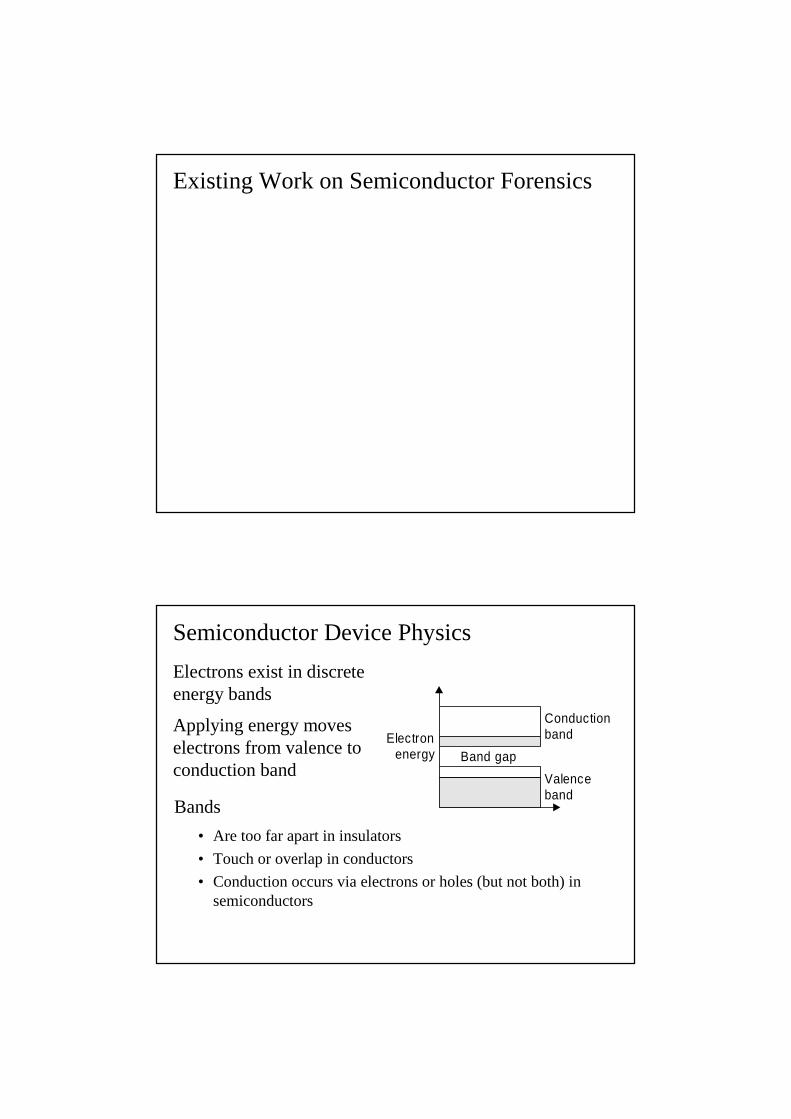
Semiconductor MemoriesStatic RAM
• Value written via Data/Data stored in cross-coupled flip-flops• Individually addressable cells
L L Loaddevices
+V
SelectSelect
DataData
Semiconductor Memories (ctd)
Dynamic RAM
• Capacitor for storage, transistor for read/write/refresh• Sense amplifiers compare cell voltage to value in reference cell• Cells use various exotic techniques to shrink size but keep
capacitor storage constant
Data
Select
Storagecapacitor

Electromigration
Relocation of metal atoms due to collision with electrons• Electron wind• Material removed to create voids at negative electrode• Material deposited to create hillocks/whiskers at positive
electrode
Some (minimal) healing occurs due to backflow when stress is removed
Electromigration (ctd)
Imag
e co
urte
sy D
r.V-C
.Lo

Electromigration (ctd)
Imag
e co
urte
sy D
r.V-C
.Lo
Electromigration (ctd)
Alloys are used to combat electromigration• Cu in Al• Sn in Cu
Cu or Sn solute atoms are displaced until the conductor behaves like the original pure metal• Can be detected using electron microprobing techniques

Hot Carriers
MOSFETs have very small device dimensions → high electric fields (MV/cm)• Electrons are accelerated to high speeds (hot carriers)
• Can tunnel into gate oxide– Detrapping time = nanoseconds … days
• Can tunnel into passivation layer– Permanent
p-type substraten-type n-type
Passivationlayer
Ohmiccontact
DrainGate
Source
Hot Carrier Effects
Excess charge reduces on-state current (n-MOS), off-state current (p-MOS)• Change of several hundred mV of memory cell voltage over a
few minutes• Writing 1 over 0 leads to a drop in cell threshold voltage• Writing 0 over 1 leads to an increase in cell threshold voltage
Detectable by changing the setting of the reference cell
Affects logic circuits in general• Changes currents, voltages, capacitance for the device

Ionic Contamination
Most common are sodium and to a lesser extent potassium• Sodium ions have a high mobility in silicon• Migrate towards Si/SiO2 interface• Reduce threshold voltage of n-MOS, increase it for p-MOS• Detectable using the same techniques used for hot carriers• Addressed using passivation layers
Reliability studies indicate this only occurs at random locations where impurities have penetrated the passivation layer(s)• Improved manufacturing techniques have mostly eliminated
this avenue for data recovery
Other Effects
Radiation-induced charging can affect MOSFET turn-on voltage• Can be used to affect voltage thresholds, timings, power supply
and leakage currents• Freeze a device to prevent a change on logic state• Lock out tamper-responding circuitry (eg erase-on-tamper)• High-end crypto devices include sensors to detect ionising
radiation

Semiconductor Forensic Techniques
Wide variety of techniques in use for semiconductor testing• No-one can agree on which parameters to measure• Many results are obtained for specially-created test structures• Large variety of devices in use
Some of the more common techniques• IDDQ testing (measure device current consumption, fully on or
off MOSFETs have low IDDQ)• Vary operating voltage and temperature to test for hot carrier
effects• Measure substrate current, gate current, current in gated drain-
substrate diode, etc etc• Many tools and journals cover this topic
Semiconductor Forensic Techniques (ctd)
Probing techniques• Design for test (DFT) allows test access• Mechanical probing• Deep submicron testing requires the use of focused ion beam
(FIB) techniques to– Expose buried conductors– Deposit new probe points
• Used by Chipworks to rebuild ATMEL EEPROM from aircraft black box

Avoiding Short-term Data Retention
Don’t store the same value for more than a few minutes• Test of SRAM devices
found changes in threshold voltage, transconductance, drain-source current after 100-500s stress
• Reads and writes of 0 and 1 bits stress different access transistors
L L Loaddevices
+V
SelectSelect
DataData
Avoiding Short-term Data Retention (ctd)
SRAM burn-in was a problem in the 1980s• DES master keys stored in security modules were recovered
almost intact on power-up
Far less likely with current devices• 1½ hours at 75°C• 3 days at 50°C• 2 months at 20°C• 3 years at 0°C
Periodically flip bits to avoid data retention effects• Can be implemented automatically as part of DRAM refresh
cycle

Avoiding Long-term Data Retention
Crypto processors/accelerators repeatedly feed a private key through the same circuits• Zeroising electromigration/hot-carrier effects is hard
Process dummy data when circuits are idle• Very complex to implement• High-use circuits which exhibit problems are never idle• Low-use circuits don’t exhibit problems
Avoiding Long-term Data Retention (ctd)
Virtually all Feistel ciphers/hashes iterate one round multiple times
Bignum units also typically iterate using 512- or 1024-bit adders and shift registers• 1024-bit multiply uses 1k adds• 1024-bit modmult uses 1k multiplies• 1M applications of the same cryptovariable per RSA op
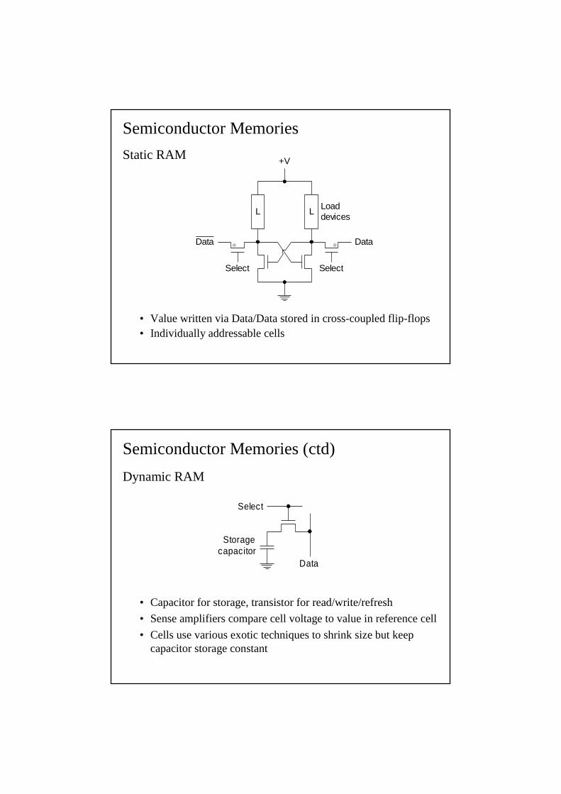
EEPROM Memory Cells
MOSFET with an extra, floating gate
Older FLOTOX cells used Fowler-Nordheim tunneling to tunnel electrons into/out of the floating gate
• Stored charge changes threshold voltage by 3-3.5V for 5V cell
N+ N+P-substrate
DrainSource
Tunneloxide
Gateoxide
GateFloating
gate
eee
eeeeeeee
eeeeeeee
Gate at+ve
Gateat gnd
Gate
Gate o
xide
Drain
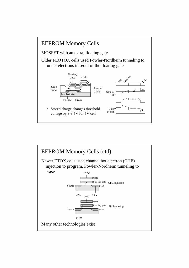
EEPROM Memory Cells (ctd)
Newer ETOX cells used channel hot electron (CHE) injection to program, Fowler-Nordheim tunneling to erase
Many other technologies exist
DrainSource
G ate
F loa ting ga te
+12V
+~6VGND
DrainSource
G ate
F loa ting ga te
GND
+12V
CHE Injection
FN Tunneling

EEPROM Memory Cells (ctd)
To increase storage density, one select transistor controls many cells• Erase is done on groups of cells
Some cells erase faster/slower than others• Keep repeating erase process until all cells read back as erased
– Programming is also done speculatively• Problems with overprogrammed/overerased cells
Flash Memory
Most common is NAND flash, multiple cells controlled by a single select transistor
• Typically move data 64-256 bytes at a time• As with EEPROM, many different technologies in use
Bit lineSelect gate (source)
W ord line 1
W ord line 2
W ord line 3
W ord line 4
Select gate (drain)
Data Remanence in EEPROM/Flash
Floating gate slowly accumulates electrons• Typical cell can handle 1M program/erase cycles• Whole collection can handle 10k-100k cycles• Cycle device until memory cells freeze in programmed state
– Challenge/response mechanisms for smart cards– Card RNG ends up in all-ones state
Trapped charge can be determined by measuring gate-induced drain leakage (GIDL) current
Older devices tied read reference voltage to supply voltage• Can determine cell threshold by varying supply voltage• Can also alter programmed/erased status this way
Data Remanence in EEPROM/Flash (ctd)
Programming Disturbs• Shared circuitry can cause program/erase to leak over into
adjacent cells– Drain/bitline disturbs– Gate/wordline disturbs– Read disturbs
Various other problems shared with RAM cells
Large threshold shift in virgin cells after first program-and-erase cycle• Can differentiate between erased and never-programmed cells

Data Remanence in EEPROM/Flash (ctd)
Overerasing (re-erase of already-erased cells) leaves floating gate positively charged• Memory transistor becomes depletion-mode transistor• Some devices first program the cells before erasing them
As with hard drives, EEPROM/flash often maps out failing sectors• Unlike hard drives, the designers definitely know that sectors
will fail eventually and design around it
Data Remanence in EEPROM/Flash (ctd)
Flash filesystems use wear-leveling techniques to avoid overuse of groups of cells• Log-structured filesystem• Trying to perform n overwrite passes will simply write n fresh
copies• No easy solution to this problem unless it’s possible to modify
the filesystem code
Some devices store data in staging areas to implement program-without-erase mode• Original data can be recovered from memory cells, new data
from staging area• Causes problems for erase-on-tamper if the update doesn’t
complete fully

Recommendations
Don’t store cryptovariables for long periods in the same location
Don’t store cryptovariables in plaintext form in nonvolatile memory
Cycle EEPROM/flash cells 10-100 times before using them
Don’t assume that a key held in RAM has been destroyed when the RAM is cleared
Design devices to avoid repeatedly running the same signals over dedicated data lines
Beware of too-intelligent nonvolatile memory devices