
DAC5675-EP (Rev. A) - TI · The DAC5675 comprises a low-voltagedifferential signaling ......
28
www.ti.com FEATURES APPLICATIONS DESCRIPTION/ORDERING INFORMATION DAC5675-EP SGLS381A – OCTOBER 2006 – REVISED OCTOBER 2006 14-Bit 400-MSPS Digital-to-Analog Converter • Power Dissipation: 660 mW at f CLK = 400 MSPS, f OUT = 20 MHz • 400-MSPS Update Rate • Package: 48-Pin PowerPAD™ • Controlled Baseline Thermally-Enhanced Thin Quad Flat Pack – One Assembly (HTQFP) T JA = 29.1°C/W – One Test Site – One Fabrication Site • Extended Temperature Performance of –55°C • Cellular Base Transceiver Station Transmit to 125°C Channel: – CDMA: WCDMA, CDMA2000, IS-95 • Enhanced Diminishing Manufacturing Sources (DMS) Support – TDMA: GSM, IS-136, EDGE/GPRS – Supports Single-Carrier and Multicarrier • Enhanced Product-Change Notification Applications • LVDS-Compatible Input Interface • Test and Measurement: Arbitrary Waveform • Spurious-Free Dynamic Range (SFDR) to Generation Nyquist • Military Communications – 69 dBc at 70 MHz IF, 400 MSPS • W-CDMA Adjacent Channel Power Ratio (ACPR) – 73 dBc at 30.72-MHz IF, 122.88 MSPS – 71 dBc at 61.44-MHz IF, 245.76 MSPS • Differential Scalable Current Outputs: 2 mA to 20 mA • On-Chip 1.2-V Reference • Single 3.3-V Supply Operation The DAC5675 is a 14-bit resolution high-speed digital-to-analog converter (DAC). The DAC5675 is designed for high-speed digital data transmission in wired and wireless communication systems, high-frequency direct-digital synthesis (DDS), and waveform reconstruction in test and measurement applications. The DAC5675 has excellent spurious-free dynamic range (SFDR) at high intermediate frequencies, which makes it well-suited for multicarrier transmission in TDMA- and CDMA-based cellular base transceiver stations (BTSs). The DAC5675 operates from a single-supply voltage of 3.3 V. Power dissipation is 660 mW at f CLK = 400 MSPS, f OUT = 70 MHz. The DAC5675 provides a nominal full-scale differential current output of 20 mA, supporting both single-ended and differential applications. The output current can be directly fed to the load with no additional external output buffer required. The output is referred to the analog supply voltage AV DD . The DAC5675 comprises a low-voltage differential signaling (LVDS) interface for high-speed digital data input. LVDS features a low differential voltage swing with a low constant power consumption across frequency, allowing for high-speed data transmission with low noise levels; that is, with low electromagnetic interference (EMI). LVDS is typically implemented in low-voltage digital CMOS processes, making it the ideal technology for high-speed interfacing between the DAC5675 and high-speed low-voltage CMOS ASICs or FPGAs. The DAC5675 current-source-array architecture supports update rates of up to 400 MSPS. On-chip edge-triggered input latches provide for minimum setup and hold times, thereby relaxing interface timing. Please be aware that an important notice concerning availability, standard warranty, and use in critical applications of Texas Instruments semiconductor products and disclaimers thereto appears at the end of this data sheet. PowerPAD is a trademark of Texas Instruments. PRODUCTION DATA information is current as of publication date. Copyright © 2006, Texas Instruments Incorporated Products conform to specifications per the terms of the Texas Instruments standard warranty. Production processing does not necessarily include testing of all parameters.
Transcript of DAC5675-EP (Rev. A) - TI · The DAC5675 comprises a low-voltagedifferential signaling ......
www.ti.com
FEATURES
APPLICATIONS
DESCRIPTION/ORDERING INFORMATION
DAC5675-EP
SGLS381A–OCTOBER 2006–REVISED OCTOBER 2006
14-Bit 400-MSPS Digital-to-Analog Converter
• Power Dissipation: 660 mW atfCLK = 400 MSPS, fOUT = 20 MHz• 400-MSPS Update Rate
• Package: 48-Pin PowerPAD™• Controlled BaselineThermally-Enhanced Thin Quad Flat Pack– One Assembly(HTQFP) TJA = 29.1°C/W
– One Test Site– One Fabrication Site
• Extended Temperature Performance of –55°C • Cellular Base Transceiver Station Transmitto 125°C Channel:
– CDMA: WCDMA, CDMA2000, IS-95• Enhanced Diminishing ManufacturingSources (DMS) Support – TDMA: GSM, IS-136, EDGE/GPRS
– Supports Single-Carrier and Multicarrier• Enhanced Product-Change NotificationApplications• LVDS-Compatible Input Interface
• Test and Measurement: Arbitrary Waveform• Spurious-Free Dynamic Range (SFDR) toGenerationNyquist
• Military Communications– 69 dBc at 70 MHz IF, 400 MSPS
• W-CDMA Adjacent Channel Power Ratio(ACPR)– 73 dBc at 30.72-MHz IF, 122.88 MSPS– 71 dBc at 61.44-MHz IF, 245.76 MSPS
• Differential Scalable Current Outputs: 2 mAto 20 mA
• On-Chip 1.2-V Reference• Single 3.3-V Supply Operation
The DAC5675 is a 14-bit resolution high-speed digital-to-analog converter (DAC). The DAC5675 is designed forhigh-speed digital data transmission in wired and wireless communication systems, high-frequency direct-digitalsynthesis (DDS), and waveform reconstruction in test and measurement applications. The DAC5675 hasexcellent spurious-free dynamic range (SFDR) at high intermediate frequencies, which makes it well-suited formulticarrier transmission in TDMA- and CDMA-based cellular base transceiver stations (BTSs).
The DAC5675 operates from a single-supply voltage of 3.3 V. Power dissipation is 660 mW atfCLK = 400 MSPS, fOUT = 70 MHz. The DAC5675 provides a nominal full-scale differential current output of 20mA, supporting both single-ended and differential applications. The output current can be directly fed to the loadwith no additional external output buffer required. The output is referred to the analog supply voltage AVDD.
The DAC5675 comprises a low-voltage differential signaling (LVDS) interface for high-speed digital data input.LVDS features a low differential voltage swing with a low constant power consumption across frequency,allowing for high-speed data transmission with low noise levels; that is, with low electromagnetic interference(EMI). LVDS is typically implemented in low-voltage digital CMOS processes, making it the ideal technology forhigh-speed interfacing between the DAC5675 and high-speed low-voltage CMOS ASICs or FPGAs. TheDAC5675 current-source-array architecture supports update rates of up to 400 MSPS. On-chip edge-triggeredinput latches provide for minimum setup and hold times, thereby relaxing interface timing.
Please be aware that an important notice concerning availability, standard warranty, and use in critical applications of TexasInstruments semiconductor products and disclaimers thereto appears at the end of this data sheet.
PowerPAD is a trademark of Texas Instruments.
PRODUCTION DATA information is current as of publication date. Copyright © 2006, Texas Instruments IncorporatedProducts conform to specifications per the terms of the TexasInstruments standard warranty. Production processing does notnecessarily include testing of all parameters.
www.ti.com
DAC5675-EP
SGLS381A–OCTOBER 2006–REVISED OCTOBER 2006
The DAC5675 has been specifically designed for a differential transformer-coupled output with a 50-Ωdoubly-terminated load. With the 20-mA full-scale output current, both a 4:1 impedance ratio (resulting in anoutput power of 4 dBm) and 1:1 impedance ratio transformer (–2 dBm) is supported. The last configuration ispreferred for optimum performance at high output frequencies and update rates. The outputs are terminated toAVDD and have voltage compliance ranges from AVDD – 1 to AVDD + 0.3 V.
An accurate on-chip 1.2-V temperature-compensated bandgap reference and control amplifier allows the user toadjust this output current from 20 mA down to 2 mA. This provides 20-dB gain range control capabilities.Alternatively, an external reference voltage may be applied. The DAC5675 features a SLEEP mode, whichreduces the standby power to approximately 18 mW.
The DAC5675 is available in a 48-pin PowerPAD™ thermally-enhanced thin quad flat pack (HTQFP). Thispackage increases thermal efficiency in a standard size IC package. The device is specified for operation overthe military temperature range of –55°C to 125°C.
This integrated circuit can be damaged by ESD. Texas Instruments recommends that all integrated circuits be handled withappropriate precautions. Failure to observe proper handling and installation procedures can cause damage.
ESD damage can range from subtle performance degradation to complete device failure. Precision integrated circuits may bemore susceptible to damage because very small parametric changes could cause the device not to meet its publishedspecifications.
ORDERING INFORMATION (1)
PACKAGE PACKAGE PACKAGE ORDERING TRANSPORTPRODUCT LEAD DESIGNATOR MARKING NUMBER MEDIA, QUANTITY
DAC5675MPHPREP Tape and reel, 1000DAC5675-EP 48 HTQFP PHP DAC5675-EP
DAC5675MPHPEP Tray, 250
(1) For the most current package and ordering information, see the Package Option Addendum located at the end of this data sheet.
TQFP-48 PACKAGE THERMAL CHARACTERISTICS
SAME PACKAGE PowerPADPARAMETER FORM WITHOUT CONNECTED TO
PowerPAD PCB THERMAL PLANE (1)
RθJA Thermal resistance, junction to ambient (1) (2) 108.71°C/W 29.11°C/W
RθJC Thermal resistance, junction to case (1) (2) 18.18°C/W 1.14°C/W
(1) Airflow is at 0 LFM (no airflow).(2) Specified with the PowerPAD bond pad on the backside of the package soldered to a 2-oz CU plate PCB thermal plane
2 Submit Documentation Feedback
www.ti.com
Bandgap
Reference
1.2V
Control Amp
Current
Source
Array
Output
Current
Switches
DAC
Latch
+
Drivers
DecoderInput
Latches
LVDS
Input
Interface
Clock Distribution
SLEEP
EXTIO
BIASJ
D[13:0]A
D[13:0]B
CLK
CLKC
AVDD(4x) AGND(4x) DVDD(2x) DGND(2x)
14
14
DAC5675-EP
DAC5675-EP
SGLS381A–OCTOBER 2006–REVISED OCTOBER 2006
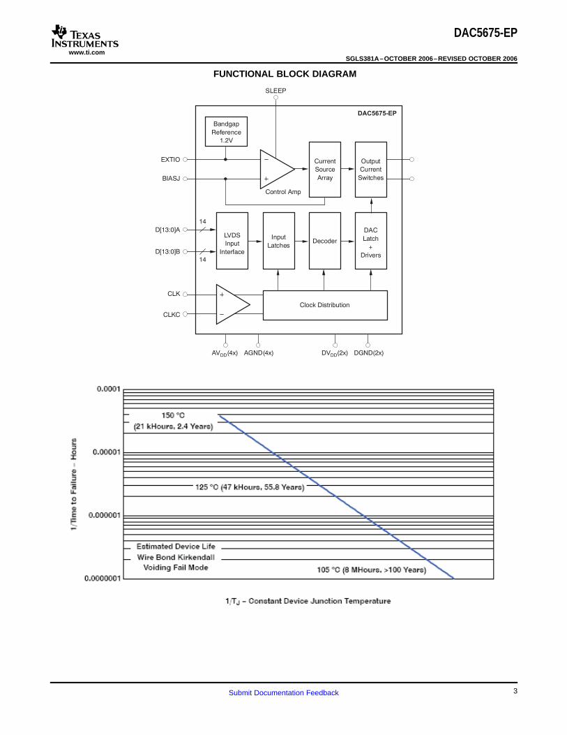
FUNCTIONAL BLOCK DIAGRAM
3Submit Documentation Feedback
www.ti.com
Absolute Maximum Ratings
DAC5675-EP
SGLS381A–OCTOBER 2006–REVISED OCTOBER 2006
over operating free-air temperature range (unless otherwise noted) (1)
DAC5675-EP UNIT
AVDD(2) –0.3 to 3.6
Supply voltage range DVDD(3) –0.3 to 3.6 V
AVDD to DVDD –3.6 to 3.6
Voltage between AGND and DGND –0.3 to 0.5 V
CLK, CLKC (2) –0.3 to AVDD + 0.3 V
Digital input D[13:0]A, D[13:0]B (3), SLEEP, DLLOFF –0.3 to DVDD + 0.3 V
IOUT1, IOUT2 (2) –1 to AVDD + 0.3 V
EXTIO, BIASJ (2) –1 to AVDD + 0.3 V
Peak input current (any input) 20 mA
Peak total input current (all inputs) –30 mA
Operating free-air temperature range, TA –55 to 125 °C
Storage temperature range –65 to 150 °C
Lead temperature 1,6 mm (1/16 in) from the case for 10 s 260 °C
(1) Stresses above those listed under Absolute Maximum Ratings may cause permanent damage to the device. Exposure to absolutemaximum conditions for extended periods may degrade device reliability. These are stress ratings only, and functional operation of thedevice at these or any other conditions beyond those indicated under recommended operating conditions is not implied. Exposure toabsolute-maximum-rated conditions for extended periods may affect device reliability.
(2) Measured with respect to AGND(3) Measured with respect to DGND
4 Submit Documentation Feedback

www.ti.com
DC Electrical Characteristics
DAC5675-EP
SGLS381A–OCTOBER 2006–REVISED OCTOBER 2006
over operating free-air temperature range, typical values at 25°C, AVDD = 3.3 V, DVDD = 3.3 V, IO(FS) = 20 mA (unlessotherwise noted)
PARAMETER TEST CONDITIONS MIN TYP MAX UNIT
Resolution 14 Bit
DC Accuracy (1)
INL Integral nonlinearity –4 ±1.5 4.6 LSBTMIN to TMAX
DNL Differential nonlinearity –2 ±0.6 2.2 LSB
Monotonicity Monotonic 12b Level
Analog Output
IO(FS) Full-scale output current 2 20 mA
AVDD = 3.15 V to 3.45 V,Output compliance range AVDD – 1 AVDD + 0.3 VIO(FS) = 20 mA
Offset error 0.01 %FSR
Without internal reference –10 5 10Gain error %FSR
With internal reference –10 2.5 10
Output resistance 300 kΩ
Output capacitance 5 pF
Reference Output
V(EXTIO) Reference voltage 1.17 1.23 1.29 V
Reference output current (2) 100 nA
Reference Input
V(EXTIO) Input reference voltage 0.6 1.2 1.25 V
Input resistance 1 MΩ
Small-signal bandwidth 1.4 MHz
Input capacitance 100 pF
Temperature Coefficients
Offset drift 12 ppm of FSR/°C
∆V(EXTIO) Reference voltage drift ±50 ppm/°C
Power Supply
AVDD Analog supply voltage 3.15 3.3 3.6 V
DVDD Digital supply voltage 3.15 3.3 3.6 V
I(AVDD) Analog supply current (3) 115 mA
I(DVDD) Digital supply current (3) 85 mA
Sleep mode 18PD Power dissipation mW
AVDD = 3.3 V, DVDD = 3.3 V 660 900
APSRR –0.9 ±0.1 0.9Analog and digital AVDD = 3.15 V to 3.45 V %FSR/Vpower-supply rejection ratioDPSRR –0.9 ±0.1 0.9
(1) Measured differential at IOUT1 and IOUT2: 25 Ω to AVDD(2) Use an external buffer amplifier with high impedance input to drive any external load.(3) Measured at fCLK = 400 MSPS and fOUT = 70 MHz
5Submit Documentation Feedback

www.ti.com
AC Electrical Characteristics
DAC5675-EP
SGLS381A–OCTOBER 2006–REVISED OCTOBER 2006
over operating free-air temperature range, typical values at 25°C, AVDD = 3.3 V, DVDD = 3.3 V, IO(FS) = 20 mA, differentialtransformer-coupled output, 50-Ω doubly-terminated load (unless otherwise noted)
PARAMETER TEST CONDITIONS MIN TYP MAX UNIT
Analog Output
fCLK Output update rate 400 MSPS
ts(DAC) Output setting time to 0.1% Transition: code x2000 to x23FF 12 ns
tPD Output propagation delay 1 ns
tr(IOUT) Output rise time, 10% to 90% 2 ns
tf(IOUT) Output fall time, 90% to 10% 2 ns
IOUTFS = 20 mA 55Output noise pA/√Hz
IOUTFS = 2 mA 30
AC Linearity
fCLK = 100 MSPS, fOUT = 19.9 MHz 73
fCLK = 160 MSPS, fOUT = 41 MHz 72
fCLK = 200 MSPS, fOUT = 70 MHz 68THD Total harmonic distortion dBc
fOUT = 20.1 MHz 72
fCLK = 400 MSPS fOUT = 70 MHz 71
fOUT = 140 MHz 58
fCLK = 100 MSPS, fOUT = 19.9 MHz 73
fCLK = 160 MSPS, fOUT = 41 MHz 73
fCLK = 200 MSPS, fOUT = 70 MHz 70Spurious-free dynamic rangeSFDR dBcto Nyquist fOUT = 20.1 MHz 73
fCLK = 400 MSPS fOUT = 70 MHz 74
fOUT = 140 MHz 60
fCLK = 100 MSPS, fOUT = 19.9 MHz 88
fCLK = 160 MSPS, fOUT = 41 MHz 87
fCLK = 200 MSPS, fOUT = 70 MHz 82Spurious-free dynamic rangeSFDR dBcwithin a window, 5-MHz span fOUT = 20.1 MHz 87
fCLK = 400 MSPS fOUT = 70 MHz 82
fOUT = 140 MHz 75
fCLK = 122.88 MSPS, IF = 30.72 MHz, See Figure 9 73Adjacent channel power ratioACPR WCDM A with 3.84 MHz BW, fCLK = 245.76 MSPS, IF = 61.44 MHz, See Figure 10 71 dB
5-MHz channel spacing fCLK = 399.32 MSPS, IF = 153.36 MHz, See Figure 12 65
Two-tone intermodulation fCLK = 400 MSPS, fOUT1 = 70 MHz, fOUT2 = 71 MHz 73to Nyquist (each tone at
fCLK = 400 MSPS, fOUT1 = 140 MHz, fOUT2 = 141 MHz 62–6 dBfs)IMD dBc
Four-tone intermodulation, fCLK = 156 MSPS, fOUT = 15.6, 15.8, 16.2, 16.4 MHz 8215-MHz span, missing center
fCLK = 400 MSPS, fOUT = 68.1, 69.3, 71.2, 72 MHz 74tone (each tone at –16 dBfs)
6 Submit Documentation Feedback

www.ti.com
Digital Specifications
DAC5675-EP
SGLS381A–OCTOBER 2006–REVISED OCTOBER 2006
over operating free-air temperature range, typical values at 25°C, AVDD = 3.3 V, DVDD = 3.3 V (unless otherwise noted)
PARAMETER TEST CONDITIONS MIN TYP MAX UNIT
LVDS Interface: Nodes D[13:0]A, D[13:0]B
Positive-going differential inputVITH+ 100 mVvoltage threshold See LVDS Min/Max ThresholdVoltages tableNegative-going differential inputVITH– –100 mVvoltage threshold
ZT Internal termination impedance 90 110 132 Ω
CI Input capacitance 2 pF
CMOS Interface (SLEEP)
VIH High-level input voltage 2 3.3 V
VIL Low-level input voltage 0 0.8 V
IIH High-level input current –100 100 µA
IIL Low-level input current –10 10 µA
Input capacitance 2 pF
Clock Interface (CLK, CLKC)
|CLK-CLKC| Clock differential input voltage 0.4 0.8 VPP
tw(H) Clock pulse width high 1.25 ns
tw(L) Clock pulse width low 1.25 ns
Clock duty cycle 40% 60%
VCM Common-mode voltage range 2 ± 20% V
Input resistance Node CLK, CLKC 670 Ω
Input capacitance Node CLK, CLKC 2 pF
Input resistance Differential 1.3 kΩ
Input capacitance Differential 1 pF
Timing
tSU Input setup time 1.5 ns
tH Input hold time 0.25 ns
tLPH Input latch pulse high time 2 ns
tDD Digital delay time DLL disabled, DLLOFF = 1 3 clk
7Submit Documentation Feedback

www.ti.com
50% 50%
Valid DataD[13:0]A
D[13:0]B
CLK
CLKC
DAC Output
IOUT1/IOUT2
tW (LPH)
tSU
tH
tPDtS(DAC)
tr(IOUT)
tDD
0.1%
0.1%
50%
10%
90%
Electrical Characteristics (1)
VA + VB
2VCOM =
VA
VB
VA, B
VA, B
VB
VA
DVDD
DGND
Logical Bit
Equivalent
1.4 V
1 V
0.4 V
−0.4 V
1
0
0 V
DAC5675-EP
DAC5675-EP
SGLS381A–OCTOBER 2006–REVISED OCTOBER 2006
Timing Information
Figure 1. Timing Diagram
over operating free-air temperature range, AVDD = 3.3 V, DVDD = 3.3 V, IO(FS) = 20 mA (unless otherwise noted)
RESULTING RESULTING LOGICAL BITAPPLIED DIFFERENTIAL COMMON-MODE BINARY COMMENTVOLTAGES INPUT VOLTAGE INPUT VOLTAGE EQUIVALENT
VA (V) VB (V) VA,B (mV) VCOM (V)
1.25 1.15 100 1.2 1
1.15 1.25 –100 1.2 0Operation with minimum differential voltage2.4 2.3 100 2.35 1(±100 mV) applied to the complementary inputs
2.3 2.4 –100 2.35 0 versus common-mode range0.1 0 100 0.05 1
0 0.1 –100 0.05 0
1.5 0.9 600 1.2 1
0.9 1.5 –600 1.2 0Operation with maximum differential voltage2.4 1.8 600 2.1 1(±600 mV) applied to the complementary inputs
1.8 2.4 –600 2.1 0 versus common-mode range0.6 0 600 0.3 1
0 0.6 –600 0.3 0
(1) Specifications subject to change.
Figure 2. LVDS Timing Test Circuit and Input Test Levels
8 Submit Documentation Feedback

www.ti.com
DEVICE INFORMATION
PHP PACKAGE(TOP VIEW)
DAC5675
DAC5675-EP
SGLS381A–OCTOBER 2006–REVISED OCTOBER 2006
A. Thermal pad size: 4,5mm × 4,5mm (min), 5,5mm × 5,5mm (max)
9Submit Documentation Feedback
www.ti.com
DAC5675-EP
SGLS381A–OCTOBER 2006–REVISED OCTOBER 2006
DEVICE INFORMATION (continued)TERMINAL FUNCTIONS
TERMINALI/O DESCRIPTION
NAME NO.
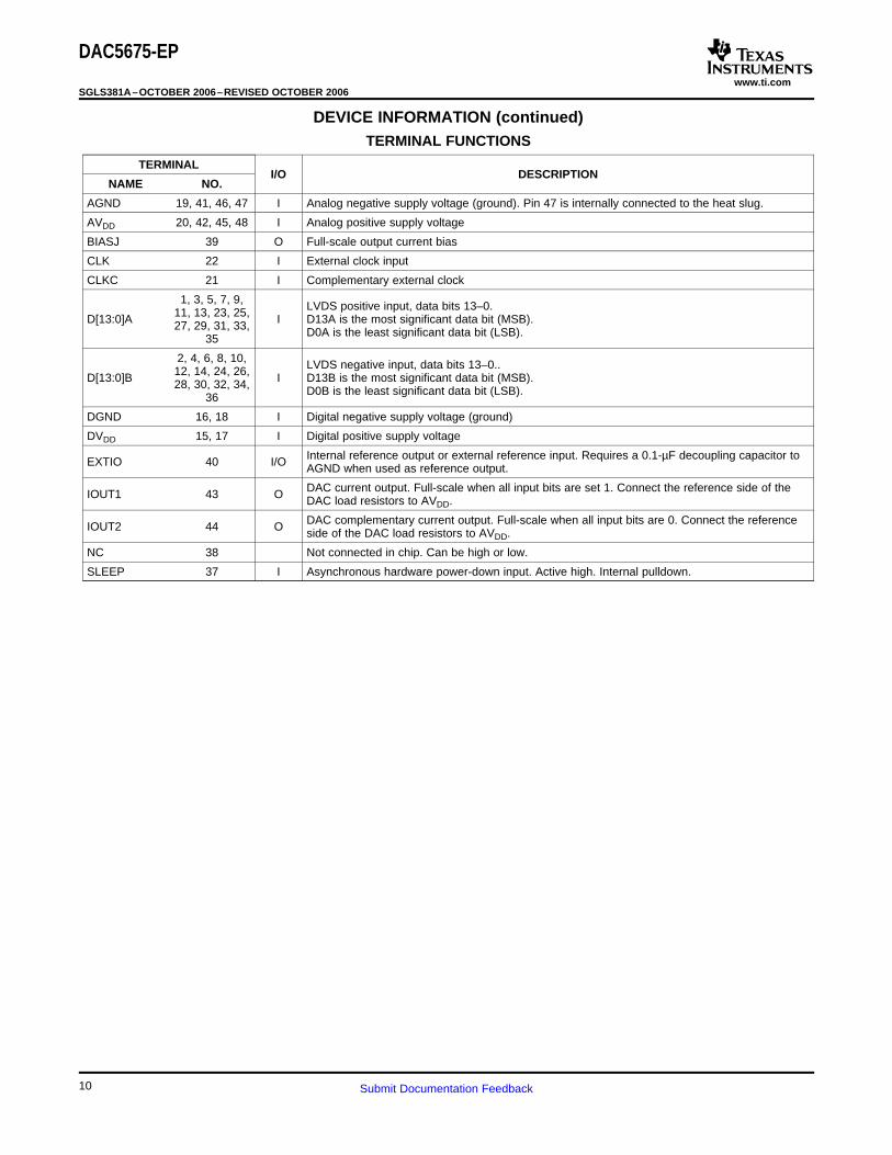
AGND 19, 41, 46, 47 I Analog negative supply voltage (ground). Pin 47 is internally connected to the heat slug.
AVDD 20, 42, 45, 48 I Analog positive supply voltage
BIASJ 39 O Full-scale output current bias
CLK 22 I External clock input
CLKC 21 I Complementary external clock
1, 3, 5, 7, 9, LVDS positive input, data bits 13–0.11, 13, 23, 25,D[13:0]A I D13A is the most significant data bit (MSB).27, 29, 31, 33, D0A is the least significant data bit (LSB).35
2, 4, 6, 8, 10, LVDS negative input, data bits 13–0..12, 14, 24, 26,D[13:0]B I D13B is the most significant data bit (MSB).28, 30, 32, 34, D0B is the least significant data bit (LSB).36
DGND 16, 18 I Digital negative supply voltage (ground)
DVDD 15, 17 I Digital positive supply voltage
Internal reference output or external reference input. Requires a 0.1-µF decoupling capacitor toEXTIO 40 I/O AGND when used as reference output.
DAC current output. Full-scale when all input bits are set 1. Connect the reference side of theIOUT1 43 O DAC load resistors to AVDD.
DAC complementary current output. Full-scale when all input bits are 0. Connect the referenceIOUT2 44 O side of the DAC load resistors to AVDD.
NC 38 Not connected in chip. Can be high or low.
SLEEP 37 I Asynchronous hardware power-down input. Active high. Internal pulldown.
10 Submit Documentation Feedback
www.ti.com
TYPICAL CHARACTERISTICS
Input Code
DN
L (
LS
B)
0 2000
1.0
0.8
0.6
0.4
0.2
0
−0.2
−0.4
−0.6
−0.8
−1.04000 6000 8000 10000 12000 14000 16000
Input Code
INL
(LS
B)
0 2000
1.5
1.0
0.5
0
−0.5
−1.0
−1.54000 6000 8000 10000 12000 14000 16000
Frequency (MHz)
Pow
er
(dB
FS
)
65
0
−10
−20
−30
−40
−50
−60
−70
−80
−90
−10067 69 71 73 75
f1 = 69.5 MHz, −6 dBFS
f2 = 70.5 MHz, −6 dBFS
IMD3 = 77.41 dBc
VCC = VAA= 3.3 V
fCLK = 200 MHz
Center Frequency (MHz)
Tw
o-T
on
e IM
D3 (
dB
c)
90
8886
84
8280
78
76
7472
70
68
6664
62
605 15 25 35 45 55 65 75 85
f2 − f1 = 1 MHz ( 6 dBFS each)–
VCC = VAA = 3.3 V
fCLK = 200 MHz
Frequency (MHz)
Pow
er
(dB
FS
)
0 4020
0
−10
−20
−30
−40
−50
−60
−70
−80
−9080 10060 120 140 160 180 200
VCC = VAA = 3.3 V
fCLK = 400 MHz
fOUT = 20.1 MHz, 0 dBFS
SFDR = 74.75 dBc
20.1 MHz
40.06 MHz
60.25 MHz
Output Frequency (MHz)
SF
DR
(dB
FS
)
90
86
82
78
74
70
66
62
58
54
5010 3020 50 6040 8070 90 100 110 120
VCC = VAA = 3.3 V
fCLK = 400 MHz
0 dBFS
−3 dBFS
−6 dBFS
DAC5675-EP
SGLS381A–OCTOBER 2006–REVISED OCTOBER 2006
DIFFERENTIAL NONLINEARITY (DNL) vs INPUT CODE INTEGRAL NONLINEARITY (INL) vs INPUT CODE
Figure 3. Figure 4.
TWO-TONE IMD (POWER) vs FREQUENCY TWO-TONE IMD3 vs FREQUENCY
Figure 5. Figure 6.
SINGLE-TONE SPECTRUMPOWER vs FREQUENCY SPURIOUS-FREE DYNAMIC RANGE vs FREQUENCY
Figure 7. Figure 8.
11Submit Documentation Feedback

www.ti.com
Output Frequency (MHz)
SF
DR
(dB
FS
)
90
86
82
78
74
70
66
62
58
54
5010 3020 50 6040 8070 90 100 110 120
VCC = VAA = 3.3 V
fCLK = 200 MHz
0 dBFS
−3 dBFS
−6 dBFS
Frequency
Pow
er
(dB
m/3
0kH
z)
18
−25
−35
−45
−55
−65
−75
−85
−95
−105
−11523 28 33 38 43
VCC = VAA = 3.3 V
fCLK = 122.88 MHz
fCENTER = 30.72 MHz
ACLR = 72.29 dB
Frequency
Po
wer
(dB
m/3
0kH
z)
82.2
−30
−40
−50
−60
−70
−80
−90
−100
−11087.2 92.2 97.2 10.2
VCC = VAA = 3.3 V fCLK = 368.64 MHz
fCENTER =
92.16 MHz
ACLR = 65 dBc
Output Frequency (MHz)
AC
LR
(dB
c)80
78
76
74
72
70
68
66
64
62
6010 30 50 70 90 110 130 150
VCC = VAA = 3.3 V
fCLK = 399.36 MHz
Single Channel
DAC5675-EP
SGLS381A–OCTOBER 2006–REVISED OCTOBER 2006
TYPICAL CHARACTERISTICS (continued)
W-CDMA TM1 SINGLE CARRIERSPURIOUS-FREE DYNAMIC RANGE vs FREQUENCY POWER vs FREQUENCY
Figure 9. Figure 10.
W-CDMA TM1 DUAL CARRIER W-CDMA TM1 SINGLE CARRIERPOWER vs FREQUENCY ACLR vs OUTPUT FREQUENCY
Figure 11. Figure 12.
12 Submit Documentation Feedback
www.ti.com
APPLICATION INFORMATION
Detailed Description
Bandgap
Reference
1.2 V
Control Amp
Current
Source
Array
Output
Current
Switches
DAC
Latch
+
Drivers
DecoderInput
Latches
LVDS
Input
Interface
Clock Distribution
SLEEP
EXTIO
BIASJ
D[13:0]A
D[13:0]B
CLK
CLKC
DVDD(2x) DGND(2x)
14
14
AVDD(4x) AGND(4x)
CEXT
0.1 Fm
RBIAS
1 kΩ
1:4
Clock
Input
RT
200 Ω
3.3 V
(AVDD)
3.3 V
(AVDD)
3.3 V
(AVDD)
100 Ω
50 Ω
50 Ω
IOUT
IOUT
1:1Output
RLOAD
50 Ω
DAC5675-EP
DAC5675-EP
SGLS381A–OCTOBER 2006–REVISED OCTOBER 2006
Figure 13 shows a simplified block diagram of the current steering DAC5675. The DAC5675 consists of asegmented array of NPN-transistor current sources, capable of delivering a full-scale output current up to20 mA. Differential current switches direct the current of each current source to either one of the complementaryoutput nodes IOUT1 or IOUT2. The complementary current output enables differential operation, canceling outcommon-mode noise sources (digital feedthrough, on-chip, and PCB noise), dc offsets, and even-orderdistortion components, and doubling signal output power.
The full-scale output current is set using an external resistor (RBIAS) in combination with an on-chip bandgapvoltage reference source (1.2 V) and control amplifier. The current (IBIAS) through resistor RBIAS is mirroredinternally to provide a full-scale output current equal to 16 times IBIAS. The full-scale current is adjustable from20 mA down to 2 mA by using the appropriate bias resistor value.
Figure 13. Application Schematic
13Submit Documentation Feedback
www.ti.com
Digital Inputs
Internal
Digital In
110-Ω
Termination
Resistor
Internal
Digital In
D[13:0]A
D[13..0]A
D[13..0]B
D[13:0]B
DGND
DVDD
DAC5675-EPDAC5675-EP
Internal
Digital In
DVDD
DGND
Digital Input
DAC5675-EP
Clock Input
DAC5675-EP
SGLS381A–OCTOBER 2006–REVISED OCTOBER 2006
APPLICATION INFORMATION (continued)
The DAC5675 uses a low-voltage differential signaling (LVDS) bus input interface. The LVDS features a lowdifferential voltage swing with low constant power consumption (4 mA per complementary data input) acrossfrequency. The differential characteristic of LVDS allows for high-speed data transmission with lowelectromagnetic interference (EMI) levels. The LVDS input minimum and maximum input threshold table lists theLVDS input levels. Figure 14 shows the equivalent complementary digital input interface for the DAC5675, validfor pins D[13:0]A and D[13:0]B. Note that the LVDS interface features internal 110-Ω resistors for propertermination. Figure 2 shows the LVDS input timing measurement circuit and waveforms. A common-mode levelof 1.2 V and a differential input swing of 0.8 VPP is applied to the inputs.
Figure 15 shows a schematic of the equivalent CMOS/TTL-compatible digital inputs of the DAC5675, valid forthe SLEEP pin.
Figure 14. LVDS Digital Equivalent Input
Figure 15. CMOS/TTL Digital Equivalent Input
The DAC5675 features differential LVPECL-compatible clock inputs (CLK, CLKC). Figure 16 shows theequivalent schematic of the clock input buffer. The internal biasing resistors set the input common-mode voltageto approximately 2 V, while the input resistance is typically 670 Ω. A variety of clock sources can be ac-coupledto the device, including a sine-wave source (see Figure 17).
14 Submit Documentation Feedback

www.ti.com
Internal
Clock
CLKC
AGND
AVDD
CLK
R1
1 kΩ
R1
1 kΩ
R2
2 kΩ
R2
2 kΩ
DAC5675-EP
CLK
CLKC
Optional, may be
bypassed for sine-
wave input
RT
200 Ω
Swing Limitation
Termination
Resistor
1:4
CAC
0.1 mF
DAC5675-EP
CLK
CLKC
Single-Ended
ECL
or
(LV)PECL
Source
ECL/PECL
Gate
CAC
RT
50 Ω
RT
50 Ω
VTT
CAC
0.01 mF
0.01 mFDAC5675-EP
DAC5675-EP
SGLS381A–OCTOBER 2006–REVISED OCTOBER 2006
APPLICATION INFORMATION (continued)
Figure 16. Clock Equivalent Input
Figure 17. Driving the DAC5675 With a Single-Ended Clock Source Using a Transformer
To obtain best ac performance, the DAC5675 clock input should be driven with a differential LVPECL orsine-wave source as shown in Figure 18 and Figure 19. Here, the potential of VTT should be set to thetermination voltage required by the driver along with the proper termination resistors (RT). The DAC5675 clockinput can also be driven single ended; this is shown in Figure 20.
Figure 18. Driving the DAC5675 With a Single-Ended ECL/PECL Clock Source
15Submit Documentation Feedback
www.ti.com
CLK
CLKC
CAC
RT
50 Ω
RT
50 Ω
VTT
CAC
0.01 mF
0.01 mF
DifferentialECLor
(LV)PECLSource
+
−
DAC5675-EP
CLK
CLKC
0.01mF
ROPT
22 Ω
TTL/CMOS
Source
Node CLKC
Internally Biased to
AVDD/2
DAC5675-EP
Supply Inputs
DAC Transfer Function
IOUT1 IO(FS)IOUT2 (1)
IOUT1 IO(FS) CODE
16384 (2)
IOUT2
IO(FS) (16383CODE)16384 (3)
DAC5675-EP
SGLS381A–OCTOBER 2006–REVISED OCTOBER 2006
APPLICATION INFORMATION (continued)
Figure 19. Driving the DAC5675 With a Differential ECL/PECL Clock Source
Figure 20. Driving the DAC5675 With a Single-Ended TTL/CMOS Clock Source
The DAC5675 comprises separate analog and digital supplies, that is AVDD and DVDD, respectively. Thesesupply inputs can be set independently from 3.6 V down to 3.15 V.
The DAC5675 delivers complementary output currents IOUT1 and IOUT2. The DAC supports straight binarycoding, with D13 being the MSB and D0 the LSB. (For ease of notation, we denote D13–D0 as the logical bitequivalent of the complementary LVDS inputs D[13:0]A and D[13:0]B). Output current IOUT1 equals theapproximate full-scale output current when all input bits are set high, when the binary input word has the decimalrepresentation 16383. Full-scale output current flows through terminal IOUT2 when all input bits are set low(mode 0, straight binary input). The relation between IOUT1 and IOUT2 can thus be expressed as:
where IO(FS) is the full-scale output current. The output currents can be expressed as:
where CODE is the decimal representation of the DAC data input word. Output currents IOUT1 and IOUT2 drivea load RL. RL is the combined impedance for the termination resistance and/or transformer load resistance,RLOAD (see Figure 22 and Figure 23). This would translate into single-ended voltages VOUT1 and VOUT2 atterminal IOUT1 and IOUT2, respectively, of Equation 4 and Equation 5:
16 Submit Documentation Feedback
www.ti.com
VOUT1 IOUT1 RL CODE IO(FS) RL
16384 (4)
VOUT2 IOUT2 RL (16383CODE) IO(FS) RL
16384 (5)
VOUT (DIFF) VOUT1VOUT2
(2CODE 16383) IO(FS) RL
16384 (6)
Reference Operation
IO(FS) 16 IBIAS16 VEXTIO
RBIAS (7)
Analog Current Outputs
DAC5675-EP
SGLS381A–OCTOBER 2006–REVISED OCTOBER 2006
APPLICATION INFORMATION (continued)
Thus, the differential output voltage VOUT(DIFF) can be expressed as:
Equation 6 shows that applying the differential output results in doubling the signal power delivered to the load.Since the output currents IOUT1 and IOUT2 are complementary, they become additive when processeddifferentially. Care should be taken not to exceed the compliance voltages at nodes IOUT1 and IOUT2, whichleads to increased signal distortion.
The DAC5675 has a bandgap reference and control amplifier for biasing the full-scale output current. Thefull-scale output current is set by applying an external resistor RBIAS. The bias current IBIAS through resistor RBIASis defined by the on-chip bandgap reference voltage and control amplifier. The full-scale output current equals16 times this bias current. The full-scale output current IO(FS) is thus expressed as Equation 7:
where VEXTIO is the voltage at terminal EXTIO. The bandgap reference voltage delivers a stable voltage of 1.2 V.This reference can be overridden by applying an external voltage to terminal EXTIO. The bandgap referencecan additionally be used for external reference operation. In such a case, an external buffer amplifier with highimpedance input should be selected in order to limit the bandgap load current to less than 100 nA. The capacitorCEXT may be omitted. Terminal EXTIO serves as either an input or output node. The full-scale output current isadjustable from 20 mA down to 2 mA by varying resistor RBIAS.
Figure 21 shows a simplified schematic of the current source array output with corresponding switches.Differential NPN switches direct the current of each individual NPN current source to either the positive outputnode IOUT1 or its complementary negative output node IOUT2. The output impedance is determined by thestack of the current sources and differential switches and is >300 kΩ in parallel with an output capacitanceof 5 pF.
The external output resistors are referred to the positive supply AVDD.
17Submit Documentation Feedback

www.ti.com
S(1) S(1)C S(2)C S(N)CS(2) S(N)
Current Sink Array
IOUT1 IOUT2
RLOADRLOAD
3.3 V
AVDD
AGND
DAC5675-EP
IOUT1
IOUT2
3.3 V
AVDD
3.3 V
AVDD
50 Ω
50 Ω
100 Ω
1:1
RLOAD
50 ΩDAC5675-EP
DAC5675-EP
SGLS381A–OCTOBER 2006–REVISED OCTOBER 2006
APPLICATION INFORMATION (continued)
Figure 21. Equivalent Analog Current Output
The DAC5675 can easily be configured to drive a doubly-terminated 50-Ω cable using a properly selectedtransformer. Figure 22 and Figure 23 show the 1:1 and 4:1 impedance ratio configuration, respectively. Theseconfigurations provide maximum rejection of common-mode noise sources and even-order distortioncomponents, thereby doubling the power of the DAC to the output. The center tap on the primary side of thetransformer is terminated to AVDD, enabling a dc-current flow for both IOUT1 and IOUT2. Note that the acperformance of the DAC5675 is optimum and specified using a 1:1 differential transformer-coupled output.
Figure 22. Driving a Doubly-Terminated 50-Ω Cable Using a 1:1 Impedance Ratio Transformer
18 Submit Documentation Feedback

www.ti.com
IOUT1
IOUT2
3.3 V
AVDD
3.3 V
AVDD
100 Ω
100 Ω
4:1
RLOAD
50 Ω
15 Ω
DAC5675-EP
(a)
VOUT
3.3 V
AVDD
3.3 V
AVDD
25 Ω
25 Ω
VOUT1
VOUT2
Optional, for single-
ended output
referred to AVDD
IOUT1
IOUT2
CFB
IOUT1
IOUT2
3.3 V
AVDD
200 Ω (RFB)
(b)
DAC5675-EPDAC5675-EP
Sleep Mode
DAC5675-EP
SGLS381A–OCTOBER 2006–REVISED OCTOBER 2006
APPLICATION INFORMATION (continued)
Figure 23. Driving a Doubly-Terminated 50-Ω Cable Using a 4:1 Impedance Ratio Transformer
Figure 24(a) shows the typical differential output configuration with two external matched resistor loads. Thenominal resistor load of 25 Ω gives a differential output swing of 1 VPP (0.5 VPP single ended) when applying a20-mA full-scale output current. The output impedance of the DAC5675 slightly depends on the output voltage atnodes IOUT1 and IOUT2. Consequently, for optimum dc-integral nonlinearity, the configuration of Figure 24(b)should be chosen. In this current/voltage (I-V) configuration, terminal IOUT1 is kept at AVDD by the invertingoperational amplifier. The complementary output should be connected to AVDD to provide a dc-current path forthe current sources switched to IOUT1. The amplifier maximum output swing and the full-scale output current ofthe DAC determine the value of the feedback resistor RFB. The capacitor CFB filters the steep edges of theDAC5675 current output, thereby reducing the operational amplifier slew-rate requirements. In this configuration,the operational amplifier should operate at a supply voltage higher than the resistor output reference voltageAVDD as a result of its positive and negative output swing around AVDD. Node IOUT1 should be selected if asingle-ended unipolar output is desired.
Figure 24. Output Configurations
The DAC5675 features a power-down mode that turns off the output current and reduces the supply current toapproximately 6 mA. The power-down mode is activated by applying a logic level one to the SLEEP pin, pulleddown internally.
19Submit Documentation Feedback

www.ti.com
DEFINITIONS
Definitions of Specifications and Terminology
DAC5675-EP
SGLS381A–OCTOBER 2006–REVISED OCTOBER 2006
Gain error is defined as the percentage error in the ratio between the measured full-scale output current andthe value of 16 × V(EXTIO)/RBIAS. A V(EXTIO) of 1.25 V is used to measure the gain error with an external referencevoltage applied. With an internal reference, this error includes the deviation of V(EXTIO) (internal bandgapreference voltage) from the typical value of 1.25 V.
Offset error is defined as the percentage error in the ratio of the differential output current (IOUT1-IOUT2) andthe half of the full-scale output current for input code 8192.
THD is the ratio of the rms sum of the first six harmonic components to the rms value of the fundamental outputsignal.
SNR is the ratio of the rms value of the fundamental output signal to the rms sum of all other spectralcomponents below the Nyquist frequency, including noise, but excluding the first six harmonics and dc.
SINAD is the ratio of the rms value of the fundamental output signal to the rms sum of all other spectralcomponents below the Nyquist frequency, including noise and harmonics, but excluding dc.
ACPR or adjacent channel power ratio is defined for a 3.84-Mcps 3GPP W-CDMA input signal measured in a3.84-MHz bandwidth at a 5-MHz offset from the carrier with a 12-dB peak-to-average ratio.
APSSR or analog power supply ratio is the percentage variation of full-scale output current versus a 5%variation of the analog power supply AVDD from the nominal. This is a dc measurement.
DPSSR or digital power supply ratio is the percentage variation of full-scale output current versus a 5% variationof the digital power supply DVDD from the nominal. This is a dc measurement.
20 Submit Documentation Feedback

PACKAGE OPTION ADDENDUM
www.ti.com 31-May-2014
Addendum-Page 1
PACKAGING INFORMATION
Orderable Device Status(1)
Package Type PackageDrawing
Pins PackageQty
Eco Plan(2)
Lead/Ball Finish(6)
MSL Peak Temp(3)
Op Temp (°C) Device Marking(4/5)
Samples
DAC5675MPHPEP ACTIVE HTQFP PHP 48 250 Green (RoHS& no Sb/Br)
CU NIPDAU Level-3-260C-168 HR -55 to 125 DC5675MEP
DAC5675MPHPREP ACTIVE HTQFP PHP 48 1000 Green (RoHS& no Sb/Br)
CU NIPDAU Level-3-260C-168 HR -55 to 125 DC5675MEP
V62/05619-01XE ACTIVE HTQFP PHP 48 1000 Green (RoHS& no Sb/Br)
CU NIPDAU Level-3-260C-168 HR -55 to 125 DC5675MEP
V62/05619-02XE ACTIVE HTQFP PHP 48 250 Green (RoHS& no Sb/Br)
CU NIPDAU Level-3-260C-168 HR -55 to 125 DC5675MEP
(1) The marketing status values are defined as follows:ACTIVE: Product device recommended for new designs.LIFEBUY: TI has announced that the device will be discontinued, and a lifetime-buy period is in effect.NRND: Not recommended for new designs. Device is in production to support existing customers, but TI does not recommend using this part in a new design.PREVIEW: Device has been announced but is not in production. Samples may or may not be available.OBSOLETE: TI has discontinued the production of the device.
(2) Eco Plan - The planned eco-friendly classification: Pb-Free (RoHS), Pb-Free (RoHS Exempt), or Green (RoHS & no Sb/Br) - please check http://www.ti.com/productcontent for the latest availabilityinformation and additional product content details.TBD: The Pb-Free/Green conversion plan has not been defined.Pb-Free (RoHS): TI's terms "Lead-Free" or "Pb-Free" mean semiconductor products that are compatible with the current RoHS requirements for all 6 substances, including the requirement thatlead not exceed 0.1% by weight in homogeneous materials. Where designed to be soldered at high temperatures, TI Pb-Free products are suitable for use in specified lead-free processes.Pb-Free (RoHS Exempt): This component has a RoHS exemption for either 1) lead-based flip-chip solder bumps used between the die and package, or 2) lead-based die adhesive used betweenthe die and leadframe. The component is otherwise considered Pb-Free (RoHS compatible) as defined above.Green (RoHS & no Sb/Br): TI defines "Green" to mean Pb-Free (RoHS compatible), and free of Bromine (Br) and Antimony (Sb) based flame retardants (Br or Sb do not exceed 0.1% by weightin homogeneous material)
(3) MSL, Peak Temp. - The Moisture Sensitivity Level rating according to the JEDEC industry standard classifications, and peak solder temperature.
(4) There may be additional marking, which relates to the logo, the lot trace code information, or the environmental category on the device.
(5) Multiple Device Markings will be inside parentheses. Only one Device Marking contained in parentheses and separated by a "~" will appear on a device. If a line is indented then it is a continuationof the previous line and the two combined represent the entire Device Marking for that device.
(6) Lead/Ball Finish - Orderable Devices may have multiple material finish options. Finish options are separated by a vertical ruled line. Lead/Ball Finish values may wrap to two lines if the finishvalue exceeds the maximum column width.
PACKAGE OPTION ADDENDUM
www.ti.com 31-May-2014
Addendum-Page 2
Important Information and Disclaimer:The information provided on this page represents TI's knowledge and belief as of the date that it is provided. TI bases its knowledge and belief on informationprovided by third parties, and makes no representation or warranty as to the accuracy of such information. Efforts are underway to better integrate information from third parties. TI has taken andcontinues to take reasonable steps to provide representative and accurate information but may not have conducted destructive testing or chemical analysis on incoming materials and chemicals.TI and TI suppliers consider certain information to be proprietary, and thus CAS numbers and other limited information may not be available for release.
In no event shall TI's liability arising out of such information exceed the total purchase price of the TI part(s) at issue in this document sold by TI to Customer on an annual basis.
OTHER QUALIFIED VERSIONS OF DAC5675-EP :
• Catalog: DAC5675
NOTE: Qualified Version Definitions:
• Catalog - TI's standard catalog product
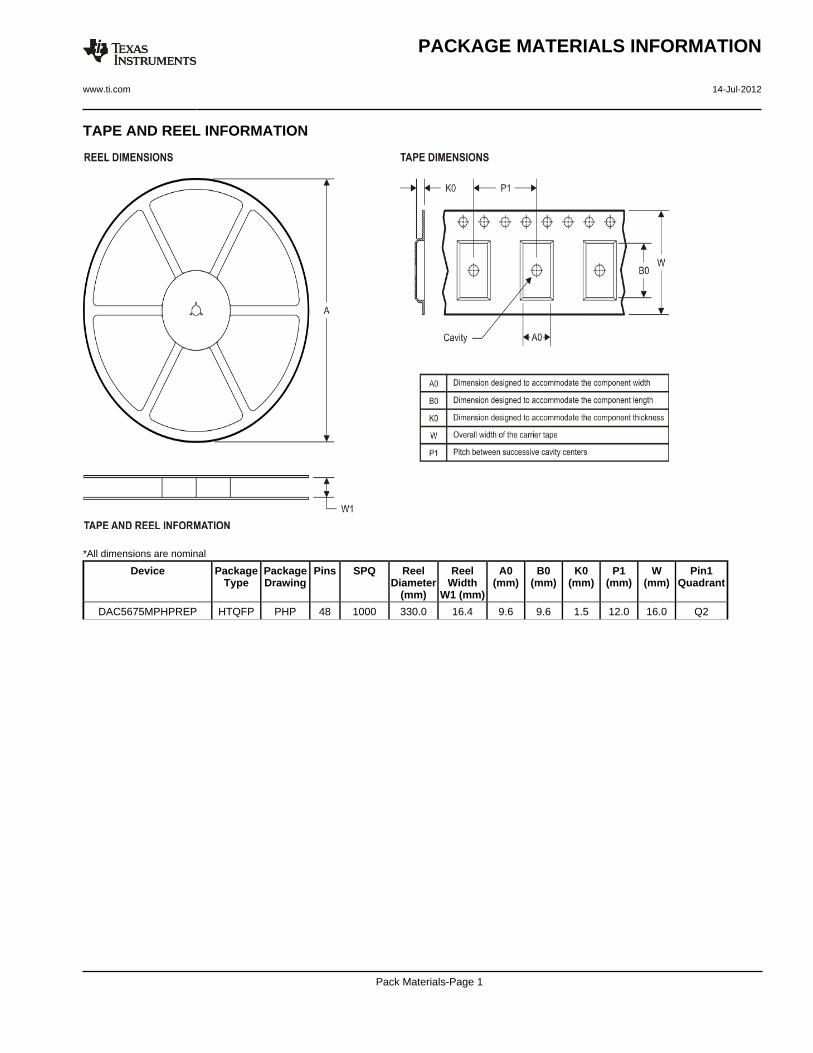
TAPE AND REEL INFORMATION
*All dimensions are nominal
Device PackageType
PackageDrawing
Pins SPQ ReelDiameter
(mm)
ReelWidth
W1 (mm)
A0(mm)
B0(mm)
K0(mm)
P1(mm)
W(mm)
Pin1Quadrant
DAC5675MPHPREP HTQFP PHP 48 1000 330.0 16.4 9.6 9.6 1.5 12.0 16.0 Q2
PACKAGE MATERIALS INFORMATION
www.ti.com 14-Jul-2012
Pack Materials-Page 1

*All dimensions are nominal
Device Package Type Package Drawing Pins SPQ Length (mm) Width (mm) Height (mm)
DAC5675MPHPREP HTQFP PHP 48 1000 367.0 367.0 38.0
PACKAGE MATERIALS INFORMATION
www.ti.com 14-Jul-2012
Pack Materials-Page 2


IMPORTANT NOTICETexas Instruments Incorporated and its subsidiaries (TI) reserve the right to make corrections, enhancements, improvements and otherchanges to its semiconductor products and services per JESD46, latest issue, and to discontinue any product or service per JESD48, latestissue. Buyers should obtain the latest relevant information before placing orders and should verify that such information is current andcomplete. All semiconductor products (also referred to herein as “components”) are sold subject to TI’s terms and conditions of salesupplied at the time of order acknowledgment.TI warrants performance of its components to the specifications applicable at the time of sale, in accordance with the warranty in TI’s termsand conditions of sale of semiconductor products. Testing and other quality control techniques are used to the extent TI deems necessaryto support this warranty. Except where mandated by applicable law, testing of all parameters of each component is not necessarilyperformed.TI assumes no liability for applications assistance or the design of Buyers’ products. Buyers are responsible for their products andapplications using TI components. To minimize the risks associated with Buyers’ products and applications, Buyers should provideadequate design and operating safeguards.TI does not warrant or represent that any license, either express or implied, is granted under any patent right, copyright, mask work right, orother intellectual property right relating to any combination, machine, or process in which TI components or services are used. Informationpublished by TI regarding third-party products or services does not constitute a license to use such products or services or a warranty orendorsement thereof. Use of such information may require a license from a third party under the patents or other intellectual property of thethird party, or a license from TI under the patents or other intellectual property of TI.Reproduction of significant portions of TI information in TI data books or data sheets is permissible only if reproduction is without alterationand is accompanied by all associated warranties, conditions, limitations, and notices. TI is not responsible or liable for such altereddocumentation. Information of third parties may be subject to additional restrictions.Resale of TI components or services with statements different from or beyond the parameters stated by TI for that component or servicevoids all express and any implied warranties for the associated TI component or service and is an unfair and deceptive business practice.TI is not responsible or liable for any such statements.Buyer acknowledges and agrees that it is solely responsible for compliance with all legal, regulatory and safety-related requirementsconcerning its products, and any use of TI components in its applications, notwithstanding any applications-related information or supportthat may be provided by TI. Buyer represents and agrees that it has all the necessary expertise to create and implement safeguards whichanticipate dangerous consequences of failures, monitor failures and their consequences, lessen the likelihood of failures that might causeharm and take appropriate remedial actions. Buyer will fully indemnify TI and its representatives against any damages arising out of the useof any TI components in safety-critical applications.In some cases, TI components may be promoted specifically to facilitate safety-related applications. With such components, TI’s goal is tohelp enable customers to design and create their own end-product solutions that meet applicable functional safety standards andrequirements. Nonetheless, such components are subject to these terms.No TI components are authorized for use in FDA Class III (or similar life-critical medical equipment) unless authorized officers of the partieshave executed a special agreement specifically governing such use.Only those TI components which TI has specifically designated as military grade or “enhanced plastic” are designed and intended for use inmilitary/aerospace applications or environments. Buyer acknowledges and agrees that any military or aerospace use of TI componentswhich have not been so designated is solely at the Buyer's risk, and that Buyer is solely responsible for compliance with all legal andregulatory requirements in connection with such use.TI has specifically designated certain components as meeting ISO/TS16949 requirements, mainly for automotive use. In any case of use ofnon-designated products, TI will not be responsible for any failure to meet ISO/TS16949.Products ApplicationsAudio www.ti.com/audio Automotive and Transportation www.ti.com/automotiveAmplifiers amplifier.ti.com Communications and Telecom www.ti.com/communicationsData Converters dataconverter.ti.com Computers and Peripherals www.ti.com/computersDLP® Products www.dlp.com Consumer Electronics www.ti.com/consumer-appsDSP dsp.ti.com Energy and Lighting www.ti.com/energyClocks and Timers www.ti.com/clocks Industrial www.ti.com/industrialInterface interface.ti.com Medical www.ti.com/medicalLogic logic.ti.com Security www.ti.com/securityPower Mgmt power.ti.com Space, Avionics and Defense www.ti.com/space-avionics-defenseMicrocontrollers microcontroller.ti.com Video and Imaging www.ti.com/videoRFID www.ti-rfid.comOMAP Applications Processors www.ti.com/omap TI E2E Community e2e.ti.comWireless Connectivity www.ti.com/wirelessconnectivity
Mailing Address: Texas Instruments, Post Office Box 655303, Dallas, Texas 75265Copyright © 2014, Texas Instruments Incorporated