
DAC38RF8x-EVM User's Guide - Mouser Electronics · DAC38RF8x-EVM User's Guide SLAU671–October...
21
1 SLAU671 – October 2016 Submit Documentation Feedback Copyright © 2016, Texas Instruments Incorporated DAC38RF8x-EVM User's Guide SLAU671 – October 2016 DAC38RF8x-EVM The DAC38RF8x-EVM is the circuit board for evaluating the DAC38RF83 and DAC38RF80 (DAC38RF8x) digital-to-analog converters (DACs). This document is intended to guide the DAC38RF8x-EVM user through the process of setting up the EVM successfully. For other information on the DAC38RF8x, refer to the device datasheet (SLASEA3). Throughout this document, italics are used to refer to names of controls on graphical user interfaces (GUI). Contents 1 Introduction ................................................................................................................... 2 1.1 Required Hardware and Software ................................................................................ 2 1.2 HSDC Pro Software Patch Installation Guidelines ............................................................. 2 1.3 HSDC Pro Software Patch Installation Guidelines ............................................................. 2 2 EVM Block Diagram ......................................................................................................... 3 3 Quick Start .................................................................................................................... 4 3.1 TSW14J56 and DAC38RF8x-EVM ............................................................................... 4 4 Known Issues ............................................................................................................... 13 Appendix A ....................................................................................................................... 14 Appendix B ....................................................................................................................... 15 List of Figures 1 HSDC Pro Patch v4.0.01 ................................................................................................... 2 2 DAC38RF8x-EVM Block Diagram ......................................................................................... 3 3 Shunt Pin 1 and Pin 2 of JP10 Jumper Enabling External Clock Mode .............................................. 4 4 DAC38RF83 EVM Setup for External Clock Mode...................................................................... 5 5 DAC38RF8x-EVM GUI Quick Start Page Configured for External Clock Mode..................................... 6 6 Open Pin 1 and Pin 2 of JP10 Jumper to Enable On-Chip PLL Clock Mode........................................ 7 7 DAC38RF83 EVM Setup for On-Chip PLL Mode ....................................................................... 7 8 DAC38RF8x-EVM GUI Quick Start Page Configured for On-Chip PLL Mode ...................................... 8 9 Load Firmware to the TSW14J56 ......................................................................................... 9 10 Complex, Single Tone Generation at 100 kHz in HSDC Pro......................................................... 10 11 DAC A Digital Control Tab of the DAC38RF8x GUI ................................................................... 10 12 DAC A Output at 1960 MHz and 2140 MHz, Mixer Gain Off, Dummy Date Enabled............................. 11 13 1×20 MHz LTE, TM3.1, Center Frequency = 1960 MHz, DAC Coarse Gain = 10, External Clock ............. 12 14 1×20 MHz LTE, TM3.1, Center Frequency = 2140 MHz, DAC Coarse Gain = 10, External Clock ............. 12 15 DAC Output Power vs Frequency (Fsampling = 8847.36 Msps) .................................................... 13 16 DAC Output Circuit Schematic ........................................................................................... 14 17 TCM3-452X-1+ Frequency Response................................................................................... 14 18 Clock Input Path Circuit Diagram ........................................................................................ 15 19 NCR2-113+ Frequency Response ....................................................................................... 15
Transcript of DAC38RF8x-EVM User's Guide - Mouser Electronics · DAC38RF8x-EVM User's Guide SLAU671–October...
1SLAU671–October 2016Submit Documentation Feedback
Copyright © 2016, Texas Instruments Incorporated
DAC38RF8x-EVM
User's GuideSLAU671–October 2016
DAC38RF8x-EVM
The DAC38RF8x-EVM is the circuit board for evaluating the DAC38RF83 and DAC38RF80 (DAC38RF8x)digital-to-analog converters (DACs). This document is intended to guide the DAC38RF8x-EVM userthrough the process of setting up the EVM successfully. For other information on the DAC38RF8x, refer tothe device datasheet (SLASEA3). Throughout this document, italics are used to refer to names of controlson graphical user interfaces (GUI).
Contents1 Introduction ................................................................................................................... 2
1.1 Required Hardware and Software ................................................................................ 21.2 HSDC Pro Software Patch Installation Guidelines ............................................................. 21.3 HSDC Pro Software Patch Installation Guidelines ............................................................. 2
2 EVM Block Diagram ......................................................................................................... 33 Quick Start .................................................................................................................... 4
3.1 TSW14J56 and DAC38RF8x-EVM ............................................................................... 44 Known Issues ............................................................................................................... 13Appendix A ....................................................................................................................... 14Appendix B ....................................................................................................................... 15
List of Figures
1 HSDC Pro Patch v4.0.01 ................................................................................................... 22 DAC38RF8x-EVM Block Diagram ......................................................................................... 33 Shunt Pin 1 and Pin 2 of JP10 Jumper Enabling External Clock Mode .............................................. 44 DAC38RF83 EVM Setup for External Clock Mode...................................................................... 55 DAC38RF8x-EVM GUI Quick Start Page Configured for External Clock Mode..................................... 66 Open Pin 1 and Pin 2 of JP10 Jumper to Enable On-Chip PLL Clock Mode........................................ 77 DAC38RF83 EVM Setup for On-Chip PLL Mode ....................................................................... 78 DAC38RF8x-EVM GUI Quick Start Page Configured for On-Chip PLL Mode ...................................... 89 Load Firmware to the TSW14J56 ......................................................................................... 910 Complex, Single Tone Generation at 100 kHz in HSDC Pro......................................................... 1011 DAC A Digital Control Tab of the DAC38RF8x GUI ................................................................... 1012 DAC A Output at 1960 MHz and 2140 MHz, Mixer Gain Off, Dummy Date Enabled............................. 1113 1×20 MHz LTE, TM3.1, Center Frequency = 1960 MHz, DAC Coarse Gain = 10, External Clock ............. 1214 1×20 MHz LTE, TM3.1, Center Frequency = 2140 MHz, DAC Coarse Gain = 10, External Clock ............. 1215 DAC Output Power vs Frequency (Fsampling = 8847.36 Msps) .................................................... 1316 DAC Output Circuit Schematic ........................................................................................... 1417 TCM3-452X-1+ Frequency Response................................................................................... 1418 Clock Input Path Circuit Diagram ........................................................................................ 1519 NCR2-113+ Frequency Response ....................................................................................... 15
Introduction www.ti.com
2 SLAU671–October 2016Submit Documentation Feedback
Copyright © 2016, Texas Instruments Incorporated
DAC38RF8x-EVM
1 Introduction
1.1 Required Hardware and SoftwareThe following hardware and software are required to evaluate the DAC38RF8x device:1. DAC38RF8x-EVM: Main circuit board containing the DAC to be evaluated2. DAC38RF8x-EVM Graphical User Interface (GUI): Software that controls the DAC EVM3. TSW14J56 EVM: Hardware that generates digital patterns for the DAC
http://www.ti.com/tool/TSW14J56EVM4. HSDC Pro software: Software interface that controls the TSW14J56 EVM
http://www.ti.com/tool/dataconverterpro-sw5. Patch for HSDCPROv4.01: Required to enable DAC38RF8x support
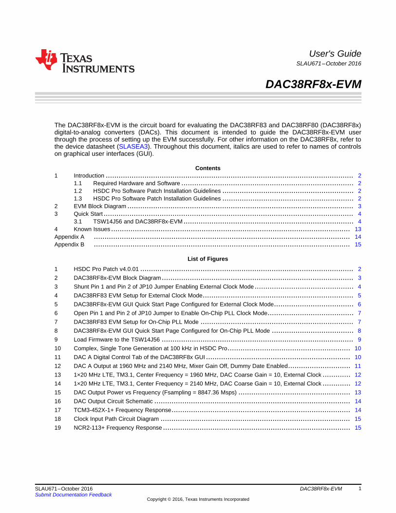
1.2 HSDC Pro Software Patch Installation GuidelinesBy default, the HSDC Pro software (v4.0) does not support the DAC38RF8x-EVM. To enable support forthe DAC38RF8x-EVM:1. Make sure that HSDC Pro GUI is closed.2. Run the executable HSDCPro_Patch.exe. This executable patches the original installation of HSDC
Pro with the necessary files to enable support for DAC38RF8x-EVM.
1.3 HSDC Pro Software Patch Installation Guidelines
NOTE: Only apply the patch to the 4.0 version of HSDC Pro.
Figure 1. HSDC Pro Patch v4.0.01
1:2 Power
Splitter
DA38RF8x
LMK04828
Clock
Divider
(/4)
IOUTA+
IOUTA>
IOUTB>
IOUTB+
SysrefReference
Clock
SMA
SMA J1
SMA
SMA
NCR2-113+
2:1
TCM3-452X-1+
2:1
NB7V33M
FMC Connector
Sysref
Reference
Clock
1.8 V
1.8 V
+ CLKTX>�
SMA
+ CLKIN >
TCM2-43X+
2:1
www.ti.com EVM Block Diagram
3SLAU671–October 2016Submit Documentation Feedback
Copyright © 2016, Texas Instruments Incorporated
DAC38RF8x-EVM
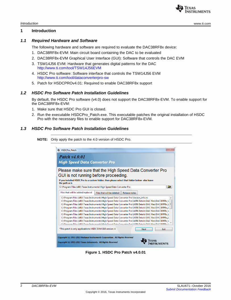
2 EVM Block DiagramFigure 2 illustrates the EVM block diagram.
Figure 2. DAC38RF8x-EVM Block Diagram
Table 1. DAC38RF8xEVM Component Description
Part DescriptionDAC38RF8x 9 Gsps dual-channel DAC with JESD204B interfaceFMC Connector Interface to connect DAC evaluation board to pattern generators (for example, TSW14J56)LMK04828 JESD204B-compliant clock generator. Used to generate sysref and device clock to pattern generator. Also
generates sysref and PLL reference clock to DAC38RF8x.NB7V33M 10 GHz divide by 4 clock dividerTCM3-452X-1+ 2:1 impedance ratio transformer. Used for (1) impedance matching to 50-Ω load, (2) differential to single-ended
conversion, (3) DC biasing of DAC output.TCM2-43X+ 2:1 impedance ratio transformer. Used to convert CLKTX from differential to single ended. CLKTX is divided by
3 or 4 output of the DAC sampling clock.NCR2-113+ 2:1 impedance ratio transformer. Used to convert single-ended input clock to differential for the DAC.
Quick Start www.ti.com
4 SLAU671–October 2016Submit Documentation Feedback
Copyright © 2016, Texas Instruments Incorporated
DAC38RF8x-EVM
3 Quick StartThe following examples use an external clock and the on-chip PLL to evaluate the performance of theDAC38RF8x-EVM. The frequency of the clock is arbitrarily selected as 6144 Msps but the procedureoutlined is applicable to any external clock frequency and any supported on-chip PLL frequency.
The external clock path includes a balun for single-ended to differential conversion. Appendix B shows theinsertion loss, amplitude, and phase un-balance of this balun.
3.1 TSW14J56 and DAC38RF8x-EVMThis section covers details on the TSW14J56 and DAC38RF8x-EVM.1. Make sure both boards are not powered and not connected to the PC’s USB port.2. Connect the FMC connector of TSW14J56 EVM (J4) to FMC connector of DAC38RF8x-EVM (J20).
3.1.1 TSW14J56
1. Connect a 5-V power supply to connector J11 (+5 V IN)2. Connect a USB cable to the USB connector (J9)3. Flip the power switch (SW6) to the “ON” position.
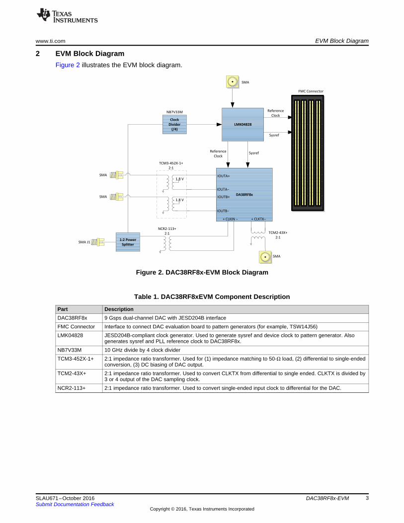
3.1.2 DAC38RF8x-EVM Configuration With External ClockSkip this section if the on-chip PLL is used as the DAC clock source.
NOTE: Shunt pin 1 and pin 2 of the 2-pin jumper labeled JP10 to enable external clock mode. Thisis shown in Figure 3.
Figure 3. Shunt Pin 1 and Pin 2 of JP10 Jumper Enabling External Clock Mode
www.ti.com Quick Start
5SLAU671–October 2016Submit Documentation Feedback
Copyright © 2016, Texas Instruments Incorporated
DAC38RF8x-EVM
Figure 4. DAC38RF83 EVM Setup for External Clock Mode
1. Connect a 5-V power supply to connector J21 (+5V_IN).2. Connect a USB cable to the USB connector (J16).3. Provide a 16-dBm, 6144-MHz, external DAC sampling clock to the clock balun input at J1.
NOTE: There is an on board 1:2 power splitter to route the external clock to the DAC and toTSW14J56EVM through the LMK04828 and a clock divider circuit. Use 18-dBm clock inputpower for > 8 Gsps DAC sample rate.
4. Connect a spectrum analyzer to the DAC output SMA connector:• For DAC38RF83: Connect spectrum analyzer to J6 (DAC A output) or J2 (DAC B output)• For DAC38RF80: Connect a spectrum analyzer to J7 (DAC A output) or J2 (DAC B output)
Quick Start www.ti.com
6 SLAU671–October 2016Submit Documentation Feedback
Copyright © 2016, Texas Instruments Incorporated
DAC38RF8x-EVM
3.1.3 DAC38RF8x Graphical User Interface (GUI)
Figure 5. DAC38RF8x-EVM GUI Quick Start Page Configured for External Clock Mode
1. Start the DAC38RF8x-EVM GUI, then navigate to the quick start page as shown in Figure 52. Verify that the green USB Status indicator on the top right corner is lit. If it is not lit, click the
Reconnect FTDI? button and check the USB Status indicator again.3. On the Quick Start tab, toggle the DAC RESETB Pin button and then click on the Load Default
button. The software automatically configures the DAC to its default state.4. Enter the desired DAC clock frequency (6144 MHz in this example) and specify the desired number of
DACs (Dual DAC), number of IQ pairs(1 IQ pair), number of lanes (4 lanes), and interpolation (16x) asshown in Figure 5
5. Note the messages displayed for information about the serdes rate, maximum allowed sample rate forthe selected mode, and the HSDC Pro ini file to select (see the section on HSDC Pro for moreinformation). If the DAC clock frequency entered is not supported for the selected mode, the DAC clockfrequency box blinks.
6. Click on the CONFIGURE DAC button to load the DAC configuration data.7. Click on the Reset DAC JESD Core button and the Trigger LMK04828 SYSREF button.
www.ti.com Quick Start
7SLAU671–October 2016Submit Documentation Feedback
Copyright © 2016, Texas Instruments Incorporated
DAC38RF8x-EVM
3.1.4 DAC38RF8x-EVM Configuration With On-Chip PLLSkip this section if using an external clock as the DAC clock source.
NOTE: The 2-pin jumper labeled JP10 must be open to enable on-chip PLL clock mode. This isshown in Figure 6.
Figure 6. Open Pin 1 and Pin 2 of JP10 Jumper to Enable On-Chip PLL Clock Mode
Figure 7. DAC38RF83 EVM Setup for On-Chip PLL Mode
Quick Start www.ti.com
8 SLAU671–October 2016Submit Documentation Feedback
Copyright © 2016, Texas Instruments Incorporated
DAC38RF8x-EVM
1. Connect a 5-V power supply to connector J21 (+5 V IN).2. Connect a USB cable to the USB connector (J16).3. Provide a 4–8 dBm external reference clock to SMA J4 as shown in Figure 7. The frequency of this
reference clock is set in a later step.4. Connect a spectrum analyzer to the DAC output SMA connector.
3.1.5 DAC38RF8x Graphical User Interface (GUI)
Figure 8. DAC38RF8x-EVM GUI Quick Start Page Configured for On-Chip PLL Mode
1. Start the DAC38RF8x-EVM GUI then navigate to the quick start page as shown in Figure 8.2. Verify that the green USB Status indicator on the top right corner is lit. If it is not lit, click the
Reconnect FTDI? button and check the USB Status indicator again.3. On the Quick Start tab, toggle the DAC RESETB Pin button and then click the Load Default button.
The software automatically configures the DAC to its default state.4. Check the PLL Enable box and enter the desired on-chip PLL reference clock frequency.
NOTE: The DAC Clock Frequency box automatically updates based on the M, N, and Ref Freqvalues entered. If the calculated DAC clock frequency is not supported by the on-chip PLL,the DAC Clock Frequency box blinks.
For this example, the reference frequency is 384 MHz, M = 4 and N = 1 and DAC clockfrequency is 6144 MHz.
5. Specify the desired number of DACs (Dual DAC), number of IQ pairs(1 IQ pair), number of lanes (4lanes) and interpolation (16x), as shown in Figure 8.Important: Note the calculated value of ‘SMA J4 CLK’ and set the frequency of the signalgenerator connected to SMA J4 to this frequency.
6. Note the messages displayed for information about the serdes rate, maximum allowed sample rate forthe selected mode, and which HSDC Pro ini file to select (see the section on HSDC Pro for moreinformation). If the DAC clock frequency is not supported for the selected mode, the DAC ClockFrequency box blinks.
www.ti.com Quick Start
9SLAU671–October 2016Submit Documentation Feedback
Copyright © 2016, Texas Instruments Incorporated
DAC38RF8x-EVM
7. Click on CONFIGURE DAC button to load the DAC configuration data.8. Click on the PLL AUTO TUNE button to automatically search for the correct PLL loop filter voltage
setting. If desired, the PLL may be manually tuned by stepping through the VCO tune control until thePLL LF voltage is either 3 or 4. Both the VCO tune control and PLL LF voltage indicator are availableon the DAC38RF8x → Clocking tab.
9. Click on Reset DAC JESD Core & SYSREF TRIGGER button.
3.1.6 High Speed Data Converter Pro (HSDC Pro)1. Open High Speed Data Converter Pro by going to Start Menu → All Programs → Texas Instruments →
High Speed Data Converter Pro.2. Select the DAC tab.3. Use the Select DAC drop-down menu at the top left corner and select the appropriate .ini file (for this
example, the ini file is DAC38RF8x_LMF_841). Check the DAC38RF8x GUI message box on the quickstart page for the appropriate .ini file to use based on the DAC mode selected.
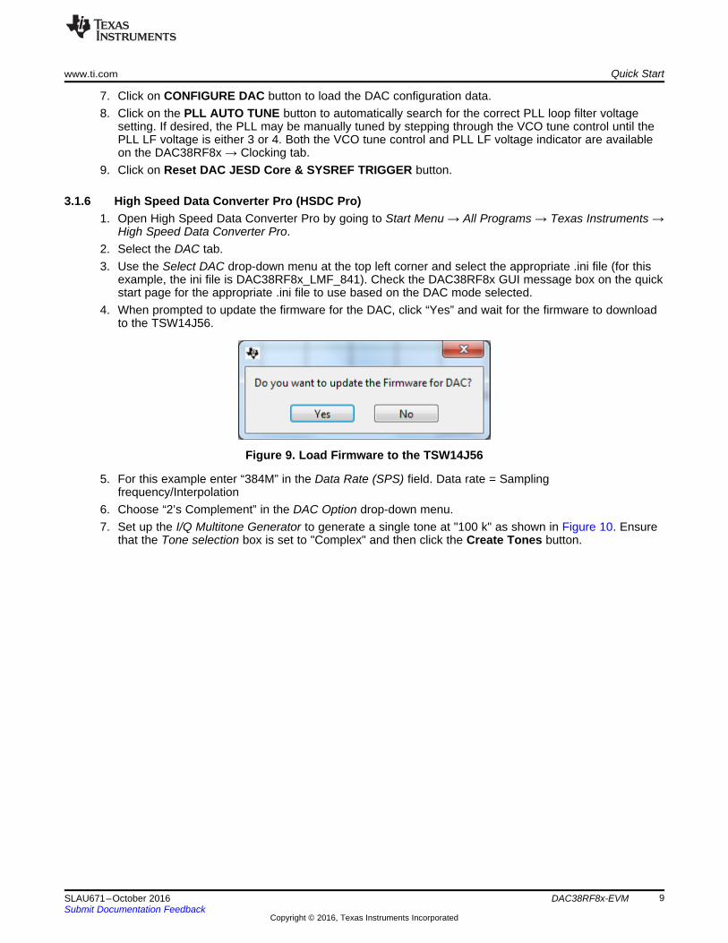
4. When prompted to update the firmware for the DAC, click “Yes” and wait for the firmware to downloadto the TSW14J56.
Figure 9. Load Firmware to the TSW14J56
5. For this example enter “384M” in the Data Rate (SPS) field. Data rate = Samplingfrequency/Interpolation
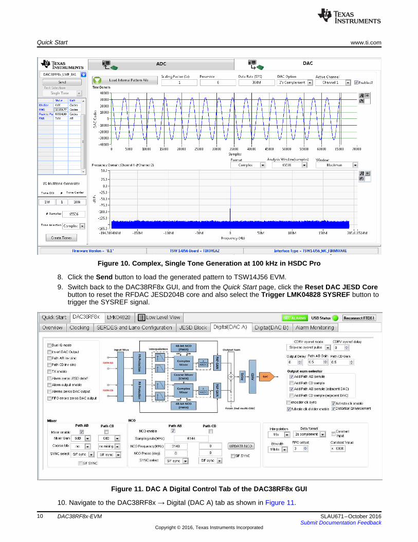
6. Choose “2’s Complement” in the DAC Option drop-down menu.7. Set up the I/Q Multitone Generator to generate a single tone at "100 k" as shown in Figure 10. Ensure
that the Tone selection box is set to "Complex" and then click the Create Tones button.
Quick Start www.ti.com
10 SLAU671–October 2016Submit Documentation Feedback
Copyright © 2016, Texas Instruments Incorporated
DAC38RF8x-EVM
Figure 10. Complex, Single Tone Generation at 100 kHz in HSDC Pro
8. Click the Send button to load the generated pattern to TSW14J56 EVM.9. Switch back to the DAC38RF8x GUI, and from the Quick Start page, click the Reset DAC JESD Core
button to reset the RFDAC JESD204B core and also select the Trigger LMK04828 SYSREF button totrigger the SYSREF signal.
Figure 11. DAC A Digital Control Tab of the DAC38RF8x GUI
10. Navigate to the DAC38RF8x → Digital (DAC A) tab as shown in Figure 11.
www.ti.com Quick Start
11SLAU671–October 2016Submit Documentation Feedback
Copyright © 2016, Texas Instruments Incorporated
DAC38RF8x-EVM
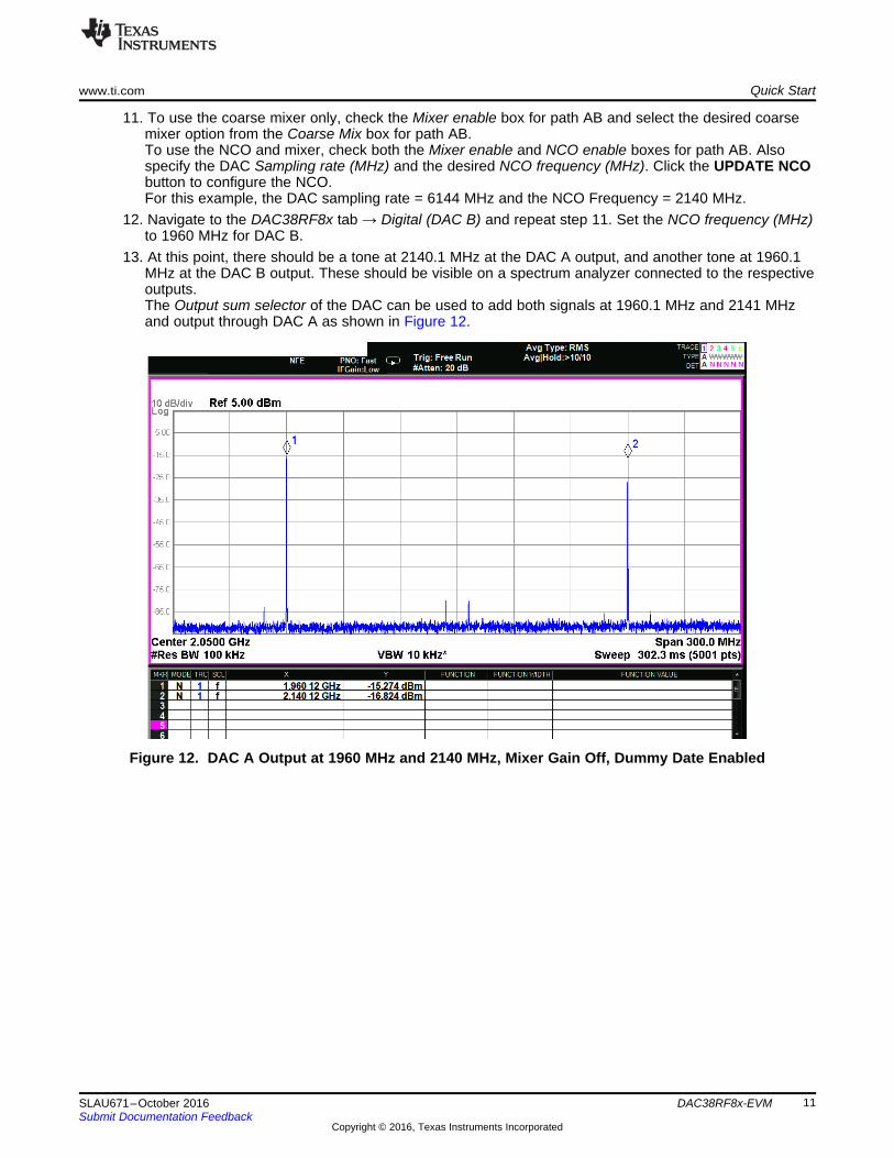
11. To use the coarse mixer only, check the Mixer enable box for path AB and select the desired coarsemixer option from the Coarse Mix box for path AB.To use the NCO and mixer, check both the Mixer enable and NCO enable boxes for path AB. Alsospecify the DAC Sampling rate (MHz) and the desired NCO frequency (MHz). Click the UPDATE NCObutton to configure the NCO.For this example, the DAC sampling rate = 6144 MHz and the NCO Frequency = 2140 MHz.
12. Navigate to the DAC38RF8x tab → Digital (DAC B) and repeat step 11. Set the NCO frequency (MHz)to 1960 MHz for DAC B.
13. At this point, there should be a tone at 2140.1 MHz at the DAC A output, and another tone at 1960.1MHz at the DAC B output. These should be visible on a spectrum analyzer connected to the respectiveoutputs.The Output sum selector of the DAC can be used to add both signals at 1960.1 MHz and 2141 MHzand output through DAC A as shown in Figure 12.
Figure 12. DAC A Output at 1960 MHz and 2140 MHz, Mixer Gain Off, Dummy Date Enabled
Quick Start www.ti.com
12 SLAU671–October 2016Submit Documentation Feedback
Copyright © 2016, Texas Instruments Incorporated
DAC38RF8x-EVM
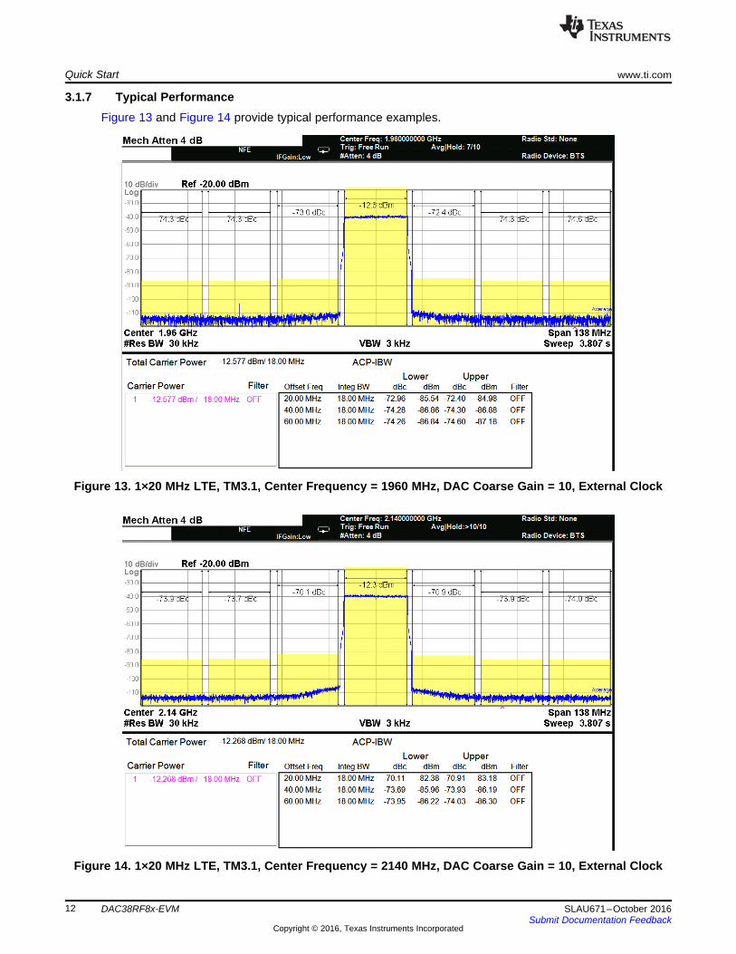
3.1.7 Typical PerformanceFigure 13 and Figure 14 provide typical performance examples.
Figure 13. 1×20 MHz LTE, TM3.1, Center Frequency = 1960 MHz, DAC Coarse Gain = 10, External Clock
Figure 14. 1×20 MHz LTE, TM3.1, Center Frequency = 2140 MHz, DAC Coarse Gain = 10, External Clock
Frequency (Hz)
Out
put P
ower
(dB
m)
0x10
0
2x10
8
4x10
8
6x10
8
8x10
8
1x10
9
1.2x
109
1.4x
109
1.6x
109
1.8x
109
2x10
9
2.2x
109
2.4x
109
2.6x
109
2.8x
109
3x10
9
3.2x
109
3.4x
109
3.6x
109
3.8x
109
4x10
9
4.2x
109
4.4x
109
-20
-15
-10
-5
0
5
10
D001
DAC38RF83DAC38RF80
www.ti.com Known Issues
13SLAU671–October 2016Submit Documentation Feedback
Copyright © 2016, Texas Instruments Incorporated
DAC38RF8x-EVM
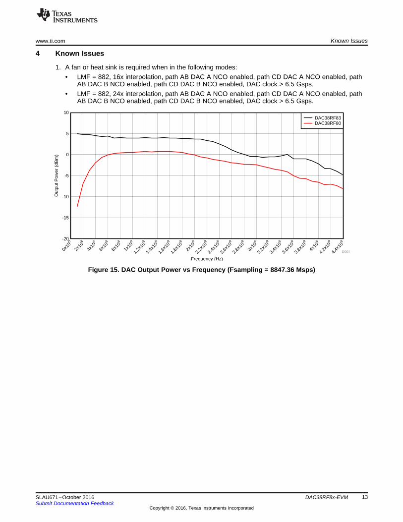
4 Known Issues
1. A fan or heat sink is required when in the following modes:• LMF = 882, 16x interpolation, path AB DAC A NCO enabled, path CD DAC A NCO enabled, path
AB DAC B NCO enabled, path CD DAC B NCO enabled, DAC clock > 6.5 Gsps.• LMF = 882, 24x interpolation, path AB DAC A NCO enabled, path CD DAC A NCO enabled, path
AB DAC B NCO enabled, path CD DAC B NCO enabled, DAC clock > 6.5 Gsps.
Figure 15. DAC Output Power vs Frequency (Fsampling = 8847.36 Msps)
Amplitude Unbalance Phase Unbalance
Frequency (MHz) Frequency (MHz)
Frequency (MHz) Frequency (MHz)
Inse
rtio
n Lo
ss (
db)
Average Insertion Loss Input Return Loss
Am
plitu
de U
nbal
ance
(db
)
Pha
se U
nbal
ance
(de
g)In
put R
etur
n Lo
ss (
dB)
14 SLAU671–October 2016Submit Documentation Feedback
Copyright © 2016, Texas Instruments Incorporated
Appendix ASLAU671–October 2016
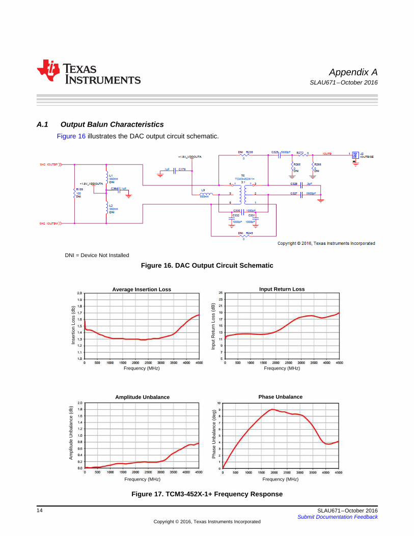
A.1 Output Balun CharacteristicsFigure 16 illustrates the DAC output circuit schematic.
DNI = Device Not Installed
Figure 16. DAC Output Circuit Schematic
Figure 17. TCM3-452X-1+ Frequency Response
Amplitude Unbalance Phase Unbalance
Frequency (MHz) Frequency (MHz)
Frequency (MHz) Frequency (MHz)
Inse
rtio
n Lo
ss (
db)
Average Insertion Loss Input Return Loss
Am
plitu
de U
nbal
ance
(db
)
Pha
se U
nbal
ance
(de
g)In
put R
etur
n Lo
ss (
dB)
15SLAU671–October 2016Submit Documentation Feedback
Copyright © 2016, Texas Instruments Incorporated
Appendix BSLAU671–October 2016
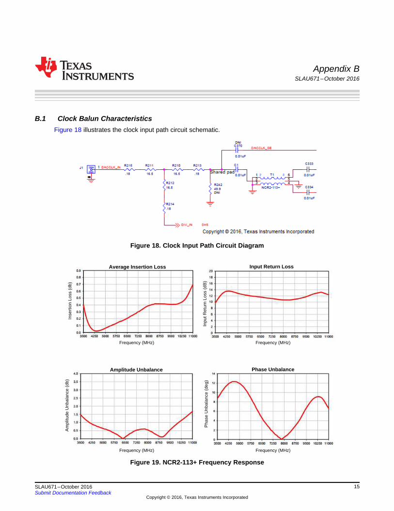
B.1 Clock Balun CharacteristicsFigure 18 illustrates the clock input path circuit schematic.
Figure 18. Clock Input Path Circuit Diagram
Figure 19. NCR2-113+ Frequency Response
STANDARD TERMS AND CONDITIONS FOR EVALUATION MODULES1. Delivery: TI delivers TI evaluation boards, kits, or modules, including demonstration software, components, and/or documentation
which may be provided together or separately (collectively, an “EVM” or “EVMs”) to the User (“User”) in accordance with the termsand conditions set forth herein. Acceptance of the EVM is expressly subject to the following terms and conditions.1.1 EVMs are intended solely for product or software developers for use in a research and development setting to facilitate feasibility
evaluation, experimentation, or scientific analysis of TI semiconductors products. EVMs have no direct function and are notfinished products. EVMs shall not be directly or indirectly assembled as a part or subassembly in any finished product. Forclarification, any software or software tools provided with the EVM (“Software”) shall not be subject to the terms and conditionsset forth herein but rather shall be subject to the applicable terms and conditions that accompany such Software
1.2 EVMs are not intended for consumer or household use. EVMs may not be sold, sublicensed, leased, rented, loaned, assigned,or otherwise distributed for commercial purposes by Users, in whole or in part, or used in any finished product or productionsystem.
2 Limited Warranty and Related Remedies/Disclaimers:2.1 These terms and conditions do not apply to Software. The warranty, if any, for Software is covered in the applicable Software
License Agreement.2.2 TI warrants that the TI EVM will conform to TI's published specifications for ninety (90) days after the date TI delivers such EVM
to User. Notwithstanding the foregoing, TI shall not be liable for any defects that are caused by neglect, misuse or mistreatmentby an entity other than TI, including improper installation or testing, or for any EVMs that have been altered or modified in anyway by an entity other than TI. Moreover, TI shall not be liable for any defects that result from User's design, specifications orinstructions for such EVMs. Testing and other quality control techniques are used to the extent TI deems necessary or asmandated by government requirements. TI does not test all parameters of each EVM.
2.3 If any EVM fails to conform to the warranty set forth above, TI's sole liability shall be at its option to repair or replace such EVM,or credit User's account for such EVM. TI's liability under this warranty shall be limited to EVMs that are returned during thewarranty period to the address designated by TI and that are determined by TI not to conform to such warranty. If TI elects torepair or replace such EVM, TI shall have a reasonable time to repair such EVM or provide replacements. Repaired EVMs shallbe warranted for the remainder of the original warranty period. Replaced EVMs shall be warranted for a new full ninety (90) daywarranty period.
3 Regulatory Notices:3.1 United States
3.1.1 Notice applicable to EVMs not FCC-Approved:This kit is designed to allow product developers to evaluate electronic components, circuitry, or software associated with the kitto determine whether to incorporate such items in a finished product and software developers to write software applications foruse with the end product. This kit is not a finished product and when assembled may not be resold or otherwise marketed unlessall required FCC equipment authorizations are first obtained. Operation is subject to the condition that this product not causeharmful interference to licensed radio stations and that this product accept harmful interference. Unless the assembled kit isdesigned to operate under part 15, part 18 or part 95 of this chapter, the operator of the kit must operate under the authority ofan FCC license holder or must secure an experimental authorization under part 5 of this chapter.3.1.2 For EVMs annotated as FCC – FEDERAL COMMUNICATIONS COMMISSION Part 15 Compliant:
CAUTIONThis device complies with part 15 of the FCC Rules. Operation is subject to the following two conditions: (1) This device may notcause harmful interference, and (2) this device must accept any interference received, including interference that may causeundesired operation.Changes or modifications not expressly approved by the party responsible for compliance could void the user's authority tooperate the equipment.
FCC Interference Statement for Class A EVM devicesNOTE: This equipment has been tested and found to comply with the limits for a Class A digital device, pursuant to part 15 ofthe FCC Rules. These limits are designed to provide reasonable protection against harmful interference when the equipment isoperated in a commercial environment. This equipment generates, uses, and can radiate radio frequency energy and, if notinstalled and used in accordance with the instruction manual, may cause harmful interference to radio communications.Operation of this equipment in a residential area is likely to cause harmful interference in which case the user will be required tocorrect the interference at his own expense.
SPACER
SPACER
SPACER
SPACER
SPACER
SPACER
SPACER
SPACER
FCC Interference Statement for Class B EVM devicesNOTE: This equipment has been tested and found to comply with the limits for a Class B digital device, pursuant to part 15 ofthe FCC Rules. These limits are designed to provide reasonable protection against harmful interference in a residentialinstallation. This equipment generates, uses and can radiate radio frequency energy and, if not installed and used in accordancewith the instructions, may cause harmful interference to radio communications. However, there is no guarantee that interferencewill not occur in a particular installation. If this equipment does cause harmful interference to radio or television reception, whichcan be determined by turning the equipment off and on, the user is encouraged to try to correct the interference by one or moreof the following measures:
• Reorient or relocate the receiving antenna.• Increase the separation between the equipment and receiver.• Connect the equipment into an outlet on a circuit different from that to which the receiver is connected.• Consult the dealer or an experienced radio/TV technician for help.
3.2 Canada3.2.1 For EVMs issued with an Industry Canada Certificate of Conformance to RSS-210
Concerning EVMs Including Radio Transmitters:This device complies with Industry Canada license-exempt RSS standard(s). Operation is subject to the following two conditions:(1) this device may not cause interference, and (2) this device must accept any interference, including interference that maycause undesired operation of the device.
Concernant les EVMs avec appareils radio:Le présent appareil est conforme aux CNR d'Industrie Canada applicables aux appareils radio exempts de licence. L'exploitationest autorisée aux deux conditions suivantes: (1) l'appareil ne doit pas produire de brouillage, et (2) l'utilisateur de l'appareil doitaccepter tout brouillage radioélectrique subi, même si le brouillage est susceptible d'en compromettre le fonctionnement.
Concerning EVMs Including Detachable Antennas:Under Industry Canada regulations, this radio transmitter may only operate using an antenna of a type and maximum (or lesser)gain approved for the transmitter by Industry Canada. To reduce potential radio interference to other users, the antenna typeand its gain should be so chosen that the equivalent isotropically radiated power (e.i.r.p.) is not more than that necessary forsuccessful communication. This radio transmitter has been approved by Industry Canada to operate with the antenna typeslisted in the user guide with the maximum permissible gain and required antenna impedance for each antenna type indicated.Antenna types not included in this list, having a gain greater than the maximum gain indicated for that type, are strictly prohibitedfor use with this device.
Concernant les EVMs avec antennes détachablesConformément à la réglementation d'Industrie Canada, le présent émetteur radio peut fonctionner avec une antenne d'un type etd'un gain maximal (ou inférieur) approuvé pour l'émetteur par Industrie Canada. Dans le but de réduire les risques de brouillageradioélectrique à l'intention des autres utilisateurs, il faut choisir le type d'antenne et son gain de sorte que la puissance isotroperayonnée équivalente (p.i.r.e.) ne dépasse pas l'intensité nécessaire à l'établissement d'une communication satisfaisante. Leprésent émetteur radio a été approuvé par Industrie Canada pour fonctionner avec les types d'antenne énumérés dans lemanuel d’usage et ayant un gain admissible maximal et l'impédance requise pour chaque type d'antenne. Les types d'antennenon inclus dans cette liste, ou dont le gain est supérieur au gain maximal indiqué, sont strictement interdits pour l'exploitation del'émetteur
3.3 Japan3.3.1 Notice for EVMs delivered in Japan: Please see http://www.tij.co.jp/lsds/ti_ja/general/eStore/notice_01.page 日本国内に
輸入される評価用キット、ボードについては、次のところをご覧ください。http://www.tij.co.jp/lsds/ti_ja/general/eStore/notice_01.page
3.3.2 Notice for Users of EVMs Considered “Radio Frequency Products” in Japan: EVMs entering Japan may not be certifiedby TI as conforming to Technical Regulations of Radio Law of Japan.
If User uses EVMs in Japan, not certified to Technical Regulations of Radio Law of Japan, User is required by Radio Law ofJapan to follow the instructions below with respect to EVMs:1. Use EVMs in a shielded room or any other test facility as defined in the notification #173 issued by Ministry of Internal
Affairs and Communications on March 28, 2006, based on Sub-section 1.1 of Article 6 of the Ministry’s Rule forEnforcement of Radio Law of Japan,
2. Use EVMs only after User obtains the license of Test Radio Station as provided in Radio Law of Japan with respect toEVMs, or
3. Use of EVMs only after User obtains the Technical Regulations Conformity Certification as provided in Radio Law of Japanwith respect to EVMs. Also, do not transfer EVMs, unless User gives the same notice above to the transferee. Please notethat if User does not follow the instructions above, User will be subject to penalties of Radio Law of Japan.
SPACER
SPACER
SPACER
SPACER
SPACER
【無線電波を送信する製品の開発キットをお使いになる際の注意事項】 開発キットの中には技術基準適合証明を受けていないものがあります。 技術適合証明を受けていないもののご使用に際しては、電波法遵守のため、以下のいずれかの措置を取っていただく必要がありますのでご注意ください。1. 電波法施行規則第6条第1項第1号に基づく平成18年3月28日総務省告示第173号で定められた電波暗室等の試験設備でご使用
いただく。2. 実験局の免許を取得後ご使用いただく。3. 技術基準適合証明を取得後ご使用いただく。
なお、本製品は、上記の「ご使用にあたっての注意」を譲渡先、移転先に通知しない限り、譲渡、移転できないものとします。上記を遵守頂けない場合は、電波法の罰則が適用される可能性があることをご留意ください。 日本テキサス・イ
ンスツルメンツ株式会社東京都新宿区西新宿6丁目24番1号西新宿三井ビル
3.3.3 Notice for EVMs for Power Line Communication: Please see http://www.tij.co.jp/lsds/ti_ja/general/eStore/notice_02.page電力線搬送波通信についての開発キットをお使いになる際の注意事項については、次のところをご覧ください。http://www.tij.co.jp/lsds/ti_ja/general/eStore/notice_02.page
SPACER4 EVM Use Restrictions and Warnings:
4.1 EVMS ARE NOT FOR USE IN FUNCTIONAL SAFETY AND/OR SAFETY CRITICAL EVALUATIONS, INCLUDING BUT NOTLIMITED TO EVALUATIONS OF LIFE SUPPORT APPLICATIONS.
4.2 User must read and apply the user guide and other available documentation provided by TI regarding the EVM prior to handlingor using the EVM, including without limitation any warning or restriction notices. The notices contain important safety informationrelated to, for example, temperatures and voltages.
4.3 Safety-Related Warnings and Restrictions:4.3.1 User shall operate the EVM within TI’s recommended specifications and environmental considerations stated in the user
guide, other available documentation provided by TI, and any other applicable requirements and employ reasonable andcustomary safeguards. Exceeding the specified performance ratings and specifications (including but not limited to inputand output voltage, current, power, and environmental ranges) for the EVM may cause personal injury or death, orproperty damage. If there are questions concerning performance ratings and specifications, User should contact a TIfield representative prior to connecting interface electronics including input power and intended loads. Any loads appliedoutside of the specified output range may also result in unintended and/or inaccurate operation and/or possiblepermanent damage to the EVM and/or interface electronics. Please consult the EVM user guide prior to connecting anyload to the EVM output. If there is uncertainty as to the load specification, please contact a TI field representative.During normal operation, even with the inputs and outputs kept within the specified allowable ranges, some circuitcomponents may have elevated case temperatures. These components include but are not limited to linear regulators,switching transistors, pass transistors, current sense resistors, and heat sinks, which can be identified using theinformation in the associated documentation. When working with the EVM, please be aware that the EVM may becomevery warm.
4.3.2 EVMs are intended solely for use by technically qualified, professional electronics experts who are familiar with thedangers and application risks associated with handling electrical mechanical components, systems, and subsystems.User assumes all responsibility and liability for proper and safe handling and use of the EVM by User or its employees,affiliates, contractors or designees. User assumes all responsibility and liability to ensure that any interfaces (electronicand/or mechanical) between the EVM and any human body are designed with suitable isolation and means to safelylimit accessible leakage currents to minimize the risk of electrical shock hazard. User assumes all responsibility andliability for any improper or unsafe handling or use of the EVM by User or its employees, affiliates, contractors ordesignees.
4.4 User assumes all responsibility and liability to determine whether the EVM is subject to any applicable international, federal,state, or local laws and regulations related to User’s handling and use of the EVM and, if applicable, User assumes allresponsibility and liability for compliance in all respects with such laws and regulations. User assumes all responsibility andliability for proper disposal and recycling of the EVM consistent with all applicable international, federal, state, and localrequirements.
5. Accuracy of Information: To the extent TI provides information on the availability and function of EVMs, TI attempts to be as accurateas possible. However, TI does not warrant the accuracy of EVM descriptions, EVM availability or other information on its websites asaccurate, complete, reliable, current, or error-free.
SPACER
SPACER
SPACER
SPACER
SPACER
SPACER
SPACER6. Disclaimers:
6.1 EXCEPT AS SET FORTH ABOVE, EVMS AND ANY WRITTEN DESIGN MATERIALS PROVIDED WITH THE EVM (AND THEDESIGN OF THE EVM ITSELF) ARE PROVIDED "AS IS" AND "WITH ALL FAULTS." TI DISCLAIMS ALL OTHERWARRANTIES, EXPRESS OR IMPLIED, REGARDING SUCH ITEMS, INCLUDING BUT NOT LIMITED TO ANY IMPLIEDWARRANTIES OF MERCHANTABILITY OR FITNESS FOR A PARTICULAR PURPOSE OR NON-INFRINGEMENT OF ANYTHIRD PARTY PATENTS, COPYRIGHTS, TRADE SECRETS OR OTHER INTELLECTUAL PROPERTY RIGHTS.
6.2 EXCEPT FOR THE LIMITED RIGHT TO USE THE EVM SET FORTH HEREIN, NOTHING IN THESE TERMS ANDCONDITIONS SHALL BE CONSTRUED AS GRANTING OR CONFERRING ANY RIGHTS BY LICENSE, PATENT, OR ANYOTHER INDUSTRIAL OR INTELLECTUAL PROPERTY RIGHT OF TI, ITS SUPPLIERS/LICENSORS OR ANY OTHER THIRDPARTY, TO USE THE EVM IN ANY FINISHED END-USER OR READY-TO-USE FINAL PRODUCT, OR FOR ANYINVENTION, DISCOVERY OR IMPROVEMENT MADE, CONCEIVED OR ACQUIRED PRIOR TO OR AFTER DELIVERY OFTHE EVM.
7. USER'S INDEMNITY OBLIGATIONS AND REPRESENTATIONS. USER WILL DEFEND, INDEMNIFY AND HOLD TI, ITSLICENSORS AND THEIR REPRESENTATIVES HARMLESS FROM AND AGAINST ANY AND ALL CLAIMS, DAMAGES, LOSSES,EXPENSES, COSTS AND LIABILITIES (COLLECTIVELY, "CLAIMS") ARISING OUT OF OR IN CONNECTION WITH ANYHANDLING OR USE OF THE EVM THAT IS NOT IN ACCORDANCE WITH THESE TERMS AND CONDITIONS. THIS OBLIGATIONSHALL APPLY WHETHER CLAIMS ARISE UNDER STATUTE, REGULATION, OR THE LAW OF TORT, CONTRACT OR ANYOTHER LEGAL THEORY, AND EVEN IF THE EVM FAILS TO PERFORM AS DESCRIBED OR EXPECTED.
8. Limitations on Damages and Liability:8.1 General Limitations. IN NO EVENT SHALL TI BE LIABLE FOR ANY SPECIAL, COLLATERAL, INDIRECT, PUNITIVE,
INCIDENTAL, CONSEQUENTIAL, OR EXEMPLARY DAMAGES IN CONNECTION WITH OR ARISING OUT OF THESETERMS ANDCONDITIONS OR THE USE OF THE EVMS PROVIDED HEREUNDER, REGARDLESS OF WHETHER TI HASBEEN ADVISED OF THE POSSIBILITY OF SUCH DAMAGES. EXCLUDED DAMAGES INCLUDE, BUT ARE NOT LIMITEDTO, COST OF REMOVAL OR REINSTALLATION, ANCILLARY COSTS TO THE PROCUREMENT OF SUBSTITUTE GOODSOR SERVICES, RETESTING, OUTSIDE COMPUTER TIME, LABOR COSTS, LOSS OF GOODWILL, LOSS OF PROFITS,LOSS OF SAVINGS, LOSS OF USE, LOSS OF DATA, OR BUSINESS INTERRUPTION. NO CLAIM, SUIT OR ACTION SHALLBE BROUGHT AGAINST TI MORE THAN ONE YEAR AFTER THE RELATED CAUSE OF ACTION HAS OCCURRED.
8.2 Specific Limitations. IN NO EVENT SHALL TI'S AGGREGATE LIABILITY FROM ANY WARRANTY OR OTHER OBLIGATIONARISING OUT OF OR IN CONNECTION WITH THESE TERMS AND CONDITIONS, OR ANY USE OF ANY TI EVMPROVIDED HEREUNDER, EXCEED THE TOTAL AMOUNT PAID TO TI FOR THE PARTICULAR UNITS SOLD UNDERTHESE TERMS AND CONDITIONS WITH RESPECT TO WHICH LOSSES OR DAMAGES ARE CLAIMED. THE EXISTENCEOF MORE THAN ONE CLAIM AGAINST THE PARTICULAR UNITS SOLD TO USER UNDER THESE TERMS ANDCONDITIONS SHALL NOT ENLARGE OR EXTEND THIS LIMIT.
9. Return Policy. Except as otherwise provided, TI does not offer any refunds, returns, or exchanges. Furthermore, no return of EVM(s)will be accepted if the package has been opened and no return of the EVM(s) will be accepted if they are damaged or otherwise not ina resalable condition. If User feels it has been incorrectly charged for the EVM(s) it ordered or that delivery violates the applicableorder, User should contact TI. All refunds will be made in full within thirty (30) working days from the return of the components(s),excluding any postage or packaging costs.
10. Governing Law: These terms and conditions shall be governed by and interpreted in accordance with the laws of the State of Texas,without reference to conflict-of-laws principles. User agrees that non-exclusive jurisdiction for any dispute arising out of or relating tothese terms and conditions lies within courts located in the State of Texas and consents to venue in Dallas County, Texas.Notwithstanding the foregoing, any judgment may be enforced in any United States or foreign court, and TI may seek injunctive reliefin any United States or foreign court.
Mailing Address: Texas Instruments, Post Office Box 655303, Dallas, Texas 75265Copyright © 2016, Texas Instruments Incorporated
spacer
IMPORTANT NOTICE
Texas Instruments Incorporated and its subsidiaries (TI) reserve the right to make corrections, enhancements, improvements and otherchanges to its semiconductor products and services per JESD46, latest issue, and to discontinue any product or service per JESD48, latestissue. Buyers should obtain the latest relevant information before placing orders and should verify that such information is current andcomplete. All semiconductor products (also referred to herein as “components”) are sold subject to TI’s terms and conditions of salesupplied at the time of order acknowledgment.TI warrants performance of its components to the specifications applicable at the time of sale, in accordance with the warranty in TI’s termsand conditions of sale of semiconductor products. Testing and other quality control techniques are used to the extent TI deems necessaryto support this warranty. Except where mandated by applicable law, testing of all parameters of each component is not necessarilyperformed.TI assumes no liability for applications assistance or the design of Buyers’ products. Buyers are responsible for their products andapplications using TI components. To minimize the risks associated with Buyers’ products and applications, Buyers should provideadequate design and operating safeguards.TI does not warrant or represent that any license, either express or implied, is granted under any patent right, copyright, mask work right, orother intellectual property right relating to any combination, machine, or process in which TI components or services are used. Informationpublished by TI regarding third-party products or services does not constitute a license to use such products or services or a warranty orendorsement thereof. Use of such information may require a license from a third party under the patents or other intellectual property of thethird party, or a license from TI under the patents or other intellectual property of TI.Reproduction of significant portions of TI information in TI data books or data sheets is permissible only if reproduction is without alterationand is accompanied by all associated warranties, conditions, limitations, and notices. TI is not responsible or liable for such altereddocumentation. Information of third parties may be subject to additional restrictions.Resale of TI components or services with statements different from or beyond the parameters stated by TI for that component or servicevoids all express and any implied warranties for the associated TI component or service and is an unfair and deceptive business practice.TI is not responsible or liable for any such statements.Buyer acknowledges and agrees that it is solely responsible for compliance with all legal, regulatory and safety-related requirementsconcerning its products, and any use of TI components in its applications, notwithstanding any applications-related information or supportthat may be provided by TI. Buyer represents and agrees that it has all the necessary expertise to create and implement safeguards whichanticipate dangerous consequences of failures, monitor failures and their consequences, lessen the likelihood of failures that might causeharm and take appropriate remedial actions. Buyer will fully indemnify TI and its representatives against any damages arising out of the useof any TI components in safety-critical applications.In some cases, TI components may be promoted specifically to facilitate safety-related applications. With such components, TI’s goal is tohelp enable customers to design and create their own end-product solutions that meet applicable functional safety standards andrequirements. Nonetheless, such components are subject to these terms.No TI components are authorized for use in FDA Class III (or similar life-critical medical equipment) unless authorized officers of the partieshave executed a special agreement specifically governing such use.Only those TI components which TI has specifically designated as military grade or “enhanced plastic” are designed and intended for use inmilitary/aerospace applications or environments. Buyer acknowledges and agrees that any military or aerospace use of TI componentswhich have not been so designated is solely at the Buyer's risk, and that Buyer is solely responsible for compliance with all legal andregulatory requirements in connection with such use.TI has specifically designated certain components as meeting ISO/TS16949 requirements, mainly for automotive use. In any case of use ofnon-designated products, TI will not be responsible for any failure to meet ISO/TS16949.
Products ApplicationsAudio www.ti.com/audio Automotive and Transportation www.ti.com/automotiveAmplifiers amplifier.ti.com Communications and Telecom www.ti.com/communicationsData Converters dataconverter.ti.com Computers and Peripherals www.ti.com/computersDLP® Products www.dlp.com Consumer Electronics www.ti.com/consumer-appsDSP dsp.ti.com Energy and Lighting www.ti.com/energyClocks and Timers www.ti.com/clocks Industrial www.ti.com/industrialInterface interface.ti.com Medical www.ti.com/medicalLogic logic.ti.com Security www.ti.com/securityPower Mgmt power.ti.com Space, Avionics and Defense www.ti.com/space-avionics-defenseMicrocontrollers microcontroller.ti.com Video and Imaging www.ti.com/videoRFID www.ti-rfid.comOMAP Applications Processors www.ti.com/omap TI E2E Community e2e.ti.comWireless Connectivity www.ti.com/wirelessconnectivity
Mailing Address: Texas Instruments, Post Office Box 655303, Dallas, Texas 75265Copyright © 2016, Texas Instruments Incorporated
Mouser Electronics
Authorized Distributor
Click to View Pricing, Inventory, Delivery & Lifecycle Information: Texas Instruments:
DAC38RF82EVM


